41
1 COMP541 COMP541 Memories - I Memories - I Montek Singh Montek Singh Feb 29, 2012 Feb 29, 2012
| Date post: | 30-Dec-2015 |
| Category: |
Documents |
| Upload: | clement-garrison |
| View: | 214 times |
| Download: | 0 times |

1
COMP541COMP541
Memories - IMemories - I
Montek SinghMontek Singh
Feb 29, 2012Feb 29, 2012

TopicsTopics This week’s assignmentsThis week’s assignments
Homework #1 & Lab #6Homework #1 & Lab #6Everyone finished with them?Everyone finished with them?
First TestFirst Test Late MarchLate March
will announce date after Spring Breakwill announce date after Spring Break
Overview of Memory TypesOverview of Memory Types Read-Only Memory (ROM): PROMs, FLASH, etc.Read-Only Memory (ROM): PROMs, FLASH, etc. Random-Access Memory (RAM)Random-Access Memory (RAM)
Static todayStatic todayDynamic nextDynamic next
2

Types of MemoryTypes of Memory Many dimensionsMany dimensions
Read Only vs. Read/Write (or write seldom)Read Only vs. Read/Write (or write seldom) Volatile vs. Non-VolatileVolatile vs. Non-Volatile Requires refresh or notRequires refresh or not
Look at ROM first to examine interfaceLook at ROM first to examine interface
3

Non-Volatile Memory Non-Volatile Memory TechnologiesTechnologies Mask (old) Mask (old) ROM ROM
read-only memoryread-only memory
Fuses (old) Fuses (old) PROM PROM programmable read-only memoryprogrammable read-only memory
Erasable Erasable EPROM EPROM erasable programmable read-only memoryerasable programmable read-only memory
Electrically erasable Electrically erasable EEPROM EEPROM electrically-erasable programmable read-only memoryelectrically-erasable programmable read-only memory today called FLASH!today called FLASH!
used everywhere!used everywhere!
4

Details of ROMDetails of ROM Memory that is permanentMemory that is permanent
k address linesk address lines 22kk items items n bitsn bits
5

Notional View of InternalsNotional View of Internals
6
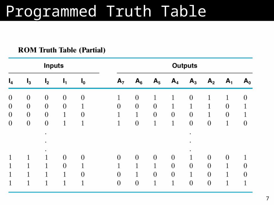
Programmed Truth TableProgrammed Truth Table
7

Resulting ProgrammingResulting Programming
8
In truth, theyIn truth, they’’re laid out in 2D (row, col)re laid out in 2D (row, col)

Mask ROMsMask ROMs Oldest technologyOldest technology Originally Originally ““maskmask”” used as last step in used as last step in
manufacturingmanufacturing Specify metal layer (connections)Specify metal layer (connections) Used for volume applicationsUsed for volume applications Long turnaroundLong turnaround Used for applications such as embedded systems and, Used for applications such as embedded systems and,
in the old days, boot ROMin the old days, boot ROM
but cheap to mass produce!but cheap to mass produce!
9

Programmable ROM (PROM)Programmable ROM (PROM) Early ones had fusible linksEarly ones had fusible links
High voltage would blow out linksHigh voltage would blow out links Fast to programFast to program Single useSingle use
10

UV EPROMUV EPROM ErasableErasable PROM PROM
Common technologies used UV light to erase Common technologies used UV light to erase complete devicecomplete device
Took about 10 minutesTook about 10 minutes Holds state as charge in very well insulated areas of Holds state as charge in very well insulated areas of
the chipthe chip Nonvolatile for several (10?) yearsNonvolatile for several (10?) years
11

EEPROMEEPROM Electrically Erasable PROMElectrically Erasable PROM
Similar technology to UV EPROMSimilar technology to UV EPROM Erased in blocks by higher voltageErased in blocks by higher voltage Programming is slower than readingProgramming is slower than reading
Today called “flash memory”Today called “flash memory” Digital cameras, MP3 players, BIOSDigital cameras, MP3 players, BIOS Limited lifeLimited life Some support individual word write, some blockSome support individual word write, some block
Our boards have it:Our boards have it: A flash memory chip on our Nexys 3 boardsA flash memory chip on our Nexys 3 boards Has a “boot block” that is carefully protectedHas a “boot block” that is carefully protected We will learn to use it in upcoming labsWe will learn to use it in upcoming labs
12

How Flash WorksHow Flash Works Special transistor with floating gateSpecial transistor with floating gate This is part of device surrounded by insulationThis is part of device surrounded by insulation
So charge placed there can stay for yearsSo charge placed there can stay for years Aside: some newer devices store multiple bits of info Aside: some newer devices store multiple bits of info
in a cellin a cell
Interested in this? If so, we can cover in more Interested in this? If so, we can cover in more detail w/ transistorsdetail w/ transistors
13

Read/Write MemoriesRead/Write Memories Flash is obviously writeableFlash is obviously writeable
But not meant to be written rapidly (say at CPU rates)But not meant to be written rapidly (say at CPU rates) And often writing must be by entire blocks (disk And often writing must be by entire blocks (disk
replacement)replacement)
For frequent writing, use RAMFor frequent writing, use RAM
14

Random Access MemoriesRandom Access Memories So called because it takes same amount of So called because it takes same amount of
time to address any particular locationtime to address any particular location Not entirely true for modern DRAMs, but somewhat Not entirely true for modern DRAMs, but somewhat
true…true…
First look at asynchronous static RAMFirst look at asynchronous static RAM Ones on Xilinx chip is synchronousOnes on Xilinx chip is synchronous
Data available at clock edges, like registersData available at clock edges, like registers One on board can be bothOne on board can be both Will cover details of board memory in the labWill cover details of board memory in the lab
15

Simple View of RAMSimple View of RAM Typical parameters:Typical parameters:
some word size some word size nn some capacity 2some capacity 2kk
k bits of address linek bits of address line
Need a line to specify reading or writingNeed a line to specify reading or writing typically only one wire neededtypically only one wire needed
sometimes two separate onessometimes two separate ones
16

Example: 1K x 16 memoryExample: 1K x 16 memory RAM comes in variety of RAM comes in variety of
sizessizes from 1-bit widefrom 1-bit wide main issue is no. of pins main issue is no. of pins
available on chipavailable on chip
Memory size often Memory size often specified in bytesspecified in bytes This would be 2KB memoryThis would be 2KB memory 10 address lines (=1K 10 address lines (=1K
locations)locations) 16 data lines (=2 16 data lines (=2
bytes/location)bytes/location)
17

WritingWriting Sequence of stepsSequence of steps
Setup address linesSetup address lines Setup data linesSetup data lines Activate write line (e.g., maybe a positive edge)Activate write line (e.g., maybe a positive edge)
18

ReadingReading StepsSteps
Setup address linesSetup address lines Activate read lineActivate read line Data available soonData available soon
for for asynchronousasynchronous memory: after simply a specified memory: after simply a specified amount of timeamount of time
for for synchronoussynchronous memory: after a clock edge memory: after a clock edge
19

Chip SelectChip Select Enable:Enable:
Usually a line to Usually a line to enableenable the chip the chip Why?Why?
20

Timing: WritingTiming: Writing
21

Timing: ReadingTiming: Reading
22

Static vs. Dynamic RAMStatic vs. Dynamic RAM Different internal implementations: SRAM vs. Different internal implementations: SRAM vs.
DRAMDRAM DRAM:DRAM:
DRAM stores charge in capacitorDRAM stores charge in capacitorDisappears after short period of timeDisappears after short period of timeMust be refreshedMust be refreshedSmall sizeSmall sizeHigher storage density Higher storage density larger capacities larger capacities
SRAM:SRAM:SRAM easier to useSRAM easier to useUses transistors (think of it as latch)Uses transistors (think of it as latch)FasterFasterMore expensive per bitMore expensive per bitSmaller sizesSmaller sizes
23

Structure of SRAMStructure of SRAM Internally, each bit stored in a “latch”Internally, each bit stored in a “latch”
One memory One memory cell cell per bitper bitCell consists of one or more transistorsCell consists of one or more transistorsNot really a latch made of NANDs/NORs, but logically Not really a latch made of NANDs/NORs, but logically
equivalentequivalentBehaves like an SR latchBehaves like an SR latch
Control logicControl logicalso need extra logic around the latch to make it work like also need extra logic around the latch to make it work like
a memory cella memory cell
24

Structure of SRAMStructure of SRAM Several optimized circuits often usedSeveral optimized circuits often used
replace a full-fledged SR latch with something replace a full-fledged SR latch with something simpler, smaller, faster…simpler, smaller, faster…Not really a latch made of NANDs/NORs, but logically Not really a latch made of NANDs/NORs, but logically
equivalentequivalentBehaves like an SR latchBehaves like an SR latch
e.g., a simpler 6-transistor memory celle.g., a simpler 6-transistor memory cell
25
wordline
bitline bitline

Example: A Simple OrganizationExample: A Simple Organization Note:Note:
In reality, more complexIn reality, more complex Only one word-line is “on” at a timeOnly one word-line is “on” at a time
26
wordline311
10
2:4Decoder
Address
01
00
storedbit = 0
wordline2
wordline1
wordline0
storedbit = 1
storedbit = 0
storedbit = 1
storedbit = 0
storedbit = 0
storedbit = 1
storedbit = 1
storedbit = 0
storedbit = 0
storedbit = 1
storedbit = 1
bitline2 bitline1 bitline0
Data2 Data1 Data0
2
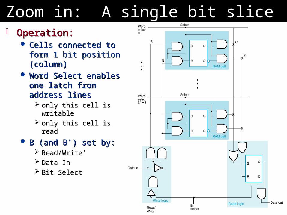
Zoom in: A single bit sliceZoom in: A single bit slice Operation:Operation:
Cells connected to Cells connected to form 1 bit position form 1 bit position (column)(column)
Word Select enables Word Select enables one latch from address one latch from address lineslines
only this cell is writableonly this cell is writable only this cell is readonly this cell is read
B (and BB (and B’’) set by:) set by: Read/Write’Read/Write’ Data InData In Bit SelectBit Select
27

Let’s look at a single bit cellLet’s look at a single bit cell
stored bit
wordline
bitline
Example:
stored bit = 0
wordline = 1
stored bit = 1
stored bit = 0
stored bit = 1
bitline =
(a) (b)
wordline = 1
wordline = 0
wordline = 0
bitline =
bitline =
bitline =0
1
Z
Z

29
Bit Slices and ModulesBit Slices and Modules Entire column of cellsEntire column of cells
called a bit slicecalled a bit slice basically a 1-bit wide basically a 1-bit wide
memory!memory!
ModuleModule module refers to a single module refers to a single
chip of memorychip of memory 1-bit wide memory chips are 1-bit wide memory chips are
quite common!quite common!

Inside an SRAM Bit CellInside an SRAM Bit Cell Actual implementation does not use a real SR Actual implementation does not use a real SR
latch!latch! a tinier approximation is useda tinier approximation is used logically behaves very much like an SR latchlogically behaves very much like an SR latch but much smaller and faster!but much smaller and faster!
stored bit
wordline
bitline
wordline
bitline bitline

31
16 X 1 RAM 16 X 1 RAM ““ChipChip””
Now shows Now shows address address decoderdecoder selects selects
appropriate appropriate locationlocation

Row/Column LayoutRow/Column Layout For larger RAMs:For larger RAMs:
decoder becomes pretty bigdecoder becomes pretty big also run into chip layout issuesalso run into chip layout issues
Typically:Typically: larger memories use larger memories use ““2D2D”” matrix layout matrix layout see next slidesee next slide
32

33
16 X 1 RAM as 4 X 4 Array16 X 1 RAM as 4 X 4 Array
Two decodersTwo decoders RowRow ColumnColumn
Address just Address just broken upbroken up
Not visible Not visible from outside from outside on SRAMson SRAMs

34
Not the same as 8 X 2 RAM!Not the same as 8 X 2 RAM! Minor change in Minor change in
logic and pinslogic and pins Spot the difference!Spot the difference!

Spot the difference!Spot the difference!
35

Realistic SizesRealistic Sizes Example: 256Kb memory organized 32K X 8Example: 256Kb memory organized 32K X 8
Single-column layout would need 15-bit decoder with Single-column layout would need 15-bit decoder with 32K outputs!32K outputs!
Better organization:Better organization: A 2D (i.e., square) layout with:A 2D (i.e., square) layout with:
9-bit row and 6-bit column decoders9-bit row and 6-bit column decoders
36

SRAM PerformanceSRAM Performance Latency and Throughput importantLatency and Throughput important
Current ones have cycle times in low nanoseconds Current ones have cycle times in low nanoseconds (say 2ns)(say 2ns)
Used as cache (typically on-chip or off-chip secondary Used as cache (typically on-chip or off-chip secondary cache)cache)
Sizes up to 8Mbit or so for fast chipsSizes up to 8Mbit or so for fast chips Expensive ones can go a bit biggerExpensive ones can go a bit bigger
Energy/powerEnergy/power SRAMs also better for low power vs. DRAMsSRAMs also better for low power vs. DRAMs
37

Wider MemoryWider Memory What if you donWhat if you don’’t have enough bit width?t have enough bit width?
use multiple chips and side-by-sideuse multiple chips and side-by-side
38
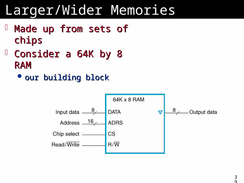
Larger/Wider MemoriesLarger/Wider Memories Made up from sets of Made up from sets of
chipschips Consider a 64K by 8 Consider a 64K by 8
RAMRAM our building blockour building block
39

LargerLarger Let’s build a larger Let’s build a larger
memorymemory 256K X 8256K X 8 Decoder for high-Decoder for high-
order 2 bitsorder 2 bitsSelects chipSelects chipLook at selection Look at selection
logiclogicAddress rangesAddress ranges
Tri-state outputsTri-state outputs
40

TodayToday Today we looked at:Today we looked at:
Quick look at non-volatile memoryQuick look at non-volatile memory Static RAMStatic RAM
Next class:Next class: Dynamic RAMDynamic RAM
Complex, largest, cheapComplex, largest, cheapMuch more design effort to useMuch more design effort to use
Talk about memories for labTalk about memories for lab
41


