KOREA UNIVERSITY Photonics Laboratory 3. Carrier action (a) Under normal operating conditions the three primary types of carrier action occurring inside semiconductors are drift, diffusion, and recombination-generation. (b) In this chapter we first describe each primary type of carrier action qualitatively and then quantitatively relate the action to the current flowing within the semiconductor. (1) Drift (1-1) Definition (a) Drift is charged-particle motion in response to an applied electric field: When an electric field () is applied across a semiconductor, the resulting force on the carriers tends to accelerate the +q charged holes in the direction of the electric field and the –q charged electrons in the direction opposite to the electric field. (b) Because of collisions with ionized impurity atoms and thermally agitated lattice atoms, however, the carrier acceleration is frequently interrupted (the carriers are said to be scattered). Averaging over all electrons or holes at any given time, we find that the resultant motion of each carrier type can be described in terms of a constant drift velocity v d . 1 3. Carrier action
Transcript
KOREA UNIVERSITY
Photonics Laboratory
3. Carrier action
(a) Under normal operating conditions the three primary types of carrier action occurring inside
semiconductors are drift, diffusion, and recombination-generation.
(b) In this chapter we first describe each primary type of carrier action qualitatively and then
quantitatively relate the action to the current flowing within the semiconductor.
(1) Drift
(1-1) Definition
(a) Drift is charged-particle motion in response to an applied electric field: When an electric field
(𝜀) is applied across a semiconductor, the resulting force on the carriers tends to accelerate the
+q charged holes in the direction of the electric field and the –q charged electrons in the
direction opposite to the electric field.
(b) Because of collisions with ionized impurity atoms and thermally agitated lattice atoms,
however, the carrier acceleration is frequently interrupted (the carriers are said to be
scattered). Averaging over all electrons or holes at any given time, we find that the resultant
motion of each carrier type can be described in terms of a constant drift velocity vd.
1
3. Carrier action
KOREA UNIVERSITY
Photonics Laboratory
(1-2) Drift current
).v-qnJ(drift ofdirection thecounter toin turn is particles charged negativelyby
ansportedcurrent tr the),-v( eldelectricfi applied the
tooppositedirection in thedrift electronsalthough that,Note *
(3.4b) nqJ
electrons
(3.4a) pqJ
holes) ( v
limit, field-low In the
(3.1)current drift hole :AqpvI
A, area sectional-cross ofbar tor semiconduc type-p thegConsiderin
dn/drift
nd
nn/drift
pp/drift
pd
dp/drift
For
for
2
(1-2) Drift current
KOREA UNIVERSITY
Photonics Laboratory
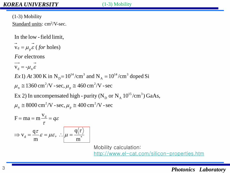
(1-3) Mobility
Standard units: cm2/V-sec.
*d
d
2
p
2
n
315
AD
2
p
2
n
314
A
314
D
nd
pd
m
q ,
m
qv
vmmaF
sec-/Vcm 400 sec,-/Vcm 0008
GaAs, )/cm10 Nor (Npurity -high teduncompensaIn 2)Ex