3.3-V/5-V HIGH-SPEED DIGITAL ISOLATORS• Signaling Rate 0 Mbps to 150 Mbps
23• Controlled Baseline – Low Propagation Delay– One Assembly Site – Low Pulse Skew (Pulse-Width Distortion)– One Test Site • Low-Power Sleep Mode– One Fabrication Site • High Electromagnetic Immunity
• Extended Temperature Performance of • Low Input Current Requirement–55°C to 125°C • Failsafe Output
• Enhanced Diminishing Manufacturing Sources • Drop-In Replacement for Most Opto and(DMS) Support Magnetic Isolators
– Modbus• 4000-V(peak) Isolation– Profibus– UL 1577, IEC 60747-5-2 (VDE 0884, Rev. 2)– DeviceNet™ Data BusesIEC 61010-1– Smart Distributed Systems (SDS™)– 50-kV/µs Transient Immunity Typical
• Computer Peripheral Interface(1) Component qualification in accordance with JEDEC andindustry standards to ensure reliable operation over an • Servo Control Interfaceextended temperature range. This includes, but is not limited
• Data Acquisitionto, Highly Accelerated Stress Test (HAST) or biased 85/85,temperature cycle, autoclave or unbiased HAST,electromigration, bond intermetallic life, and mold compoundlife. Such qualification testing should not be viewed asjustifying use of this component beyond specifiedperformance and environmental limits.
The ISO721, ISO721M, ISO722, and ISO722M are digital isolators with a logic input and output buffer separatedby a silicon oxide (SiO2) insulation barrier. This barrier provides galvanic isolation of up to 4000 V. Used inconjunction with isolated power supplies, these devices prevent noise currents on a data bus or other circuitsfrom entering the local ground, and interfering with or damaging sensitive circuitry.
A binary input signal is conditioned, translated to a balanced signal, then differentiated by the capacitive isolationbarrier. Across the isolation barrier, a differential comparator receives the logic transition information, then sets orresets a flip-flop and the output circuit accordingly. A periodic update pulse is sent across the barrier to ensurethe proper dc level of the output. If this dc-refresh pulse is not received for more than 4 µs, the input is assumedto be unpowered or not being actively driven, and the failsafe circuit drives the output to a logic high state.
1
Please be aware that an important notice concerning availability, standard warranty, and use in critical applications of TexasInstruments semiconductor products and disclaimers thereto appears at the end of this data sheet.
2SDS is a trademark of Honeywell.3DeviceNet is a trademark of Open Devicenet Vendors Association, Inc.
These devices have limited built-in ESD protection. The leads should be shorted together or the device placed in conductive foamduring storage or handling to prevent electrostatic damage to the MOS gates.
The symmetry of the dielectric and capacitor within the integrated circuitry provides for close capacitive matching,and allows fast transient voltage changes between the input and output grounds without corrupting the output.The small capacitance and resulting time constant provide for fast operation with signaling rates (2) from 0 Mbps(dc) to 100 Mbps for the ISO721/ISO722, and 0 Mbps to 150 Mbps with the ISO721M/ISO722M.
These devices require two supply voltages of 3.3 V, 5 V, or any combination. All inputs are 5-V tolerant whensupplied from a 3.3-V supply and all outputs are 4-mA CMOS.
The ISO721 has TTL input thresholds and a noise-filter at the input that prevents transient pulses of up to 2 ns induration from being passed to the output of the device.
The ISO721M has CMOS VCC/2 input thresholds, but do not have the noise filter and the additional propagationdelay. These features of the ISO721M also provide for reduced jitter operation.
The ISO721M is characterized for operation over the ambient temperature range of –55°C to 125°C.(2) The signaling rate of a line is the number of voltage transitions that are made per second expressed in the units bps (bits per second).
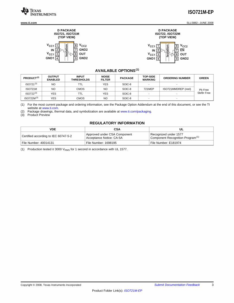
ISO721M NO CMOS NO SOIC-8 721MEP ISO721MMDREP (reel) Pb FreeSb/Br FreeISO722 (3) YES TTL YES SOIC-8 - -
ISO722M (3) YES CMOS NO SOIC-8 - -
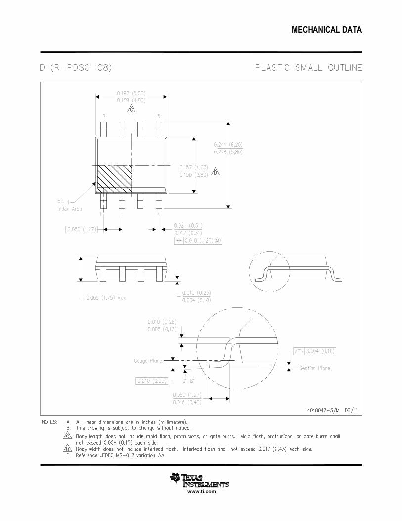
(1) For the most current package and ordering information, see the Package Option Addendum at the end of this document, or see the TIwebsite at www.ti.com.
(2) Package drawings, thermal data, and symbolization are available at www.ti.com/packaging.(3) Product Preview
REGULATORY INFORMATIONVDE CSA UL
Approved under CSA Component Recognized under 1577Certified according to IEC 60747-5-2 Acceptance Notice: CA-5A Component Recognition Program (1)
UNITVCC Supply voltage (2), VCC1, VCC2 –0.5 V to 6 VVI Voltage at IN, OUT, or EN terminal –0.5 V to 6 VIO Output Current ±15 mA
Human-Body Model JEDEC Standard 22, Test Method A114-C.01 ±2 kVElectrostaticESD All pinsdischarge Charged-Device Model JEDEC Standard 22, Test Method C101 ±1 kVTJ Maximum junction temperature 170°C
(1) Stresses beyond those listed under "absolute maximum ratings" may cause permanent damage to the device. These are stress ratingsonly and functional operation of the device at these or any other conditions beyond those indicated under "recommended operatingconditions" is not implied. Exposure to absolute-maximum-rated conditions for extended periods may affect device reliability.
(2) All voltage values except differential I/O bus voltages are with respect to network ground terminal and are peak voltage values. Vrmsvalues are not listed in this publication.
MIN TYP MAX UNIT4.5 5.5
VCC Supply voltage, VCC1, VCC2 V3 3.6
IOH High-level output current 4 mAIOL Low-level output current -4
ISO72x 10tui Input pulse width ns
ISO72xM 6.67VIH High-level input voltage (IN, EN) 2 VCCISO72x VVIL Low-level input voltage (IN, EN) 0 0.8VIH High-level input voltage (IN, EN) 0.7 VCC VCCIOS72xM VVIL Low-level input voltage (IN, EN) 0 0.3 VCC
TJ Junction temperature See the Thermal Characteristics table 150 °CExternal magnetic field intensity per IEC 61000-4-8 and IEC 61000-4-9H 1000 A/mcertification
over recommended operating conditions (unless otherwise noted)
PARAMETER TEST CONDITIONS SPECIFICATIONS UNITVIORM Maximum working insulation voltage 560 V
After Input/Output Safety Test Subgroup 2/3VPR = VIORM × 1.2, t = 10 s, 672 VPartial discharge < 5 pCMethod a, VPR = VIORM × 1.6,
VPR Input to output test voltage Type and sample test with t = 10 s, 896 VPartial discharge < 5 pCMethod b1, VPR = VIORM × 1.875,100 % Production test with t = 1 s, 1050 VPartial discharge < 5 pC
VIOTM Transient overvoltage t = 60 s 4000 VRS Insulation resistance VIO = 500 V at TS >109 Ω
over recommended operating conditions (unless otherwise noted)
PARAMETER TEST CONDITIONS MIN TYP MAX UNITQuiescent 0.5 1
ICC1 VCC1 supply current VI = VCC or 0 V, No load mA25 Mbps 2 4Quiescent VI = VCC or 0 V, No load 8 12
ICC2 VCC2 supply current mA25 Mbps VI = VCC or 0 V, No load 10 14
IOH = -4 mA, See Figure 1 VCC – 0.8 4.6VOH High-level output voltage V
IOH = –20 µA, See Figure 1 VCC – 0.1 5IOL = 4 mA, See Figure 1 0.2 0.4
VOL Low-level output voltage VIOL = 20 µA, See Figure 1 0 0.1
VI(HYS) Input voltage hysteresis 150 mVIIH High-level input current IN at 2 V 10
µAIIL Low-level input current IN at 0.8 V –10
High-impedance outputIOZ ISO722, ISO722M EN, IN at VCC 1 µAcurrentCI Input capacitance to ground IN at VCC, VI = 0.4 sin (4E6πt) 1 pFCMTI Common-mode transient immunity VI = VCC or 0 V, See Figure 5 25 50 kV/µs
over recommended operating conditions (unless otherwise noted)
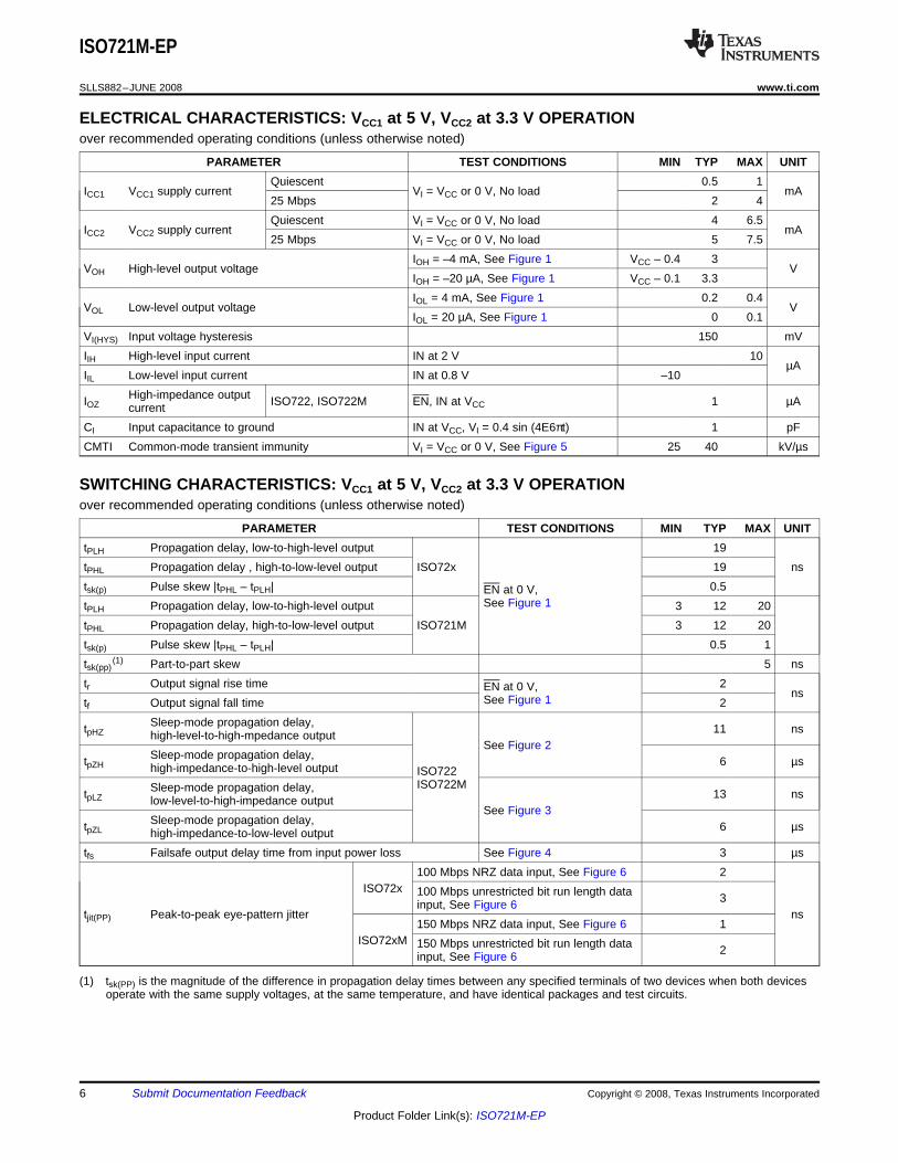
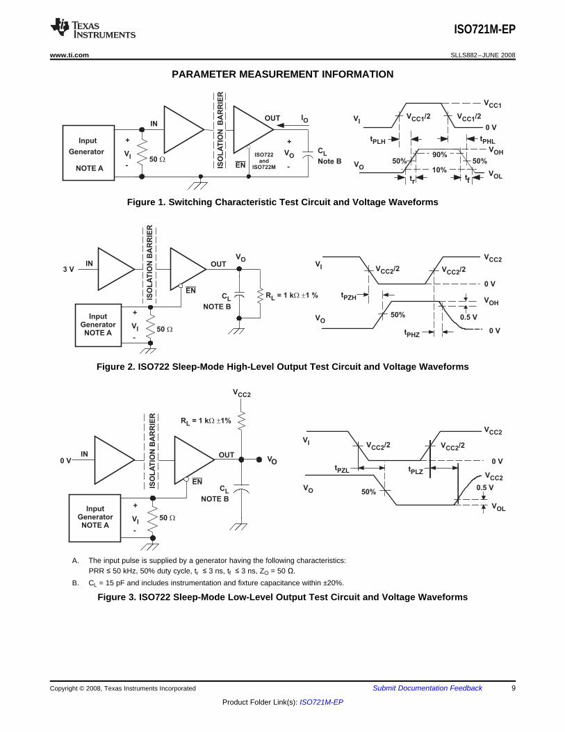
PARAMETER TEST CONDITIONS MIN TYP MAX UNITtPLH Propagation delay, low-to-high-level output 17tPHL Propagation delay , high-to-low-level output ISO72x 17 nstsk(p) Pulse skew |tPHL – tPLH| 0.5EN at 0 V,
See Figure 3Sleep-mode propagation delay,tpZL 5 µshigh-impedance-to-low-level output
tfs Failsafe output delay time from input power loss See Figure 4 3 µs100 Mbps NRZ data input, See Figure 6 2
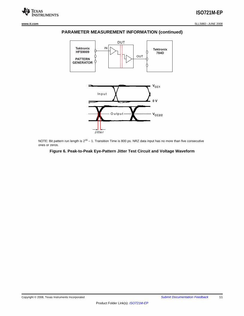
ISO72x 100 Mbps unrestricted bit run length data 3input, See Figure 6tjit(PP) Peak-to-peak eye-pattern jitter ns
150 Mbps NRZ data input, See Figure 6 1ISO72xM 150 Mbps unrestricted bit run length data 2input, See Figure 6
(1) tsk(PP) is the magnitude of the difference in propagation delay times between any specified terminals of two devices when both devicesoperate with the same supply voltages, at the same temperature, and have identical packages and test circuits.
over recommended operating conditions (unless otherwise noted)
PARAMETER TEST CONDITIONS MIN TYP MAX UNITQuiescent 0.5 1
ICC1 VCC1 supply current VI = VCC or 0 V, No load mA25 Mbps 2 4Quiescent VI = VCC or 0 V, No load 4 6.5
ICC2 VCC2 supply current mA25 Mbps VI = VCC or 0 V, No load 5 7.5
IOH = –4 mA, See Figure 1 VCC – 0.4 3VOH High-level output voltage V
IOH = –20 µA, See Figure 1 VCC – 0.1 3.3IOL = 4 mA, See Figure 1 0.2 0.4
VOL Low-level output voltage VIOL = 20 µA, See Figure 1 0 0.1
VI(HYS) Input voltage hysteresis 150 mVIIH High-level input current IN at 2 V 10
µAIIL Low-level input current IN at 0.8 V –10
High-impedance outputIOZ ISO722, ISO722M EN, IN at VCC 1 µAcurrentCI Input capacitance to ground IN at VCC, VI = 0.4 sin (4E6πt) 1 pFCMTI Common-mode transient immunity VI = VCC or 0 V, See Figure 5 25 40 kV/µs
over recommended operating conditions (unless otherwise noted)
PARAMETER TEST CONDITIONS MIN TYP MAX UNITtPLH Propagation delay, low-to-high-level output 19tPHL Propagation delay , high-to-low-level output ISO72x 19 nstsk(p) Pulse skew |tPHL – tPLH| 0.5EN at 0 V,
See Figure 3Sleep-mode propagation delay,tpZL 6 µshigh-impedance-to-low-level output
tfs Failsafe output delay time from input power loss See Figure 4 3 µs100 Mbps NRZ data input, See Figure 6 2
ISO72x 100 Mbps unrestricted bit run length data 3input, See Figure 6tjit(PP) Peak-to-peak eye-pattern jitter ns
150 Mbps NRZ data input, See Figure 6 1ISO72xM 150 Mbps unrestricted bit run length data 2input, See Figure 6
(1) tsk(PP) is the magnitude of the difference in propagation delay times between any specified terminals of two devices when both devicesoperate with the same supply voltages, at the same temperature, and have identical packages and test circuits.
over recommended operating conditions (unless otherwise noted)
PARAMETER TEST CONDITIONS MIN TYP MAX UNITQuiescent 0.3 0.5
ICC1 VCC1 supply current VI = VCC or 0 V, No load mA25 Mbps 1 2Quiescent VI = VCC or 0 V, No load 8 12
ICC2 VCC2 supply current mA25 Mbps VI = VCC or 0 V, No load 10 14
IOH = –4 mA, See Figure 1 VCC – 0.8 4.6VOH High-level output voltage V
IOH = –20 µA, See Figure 1 VCC – 0.1 5IOL = 4 mA, See Figure 1 0.2 0.4
VOL Low-level output voltage VIOL = 20 µA, See Figure 1 0 0.1
VI(HYS) Input voltage hysteresis 150 mVIIH High-level input current IN at 2 V 10
µAIIL Low-level input current IN at 0.8 V –10
High-impedance outputIOZ ISO722, ISO722M EN, IN at VCC 1 µAcurrentCI Input capacitance to ground IN at VCC, VI = 0.4 sin (4E6πt) 1 pFCMTI Common-mode transient immunity VI = VCC or 0 V, See Figure 5 25 40 kV/µs
over recommended operating conditions (unless otherwise noted)
PARAMETER TEST CONDITIONS MIN TYP MAX UNITtPLH Propagation delay, low-to-high-level output 17tPHL Propagation delay , high-to-low-level output ISO72x 17 nstsk(p) Pulse skew |tPHL – tPLH| 0.5EN at 0 V,
See Figure 3Sleep-mode propagation delay,tpZL 5 µshigh-impedance-to-low-level output
tfs Failsafe output delay time from input power loss See Figure 4 3 µs100 Mbps NRZ data input, See Figure 6 2
ISO72x 100 Mbps unrestricted bit run length data 3input, See Figure 6tjit(PP) Peak-to-peak eye-pattern jitter ns
150 Mbps NRZ data input, See Figure 6 1ISO72xM 150 Mbps unrestricted bit run length data 2input, See Figure 6
(1) tsk(PP) is the magnitude of the difference in propagation delay times between any specified terminals of two devices when both devicesoperate with the same supply voltages, at the same temperature, and have identical packages and test circuits.
over recommended operating conditions (unless otherwise noted)
PARAMETER TEST CONDITIONS MIN TYP MAX UNITQuiescent 0.3 0.5
ICC1 VCC1 supply current VI = VCC or 0 V, No load mA25 Mbps 1 2Quiescent VI = VCC or 0 V, No load 4 6.5
ICC2 VCC2 supply current mA25 Mbps VI = VCC or 0 V, No load 5 7.5
IOH = –4 mA, See Figure 1 VCC – 0.4 3VOH High-level output voltage V
IOH = –20 µA, See Figure 1 VCC – 0.1 3.3IOL = 4 mA, See Figure 1 0.2 0.4
VOL Low-level output voltage VIOL = 20 µA, See Figure 1 0 0.1
VI(HYS) Input voltage hysteresis 150 mVIIH High-level input current IN at 2 V 10
µAIIL Low-level input current IN at 0.8 V –10
High-impedance outputIOZ ISO722, ISO722M EN, IN at VCC 1 µAcurrentCI Input capacitance to ground IN at VCC, VI = 0.4 sin (4E6πt) 1 pFCMTI Common-mode transient immunity VI = VCC or 0 V, See Figure 5 25 40 kV/µs
over recommended operating conditions (unless otherwise noted)
PARAMETER TEST CONDITIONS MIN TYP MAX UNITtPLH Propagation delay, low-to-high-level output 20tPHL Propagation delay , high-to-low-level output ISO72x 20 nstsk(p) Pulse skew |tPHL – tPLH| 0.5EN at 0 V,
See Figure 3Sleep-mode propagation delay,tpZL 6 µshigh-impedance-to-low-level output
tfs Failsafe output delay time from input power loss See Figure 4 3 µs100 Mbps NRZ data input, See Figure 6 2
ISO72x 100 Mbps unrestricted bit run length data 3input, See Figure 6tjit(PP) Peak-to-peak eye-pattern jitter ns
150 Mbps NRZ data input, See Figure 6 1ISO72xM 150 Mbps unrestricted bit run length data 2input, See Figure 6
(1) tsk(PP) is the magnitude of the difference in propagation delay times between any specified terminals of two devices when both devicesoperate with the same supply voltages, at the same temperature, and have identical packages and test circuits.
PACKAGE CHARACTERISTICSPARAMETER TEST CONDITIONS MIN TYP MAX UNIT
L(101) Minimum air gap (Clearance) (1) Shortest terminal to terminal distance through air 4.8 mmShortest terminal to terminal distance across theL(102) Minimum external tracking (Creepage) 4.3 mmpackage surface
Tracking resistance (comparative trackingCTI DIN IEC 60112/VDE 0303 Part 1 ≥ 175 Vindex)Minimum internal gap (internal clearance) Distance through insulation 0.008 mm
Input to output, VIO = 500 V, all pins on each sideof the barrier tied together creating a two-terminal >1012 Ωdevice, TA < 100 °CRIO Isolation resistanceInput to output, VIO = 500 V, >1011 Ω100°C ≤ TA< TA max.
Barrier capacitanceCIO VI = 0.4 sin (4E6πt) 1 pFInput-to-outputCI Input capacitance to ground VI = 0.4 sin (4E6πt) 1 pF
(1) Creepage and clearance requirements are applied according to the specific equipment isolation standards of an application. Care shouldbe taken to maintain the creepage and clearance distance of a board design to ensure that the mounting pads of the isolator on theprinted circuit board do not reduce this distance.Creepage and clearance on a printed circuit board become equal according to the measurement techniques shown in the IsolationGlossary. Techniques such as inserting grooves and/or ribs on a printed circuit board are used to help increase these specifications.
IEC 60664-1 RATINGS TABLEPARAMETER TEST CONDITIONS SPECIFICATION
Basic isolation group Material group IIIaRated mains voltage ≤150 VRMS I-IV
Installation classificationRated mains voltage ≤300 VRMS I-III
Safety limiting intends to prevent potential damage to the isolation barrier upon failure of input or output circuitry.A failure of the IO can allow low resistance to ground or the supply, and without current limiting, dissipatesufficient power to overheat the die and damage the isolation barrier, potentially leading to secondary systemfailures.
PARAMETER TEST CONDITIONS MIN TYP MAX UNITθJA = 263°C/W, VI = 5.5 V, TJ = 170°C, TA = 25°C 100
IS Safety input, output, or supply current mAθJA = 263°C/W, VI = 3.6 V, TJ = 170°C, TA = 25°C 153
TS Maximum case temperature 150 °C
The safety-limiting constraint is the absolute maximum junction temperature specified in the absolute maximumratings table. The power dissipation and junction-to-air thermal impedance of the device installed in theapplication hardware determines the junction temperature. The junction-to-air thermal resistance in the ThermalCharacteristics table is that of a device installed in the JESD51-3, Low Effective Thermal Conductivity Test Boardfor Leaded Surface Mount Packages and is conservative. The power is the recommended maximum inputvoltage times the current. The junction temperature is then the ambient temperature plus the power times thejunction-to-air thermal resistance.
The ISO72xx isolators have the same functional pinout as most other vendors, and they are often pin-for-pindrop-in replacements. The notable differences in the products are propagation delay, signaling rate, powerconsumption, and transient protection rating. Table 1 is used as a guide for replacing other isolators with theISO72x family of single channel isolators.
ISO721M ISO722MISO721 (1) (2) VCC1 IN VCC1 GND1 GND2 OUT GND2 EN VCC2
ADuM1100 (1) (2) VDD1 VI VDD1 GND1 GND2 VO GND2 VDD2
*LeaveHCPL-xxxx VDD1 VI GND1 GND2 VO NC (4) VDD2Open (3)
IL710 VDD1 VI NC (5) GND1 GND2 VO VOE VDD2
(1) The ISO72xx pin 1 and pin 3 are internally connected together. Either or both may be used as VCC1.(2) The ISO721 and ISO721M pin 5 and pin 7 are internally connected together. Either or both may be used as GND2.(3) Pin 3 of the HCPL devices must be left open. This is not a problem when substituting an ISO72xx device since the extra VCC1 on pin 3
may be left an open circuit as well.(4) An HCPL device PIN 7 must be left floating (open) or grounded when an ISO722 or ISO722M device is to be used as a drop-in
replacement. If pin 7 of the ISO722 or ISO722M device is placed in a high logic state, the output of the device is disabled(5) Pin 3 of the IL710 must not be tied to ground on the circuit board since this shorts the ISO72xx's VCC1 to ground. The IL710 pin 3 may
only be tied to VCC or left open to drop in an ISO72xx.
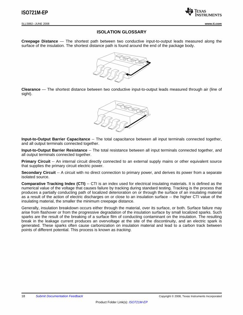
Creepage Distance — The shortest path between two conductive input-to-output leads measured along thesurface of the insulation. The shortest distance path is found around the end of the package body.
Clearance — The shortest distance between two conductive input-to-output leads measured through air (line ofsight).
Input-to-Output Barrier Capacitance -- The total capacitance between all input terminals connected together,and all output terminals connected together.
Input-to-Output Barrier Resistance -- The total resistance between all input terminals connected together, andall output terminals connected together.
Primary Circuit -- An internal circuit directly connected to an external supply mains or other equivalent sourcethat supplies the primary circuit electric power.
Secondary Circuit -- A circuit with no direct connection to primary power, and derives its power from a separateisolated source.
Comparative Tracking Index (CTI) -- CTI is an index used for electrical insulating materials. It is defined as thenumerical value of the voltage that causes failure by tracking during standard testing. Tracking is the process thatproduces a partially conducting path of localized deterioration on or through the surface of an insulating materialas a result of the action of electric discharges on or close to an insulation surface -- the higher CTI value of theinsulating material, the smaller the minimum creepage distance.
Generally, insulation breakdown occurs either through the material, over its surface, or both. Surface failure mayarise from flashover or from the progressive degradation of the insulation surface by small localized sparks. Suchsparks are the result of the breaking of a surface film of conducting contaminant on the insulation. The resultingbreak in the leakage current produces an overvoltage at the site of the discontinuity, and an electric spark isgenerated. These sparks often cause carbonization on insulation material and lead to a carbon track betweenpoints of different potential. This process is known as tracking.
Operational insulation -- Insulation needed for the correct operation of the equipment.
Basic insulation -- Insulation to provide basic protection against electric shock.
Supplementary insulation -- Independent insulation applied in addition to basic insulation in order to ensureprotection against electric shock in the event of a failure of the basic insulation.
Double insulation -- Insulation comprising both basic and supplementary insulation.
Reinforced insulation -- A single insulation system which provides a degree of protection against electric shockequivalent to double insulation.
Pollution Degree 1 -- No pollution, or only dry, nonconductive pollution occurs. The pollution has no influence.
Pollution Degree 2 -- Normally, only nonconductive pollution occurs. However, a temporary conductivity causedby condensation must be expected.
Pollution Degree 3 -- Conductive pollution occurs or dry nonconductive pollution occurs, which becomesconductive due to condensation that is to be expected.
Pollution Degree 4 – Continuous conductivity occurs due to conductive dust, rain, or other wet conditions.
Overvoltage Category -- This section is directed at insulation co-ordination by identifying the transientovervoltages that may occur, and by assigning four different levels as indicated in IEC 60664.
1. Signal Level -- Special equipment or parts of equipment.2. Local Level -- Portable equipment etc.3. Distribution Level -- Fixed installation4. Primary Supply Level -- Overhead lines, cable systems
Each category should be subject to smaller transients than the category above.
ISO721MMDREP ACTIVE SOIC D 8 2500 Green (RoHS& no Sb/Br)
CU NIPDAU Level-1-260C-UNLIM -55 to 125 721MEP
ISO721MMDREPG4 ACTIVE SOIC D 8 2500 Green (RoHS& no Sb/Br)
CU NIPDAU Level-1-260C-UNLIM -55 to 125 721MEP
V62/08627-01XE ACTIVE SOIC D 8 2500 Green (RoHS& no Sb/Br)
CU NIPDAU Level-1-260C-UNLIM -55 to 125 721MEP
(1) The marketing status values are defined as follows:ACTIVE: Product device recommended for new designs.LIFEBUY: TI has announced that the device will be discontinued, and a lifetime-buy period is in effect.NRND: Not recommended for new designs. Device is in production to support existing customers, but TI does not recommend using this part in a new design.PREVIEW: Device has been announced but is not in production. Samples may or may not be available.OBSOLETE: TI has discontinued the production of the device.
(2) Eco Plan - The planned eco-friendly classification: Pb-Free (RoHS), Pb-Free (RoHS Exempt), or Green (RoHS & no Sb/Br) - please check http://www.ti.com/productcontent for the latest availabilityinformation and additional product content details.TBD: The Pb-Free/Green conversion plan has not been defined.Pb-Free (RoHS): TI's terms "Lead-Free" or "Pb-Free" mean semiconductor products that are compatible with the current RoHS requirements for all 6 substances, including the requirement thatlead not exceed 0.1% by weight in homogeneous materials. Where designed to be soldered at high temperatures, TI Pb-Free products are suitable for use in specified lead-free processes.Pb-Free (RoHS Exempt): This component has a RoHS exemption for either 1) lead-based flip-chip solder bumps used between the die and package, or 2) lead-based die adhesive used betweenthe die and leadframe. The component is otherwise considered Pb-Free (RoHS compatible) as defined above.Green (RoHS & no Sb/Br): TI defines "Green" to mean Pb-Free (RoHS compatible), and free of Bromine (Br) and Antimony (Sb) based flame retardants (Br or Sb do not exceed 0.1% by weightin homogeneous material)
(3) MSL, Peak Temp. -- The Moisture Sensitivity Level rating according to the JEDEC industry standard classifications, and peak solder temperature.
(4) Multiple Top-Side Markings will be inside parentheses. Only one Top-Side Marking contained in parentheses and separated by a "~" will appear on a device. If a line is indented then it is acontinuation of the previous line and the two combined represent the entire Top-Side Marking for that device.
Important Information and Disclaimer:The information provided on this page represents TI's knowledge and belief as of the date that it is provided. TI bases its knowledge and belief on informationprovided by third parties, and makes no representation or warranty as to the accuracy of such information. Efforts are underway to better integrate information from third parties. TI has taken andcontinues to take reasonable steps to provide representative and accurate information but may not have conducted destructive testing or chemical analysis on incoming materials and chemicals.TI and TI suppliers consider certain information to be proprietary, and thus CAS numbers and other limited information may not be available for release.
In no event shall TI's liability arising out of such information exceed the total purchase price of the TI part(s) at issue in this document sold by TI to Customer on an annual basis.
Texas Instruments Incorporated and its subsidiaries (TI) reserve the right to make corrections, enhancements, improvements and otherchanges to its semiconductor products and services per JESD46, latest issue, and to discontinue any product or service per JESD48, latestissue. Buyers should obtain the latest relevant information before placing orders and should verify that such information is current andcomplete. All semiconductor products (also referred to herein as “components”) are sold subject to TI’s terms and conditions of salesupplied at the time of order acknowledgment.TI warrants performance of its components to the specifications applicable at the time of sale, in accordance with the warranty in TI’s termsand conditions of sale of semiconductor products. Testing and other quality control techniques are used to the extent TI deems necessaryto support this warranty. Except where mandated by applicable law, testing of all parameters of each component is not necessarilyperformed.TI assumes no liability for applications assistance or the design of Buyers’ products. Buyers are responsible for their products andapplications using TI components. To minimize the risks associated with Buyers’ products and applications, Buyers should provideadequate design and operating safeguards.TI does not warrant or represent that any license, either express or implied, is granted under any patent right, copyright, mask work right, orother intellectual property right relating to any combination, machine, or process in which TI components or services are used. Informationpublished by TI regarding third-party products or services does not constitute a license to use such products or services or a warranty orendorsement thereof. Use of such information may require a license from a third party under the patents or other intellectual property of thethird party, or a license from TI under the patents or other intellectual property of TI.Reproduction of significant portions of TI information in TI data books or data sheets is permissible only if reproduction is without alterationand is accompanied by all associated warranties, conditions, limitations, and notices. TI is not responsible or liable for such altereddocumentation. Information of third parties may be subject to additional restrictions.Resale of TI components or services with statements different from or beyond the parameters stated by TI for that component or servicevoids all express and any implied warranties for the associated TI component or service and is an unfair and deceptive business practice.TI is not responsible or liable for any such statements.Buyer acknowledges and agrees that it is solely responsible for compliance with all legal, regulatory and safety-related requirementsconcerning its products, and any use of TI components in its applications, notwithstanding any applications-related information or supportthat may be provided by TI. Buyer represents and agrees that it has all the necessary expertise to create and implement safeguards whichanticipate dangerous consequences of failures, monitor failures and their consequences, lessen the likelihood of failures that might causeharm and take appropriate remedial actions. Buyer will fully indemnify TI and its representatives against any damages arising out of the useof any TI components in safety-critical applications.In some cases, TI components may be promoted specifically to facilitate safety-related applications. With such components, TI’s goal is tohelp enable customers to design and create their own end-product solutions that meet applicable functional safety standards andrequirements. Nonetheless, such components are subject to these terms.No TI components are authorized for use in FDA Class III (or similar life-critical medical equipment) unless authorized officers of the partieshave executed a special agreement specifically governing such use.Only those TI components which TI has specifically designated as military grade or “enhanced plastic” are designed and intended for use inmilitary/aerospace applications or environments. Buyer acknowledges and agrees that any military or aerospace use of TI componentswhich have not been so designated is solely at the Buyer's risk, and that Buyer is solely responsible for compliance with all legal andregulatory requirements in connection with such use.TI has specifically designated certain components as meeting ISO/TS16949 requirements, mainly for automotive use. In any case of use ofnon-designated products, TI will not be responsible for any failure to meet ISO/TS16949.
Products ApplicationsAudio www.ti.com/audio Automotive and Transportation www.ti.com/automotiveAmplifiers amplifier.ti.com Communications and Telecom www.ti.com/communicationsData Converters dataconverter.ti.com Computers and Peripherals www.ti.com/computersDLP® Products www.dlp.com Consumer Electronics www.ti.com/consumer-appsDSP dsp.ti.com Energy and Lighting www.ti.com/energyClocks and Timers www.ti.com/clocks Industrial www.ti.com/industrialInterface interface.ti.com Medical www.ti.com/medicalLogic logic.ti.com Security www.ti.com/securityPower Mgmt power.ti.com Space, Avionics and Defense www.ti.com/space-avionics-defenseMicrocontrollers microcontroller.ti.com Video and Imaging www.ti.com/videoRFID www.ti-rfid.comOMAP Applications Processors www.ti.com/omap TI E2E Community e2e.ti.comWireless Connectivity www.ti.com/wirelessconnectivity