133
03/25/22 ECE250 (KEH) 1
| Date post: | 21-Dec-2015 |
| Category: |
Documents |
| View: | 220 times |
| Download: | 0 times |

04/18/23 ECE250 (KEH) 1

04/18/23 ECE250 (KEH) 2
Introduction to Bipolar Junction Transistors
(Read Chapter 3 of Text)

04/18/23 ECE250 (KEH) 3
Bipolar Junction Transistor
• Current-controlled current source• Made by sandwiching thin N-type Si
between two P-type Si (PNP BJT)• Or by sandwiching thin P-type Si between
two N-type Si (NPN BJT)• Leads called Base (B), Collector (C) and
Emitter (E). Control current “IB” flows from B to E. Resulting current “IC” is “pumped” from C to E.

04/18/23 ECE250 (KEH) 4
NPN and PNP BJTs
04/18/23 ECE250 (KEH) 5
Integrated Circuit NPN BJT
The previous slide implied that the C and E leads are interchangeable, but it can be seen above that the emitter (E) is doped more heavily (n++) than the collector region (n), and the collector (C) surrounds the base region (p+), while E is a small button. The doping levels for E, B, and C regions are 1019, 1017 and 1015 cm-3, respectively. Note the aluminum contact to the collector “n-type Si” region is made using an “n++” diffusion so that the contact is “ohmic” rather than a rectifying Schottky diode.
04/18/23 ECE250 (KEH) 6
NPN BJT is biased in “Forward Active” mode when B-E pn junction is forward biased and B-C pn
junction is reverse biased.
04/18/23 ECE250 (KEH) 7
Electron Current in Forward-Active NPN BJT
Electrons from the highly-doped emitter “n++” region are injected into base region through the forward-biased BE junction. They diffuse through the VERY THIN base region, with only a few of these electrons having a chance to recombine with holes in the thin “p+” base region. The vast majority of the injected electrons (perhaps α ≈ 0.99 of the injected electrons) diffuse to the edge of the base region near the reverse-biased BC junction, where the intense electric field associated with the reverse-biased BC junction (directed from N to P regions) sweeps these electrons into the “n” collector region, where they constitute collector current. The remaining “1- α”= 1 – 0.99 ≈ 0.01 of the injected electrons that recombine with holes in the base region constitute a portion of the small base current “Ib1”.
N++ P+ N

04/18/23 ECE250 (KEH) 8
Hole Current in Forward-Active NPN BJT
We shall see that the electron current diffusing across the forward-biased B-E junction from E to B regions, as discussed on the previous slide, results in desirable transistor action. However, the hole current that flows from B to E region adds an UNDESIRED contribution “Ib2” to the total base current, Ib = Ib1 + Ib2. We desire that the total base current “Ib” be as small as possible for a given collector current “Ic”. This results in a “forward current transfer ratio” (current gain) βF = Ic / Ib that is as large as possible. The undesired hole current component of Ib (Ib2) is made negligibly small by doping the E region heavily (n++) and the base region about 100 times less heavily than the B region (p+).
04/18/23 ECE250 (KEH) 9
Relationship between Emitter, Base, and Collector Current in a Forward-Active BJT
• IE = Is*exp(VBE/VT), since the BE junction is forward-biased. (Note η = 1 for IC BJTs.)
• IC = α*IE, because α ≈ 0.99 of the electrons injected into the THIN base region diffuse across the base and get swept across the reverse-biased BC junction.
• IB = (1- α)*IE, because the remaining (1- α) ≈ 0.01 of the electrons recombine with holes in the base region.
04/18/23 ECE250 (KEH) 10
Relating β to α• αF, the “forward current transfer ratio” is defined
as the ratio of collector to emitter current in a forward-active BJT Note: IC/IE = αF*IE / IE = αF
• βF, the “transistor current gain” is defined as the collector current divided by the controlling base current in a forward-active BJT.
• Note βF = IC/IB = αF*IE / (1- αF)*IE = αF/(1- αF)• Thus if αF = 0.99, βF = 0.99/(1-0.99) = 99• The subscript “F” is often dropped, if it is clear
that we are talking about a forward-active BJT.
04/18/23 ECE250 (KEH) 11
NPN BJT in “Common Emitter” Configuration
Voltage source VBB forward-biases BE junction (assuming VBB > 0.7V), making VBE ≈ 0.7 V.
Voltage source VCC reverse-biases BC junction. Thus BJT is biased into its “forward-active” region, and
IB = (VBB – 0.7V)/RB, IC = βFIB, and IE = IC + IB = (βF+1) IB

04/18/23 ECE250 (KEH) 12
Operating Modes of NPN BJT
1. If VBB < 0.7 V, both BE and BC junctions are OFF, and BJT is “cut off”. No currents flow in a cut off BJT IC = IE = IB = 0. The terminals of the BJT are essentially “open-circuited”.
2. If VBB > 0.7 V, VCC > 0.1 V, BE junction is forward-biased, and BC junction is reverse-biased. So BJT is forward active, where IC = βIB.
3. If, while in forward-active mode, VBB is increased to a point where VCE = VCC – βFIBRC falls below about 0.1V, VBE = 0.7V (on hard) and VBC = VBE – VCE = 0.7V – 0.1V = 0.6V, and thus the BC junction turns on (lightly). Under this condition the BJT is said to be saturated. IC no longer = βFIB. Instead, the BE junction acts like a 0.7 V battery and the BC junction acts like a 0.6 V battery.
04/18/23 ECE250 (KEH) 13
4. Reverse Active Mode (BC fwd-biased, BE rev-biased)
• If C and E terminals are interchanged in the circuit above, it would at first seem that the circuit will function exactly as it did before due to the apparent symmetry of the BJT. Now the BC junction will be forward-biased and the BE junction will be reverse-biased.
• However, we learned earlier that a modern BJT is NOT symmetric, since the C and E regions are different shape, and the doping level in the E region is much higher (n++) than the doping level in the C region (n).
• Thus with C and E interchanged, the BJT operates in reverse active mode, which is similar to forward active mode, except the roles of IE and IC have been interchanged, and now the undesired hole current component of Ib (Ib2) is much larger and more injected electrons recombine in the base region, thereby reducing the forward transfer current ratio well below 1. Now αR ~ 0.5, and now βR = αR /(1- αR ) ~ 1.
• Now IE = βR IB and IC = (βR +1)IB, since the roles of C and E are reversed.
Change this to E
Change this to C
Keep the B connection the same

04/18/23 ECE250 (KEH) 14
Electron and Hole Currents in a Forward-Active PNP BJT
Ic = αF*IE IC = βFIB IE= (βF+1)IB
Forward Active PNP BJT has SAME equations as before, just opposite current and voltage polarities! As before, BE junction is forward biased and BC junction is reverse biased. Now (VEB)on = 0.7 V.
04/18/23 ECE250 (KEH) 15
NPN and PNP BJT SymbolsNote that emitter arrow indicates reference direction of
emitter current, IE

04/18/23 ECE250 (KEH) 16
Summary of NPN and BJT Fwd Active Equations
04/18/23 ECE250 (KEH) 17
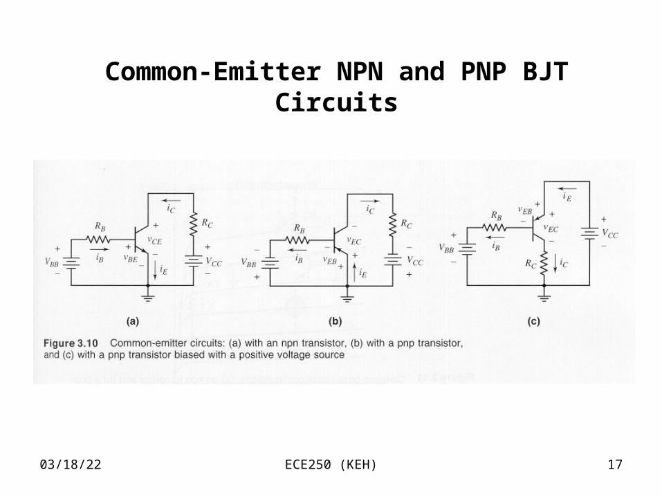
Common-Emitter NPN and PNP BJT Circuits

04/18/23 ECE250 (KEH) 18
Typical I vs V “Family of Curves” for the Common-Emitter NPN BJT Circuit
(Ideally, each curve should be horizontal, so IC = βFIB for any VCE > 0.1V)

04/18/23 ECE250 (KEH) 19
Non-Ideality Parameters for the BJT: VA and BVCEO
04/18/23 ECE250 (KEH) 20
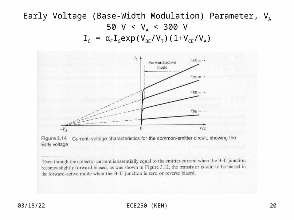
Early Voltage (Base-Width Modulation) Parameter, VA
50 V < VA < 300 VIC = αFISexp(VBE/VT)(1+VCE/VA)
04/18/23 ECE250 (KEH) 21
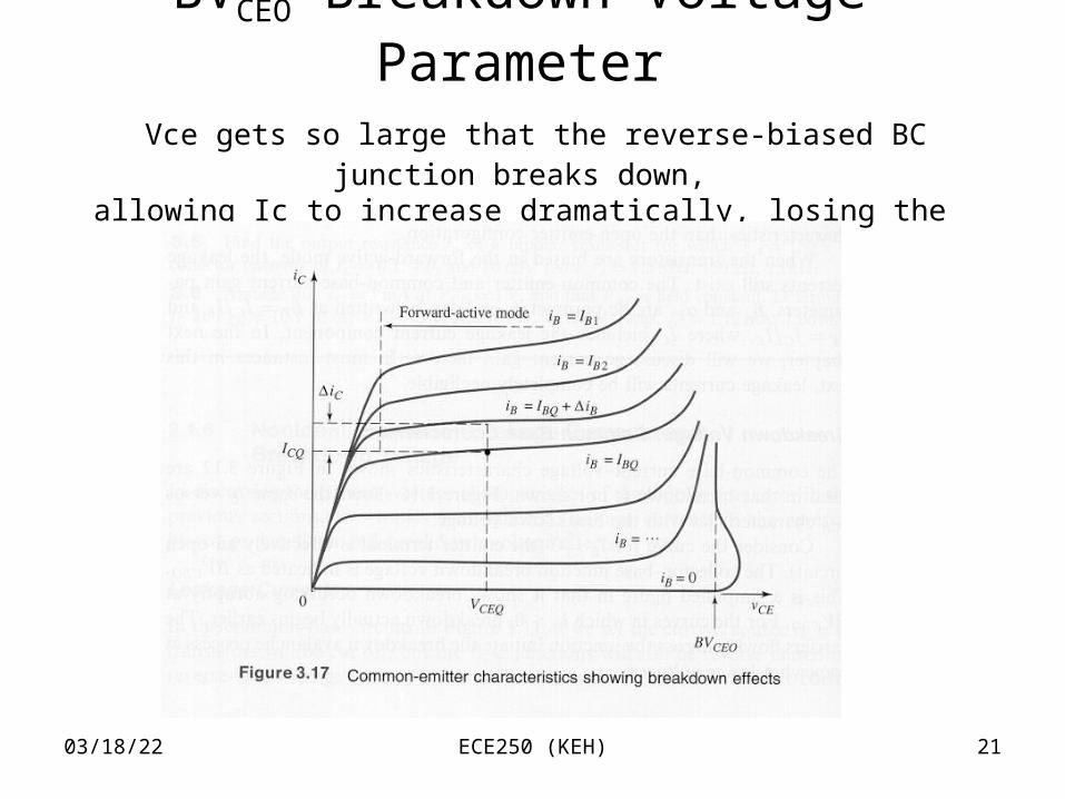
BVCEO Breakdown Voltage Parameter Vce gets so large that the reverse-biased BC junction breaks down,allowing Ic to increase dramatically, losing the IC=βFIB amplifying effect.
04/18/23 ECE250 (KEH) 22
DC Equivalent Forward-Active Model of NPN BJT
04/18/23 ECE250 (KEH) 23
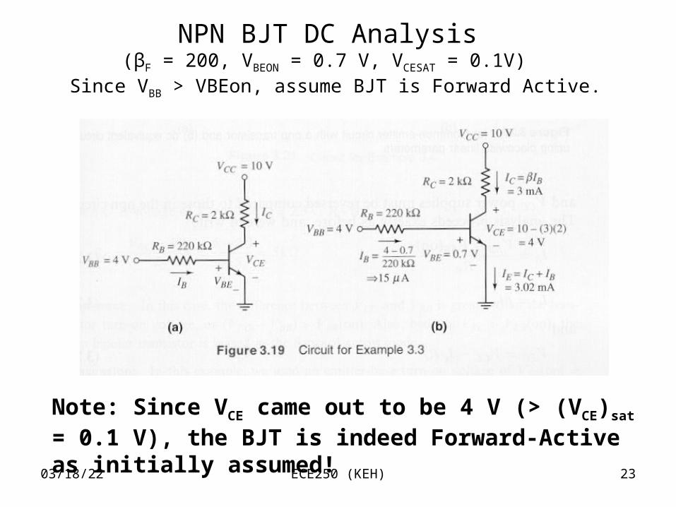
NPN BJT DC Analysis (βF = 200, VBEON = 0.7 V, VCESAT = 0.1V)
Since VBB > VBEon, assume BJT is Forward Active.
Note: Since VCE came out to be 4 V (> (VCE)sat = 0.1 V), the BJT is indeed Forward-Active as initially assumed!
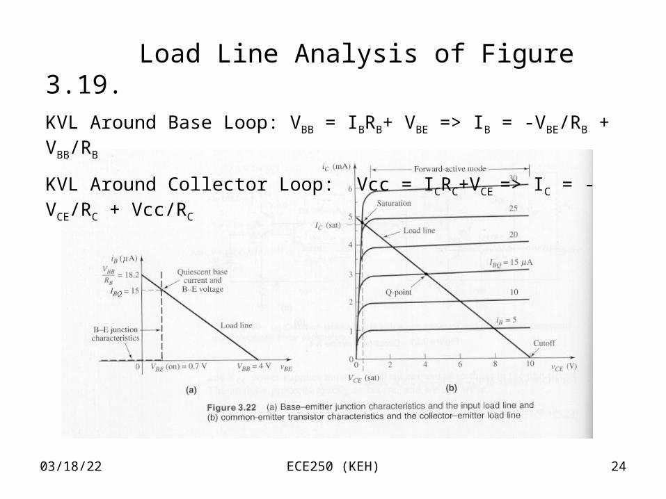
04/18/23 ECE250 (KEH) 24
Load Line Analysis of Figure 3.19.KVL Around Base Loop: VBB = IBRB+ VBE => IB = -VBE/RB + VBB/RB
KVL Around Collector Loop: Vcc = ICRC+VCE => IC = -VCE/RC + Vcc/RC
04/18/23 ECE250 (KEH) 25
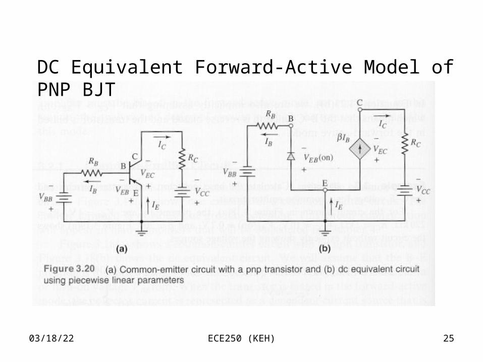
DC Equivalent Forward-Active Model of PNP BJT
04/18/23 ECE250 (KEH) 26
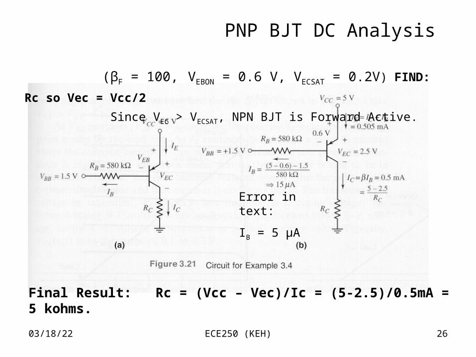
PNP BJT DC Analysis (βF = 100, VEBON = 0.6 V, VECSAT = 0.2V) FIND: Rc so Vec = Vcc/2 Since VEC > VECSAT, NPN BJT is Forward Active.
Final Result: Rc = (Vcc – Vec)/Ic = (5-2.5)/0.5mA = 5 kohms.
Error in text:
IB = 5 μA
04/18/23 ECE250 (KEH) 27
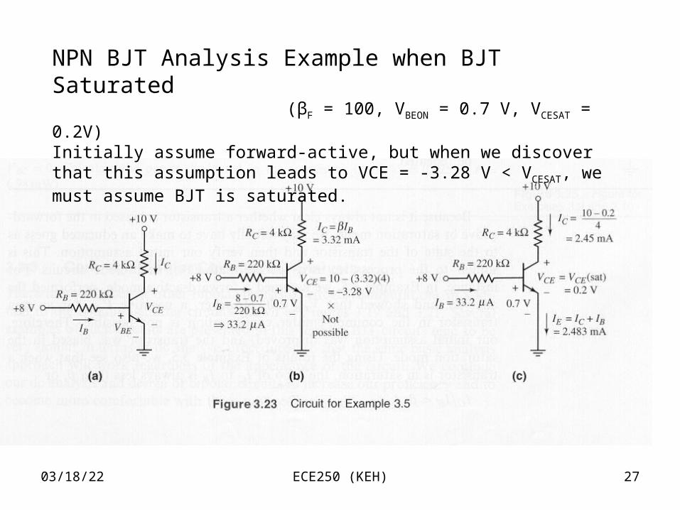
NPN BJT Analysis Example when BJT Saturated (βF = 100, VBEON = 0.7 V, VCESAT = 0.2V)Initially assume forward-active, but when we discover that this assumption leads to VCE = -3.28 V < VCESAT, we must assume BJT is saturated.
04/18/23 ECE250 (KEH) 28
04/18/23 ECE250 (KEH) 29
04/18/23 ECE250 (KEH) 30
04/18/23 ECE250 (KEH) 31
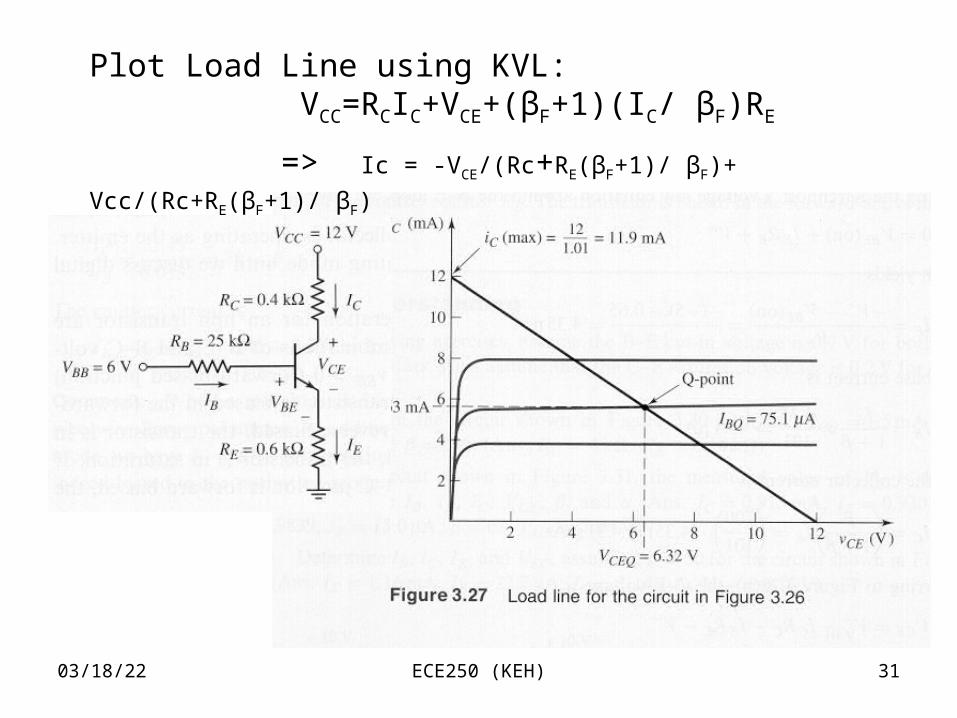
Plot Load Line using KVL: VCC=RCIC+VCE+(βF+1)(IC/ βF)RE
=> Ic = -VCE/(Rc+RE(βF+1)/ βF)+ Vcc/(Rc+RE(βF+1)/ βF)
04/18/23 ECE250 (KEH) 32
04/18/23 ECE250 (KEH) 33
04/18/23 ECE250 (KEH) 34
04/18/23 ECE250 (KEH) 35
04/18/23 ECE250 (KEH) 36
04/18/23 ECE250 (KEH) 37
04/18/23 ECE250 (KEH) 38
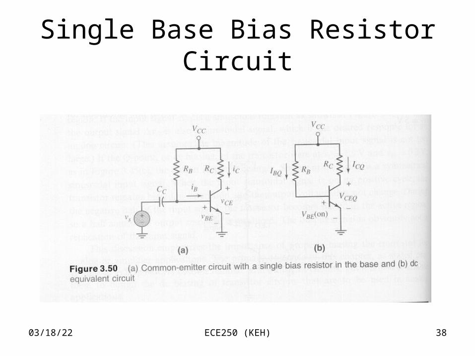
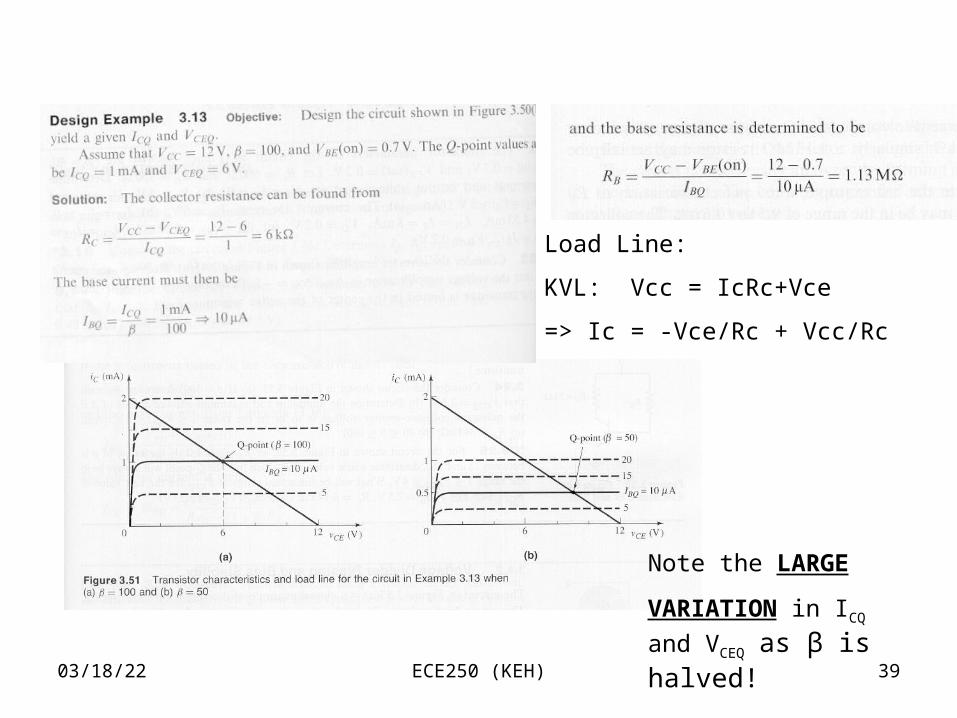
Single Base Bias Resistor Circuit
04/18/23 ECE250 (KEH) 39
Load Line:
KVL: Vcc = IcRc+Vce
=> Ic = -Vce/Rc + Vcc/Rc
Note the LARGE
VARIATION in ICQ and
VCEQ as β is halved!
04/18/23 ECE250 (KEH) 40
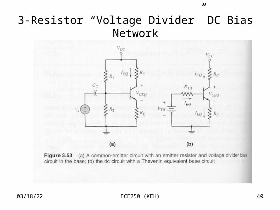
3-Resistor “Voltage Divider” DC Bias Network
04/18/23 ECE250 (KEH) 41
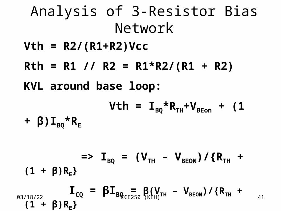
Analysis of 3-Resistor Bias Network
Vth = R2/(R1+R2)Vcc
Rth = R1 // R2 = R1*R2/(R1 + R2)
KVL around base loop:
Vth = IBQ*RTH+VBEon + (1 + β)IBQ*RE
=> IBQ = (VTH – VBEON)/{RTH + (1 + β)RE}
ICQ = βIBQ = β(VTH – VBEON)/{RTH + (1 + β)RE}
04/18/23 ECE250 (KEH) 42
Design for “Bias Stability” w.r.t. β
Solution: For the 3-resistor bias network, we found on the previous slide
ICQ = β(VTH - VBEon)/{RTH + (1+ β)RE}If we make RTH << (1+ β)RE then
ICQ ≈β(VTH - VBEon)/(1+ β)RE
Since β /(1+ β) ≈ 1 (since β is typically > 100)
ICQ ≈(VTH - VBEon)/RE
Thus we can make ICQ approximately independent of β variation,
simply by choosing component values so that
(1+ β)RE = 10RTH
Problem: β varies over a wide range. For the 2N2222, 80 < β < 300). How do we keep the dc bias current and voltage from changing as β changes?

04/18/23 ECE250 (KEH) 43
BJT Common-Emitter (CE) Audio Amplifier Analysis and Design
We will start with the complete circuit of a CE amplifier, then we will proceed to
its DC model to find its Q-point (Icq, Vceq), then its AC model to find its
input resistance, output resistance, and its small-signal gain Av = vout(t) / vin(t)
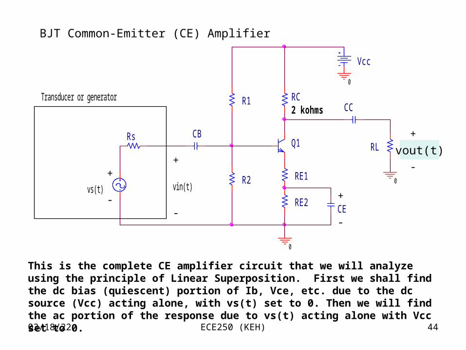
04/18/23 ECE250 (KEH) 44
BJT Common-Emitter (CE) Amplifier
R1
R2
vo(t)
0
RE2
Transducer or generator
+
CBRs
vin(t)
0
CC2 kohms
-
+
vs(t)
RL
Vcc
CE
RC
+
-RE1
+
-
-
0
Q1
This is the complete CE amplifier circuit that we will analyze using the principle of Linear Superposition. First we shall find the dc bias (quiescent) portion of Ib, Vce, etc. due to the dc source (Vcc) acting alone, with vs(t) set to 0. Then we will find the ac portion of the response due to vs(t) acting alone with Vcc set to 0.
vout(t)

04/18/23 ECE250 (KEH) 45
DC Bias Point Design Problem
In a design problem, you are given the desired Q-point, and
you must choose the component values needed to “make this Q-point happen”

04/18/23 ECE250 (KEH) 46
We shall follow two “design rules of thumb” to promote bias stability:
1. Choose component values so that (β + 1)RE >> RTH, Let us make
(β + 1)RE = 10RTH
2. VE should be the same order of magnitude as Vbe(on), so we let us make
VE = 1.0 V.
04/18/23 ECE250 (KEH) 47
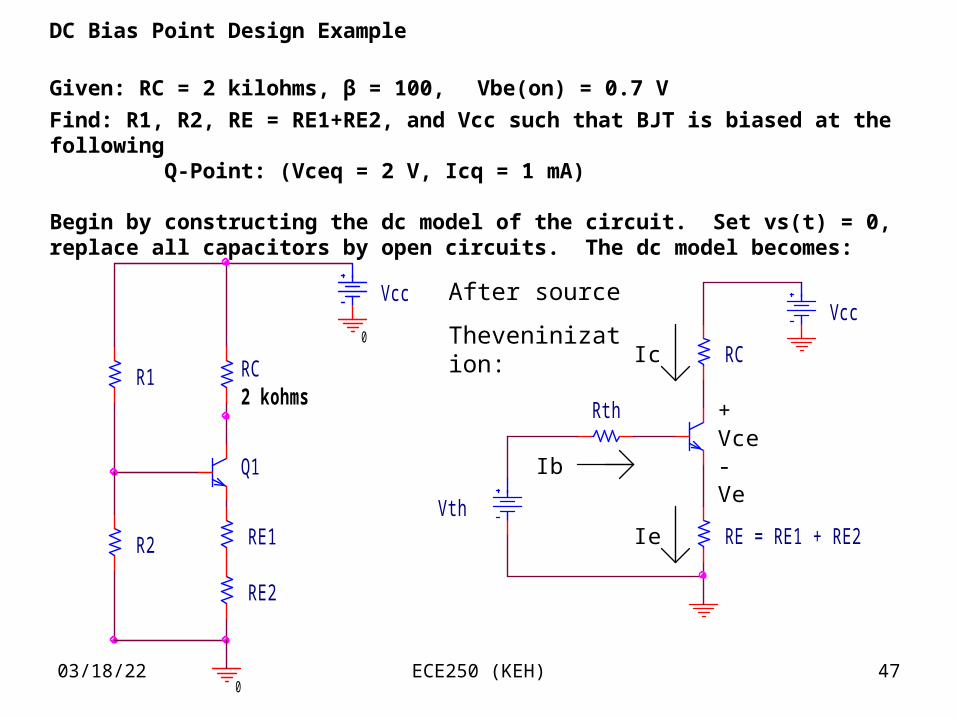
DC Bias Point Design Example
Given: RC = 2 kilohms, β = 100, Vbe(on) = 0.7 V
Find: R1, R2, RE = RE1+RE2, and Vcc such that BJT is biased at the following Q-Point: (Vceq = 2 V, Icq = 1 mA)
Begin by constructing the dc model of the circuit. Set vs(t) = 0, replace all capacitors by open circuits. The dc model becomes:
RE1
0
0
Vcc
2 kohms
Q1
R1
R2
RE2
RCIc
Rth +
RE = RE1 + RE2
RC
-
Vth
Vcc
Ve
VceIb
Ie
After source
Theveninization:
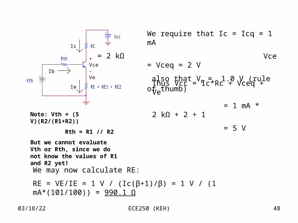
04/18/23 ECE250 (KEH) 48
Ic
Rth +
RE = RE1 + RE2
RC
-
Vth
Vcc
Ve
VceIb
Ie
We require that Ic = Icq = 1 mA
Vce = Vceq = 2 V
also that VE = 1.0 V (rule of thumb)
Thus Vcc = Ic*Rc + Vceq + Ve
= 1 mA * 2 kΩ + 2 + 1
= 5 V
= 2 kΩ
Note: Vth = (5 V)(R2/(R1+R2))
Rth = R1 // R2
But we cannot evaluate Vth or Rth, since we do not know the values of R1 and R2 yet!
We may now calculate RE:
RE = VE/IE = 1 V / (Ic(β+1)/β) = 1 V / (1 mA*(101/100)) = 990.1 Ω
04/18/23 ECE250 (KEH) 49
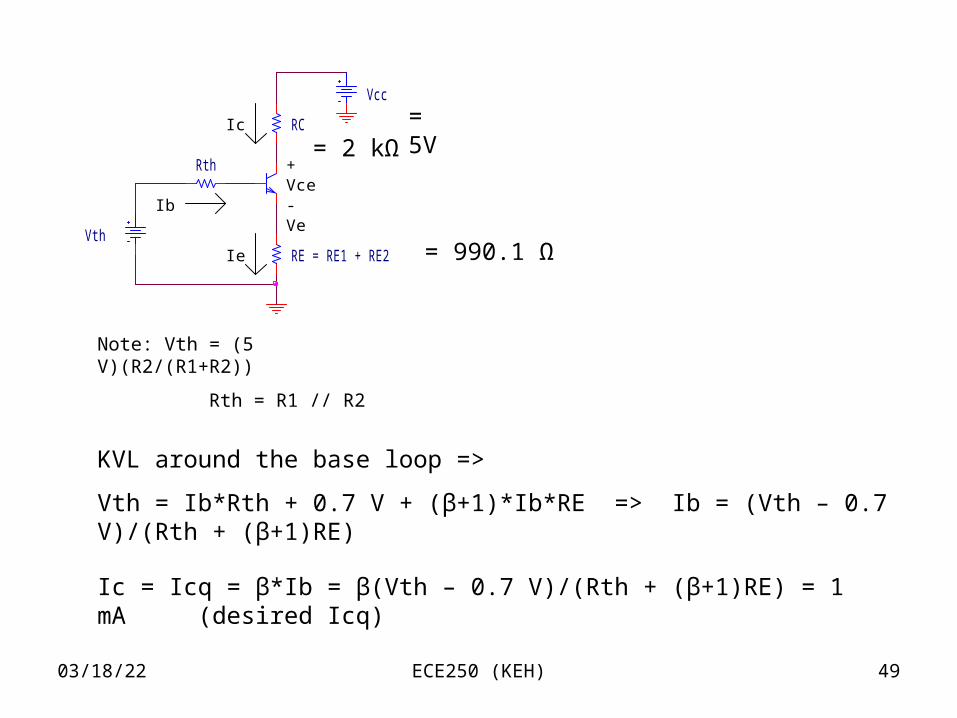
Ic
Rth +
RE = RE1 + RE2
RC
-
Vth
Vcc
Ve
VceIb
Ie
= 2 kΩ
Note: Vth = (5 V)(R2/(R1+R2))
Rth = R1 // R2
= 5V
= 990.1 Ω
KVL around the base loop =>
Vth = Ib*Rth + 0.7 V + (β+1)*Ib*RE => Ib = (Vth – 0.7 V)/(Rth + (β+1)RE)
Ic = Icq = β*Ib = β(Vth – 0.7 V)/(Rth + (β+1)RE) = 1 mA (desired Icq)
04/18/23 ECE250 (KEH) 50
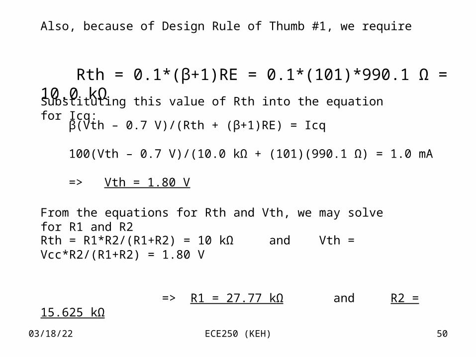
Also, because of Design Rule of Thumb #1, we require
Rth = 0.1*(β+1)RE = 0.1*(101)*990.1 Ω = 10.0 kΩ
β(Vth – 0.7 V)/(Rth + (β+1)RE) = Icq
100(Vth – 0.7 V)/(10.0 kΩ + (101)(990.1 Ω) = 1.0 mA
=> Vth = 1.80 V
Substituting this value of Rth into the equation for Icq:
From the equations for Rth and Vth, we may solve for R1 and R2
Rth = R1*R2/(R1+R2) = 10 kΩ and Vth = Vcc*R2/(R1+R2) = 1.80 V
=> R1 = 27.77 kΩ and R2 = 15.625 kΩ
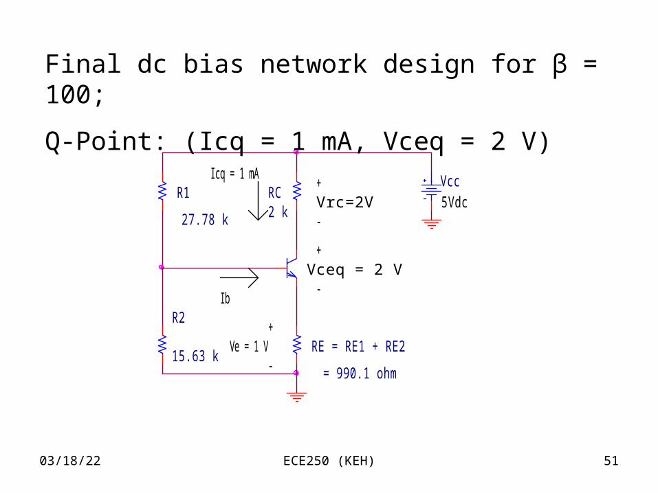
04/18/23 ECE250 (KEH) 51
Vrc=2V
Ve = 1 V+
+
+
-
-
-
Vceq = 2 V
RE = RE1 + RE2
= 990.1 ohm
Vcc5Vdc
IbR2
15.63 k
R1
27.78 k
RC2 k
Icq = 1 mA
Final dc bias network design for β = 100;
Q-Point: (Icq = 1 mA, Vceq = 2 V)

04/18/23 ECE250 (KEH) 52
DC Bias Point Analysis Example Problem
In an analysis problem, all of the component values are given, and you
are to find the resulting Q-point
04/18/23 ECE250 (KEH) 53
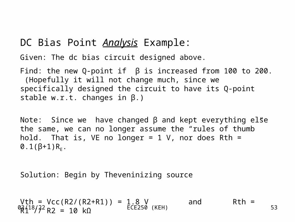
DC Bias Point Analysis Example:
Given: The dc bias circuit designed above.
Find: the new Q-point if β is increased from 100 to 200. (Hopefully it will not change much, since we specifically designed the circuit to have its Q-point stable w.r.t. changes in β.)
Note: Since we have changed β and kept everything else the same, we can no longer assume the “rules of thumb” hold. That is, VE no longer = 1 V, nor does Rth = 0.1(β+1)RE.
Solution: Begin by Theveninizing source
Vth = Vcc(R2/(R2+R1)) = 1.8 V and Rth = R1 // R2 = 10 kΩ
04/18/23 ECE250 (KEH) 54
Vceq = 2 V
RE = RE1 + RE2
= 990.1 ohm
-
Rth
10 kIb
RC2 k
Ic
+
Vcc5Vdc
Vth
1.8 V
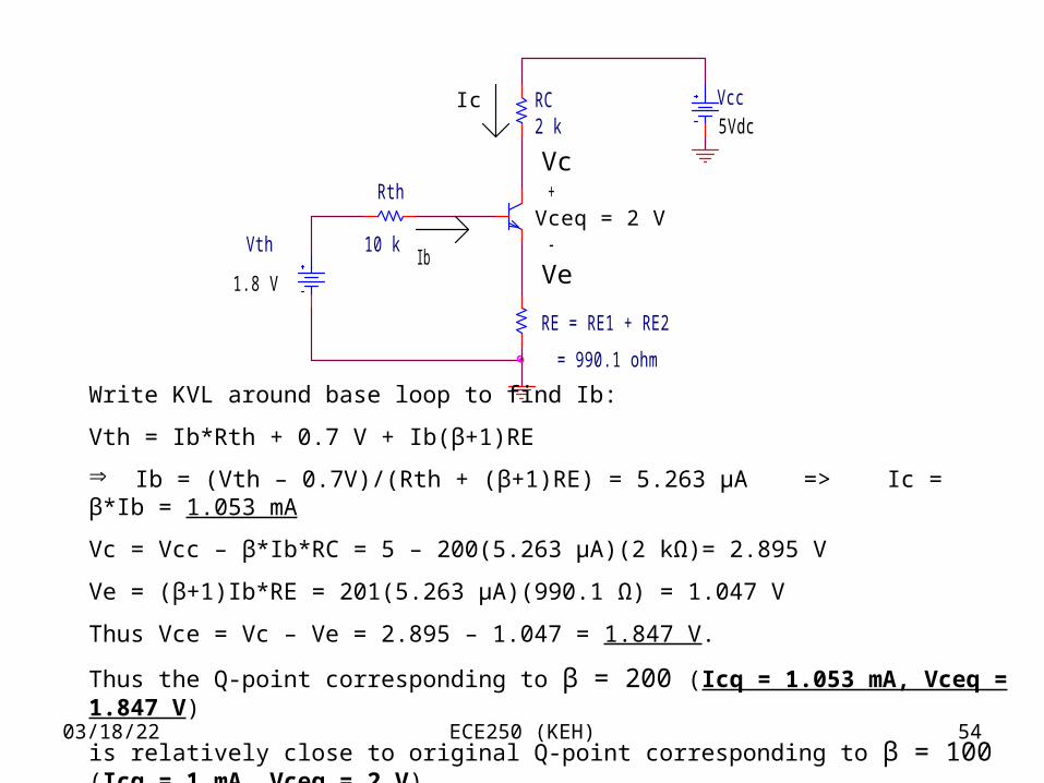
Write KVL around base loop to find Ib:
Vth = Ib*Rth + 0.7 V + Ib(β+1)RE
Ib = (Vth – 0.7V)/(Rth + (β+1)RE) = 5.263 µA => Ic = β*Ib = 1.053 mA
Vc = Vcc – β*Ib*RC = 5 – 200(5.263 µA)(2 kΩ)= 2.895 V
Ve = (β+1)Ib*RE = 201(5.263 µA)(990.1 Ω) = 1.047 V
Thus Vce = Vc – Ve = 2.895 – 1.047 = 1.847 V.
Thus the Q-point corresponding to β = 200 (Icq = 1.053 mA, Vceq = 1.847 V)
is relatively close to original Q-point corresponding to β = 100 (Icq = 1 mA, Vceq = 2 V)
Vc
Ve
04/18/23 ECE250 (KEH) 55
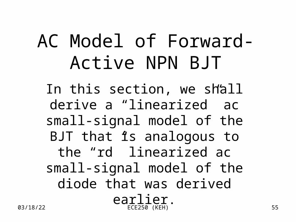
AC Model of Forward-Active NPN BJT
In this section, we shall derive a “linearized” ac small-signal model of the BJT that is analogous to the
“rd” linearized ac small-signal model of the diode that was
derived earlier.
04/18/23 ECE250 (KEH) 56
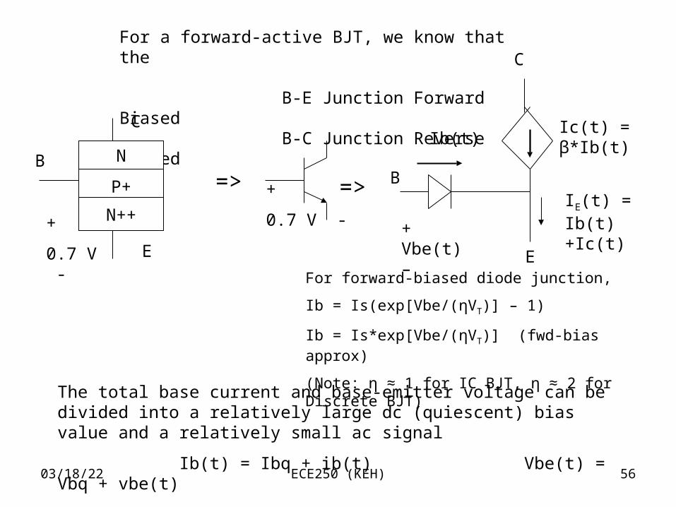
For a forward-active BJT, we know that the
B-E Junction Forward Biased B-C Junction Reverse Biased
N
P+
N++
C
B
E
+
0.7 V -
=> +
0.7 V -
=>
Ic(t) = β*Ib(t)
C
E
B
+ Vbe(t) –
Ib(t)
For forward-biased diode junction,
Ib = Is(exp[Vbe/(ηVT)] – 1)
Ib = Is*exp[Vbe/(ηVT)] (fwd-bias approx)
(Note: η ≈ 1 for IC BJT, η ≈ 2 for Discrete BJT)
The total base current and base-emitter voltage can be divided into a relatively large dc (quiescent) bias value and a relatively small ac signal
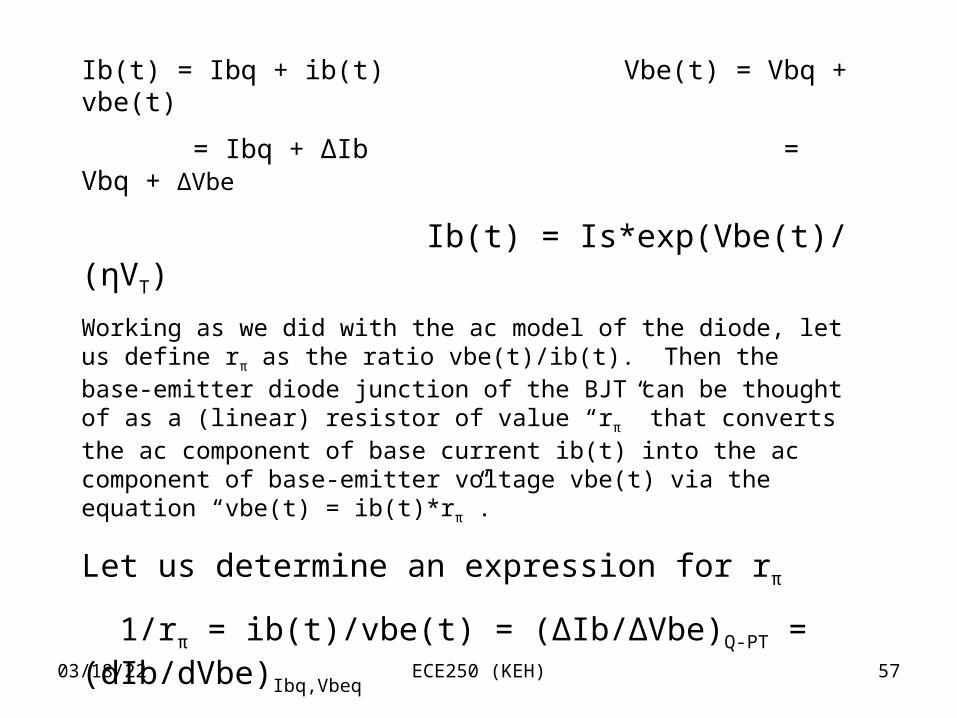
Ib(t) = Ibq + ib(t) Vbe(t) = Vbq + vbe(t)
IE(t) = Ib(t)+Ic(t)
04/18/23 ECE250 (KEH) 57
Ib(t) = Ibq + ib(t) Vbe(t) = Vbq + vbe(t)
= Ibq + ΔIb = Vbq + ΔVbe
Ib(t) = Is*exp(Vbe(t)/ (ηVT)
Working as we did with the ac model of the diode, let us define rπ as the ratio vbe(t)/ib(t). Then the base-emitter diode junction of the BJT can be thought of as a (linear) resistor of value “rπ” that converts the ac component of base current ib(t) into the ac component of base-emitter voltage vbe(t) via the equation “vbe(t) = ib(t)*rπ”.
Let us determine an expression for rπ
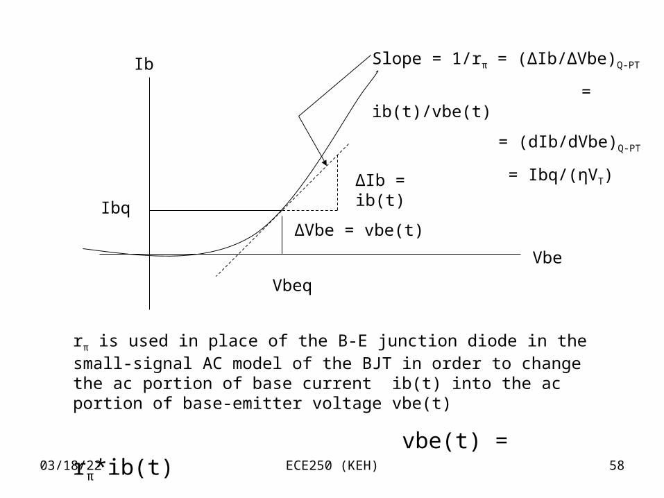
1/rπ = ib(t)/vbe(t) = (ΔIb/ΔVbe)Q-PT = (dIb/dVbe)Ibq,Vbeq
= (1/(ηVT)* Is*exp(Vbe(t)/ (ηVT))Q-PT
= (1/(ηVT))*Ib)Q-PT = Ibq/(ηVT)
04/18/23 ECE250 (KEH) 58
Vbeq
Ibq
Ib
Vbe
ΔIb = ib(t)
ΔVbe = vbe(t)
Slope = 1/rπ = (ΔIb/ΔVbe)Q-PT
= ib(t)/vbe(t)
= (dIb/dVbe)Q-PT
= Ibq/(ηVT)
rπ is used in place of the B-E junction diode in the small-signal AC model of the BJT in order to change the ac portion of base current ib(t) into the ac portion of base-emitter voltage vbe(t)
vbe(t) = rπ*ib(t)
04/18/23 ECE250 (KEH) 59
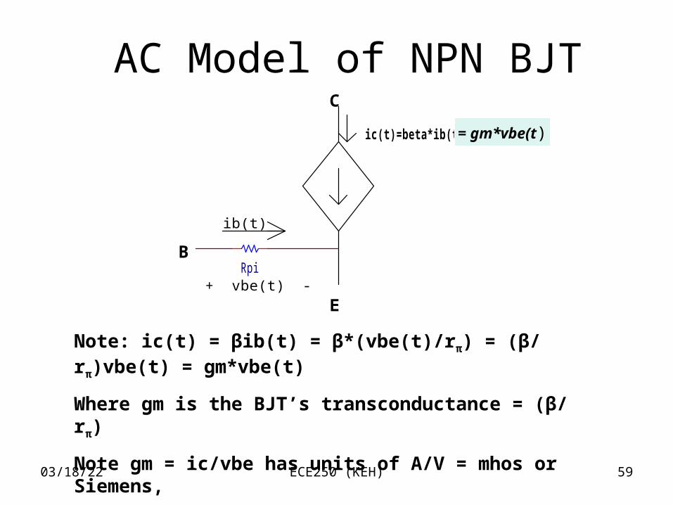
AC Model of NPN BJT
RpiB
E
ib(t)
+ vbe(t) -
C
ic(t)=beta*ib(t) = gm*vbe(t)
Note: ic(t) = βib(t) = β*(vbe(t)/rπ) = (β/ rπ)vbe(t) = gm*vbe(t)
Where gm is the BJT’s transconductance = (β/ rπ)
Note gm = ic/vbe has units of A/V = mhos or Siemens,
And β = ic/ib which makes it a unitless quantity.
= gm*vbe(t)
04/18/23 ECE250 (KEH) 60
AC Model of BJT Amplifier
In this section, we shall construct the ac model of the CE amplifier
circuit, and from it, we shall derive the small-signal ac voltage gain,
input impedance, output impedance, etc.
04/18/23 ECE250 (KEH) 61
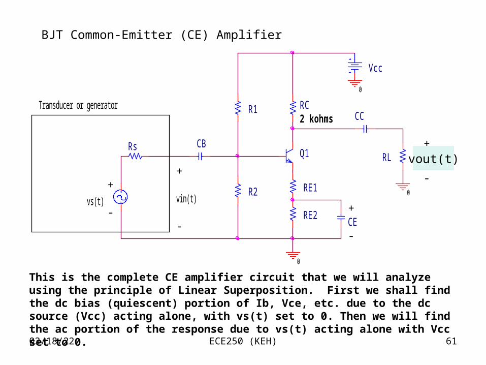
BJT Common-Emitter (CE) Amplifier
R1
R2
vo(t)
0
RE2
Transducer or generator
+
CBRs
vin(t)
0
CC2 kohms
-
+
vs(t)
RL
Vcc
CE
RC
+
-RE1
+
-
-
0
Q1
This is the complete CE amplifier circuit that we will analyze using the principle of Linear Superposition. First we shall find the dc bias (quiescent) portion of Ib, Vce, etc. due to the dc source (Vcc) acting alone, with vs(t) set to 0. Then we will find the ac portion of the response due to vs(t) acting alone with Vcc set to 0.
vout(t)
04/18/23 ECE250 (KEH) 62
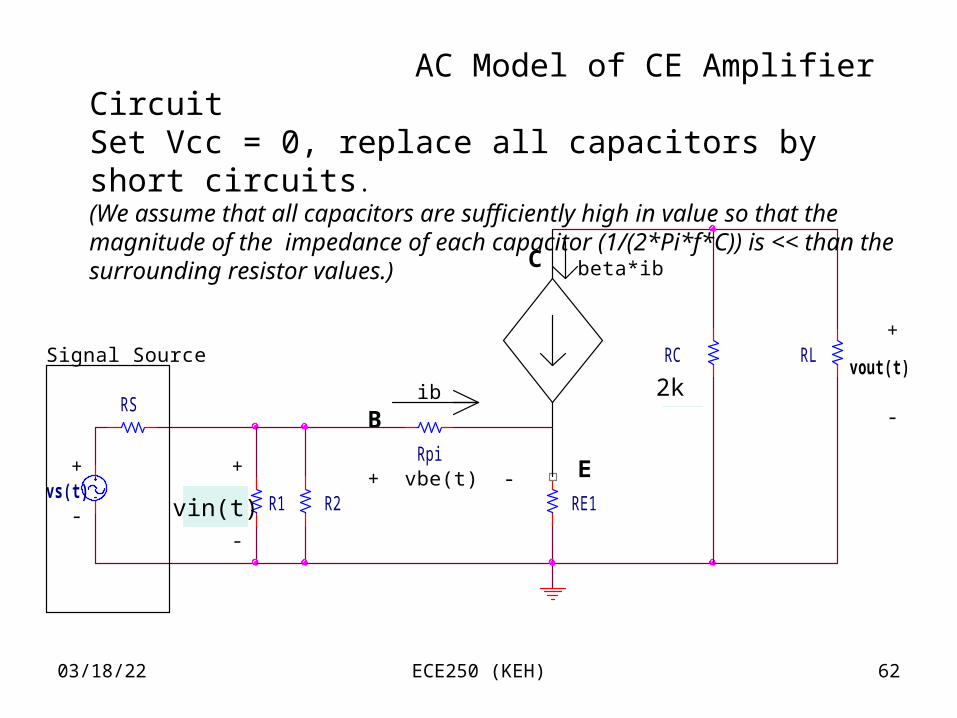
Rpi
B
vout(t)
RE1
-
vs(t)
RL
E
vi(t)
beta*ib
ib
+ vbe(t) -
RC
1k
Signal Source
RS
+
- R1
+
+
C
R2
-
AC Model of CE Amplifier CircuitSet Vcc = 0, replace all capacitors by short circuits. (We assume that all capacitors are sufficiently high in value so that the magnitude of the impedance of each capacitor (1/(2*Pi*f*C)) is << than the surrounding resistor values.)
vin(t)
2k
04/18/23 ECE250 (KEH) 63
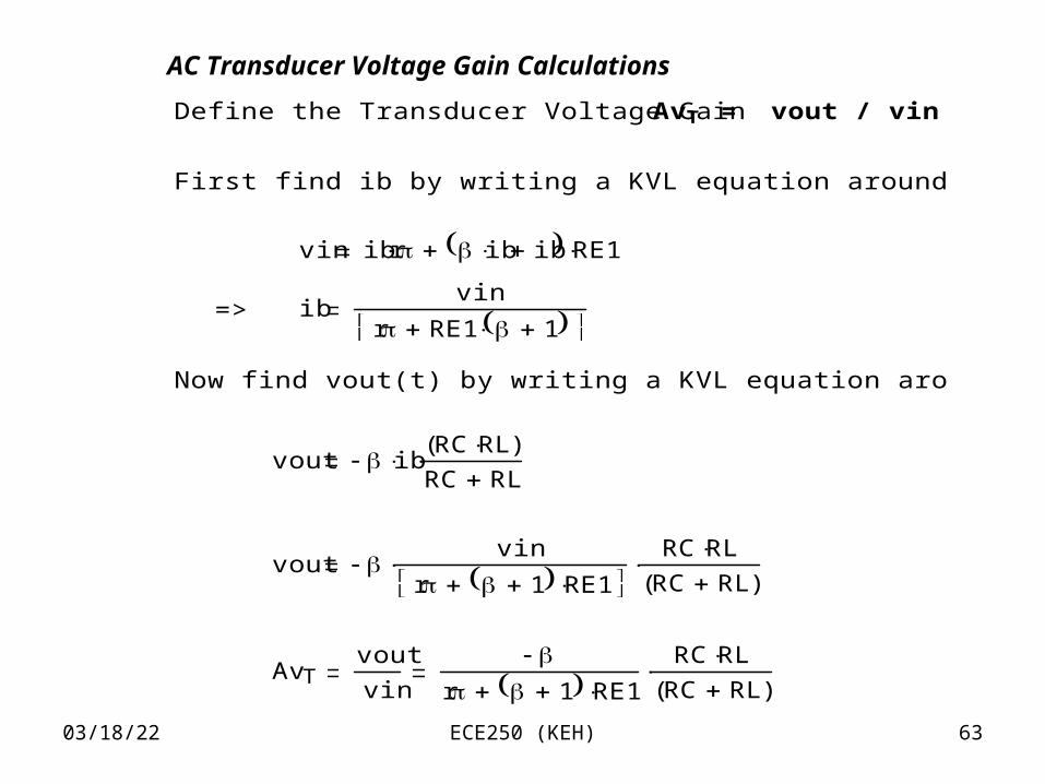
AC Transducer Voltage Gain Calculations
Define the Transducer Voltage Gain AvT = vout / vin
First find ib by writing a KVL equation around the base loop:
vin ib r ib ib RE1
=> ibvin
r RE1 1
Now find vout(t) by writing a KVL equation around the collector loop
vout ibRC RL( )
RC RL
vout vin
r 1 RE1
RC RLRC RL( )
AvTvout
vin
r 1 RE1
RC RLRC RL( )
04/18/23 ECE250 (KEH) 64
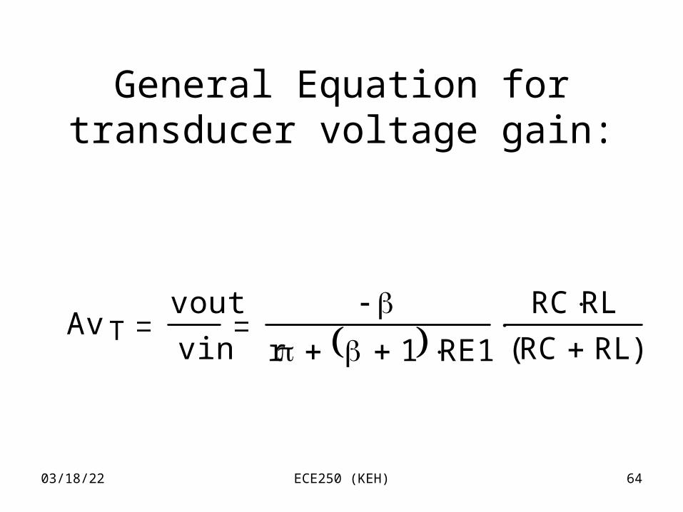
General Equation for transducer voltage gain:
Av Tvout
vin
r 1 RE1
RC RLRC RL( )
04/18/23 ECE250 (KEH) 65
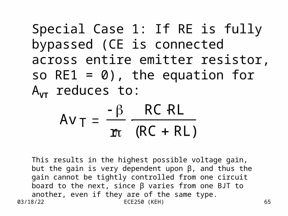
Special Case 1: If RE is fully bypassed (CE is connected across entire emitter resistor, so RE1 = 0), the equation for AVT reduces to:
Av T
r
RC RLRC RL( )
This results in the highest possible voltage gain, but the gain is very dependent upon β, and thus the gain cannot be tightly controlled from one circuit board to the next, since β varies from one BJT to another, even if they are of the same type.
04/18/23 ECE250 (KEH) 66
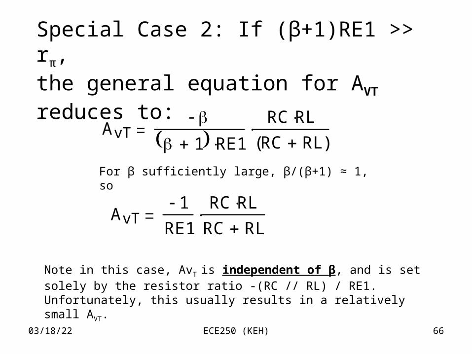
Special Case 2: If (β+1)RE1 >> rπ,the general equation for AVT reduces to:
AvT
1 RE1
RC RLRC RL( )
AvT1
RE1
RC RLRC RL
For β sufficiently large, β/(β+1) ≈ 1, so
Note in this case, AvT is independent of β, and is set solely by the resistor ratio -(RC // RL) / RE1. Unfortunately, this usually results in a relatively small AVT.
04/18/23 ECE250 (KEH) 67
In our design example, let RL = 4 kΩ
Given:
2 (This is a discrete BJT) low 100 high 200
R1 27.78 k R2 15.63 k RC 2 k RL 4 k
Find AC model B-E resistance "r" for =100 and for :
r100 26 mV1.0 mA
low
r100 5.2 103
r200 26 mV1.053 mA
high
r200 9.877 103
04/18/23 ECE250 (KEH) 68
Case 1: Fully Bypassed Case (CE across entire RE)
=> RE2 990.1 RE1 0
AvT200high
r200 high 1 RE1
RC RLRC RL( )
AvT200 27
AvT100low
r100 low 1 RE1
RC RLRC RL( )
AvT100 25.641
04/18/23 ECE250 (KEH) 69
Case 2: Partially Bypassed Case (CE across all but 50 ohms of RE)
=> RE2 940.1 RE1 50
AvT200high
r200 high 1 RE1
RC RLRC RL( )
AvT200 13.382
AvT100low
r100 low 1 RE1
RC RLRC RL( )
AvT100 13.008
04/18/23 ECE250 (KEH) 70
Case 3: Unbypassed Case (CE not present)
=> RE2 0 RE1 990.1
AvT200high
r200 high 1 RE1
RC RLRC RL( )
AvT200 1.277
AvT100low
r100 low 1 RE1
RC RLRC RL( )
AvT100 1.267
04/18/23 ECE250 (KEH) 71
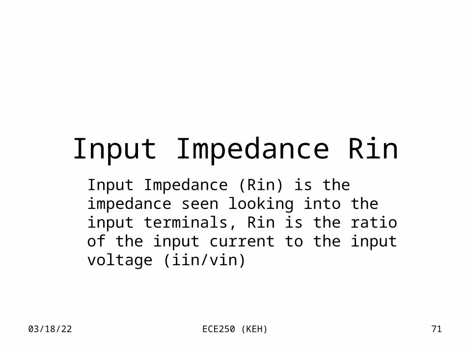
Input Impedance RinInput Impedance (Rin) is the impedance seen looking into the input terminals, Rin is the ratio of the input current to the input voltage (iin/vin)
04/18/23 ECE250 (KEH) 72
Rpi
B
vout(t)
RE1
-
vs(t)
RL
E
vi(t)
beta*ib
ib
+ vbe(t) -
RC
1k
Signal Source
RS
+
- R1
+
+
C
R2
-
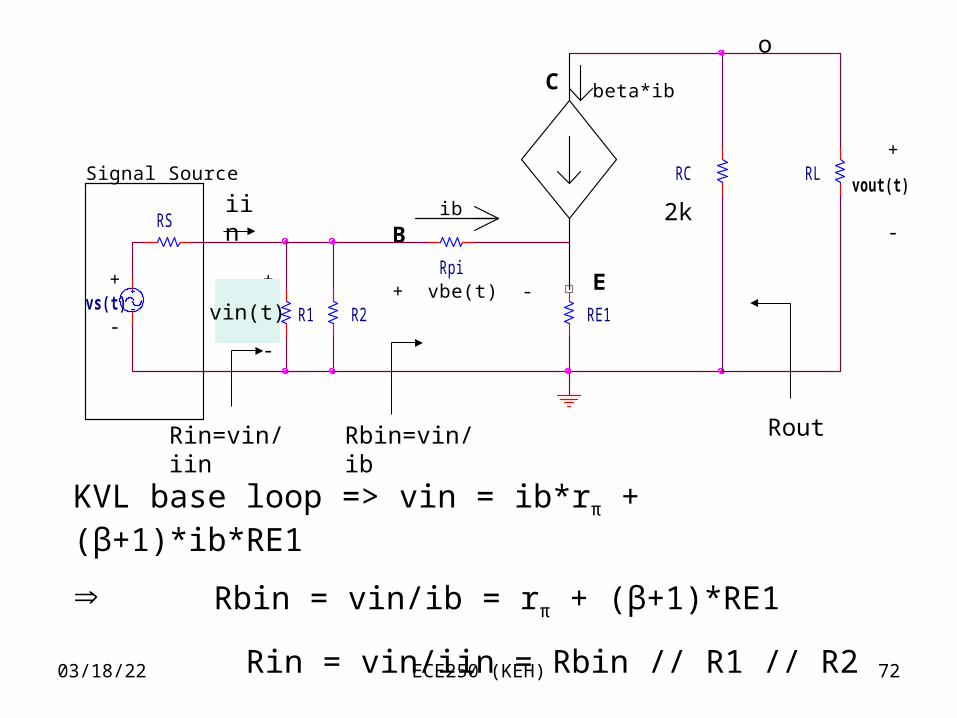
Rin=vin/iin
iin
Rbin=vin/ib Rout
KVL base loop => vin = ib*rπ + (β+1)*ib*RE1
Rbin = vin/ib = rπ + (β+1)*RE1
Rin = vin/iin = Rbin // R1 // R2
vin(t)
o
2k
04/18/23 ECE250 (KEH) 73
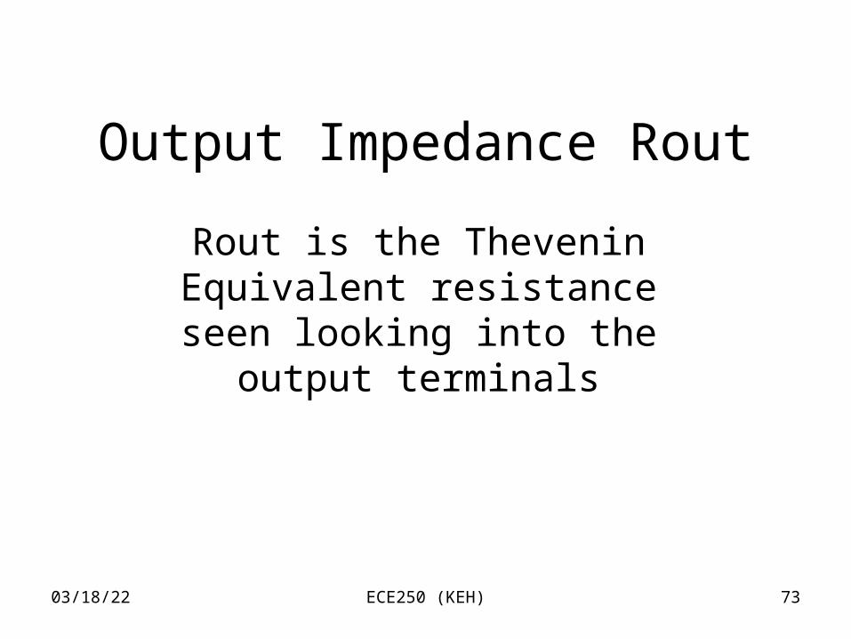
Output Impedance Rout
Rout is the Thevenin Equivalent resistance seen looking into the
output terminals
04/18/23 ECE250 (KEH) 74
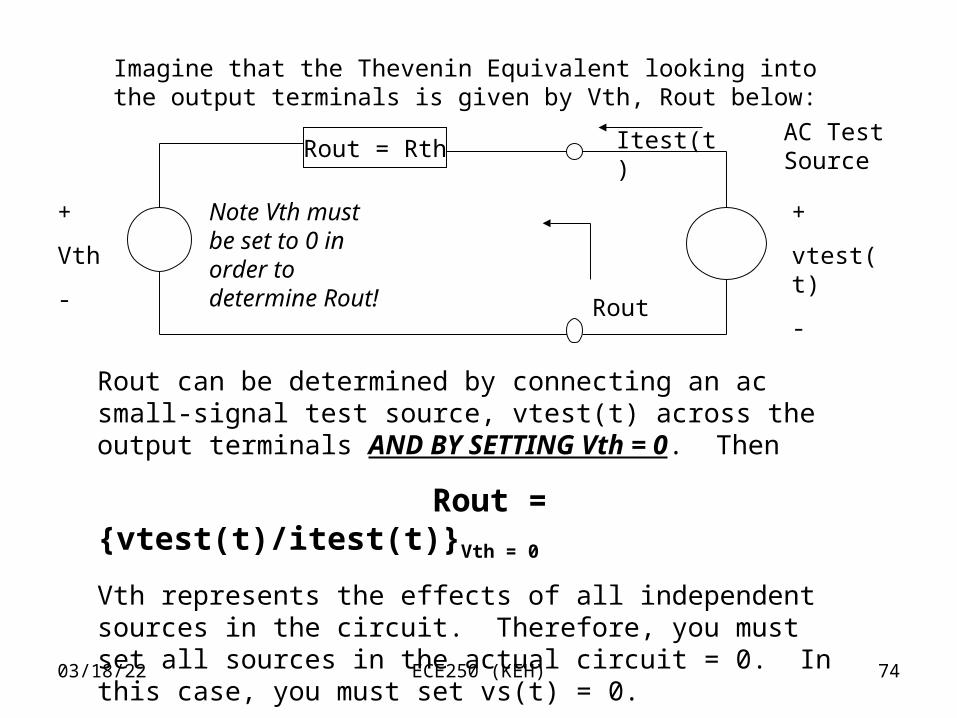
Imagine that the Thevenin Equivalent looking into the output terminals is given by Vth, Rout below:
Rout = Rth
+
Vth
-
AC Test Source
+
vtest(t)
-
Itest(t)
Rout can be determined by connecting an ac small-signal test source, vtest(t) across the output terminals AND BY SETTING Vth = 0. Then
Rout = {vtest(t)/itest(t)}Vth = 0
Vth represents the effects of all independent sources in the circuit. Therefore, you must set all sources in the actual circuit = 0. In this case, you must set vs(t) = 0.
Rout
Note Vth must be set to 0 in order to determine Rout!
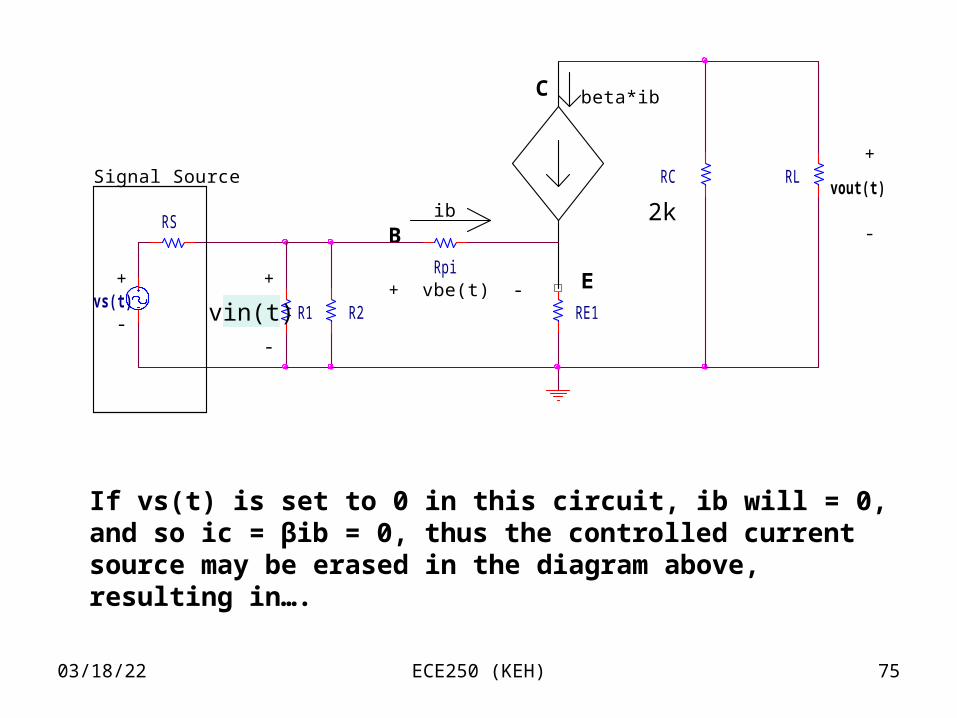
04/18/23 ECE250 (KEH) 75
If vs(t) is set to 0 in this circuit, ib will = 0, and so ic = βib = 0, thus the controlled current source may be erased in the diagram above, resulting in….
Rpi
B
vout(t)
RE1
-
vs(t)
RL
E
vi(t)
beta*ib
ib
+ vbe(t) -
RC
1k
Signal Source
RS
+
- R1
+
+
C
R2
-
vin(t)
2k
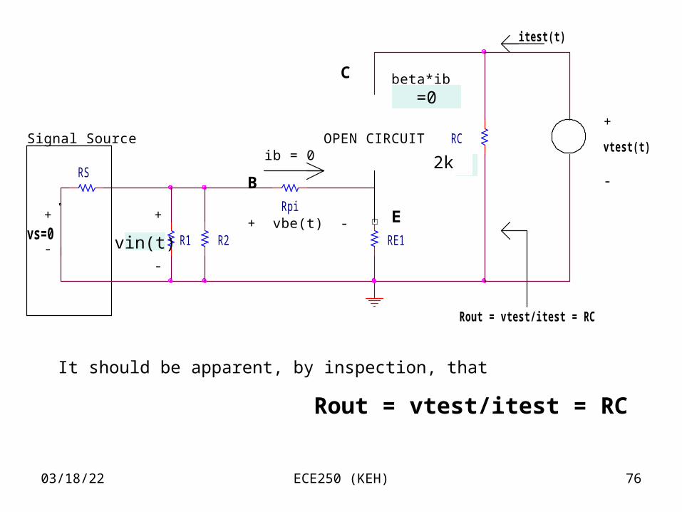
04/18/23 ECE250 (KEH) 76
It should be apparent, by inspection, that
Rout = vtest/itest = RC
C
-
Signal Sourcevtest(t)
+ vbe(t) -
RC
1k
R1
ib = 0
+
B
vi(t)vs=0
itest(t)
RE1
OPEN CIRCUIT
R2
RS
Rout = vtest/itest = RC
-
+
beta*ib
+
-
RpiE
vin(t)
=0
2k
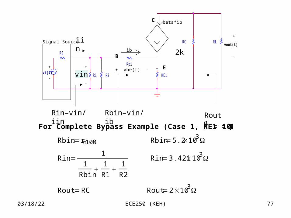
04/18/23 ECE250 (KEH) 77
Rpi
B
vout(t)
RE1
-
vs(t)
RL
E
vi(t)
beta*ib
ib
+ vbe(t) -
RC
1k
Signal Source
RS
+
- R1
+
+
C
R2
-
Rin=vin/iin
iin
Rbin=vin/ib RoutFor Complete Bypass Example (Case 1, RE1 = 0, = 100)
Rbin r100 Rbin 5.2 103
Rin1
1
Rbin
1
R1
1
R2
Rin 3.421 103
Rout RC Rout 2 103
vin
2k
04/18/23 ECE250 (KEH) 78
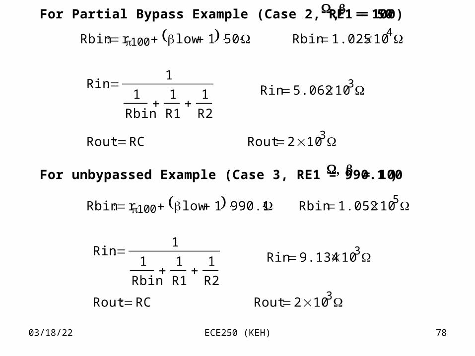
For Partial Bypass Example (Case 2, RE1 = 50 , = 100)
Rbin r100 low 1 50 Rbin 1.025 104
Rin1
1
Rbin
1
R1
1
R2
Rin 5.062 103
Rout RC Rout 2 103
For unbypassed Example (Case 3, RE1 = 990.1 = 100)
Rbin r100 low 1 990.1 Rbin 1.052 105
Rin1
1
Rbin
1
R1
1
R2
Rin 9.134 103
Rout RC Rout 2 103
04/18/23 ECE250 (KEH) 79
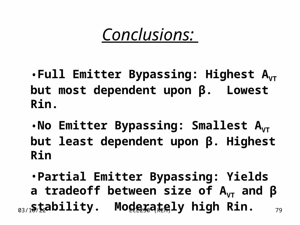
Conclusions:
•Full Emitter Bypassing: Highest AVT but most dependent upon β. Lowest Rin.
•No Emitter Bypassing: Smallest AVT but least dependent upon β. Highest Rin
•Partial Emitter Bypassing: Yields a tradeoff between size of AVT and β stability. Moderately high Rin.
04/18/23 ECE250 (KEH) 80
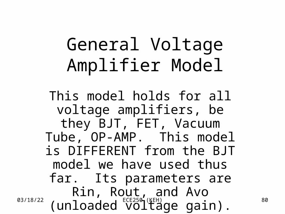
General Voltage Amplifier Model
This model holds for all voltage amplifiers, be they BJT, FET,
Vacuum Tube, OP-AMP. This model is DIFFERENT from the
BJT model we have used thus far. Its parameters are Rin, Rout, and
Avo (unloaded voltage gain).
04/18/23 ECE250 (KEH) 81
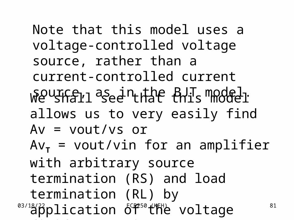
Note that this model uses a voltage-controlled voltage source, rather than a current-controlled current source, as in the BJT model.
We shall see that this model allows us to very easily find Av = vout/vs or AvT = vout/vin for an amplifier with arbitrary source termination (RS) and load termination (RL) by application of the voltage divider equation.
04/18/23 ECE250 (KEH) 82
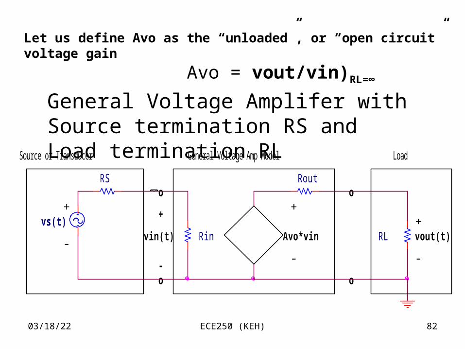
Let us define Avo as the “unloaded”, or “open circuit” voltage gain
Avo = vout/vin)RL=∞
General Voltage Amplifer with Source termination RS and Load termination RL
+
Rout
General Voltage Amp Model
o
-
vout(t)+
RLRin
+vs(t)
-
o
o
RS
--
Load
Avo*vin
Source or Transducer
+
vin(t)
o
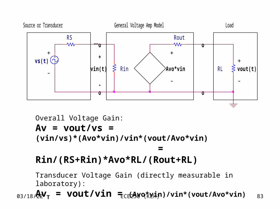
04/18/23 ECE250 (KEH) 83
Overall Voltage Gain:
Av = vout/vs = (vin/vs)*(Avo*vin)/vin*(vout/Avo*vin)
= Rin/(RS+Rin)*Avo*RL/(Rout+RL)
Transducer Voltage Gain (directly measurable in laboratory):
AvT = vout/vin = (Avo*vin)/vin*(vout/Avo*vin)
= Avo*RL/(Rout+RL)
+
Rout
General Voltage Amp Model
o
-
vout(t)+
RLRin
+vs(t)
-
o
o
RS
--
Load
Avo*vin
Source or Transducer
+
vin(t)
o
04/18/23 ECE250 (KEH) 84
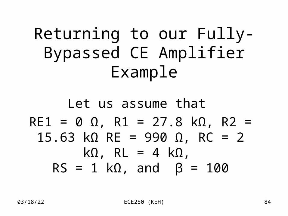
Returning to our Fully-Bypassed CE Amplifier Example
Let us assume that
RE1 = 0 Ω, R1 = 27.8 kΩ, R2 = 15.63 kΩ RE = 990 Ω, RC = 2 kΩ, RL = 4 kΩ,
RS = 1 kΩ, and β = 100
04/18/23 ECE250 (KEH) 85
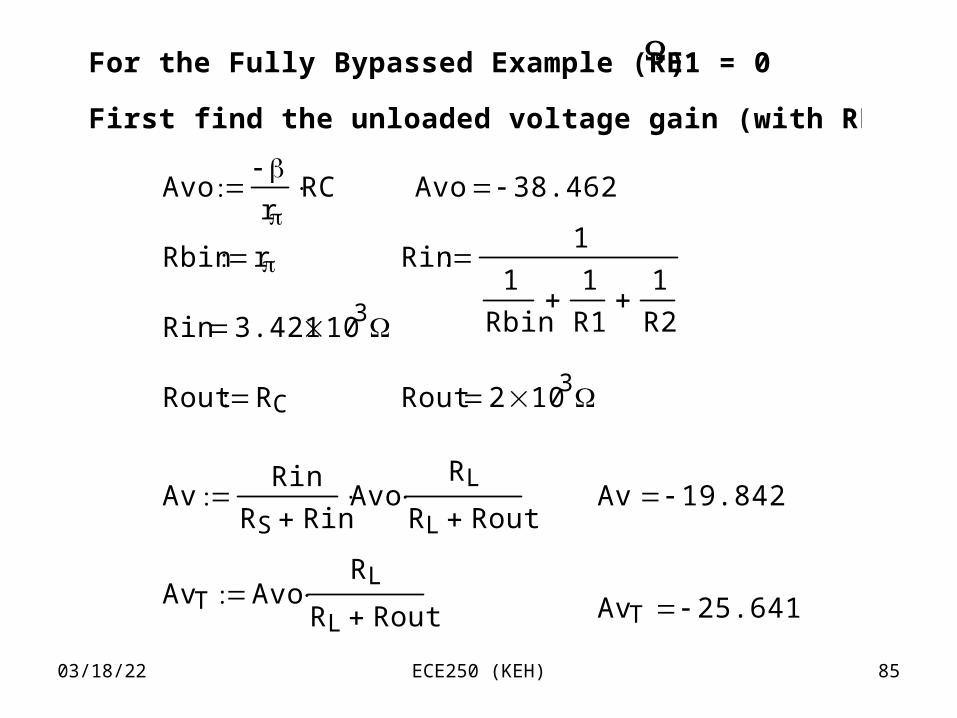
For the Fully Bypassed Example (RE1 = 0 )
First find the unloaded voltage gain (with RL set to infinity)
Avo
rRC Avo 38.462
Rbin r Rin1
1
Rbin
1
R1
1
R2
Rin 3.421 103
Rout RC Rout 2 103
AvRin
RS RinAvo
RL
RL Rout Av 19.842
AvT AvoRL
RL Rout AvT 25.641
04/18/23 ECE250 (KEH) 86
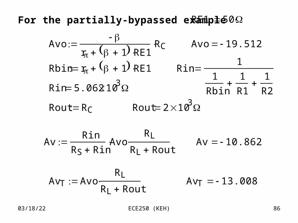
For the partially-bypassed example RE1 50
Avo
r 1 RE1RC Avo 19.512
Rbin r 1 RE1 Rin1
1
Rbin
1
R1
1
R2
Rin 5.062 103
Rout RC Rout 2 103
AvRin
RS RinAvo
RL
RL Rout Av 10.862
AvT AvoRL
RL Rout AvT 13.008
04/18/23 ECE250 (KEH) 87
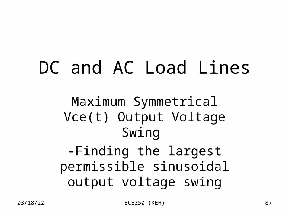
DC and AC Load Lines
Maximum Symmetrical Vce(t) Output Voltage Swing
-Finding the largest permissible sinusoidal output voltage swing
04/18/23 ECE250 (KEH) 88
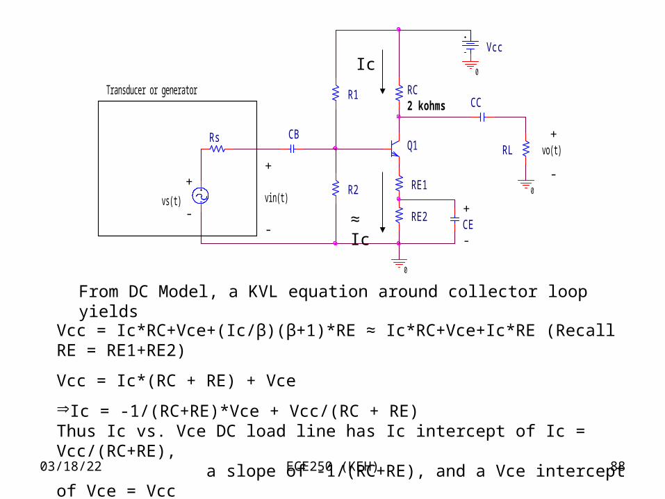
R1
R2
vo(t)
0
RE2
Transducer or generator
+
CBRs
vin(t)
0
CC2 kohms
-
+
vs(t)
RL
Vcc
CE
RC
+
-RE1
+
-
-
0
Q1
From DC Model, a KVL equation around collector loop yields
Vcc = Ic*RC+Vce+(Ic/β)(β+1)*RE ≈ Ic*RC+Vce+Ic*RE (Recall RE = RE1+RE2)
Vcc = Ic*(RC + RE) + Vce
Ic = -1/(RC+RE)*Vce + Vcc/(RC + RE)Thus Ic vs. Vce DC load line has Ic intercept of Ic = Vcc/(RC+RE), a slope of -1/(RC+RE), and a Vce intercept of Vce = Vcc
Ic
≈ Ic
04/18/23 ECE250 (KEH) 89
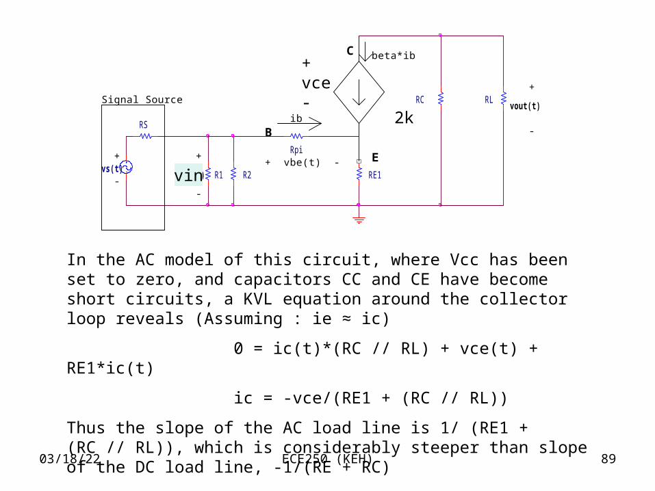
In the AC model of this circuit, where Vcc has been set to zero, and capacitors CC and CE have become short circuits, a KVL equation around the collector loop reveals (Assuming : ie ≈ ic)
0 = ic(t)*(RC // RL) + vce(t) + RE1*ic(t)
ic = -vce/(RE1 + (RC // RL))
Thus the slope of the AC load line is 1/ (RE1 + (RC // RL)), which is considerably steeper than slope of the DC load line, -1/(RE + RC)
Rpi
B
vout(t)
RE1
-
vs(t)
RL
E
vi(t)
beta*ib
ib
+ vbe(t) -
RC
1k
Signal Source
RS
+
- R1
+
+
C
R2
-
+vce-
vin
2k
04/18/23 ECE250 (KEH) 90
The AC and DC load lines must both pass through the DC bias Q-point, since the total Ic(t) and Vce(t) signals are the sum of the AC and DC signal components.
Vcc/(RC+RE)
Vcc
DC Load LineIc
Vce
AC Load Line
Q-PointIb = Ibq
Ib = Ibq + 50uA
Ib = Ibq – 50uA
VceqΔVcemax
Vce(SAT)
Icq
Slope AC Load Line = -1/((RC // RL) + RE1) = -Icq / ΔVcemax
There are TWO ways to calculate slope of AC Load Line:

04/18/23 ECE250 (KEH) 91
We may solve for ΔVcemax. For our fully-bypassed example (RE1 = 0),
ΔVcemax = Icq*((RC // RL) + RE1)
= (1 mA)*(2k // 4k) = 1.33 V
Thus the Vce(t) total (dc + ac component) output voltage signal may swing above the Q-point value “Vceq” by ΔVcemax = 1.33 V before the BJT enters cutoff and stops amplifying. Likwise, Vceq may swing below the Vceq by (Vceq – Vce(SAT)) volts = 2 – 0.2 = 1.8 V before it hits saturation and stops amplifying. Because the output voltage is typically thought to swing symmetrically (sinusoidally) about the Q-point, just as much above the Q-pt as below it, we must take the smaller of these two distances. Because
ΔVcemax = 1.33 V < (Vceq – Vce(SAT)) = 1.8 V
We take our Maximum Symmetrical Vce(t) Output Voltage Swing to be
Max. Symm Vce Swing = 2*(ΔVcemax) = 2(1.33) = 2.66 V, peak-to-peak.
If the above inequality were reversed, as it sometimes is, then
Max. Symm Vce Swing = 2*((Vceq – Vce(SAT)) (in V, peak-to-peak)
Note: Take the smaller distance and double it – since “a chain is only as strong as its weakest link”
04/18/23 ECE250 (KEH) 92
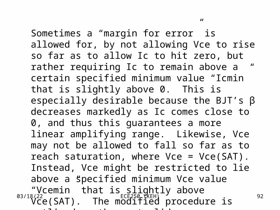
Sometimes a “margin for error” is allowed for, by not allowing Vce to rise so far as to allow Ic to hit zero, but rather requiring Ic to remain above a certain specified minimum value “Icmin” that is slightly above 0. This is especially desirable because the BJT’s β decreases markedly as Ic comes close to 0, and thus this guarantees a more linear amplifying range. Likewise, Vce may not be allowed to fall so far as to reach saturation, where Vce = Vce(SAT). Instead, Vce might be restricted to lie above a specified minimum Vce value “Vcemin” that is slightly above Vce(SAT). The modified procedure is outlined on the next slide:
04/18/23 ECE250 (KEH) 93
Vcc
DC Load LineIc
Vce
AC Load Line
Q-PointIb = Ibq
Ib = Ibq + 50uA
VceqΔVcemax
Vce(SAT)
Icq
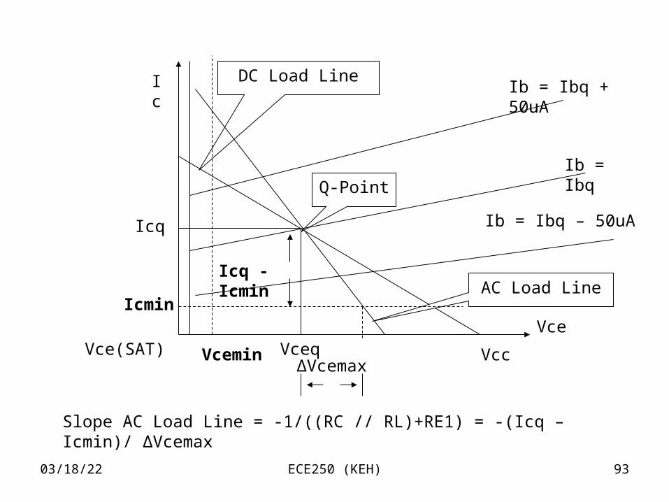
Icmin
Vcemin
Icq - Icmin
Slope AC Load Line = -1/((RC // RL)+RE1) = -(Icq – Icmin)/ ΔVcemax
Ib = Ibq – 50uA
04/18/23 ECE250 (KEH) 94
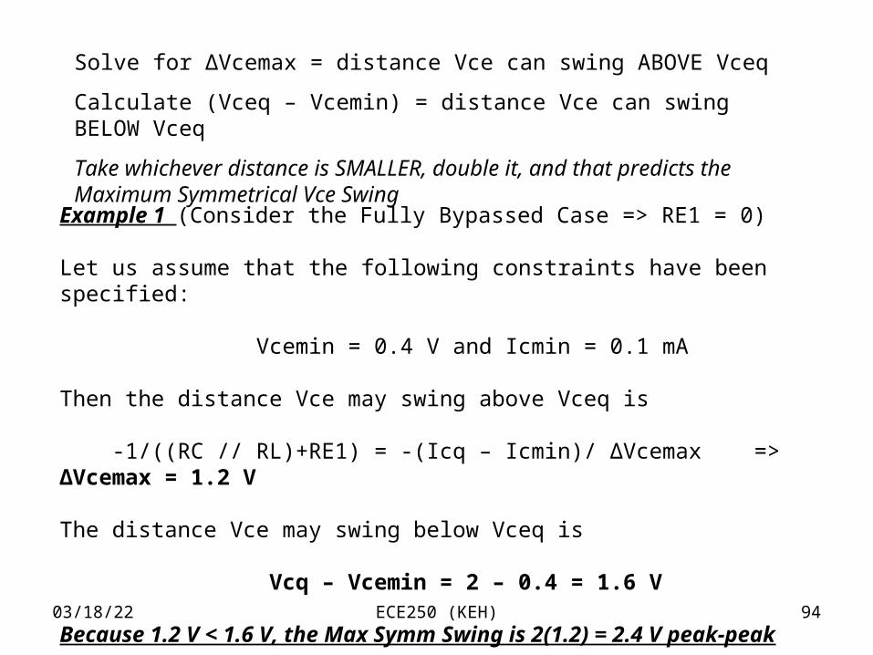
Solve for ΔVcemax = distance Vce can swing ABOVE Vceq
Calculate (Vceq – Vcemin) = distance Vce can swing BELOW Vceq
Take whichever distance is SMALLER, double it, and that predicts the Maximum Symmetrical Vce Swing
Example 1 (Consider the Fully Bypassed Case => RE1 = 0)
Let us assume that the following constraints have been specified:
Vcemin = 0.4 V and Icmin = 0.1 mA
Then the distance Vce may swing above Vceq is
-1/((RC // RL)+RE1) = -(Icq – Icmin)/ ΔVcemax => ΔVcemax = 1.2 V The distance Vce may swing below Vceq is
Vcq – Vcemin = 2 – 0.4 = 1.6 V
Because 1.2 V < 1.6 V, the Max Symm Swing is 2(1.2) = 2.4 V peak-peak
04/18/23 ECE250 (KEH) 95
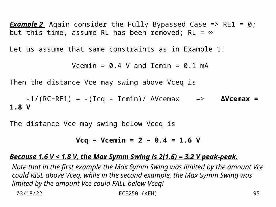
Example 2 Again consider the Fully Bypassed Case => RE1 = 0; but this time, assume RL has been removed; RL = ∞
Let us assume that same constraints as in Example 1:
Vcemin = 0.4 V and Icmin = 0.1 mA
Then the distance Vce may swing above Vceq is
-1/(RC+RE1) = -(Icq – Icmin)/ ΔVcemax => ΔVcemax = 1.8 V The distance Vce may swing below Vceq is
Vcq – Vcemin = 2 – 0.4 = 1.6 V
Because 1.6 V < 1.8 V, the Max Symm Swing is 2(1.6) = 3.2 V peak-peak.
Note that in the first example the Max Symm Swing was limited by the amount Vce could RISE above Vceq, while in the second example, the Max Symm Swing was limited by the amount Vce could FALL below Vceq!
04/18/23 ECE250 (KEH) 96
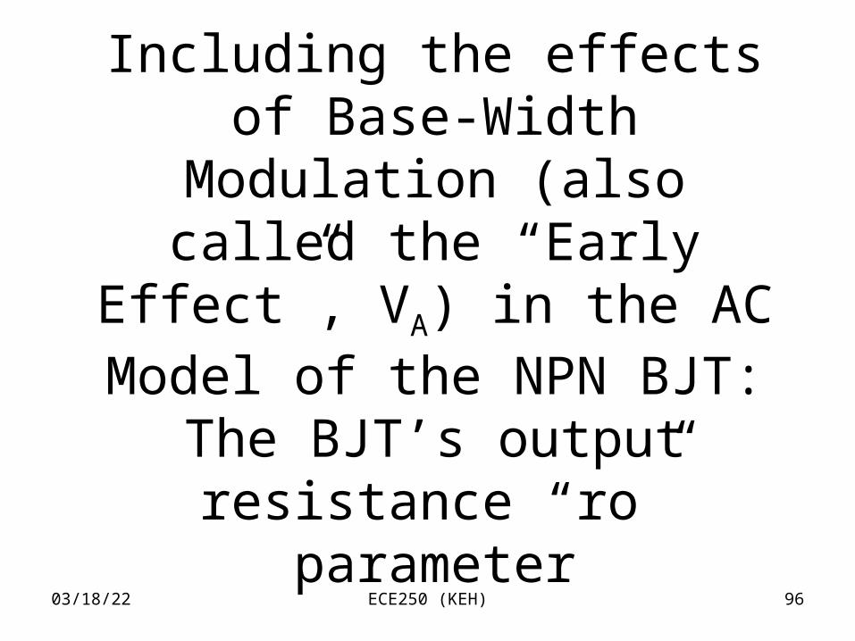
Including the effects of Base-Width Modulation (also called the “Early Effect”, VA) in the AC Model of the NPN BJT: The BJT’s output resistance
“ro” parameter
04/18/23 ECE250 (KEH) 97
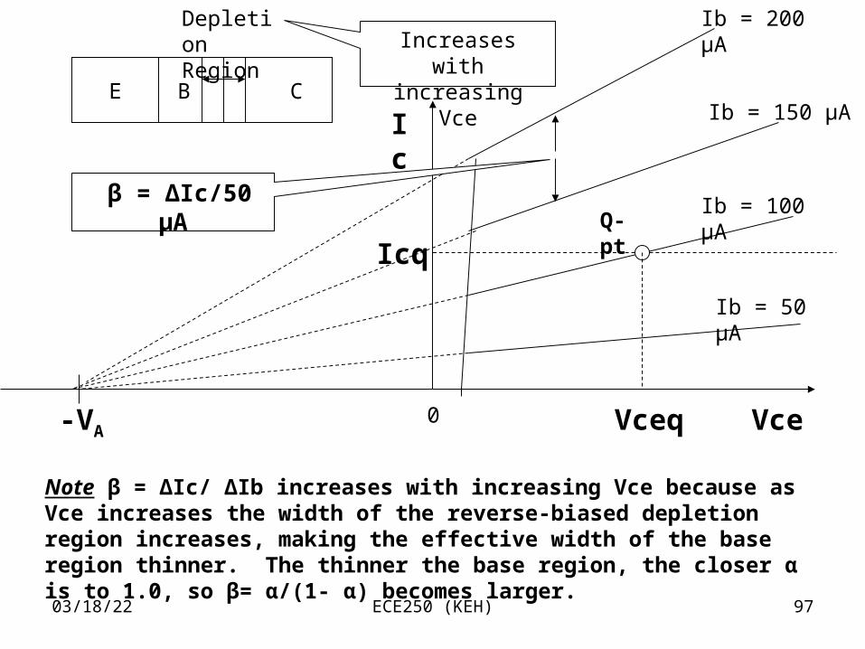
-VA
Ic
Vce0
Q-pt
Icq
Vceq
Ib = 100 μA
Ib = 50 μA
Ib = 150 μA
β = ΔIc/50 μA
Ib = 200 μA
Note β = ΔIc/ ΔIb increases with increasing Vce because as Vce increases the width of the reverse-biased depletion region increases, making the effective width of the base region thinner. The thinner the base region, the closer α is to 1.0, so β= α/(1- α) becomes larger.
E B C
Depletion Region Increases with
increasing Vce
04/18/23 ECE250 (KEH) 98
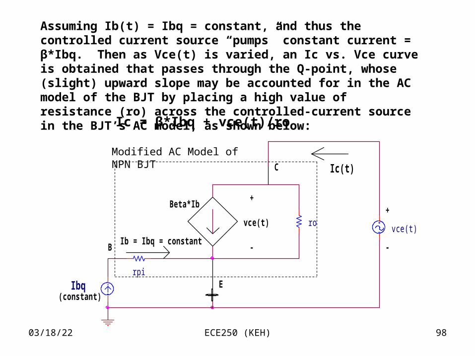
Assuming Ib(t) = Ibq = constant, and thus the controlled current source “pumps” constant current = β*Ibq. Then as Vce(t) is varied, an Ic vs. Vce curve is obtained that passes through the Q-point, whose (slight) upward slope may be accounted for in the AC model of the BJT by placing a high value of resistance (ro) across the controlled-current source in the BJT’s AC model, as shown below:
+
C Ic(t)
-
vce(t)rovce(t)
rpi
Beta*Ib+
E
Ib = Ibq = constant
Ibq
-
(constant)
B
Modified AC Model of NPN BJT
Ic = β*Ibq + vce(t)/ro
04/18/23 ECE250 (KEH) 99
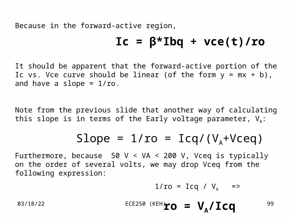
Because in the forward-active region,
Ic = β*Ibq + vce(t)/ro
It should be apparent that the forward-active portion of the Ic vs. Vce curve should be linear (of the form y = mx + b), and have a slope = 1/ro.
Note from the previous slide that another way of calculating this slope is in terms of the Early voltage parameter, VA:
Slope = 1/ro = Icq/(VA+Vceq)
Furthermore, because 50 V < VA < 200 V, Vceq is typically on the order of several volts, we may drop Vceq from the following expression:
1/ro = Icq / VA =>
ro = VA/Icq
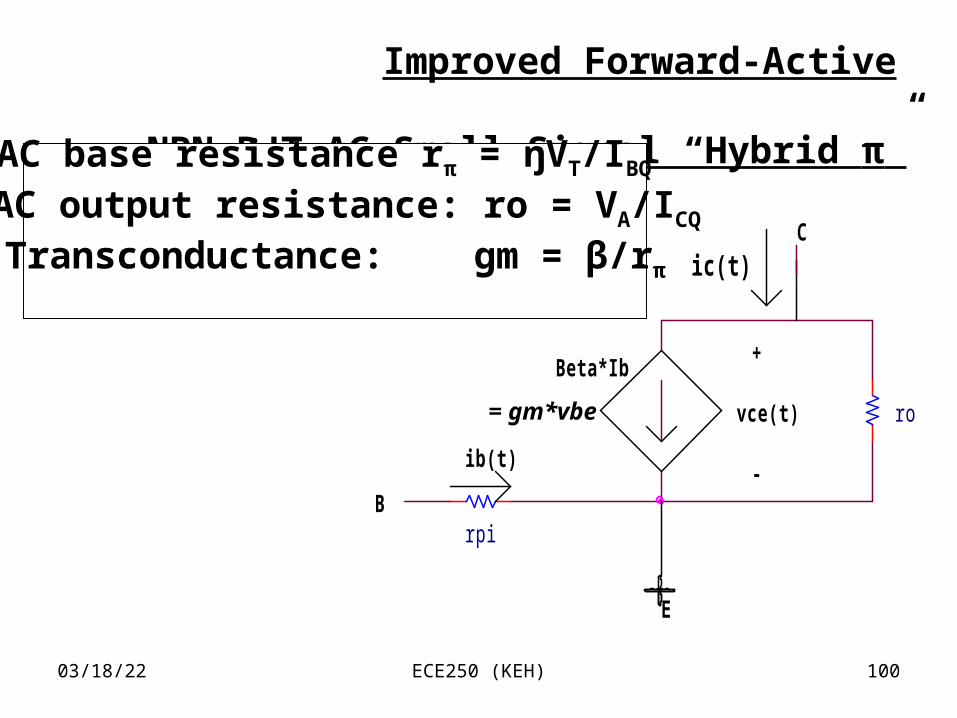
04/18/23 ECE250 (KEH) 100
ib(t)
E
-
ic(t)
+Beta*Ib
C
vce(t)
Brpi
ro
Improved Forward-Active NPN BJT AC Small-Signal “Hybrid π” Model
= gm*vbe
AC base resistance rπ = ŋVT/IBQ AC output resistance: ro = VA/ICQ
Transconductance: gm = β/rπ
04/18/23 ECE250 (KEH) 101
E
ib(t)
Beta*Ib
rpi
ic(t)
ro
C
B
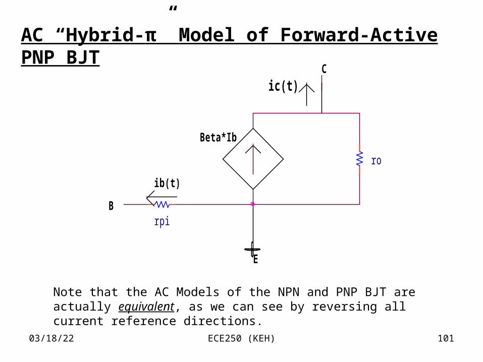
AC “Hybrid-π” Model of Forward-Active PNP BJT
Note that the AC Models of the NPN and PNP BJT are actually equivalent, as we can see by reversing all current reference directions.
04/18/23 ECE250 (KEH) 102
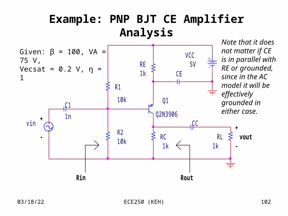
Example: PNP BJT CE Amplifier Analysis
-RL
1k
CC
R1
10k
RE1k
C1
1n
RC1k
Q1
Q2N3906
VCC5V
+
Rout
vin+
vout-
CE
Rin
R210k
Given: β = 100, VA = 75 V,Vecsat = 0.2 V, ŋ = 1
Note that it does not matter if CE is in parallel with RE or grounded, since in the AC model it will be effectively grounded in either case.
04/18/23 ECE250 (KEH) 103
RE1k
VCC5V
R210k
IE
ICRC1k
IBR1
10k Q1
Q2N3906
RC1k
Rth5k
RE1k
VCC5V
Q1
Q2N3906Vth
2.5V
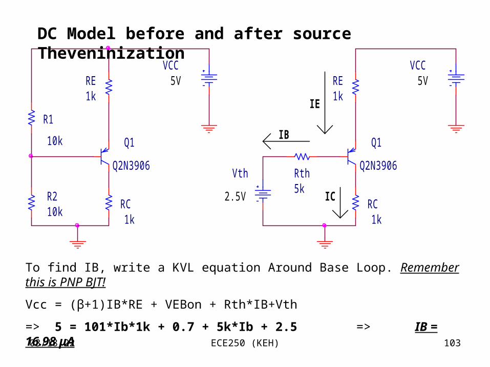
DC Model before and after source Theveninization
To find IB, write a KVL equation Around Base Loop. Remember this is PNP BJT!
Vcc = (β+1)IB*RE + VEBon + Rth*IB+Vth
=> 5 = 101*Ib*1k + 0.7 + 5k*Ib + 2.5 => IB = 16.98 μA
04/18/23 ECE250 (KEH) 104
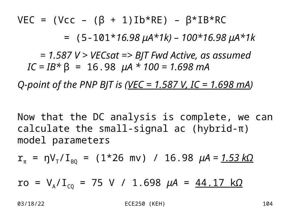
VEC = (Vcc – (β + 1)Ib*RE) – β*IB*RC
= (5-101*16.98 μA*1k) – 100*16.98 μA*1k
= 1.587 V > VECsat => BJT Fwd Active, as assumed IC = IB* β = 16.98 μA * 100 = 1.698 mA
Q-point of the PNP BJT is (VEC = 1.587 V, IC = 1.698 mA)
Now that the DC analysis is complete, we can calculate the small-signal ac (hybrid-π) model parameters
rπ = ŋVT/IBQ = (1*26 mv) / 16.98 μA = 1.53 kΩ
ro = VA/ICQ = 75 V / 1.698 μA = 44.17 kΩ
04/18/23 ECE250 (KEH) 105
RC
1k
Eo
RL
1kR2
10k
oR1
10k o
CBB
o
ro
rpi
Beta*Ib
vin
Co
44.17k
o
1.53k
ic(t)
ib(t)
CE
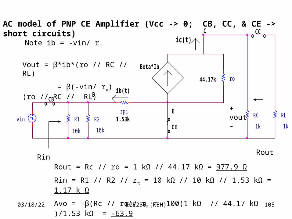
CCAC model of PNP CE Amplifier (Vcc -> 0; CB, CC, & CE -> short circuits)
RinRout
Rout = Rc // ro = 1 kΩ // 44.17 kΩ = 977.9 Ω
Rin = R1 // R2 // rπ = 10 kΩ // 10 kΩ // 1.53 kΩ = 1.17 k Ω
Avo = -β(Rc // ro)/ rπ = -100(1 kΩ // 44.17 kΩ )/1.53 kΩ = -63.9
Note ib = -vin/ rπ
Vout = β*ib*(ro // RC // RL)
= β(-vin/ rπ)(ro // RC // RL)
+vout-
04/18/23 ECE250 (KEH) 106
+
Rout
General Voltage Amp Model
o
-
vout(t)+
RLRin
+vs(t)
-
o
o
RS
--
Load
Avo*vin
Source or Transducer
+
vin(t)
o
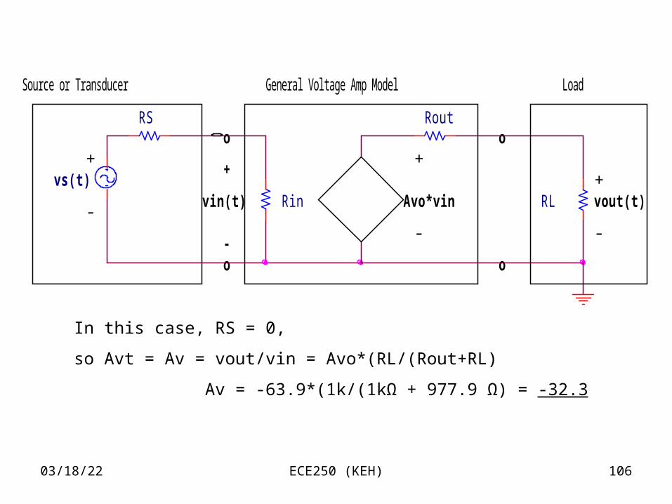
In this case, RS = 0,
so Avt = Av = vout/vin = Avo*(RL/(Rout+RL)
Av = -63.9*(1k/(1kΩ + 977.9 Ω) = -32.3
04/18/23 ECE250 (KEH) 107
Common-Collector (also called Emitter Follower) BJT
Amplifier
Same 3-resistor biasing network and DC model as before, but now the
output is taken across the (unbypassed) emitter resistor, so the
AC model changes dramatically.
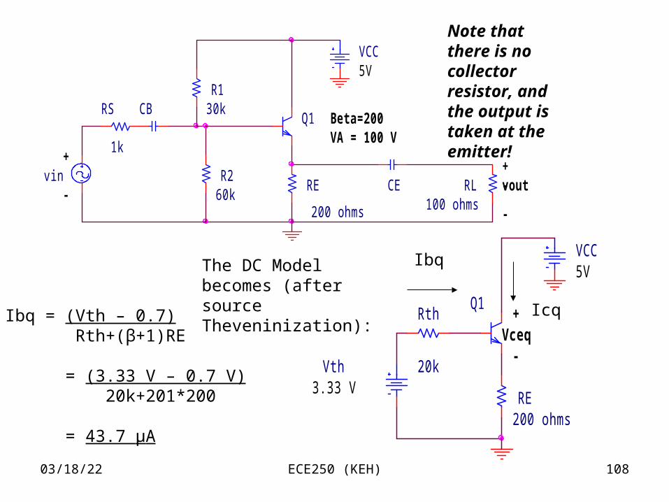
04/18/23 ECE250 (KEH) 108
Note that there is no collector resistor, and the output is taken at the emitter!
+
VCC5V
Q1
RE200 ohms
Vceq
Vth3.33 V
Rth
20k-
The DC Model becomes (after source Theveninization):
Ibq
IcqIbq = (Vth – 0.7) Rth+(β+1)RE = (3.33 V – 0.7 V) 20k+201*200 = 43.7 μA
VA = 100 V
-R2
60k
Beta=200
R130k
voutvin
RS
1k
VCC5V
CERE
200 ohms
CB
+-
+
RL100 ohms
Q1
-
-
04/18/23 ECE250 (KEH) 109
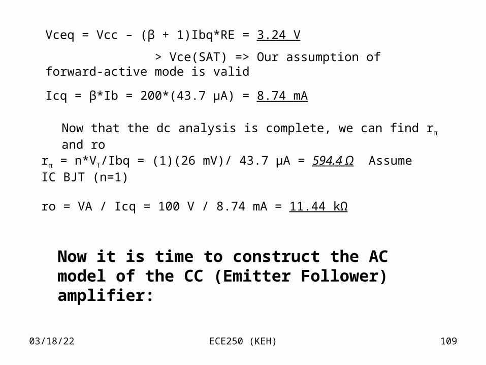
Vceq = Vcc – (β + 1)Ibq*RE = 3.24 V
> Vce(SAT) => Our assumption of forward-active mode is valid
Now that the dc analysis is complete, we can find rπ and ro
Icq = β*Ib = 200*(43.7 μA) = 8.74 mA
rπ = n*VT/Ibq = (1)(26 mV)/ 43.7 μA = 594.4 Ω Assume IC BJT (n=1)
ro = VA / Icq = 100 V / 8.74 mA = 11.44 kΩ
Now it is time to construct the AC model of the CC (Emitter Follower) amplifier:
04/18/23 ECE250 (KEH) 110
E
RE
200 ohms
+
+
vin
vce(t)
R1
30k
Beta*ib
-
-
RS
1k
RL100 ohm
ro
+vs
C
-vout
rpi
-ib
R2
60k
B
+Note that RE, RL, and ro are electrically “in parallel”
AC Model of CC (Emitter Follower) Amplifier
o
o
Rin
o
o
Rout
iin
=594 Ω
=11.4k
Rbin
04/18/23 ECE250 (KEH) 111
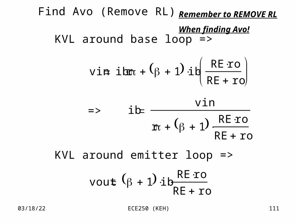
Find Avo (Remove RL)
KVL around base loop =>
vin ib r 1 ibRE ro
RE ro
=> ibvin
r 1 RE roRE ro
KVL around emitter loop =>
vout 1 ibRE ro
RE ro
Remember to REMOVE RL
When finding Avo!
04/18/23 ECE250 (KEH) 112
vout 1 ibRE ro
RE ro
vout 1 vin
r 1 REro
RE ro( )
REro
RE ro( )
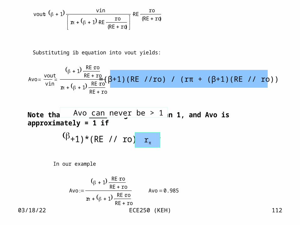
Substituting ib equation into vout yields:
Avovout
vin
1 RE roRE ro
r 1 RE roRE ro
= (+1)*(RE // ro) / (r +1)*(RE // ro))
Note that Avo can never be greater than 1, and Avo is approximately = 1 if
+1)*(RE // ro) >> r
In our example
Avo
1 RE roRE ro
r 1 RE roRE ro
Avo 0.985
rπ
=(β+1)(RE //ro) / (rπ + (β+1)(RE // ro))
Avo can never be > 1
04/18/23 ECE250 (KEH) 113
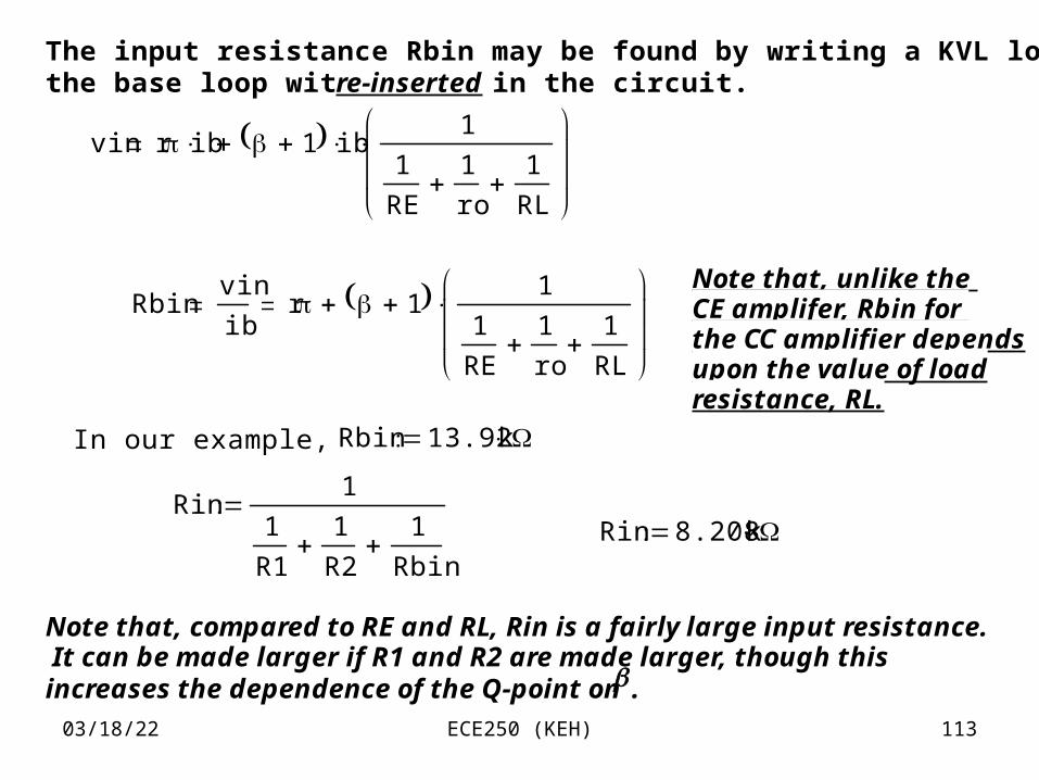
The input resistance Rbin may be found by writing a KVL loop around the base loop with RL re-inserted in the circuit.
vin r ib 1 ib1
1
RE
1
ro
1
RL
Note that, unlike the CE amplifer, Rbin for the CC amplifier dependsupon the value of loadresistance, RL.
Rbinvin
ibr 1 1
1
RE
1
ro
1
RL
In our example, Rbin 13.92 k
Rin1
1
R1
1
R2
1
Rbin
Rin 8.208 k
Note that, compared to RE and RL, Rin is a fairly large input resistance. It can be made larger if R1 and R2 are made larger, though this increases the dependence of the Q-point on .
04/18/23 ECE250 (KEH) 114
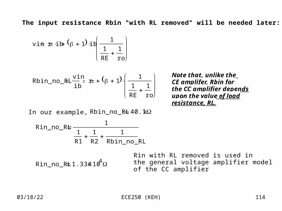
Avo
1 RE roRE ro
r 1 RE roRE ro
The input resistance Rbin "with RL removed" will be needed later:
vin r ib 1 ib1
1
RE
1
ro
Note that, unlike the CE amplifer, Rbin for the CC amplifier dependsupon the value of loadresistance, RL.
Rbin_no_RLvin
ibr 1 1
1
RE
1
ro
In our example, Rbin_no_RL 40.1 k
Rin_no_RL1
1
R1
1
R2
1
Rbin_no_RL
Rin with RL removed is used inthe general voltage amplifier modelof the CC amplifier
Rin_no_RL 1.334 104
04/18/23 ECE250 (KEH) 115
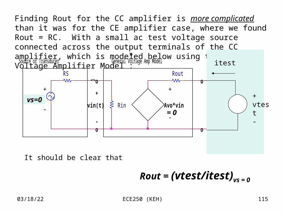
Finding Rout for the CC amplifier is more complicated than it was for the CE amplifier case, where we found Rout = RC. With a small ac test voltage source connected across the output terminals of the CC amplifier, which is modeled below using the “General Voltage Amplifier Model”:
+
Rout
General Voltage Amp Model
o
-
vout(t)+
RLRin
+vs(t)
-
o
o
RS
--
Load
Avo*vin
Source or Transducer
+
vin(t)
o
+vtest-
itest
vs=0
= 0
It should be clear that
Rout = (vtest/itest)vs = 0
04/18/23 ECE250 (KEH) 116
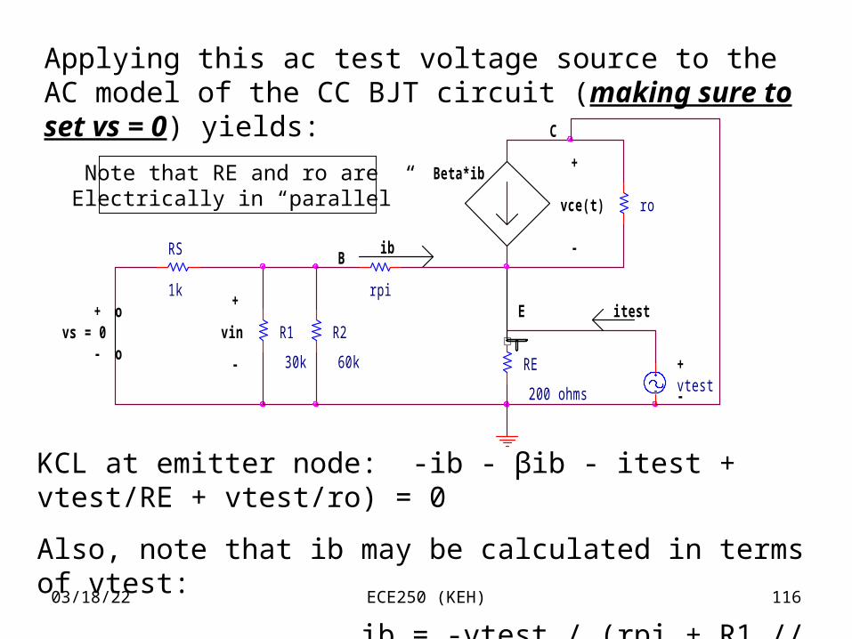
Applying this ac test voltage source to the AC model of the CC BJT circuit (making sure to set vs = 0) yields:
+
Erpi
+
-
rovce(t)
-
itestvs = 0
ib
-
+
-RE
200 ohms
B
Beta*ib
oR2
60kvtest
o
C
vin
RS
1k
R1
30k +
KCL at emitter node: -ib - βib - itest + vtest/RE + vtest/ro) = 0
Also, note that ib may be calculated in terms of vtest:
ib = -vtest / (rpi + R1 // R2 // RS)
Note that RE and ro are Electrically in “parallel”
04/18/23 ECE250 (KEH) 117
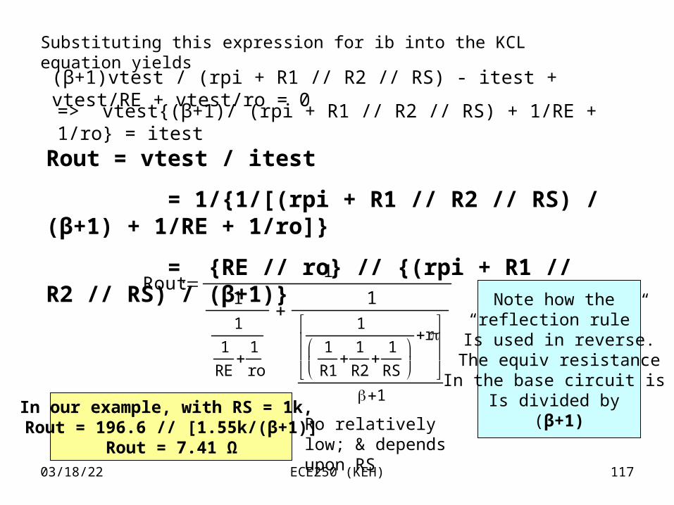
(β+1)vtest / (rpi + R1 // R2 // RS) - itest + vtest/RE + vtest/ro = 0
Substituting this expression for ib into the KCL equation yields
Rout = vtest / itest
= 1/{1/[(rpi + R1 // R2 // RS) / (β+1) + 1/RE + 1/ro]}
= {RE // ro} // {(rpi + R1 // R2 // RS) / (β+1)}
=> vtest{(β+1)/ (rpi + R1 // R2 // RS) + 1/RE + 1/ro} = itest
Rout1
11
1
RE
1
ro
11
1
R1
1
R2
1
RS
r
1
Rout 30.516
Note how the “reflection rule”
Is used in reverse.The equiv resistanceIn the base circuit is
Is divided by (β+1)
In our example, with RS = 1k, Rout = 196.6 // [1.55k/(β+1)]
Rout = 7.41 Ω
Ro relatively low; & depends upon RS
04/18/23 ECE250 (KEH) 118
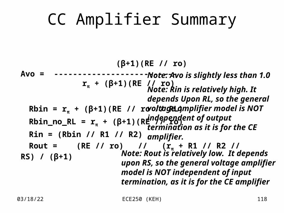
CC Amplifier Summary
(β+1)(RE // ro)Avo = -------------------------- rπ + (β+1)(RE // ro)
Rbin = rπ + (β+1)(RE // ro // RL)
Rbin_no_RL = rπ + (β+1)(RE // ro)
Rin = (Rbin // R1 // R2)
Rout = (RE // ro) // (rπ + R1 // R2 // RS) / (β+1)
Note: Avo is slightly less than 1.0
Note: Rin is relatively high. It depends Upon RL, so the general voltage amplifier model is NOT independent of output termination as it is for the CE amplifier.
Note: Rout is relatively low. It depends upon RS, so the general voltage amplifier model is NOT independent of input termination, as it is for the CE amplifier
04/18/23 ECE250 (KEH) 119
But what good is the CC (Emitter Follower) Amplifier, since it has a voltage gain
that is slightly less than unity? What advantage does this
amplifier have over a wire that connects input to output?
04/18/23 ECE250 (KEH) 120
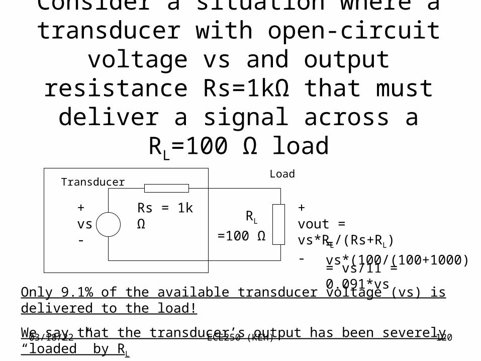
Consider a situation where a transducer with open-circuit voltage vs and output resistance Rs=1kΩ that must deliver a
signal across a RL=100 Ω load
+vs-
Rs = 1k ΩRL
+vout = vs*RL/(Rs+RL)-=100 Ω
= vs*(100/(100+1000)
= vs/11 = 0.091*vs
Only 9.1% of the available transducer voltage (vs) is delivered to the load!
We say that the transducer’s output has been severely “loaded” by RL
TransducerLoad
04/18/23 ECE250 (KEH) 121
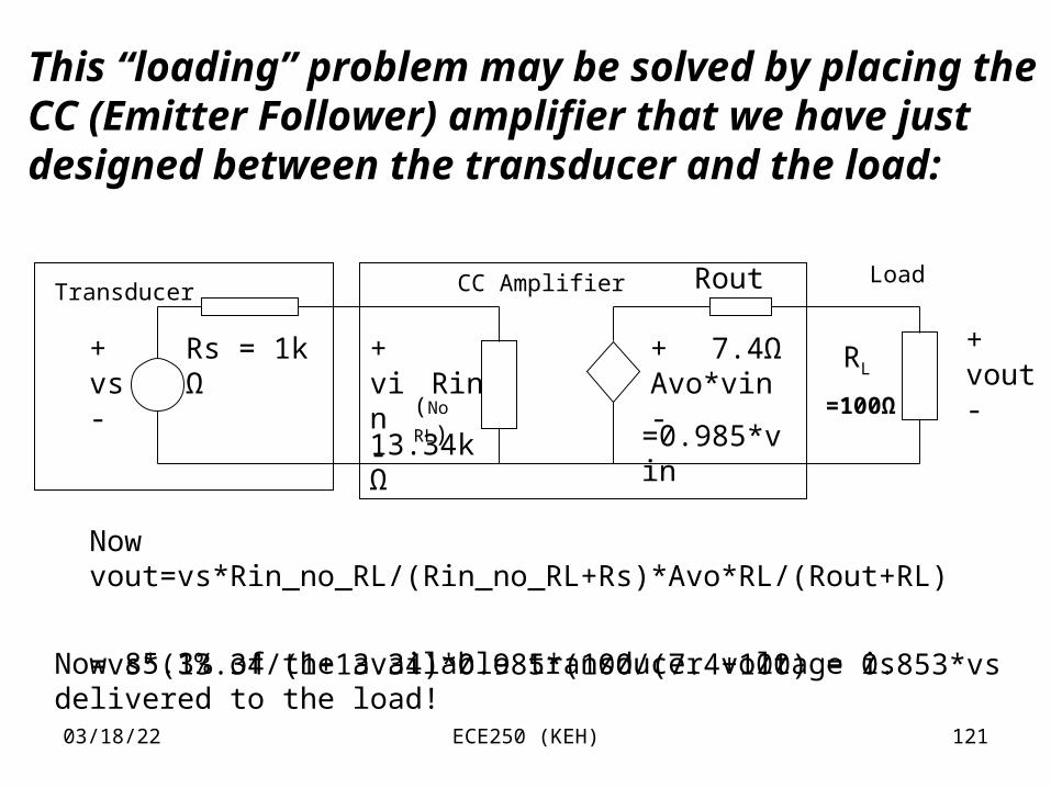
+vs-
Rs = 1k Ω RL
=100Ω
Transducer
Rin
Rout
+Avo*vin-
CC Amplifier Load
This “loading” problem may be solved by placing the CC (Emitter Follower) amplifier that we have just designed between the transducer and the load:
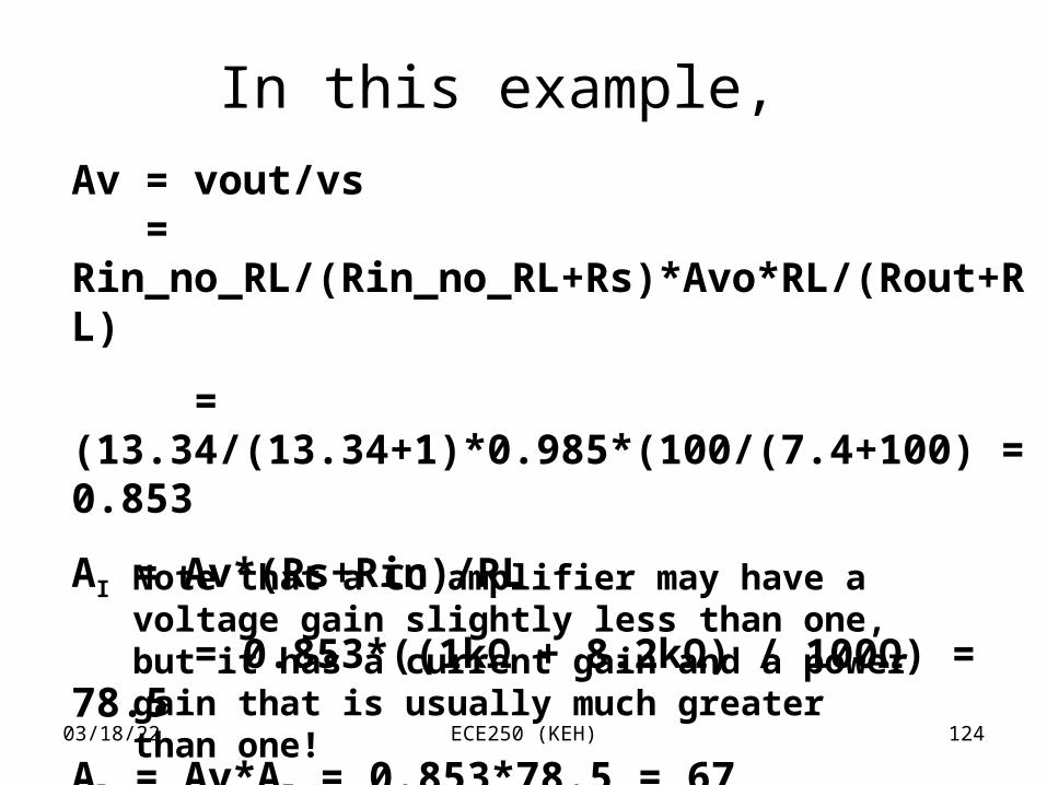
7.4Ω+vin-13.34kΩ =0.985*vin
Now vout=vs*Rin_no_RL/(Rin_no_RL+Rs)*Avo*RL/(Rout+RL)
=vs*(13.34/(1+13.34)*0.985*(100/(7.4+100) = 0.853*vs
+vout-
Now 85.3% of the available transducer voltage is delivered to the load!
(No RL)
04/18/23 ECE250 (KEH) 122
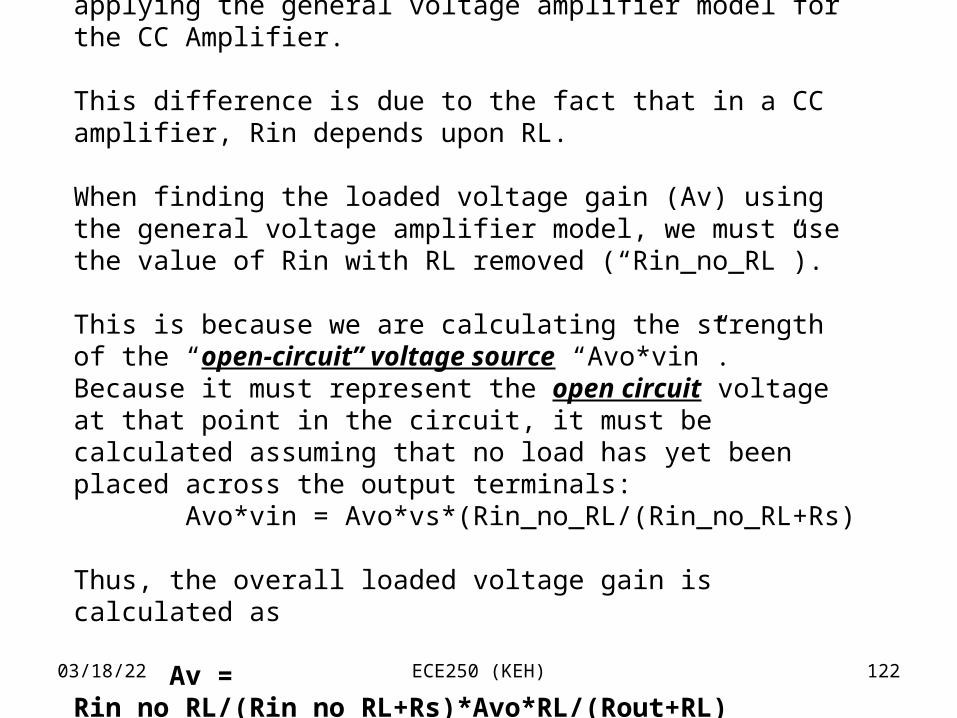
Note that there is a very subtle difference in applying the general voltage amplifier model for the CC Amplifier.
This difference is due to the fact that in a CC amplifier, Rin depends upon RL.
When finding the loaded voltage gain (Av) using the general voltage amplifier model, we must use the value of Rin with RL removed (“Rin_no_RL”).
This is because we are calculating the strength of the “open-circuit” voltage source “Avo*vin”. Because it must represent the open circuit voltage at that point in the circuit, it must be calculated assuming that no load has yet been placed across the output terminals: Avo*vin = Avo*vs*(Rin_no_RL/(Rin_no_RL+Rs)
Thus, the overall loaded voltage gain is calculated as
Av = Rin_no_RL/(Rin_no_RL+Rs)*Avo*RL/(Rout+RL)
04/18/23 ECE250 (KEH) 123
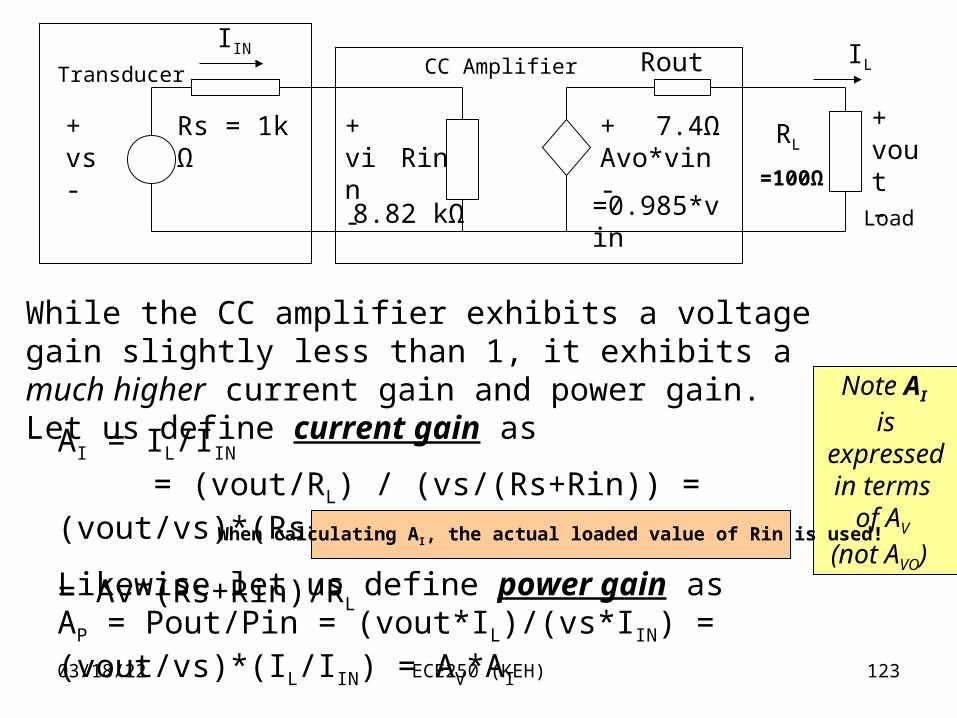
+vs-
Rs = 1k Ω RL
=100Ω
Transducer
Rin
Rout
+Avo*vin-
CC Amplifier
Load
7.4Ω+vin-8.82 kΩ =0.985*vin
IIN IL
+vout-
While the CC amplifier exhibits a voltage gain slightly less than 1, it exhibits a much higher current gain and power gain. Let us define current gain as
AI = IL/IIN = (vout/RL) / (vs/(Rs+Rin)) = (vout/vs)*(Rs+Rin)/RL
= Av*(Rs+Rin)/RL
Note AI
isexpressedin terms
of AV (not AVO)
Likewise let us define power gain asAP = Pout/Pin = (vout*IL)/(vs*IIN) = (vout/vs)*(IL/IIN) = AV*AI
When calculating AI, the actual loaded value of Rin is used!
04/18/23 ECE250 (KEH) 124
In this example,
Av = vout/vs = Rin_no_RL/(Rin_no_RL+Rs)*Avo*RL/(Rout+RL)
= (13.34/(13.34+1)*0.985*(100/(7.4+100) = 0.853
AI = Av*(Rs+Rin)/RL
= 0.853*((1kΩ + 8.2kΩ) / 100Ω) = 78.5
AP = Av*AI = 0.853*78.5 = 67Note that a CC amplifier may have a voltage gain slightly less than one, but it has a current gain and a power gain that is usually much greater than one!

04/18/23 ECE250 (KEH) 125
Finding Maximum Symmetrical Vce Output Swing for CC Amplifier
(Use our present example)
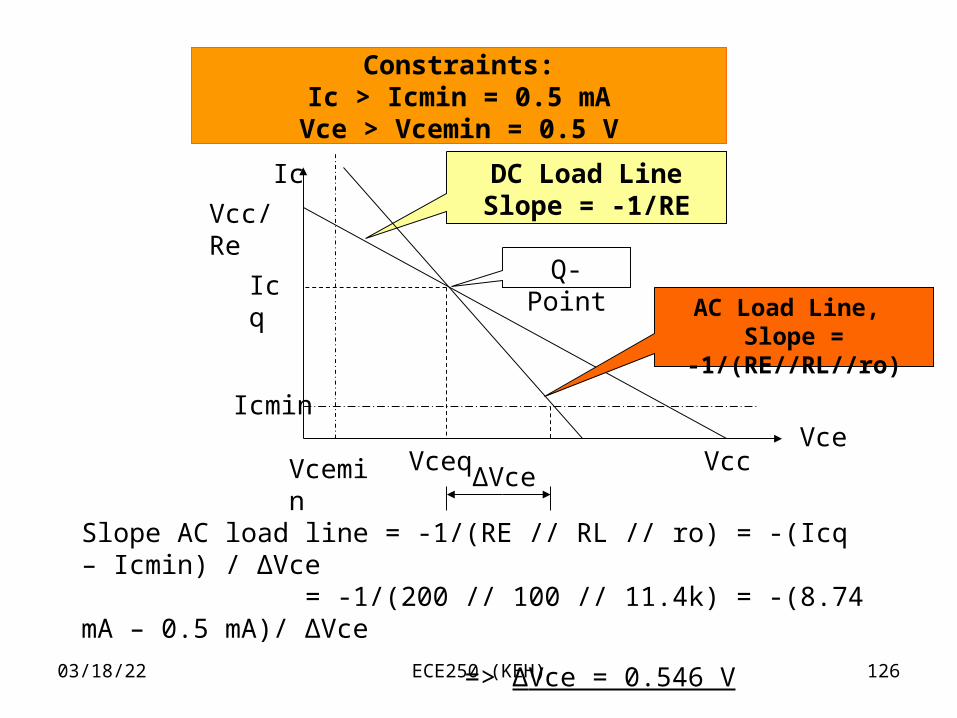
04/18/23 ECE250 (KEH) 126
Constraints:Ic > Icmin = 0.5 mA
Vce > Vcemin = 0.5 V
Ic
VceVcc
Vcc/Re
DC Load LineSlope = -1/RE
AC Load Line, Slope = -1/(RE//RL//ro)
Q-Point
Vceq
Icq
Icmin
Vcemin ΔVce
Slope AC load line = -1/(RE // RL // ro) = -(Icq – Icmin) / ΔVce = -1/(200 // 100 // 11.4k) = -(8.74 mA – 0.5 mA)/ ΔVce
=> ΔVce = 0.546 V
04/18/23 ECE250 (KEH) 127
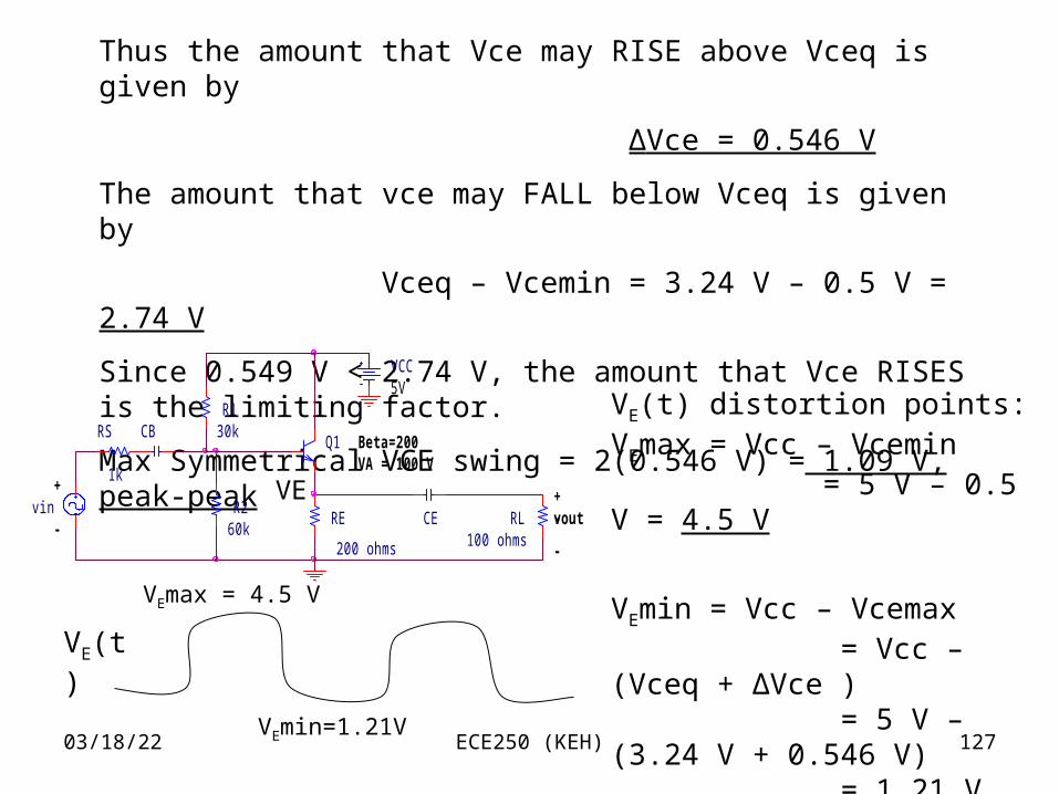
Thus the amount that Vce may RISE above Vceq is given by
ΔVce = 0.546 V
The amount that vce may FALL below Vceq is given by
Vceq – Vcemin = 3.24 V – 0.5 V = 2.74 V
Since 0.549 V < 2.74 V, the amount that Vce RISES is the limiting factor.
Max Symmetrical VCE swing = 2(0.546 V) = 1.09 V, peak-peak
VA = 100 V
-R2
60k
Beta=200
R130k
voutvin
RS
1k
VCC5V
CERE
200 ohms
CB
+-
+
RL100 ohms
Q1
-
-
VE(t) distortion points:VEmax = Vcc – Vcemin = 5 V – 0.5 V = 4.5 V
VEmin = Vcc – Vcemax = Vcc – (Vceq + ΔVce ) = 5 V – (3.24 V + 0.546 V) = 1.21 V
VEmax = 4.5 V
VEmin=1.21V
VE(t)
VE
04/18/23 ECE250 (KEH) 128
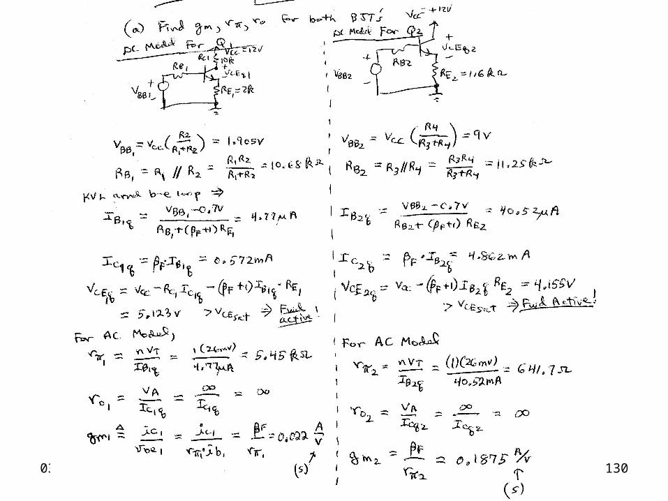
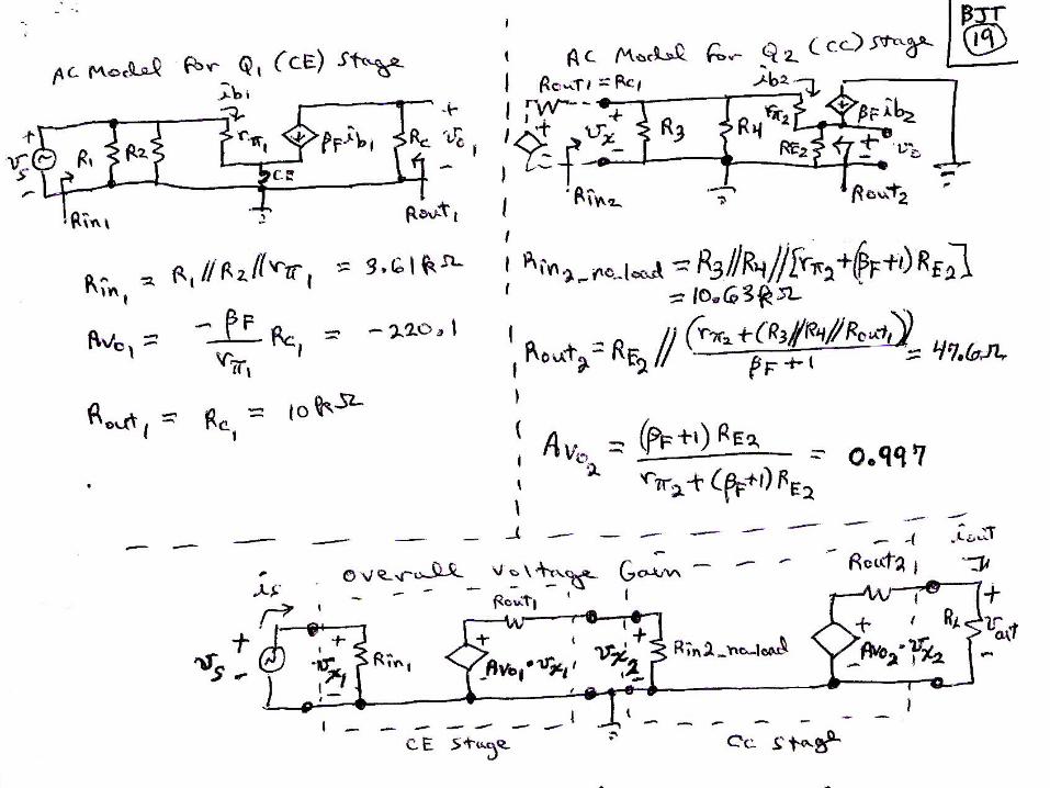
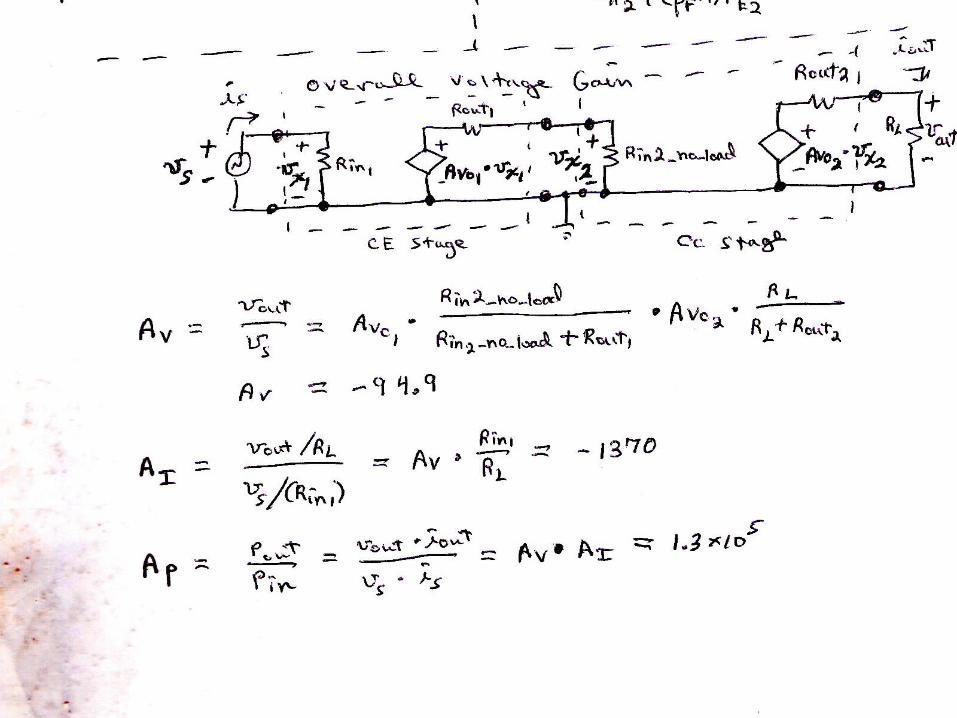
Cascading two amplifier stages using the general voltage amplifier model
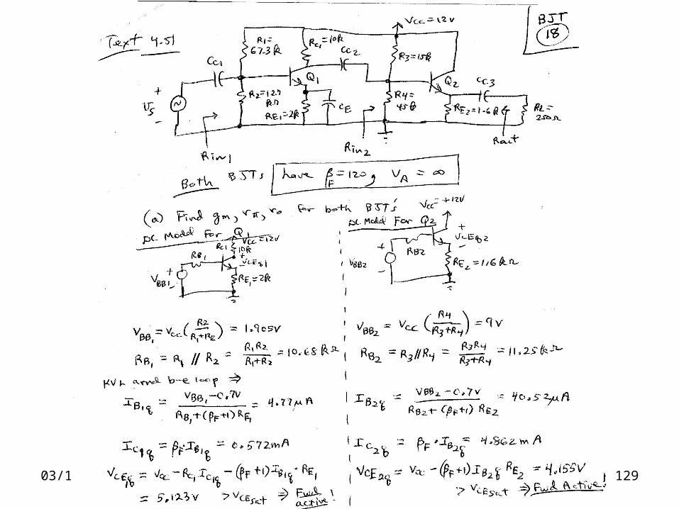
04/18/23 ECE250 (KEH) 129
04/18/23 ECE250 (KEH) 130
04/18/23 ECE250 (KEH) 131
04/18/23 ECE250 (KEH) 132

04/18/23 ECE250 (KEH) 133
THE END OF BJT Coverage!
(MOSFETs come next)


