A Novel Probe Station for Helium Temperature On-Wafer Measurements
H. Geissler1, A.Rumiantsev1, S. Schott1, P. Sakalas2,3 and M. Schroter2,4
1 SUSS MicroTec Test Systems, 01561 Sacka, Germany 2 Dresden University of Technology, CEDIC, 01062 Dresden, Germany
3Semiconductor Physics Institute, Fluctuation Phenomena Lab., 01108 Vilnius, Lithuania 4University of California San Diego, ECE, La Jolla, CA 92093-0407, USA
Abstract — A novel automated wafer-level RF measurement
system is presented. It includes a wafer prober and dedicated on-wafer probe tips and calibration standards. Probe station related design issues are discussed leading to a system for automated testing of wafers up to 300mm by using a programmable positioning stage. Using on-wafer SiGe HBT measurements, noise characterization and VNA calibration verification, the long-term stability and reliability of the setup is illustrated. Tests are carried out both with liquid nitrogen as well as liquid helium as coolant, equal to temperature range from 400K down to 4K.
Index Terms — Automatic test equipment, cryogenics, calibration, microwave measurements, probing, SiGe HBT, RF noise, noise measurement.
I. INTRODUCTION
Cryogenic-temperature measurements are becoming more and more important in different fields of microelectronics. New types of devices such as MEMS, new or growing applications like superconductors and new characterization techniques generate the need for appropriate test equipment. For example, space applications, such as spatial and spectral filtering to accommodate the high density of satellites in geo-stationary orbit, require cryogenic very low noise amplifiers (LNAs) [1]. The design of cooled low noise LNAs is based on accurate compact models (CM) of active and passive circuit elements. For CM parameter extraction, the knowledge of DC, RF, microwave and noise trends of the circuit elements at cryogenic temperatures is of primary importance. This and other space applications like very long wavelength infrared (VLWIR) detectors [2] require probing equipment for deep cryogenic temperatures (T<10K).
Cryogenic probe stations have been developed since the 1980’s. Over time, the systems were improved, and today have reached a status where small samples (e.g. 1”x1”) or even wafers up to 4” can be probed down to T=4.2K (liquid helium temperature). The common technology [3, 4, 5] uses open-loop cooling cycles instead of refrigerators, offering more cooling power and less vibration, but causing consumption of valuable liquid helium (LHe). Systems consist of a small vacuum chamber with the sample holder inside and manipulators with single probes, which are coupled to the chamber by bellows. The manipulation stages
are placed outside the chamber. In order to achieve a reasonable probe movement range, long metal bellows are required to provide movement flexibility. Thus, probing using such setups introduces limitations, caused by the high forces introduced from the bellows and needed probe arm length. Insufficient quality of probe positioning, low stability over time and vibration sensitivity results in unreliable electrical contact with the device under test (DUT).
In this paper we present a new generation of cryogenic probe station, allowing test on wafers up to 300mm with high positioning accuracy, providing reliable long-term electrical contact with the DUT’s and a motorized chuck stage for performing automated test routines.
II. SYSTEM DESCRIPTION
A. Probe station
To overcome issues mentioned in section I, a new design approach has been developed and realized (Fig.1) [6]. A large high vacuum (HV) chamber (leak rate < 1E-09 mbar*l/s) accommodates the X-Y-Z-Θ chuck stage carrying the thermally-isolated cryogenic chuck on top. Tests showed that the stage remains warm (T≥10°C) during cryogenic operation guaranteeing the same positioning performance as under ambient conditions. A HV environment requires use of brushless motors, so stepper motors were chosen for driving the stage. Using glass scale encoder feedback in combination with software compensation algorithms, absolute positioning accuracy is better than +/-5µm and repeatability better than +/-2.5µm.
Cryogenic shielding is essential to prevent background radiation when testing IR detectors or to achieve deep cryogenic temperatures. An opening in the center of the shield provides access for single probes or probecard.
To eliminate the influence of bellows, probe manipulation stages are placed on a warm support inside the chamber. Also probe arm length can be reduced to 10cm, which is shorter compared to common solution. By using high precision stages with 100tpi screws, a movement resolution of 3µm is finally achieved for all three axes. Thus, RF probes with pitch down to 50µm can be placed accurately on the pads. To cool
the probe tips, thermal isolation is integrated in the arms and flexible copper braids connecting to the shield remove heat. To eliminate heat flow from the warm chamber feedthroughs to the DUT, the cables are cooled using the same principle. Thermal drift during cooldown is unavoidable (ΔT≈300K) and makes external manipulation necessary. Commercially available rotary feedthroughs were used.
DewarTemperature control unit
Gas pumps
Heat exchangerCold shield
Super-isolated transfer line
Col
d va
lve
1
Col
d va
lve
2
Fig.2. Cryogenic flow chart of the system
Fig.1. SUSS PAC200/300 semiautomatic cryogenic probe station
0
50
100
150
200
250
300
0 120 240 360 480 600 720Time [min]
Tem
pera
ture
[K]
Chuck Shield /Z/Probe
Fig.3. Temperatures of the chuck, shield and probe over time, using LN2 as a coolant.
B. Cryogenic system
Available refrigerators offer a maximum 1.5W cooling power at 4.2K, whereas an open loop system offers 6 to 10W. This higher power is required to reach deep temperatures with large substrates. Furthermore, open loop systems do not generate vibration and thus noise influencing the measurements. For automated stepping over the whole wafer and to maintain constant contact resistance, high chuck surface flatness (≤15µm) is needed. With a substrate size up to 300mm, the cryogenic chuck size must be dimensioned adequately, resulting in a higher thermal mass for cooling. In order to keep cool-down time at a reasonable level, two independent cooling circuits for both the chuck and shield are preferable. To lower estimated consumption of liquid gas and system costs a different solution has been developed. Coolant flow is redirected by cold valves (Fig.2). The physical mechanism known as cryogenic pump effect [7], where cold surfaces attract gas molecules can be adapted in order to achieve a condensation-free test environment. By cooling down the cryogenic shield first, the cryogenic pump effect will cause residual gas to be trapped at the shield surface and not the chuck or DUT, respectively. The trapping temperature depends on the freezing and boiling points of the latter gases. As mass spectrometer analysis showed that the evacuated chamber mainly contains N2, H2O, O2, but also a wide spectrum of others. An experimental approach was chosen and showed that DUT can be kept free of condensates for Tshield<160K.
0
50
100
150
200
250
300
0 120 240 360 480 600 720
Time [min]
Tem
pera
ture
[K]
Chuck Shield /Z/Probe
Fig. 4. Temperatures of the chuck, shield and probe over time, using LHe as coolant.
For ease of use and fail-safe operation coolant flow control was automated. An algorithm was implemented that used Tchuck and Tshield as inputs. In state 1 during cooldown, the shield is pre-cooled first. In state 2, the system switches to chuck cooldown causing Tshield to rise. If Tshield≥160K, state 1 is enabled again. This procedure remains active until the chuck has reached desired test temperature (state 3). Then the shield is off-gas-cooled, yielding its minimum temperature of
2
~25K as the chuck temperature comes down to 4K. Cooldown tests were carried out with both LN2 (Fig. 3) and LHe (Fig. 4). Temperature can be held stable at the lowest defined value within +/-0.05 K for Tchuck>20K and within +/-0.1K for Tchuck<20K using DC heaters for temperature control. Maximum test time depends on consumption and the available amount of liquid gas. Using 100l dewars, cooldown and operation at the cold temperature for more than 6 hours was demonstrated. With liquid helium, a minimum temperature of 4.03K was achieved with a 200mm wafer.
III. RF ACCESSORIES
Under laboratory test conditions and at ambient temperatures, it is well known that thermal variation of the RF accessories is a source of non-systematic error, which reduces measurement accuracy. There is no difference under cryogenic test conditions. All test accessories within the controlled environment must be impervious to extreme cold and vacuum conditions and exhibit stable thermal behavior. Cryogenic temperatures cause mechanical and electrical changes in all RF components. However, when stable cryogenic temperatures are established, the electrical changes in the setup can be corrected with a planar calibration. Therefore, calibration must occur at the same stable temperature as the tests.
A. Cryogenic Wafer Probe Tips
The probe station keeps the RF cable and wafer probes stable in the mounting conditions. There is no relative movement in the cooling area of any parts, with exception of the probe’s contact springs. Movement is confined to the portion of the cable that remains flexible outside the super-cooled environment.
The RF wafer probes used, the Cryogenic |Z| Probe, are designed with total air isolation, which is absolutely necessary for such tests. In the cryogenic test environment, special materials are in use, such as cryogenically-tested plastics. Additionally, nickel is used as material for the coplanar waveguide (CPW) and stays flexible when in contact with the DUT. It exhibits low contact resistance at all temperatures, including those in the cryogenic range.
The probe tips need to be cooled to a temperature close to that of the DUT, eliminating any unwanted temperature influences of the probe tips on the results. To reduce the mass which must be cooled, the cryogenic probe is designed with a small case. Using this set-up, a temperature difference lower than 30K between the DUT and the probe contacts was achieved (Fig. 3, 4).
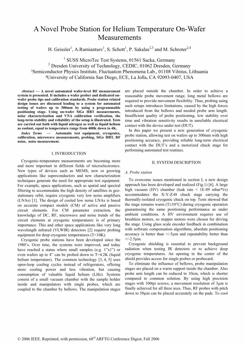
B. RF Cables
The first 10cm of the 50GHz cables leading from the |Z| Probes are also included in the cooling system (Fig. 5). At these temperatures, the cables become very brittle, and any movement can cause the cable to be damaged or break.
Therefore, this part of the cable is mechanically included into the manipulator, which ensures no relative movement between the cable and the probe. The rest of the cable is not subject to the cold temperatures and can move together with the X-Y-Z stage of the manipulator (10mm in each direction). The total cable length in the chamber is approximately 40cm.
Fig. 5. Cryogenic accessories
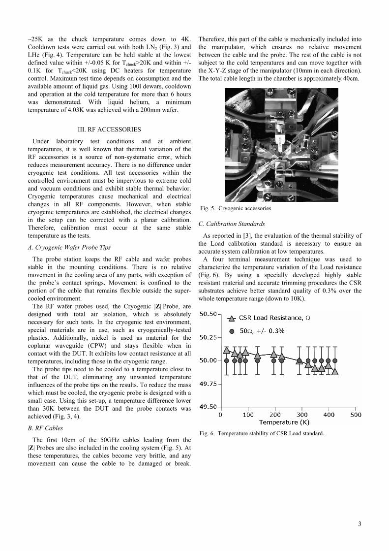
C. Calibration Standards
As reported in [3], the evaluation of the thermal stability of the Load calibration standard is necessary to ensure an accurate system calibration at low temperatures.
A four terminal measurement technique was used to characterize the temperature variation of the Load resistance (Fig. 6). By using a specially developed highly stable resistant material and accurate trimming procedures the CSR substrates achieve better standard quality of 0.3% over the whole temperature range (down to 10K).
Fig. 6. Temperature stability of CSR Load standard.
3
IV. CRYOGENIC CALIBRATION
A. Accuracy and Dynamic Range
In contrast to a conventional wafer level measurement system, accurate calibration of the cryogenic setup raises new challenges. The electrical characteristics of calibration standards demonstrate a significant dependence on temperature, which drastically reduces the accuracy of the calibration at cryogenic temperatures.
Another important property of the wafer-level RF and microwave setup is the calibration dynamic range. This parameter is typically proportional to the inverse of the measurement frequency. That is, a larger value of the calibration dynamic range provides more accurate measurement results. Additionally, a system providing good calibration dynamic over all frequencies of interest can be configured for significantly faster measurements without an impact on the accuracy of measurement results (e.g. increasing the IFBW value – the intermediate frequency filter bandwidth of the vector network analyzer (VNA) receivers or decreasing the average factor). Therefore, an expensive cooling medium, such as LHe, can be saved and the number of the experiments within one cooling circle can be increased.
The simple way to evaluate the calibration dynamic range is provided by measurement of a well-matched element (e.g. the Thru standard). For the experimental evaluation of the cryogenic system’s calibration accuracy and dynamic range, an Agilent 50GHz PNA E8364B was used. The VNA IFBW value was set to 100Hz and the averaging was switched off. The system was calibrated with the help of the LRM+ technique using the Thru, Short, and Load standards on the CSR-3 calibration substrate at different temperatures.
Another Thru element from the CSR-3 was used as the verification element and its insertion loss S21 and return loss S11 were measured. Fig. 7 demonstrates the results at room temperature and 4K.
The calibration dynamic range is better than 49dB up to 50GHz for both temperature cases. The insertion loss varies negligibly from its ideal value of 0dB. The room temperature and 4K results demonstrate excellent agreement, except for the variation in the return loss value up to 5GHz. Obviously, this difference is caused by the Load resistance temperature variation, which was not considered in this experiment. However, the results at 4K are common for room temperature measurement set-ups and acceptable for most measurement applications. If further accuracy improvement is necessary, the temperature influence on the Load resistance can be easily taken into account, as described in [9].
B. Calibration Stability
The measurement system was reconfigured for the further measurements using a 40GHz Agilent 8722ES VNA opt. 400. The stability of the whole system at room temperature and 4K during the experimental time was calculated with the help of the procedure recommended in [10] and the MultiCal® software package*. Additionally, the accuracy of the used LRM+ calibration was verified using the calibration comparison technique [11].
Since the recommended reference material RM8130* for the calibration verification is not specified at cryogenic temperatures, the reference multiline TRL calibration [12] was done on the same alumina substrate. The characteristic impedance of the alumina lines was extracted using the method from [13] and verified for use for commercially available alumina coplanar wave guide lines (CPW) [14].
The obtained results (Fig. 8) prove that the drift of the measurement setup at cryogenic temperatures is comparable to the drift of the measurement system at room temperature.
Fig. 8. Verification of the measurement system drifts at the room temperature and at the 4K within the experimental time, as well as the measurement accuracy of the 4K LRM+ calibration. Data are presented for the system configured with the Agilent 8722ES VNA, opt. 400.
Fig. 7. Verification of accuracy and dynamic range of the LRM+ calibration at room temperature (RT) and 4K using the Thru element. The slight variation in the return loss is caused by temperature changes of the Load resistance of 0.3%, not considered in this experiment.
* Available from the National Institute of Standards and Technology, USA
4
Additionally, it was demonstrated that the calibration accuracy at the lowest temperature of 4K is comparable with the accuracy reported for a conventional setup [8, 14].
J C,Jb[mA{µm2}]
VBE[V]
1e-007
1e-006
1e-005
0.0001
0.001
0.01
0.1
1
10
0.4 0.6 0.8 1 1.2 1.4
4K 70K 300K
J C,Jb[mA{µm2}]
VBE[V]
1e-007
1e-006
1e-005
0.0001
0.001
0.01
0.1
1
10
0.4 0.6 0.8 1 1.2 1.4
4K 70K 300K
Fig.10. Forward Gummel plot of SiGe HBT with CBEB configuration and emitter area of: AE0=0.5*20.3 µm2. VCE=1.5V.
V. DC, RF AND HF NOISE BEHAVIOR OF SIGE HBT AT 300K, 70K AND 4K
DC, RF and high frequency noise measurements have been carried out on SiGe HBTs, located on a 200 mm wafer [15, 16]. LEC (Low Emitter Concentration) HBTs, features current gain cut-off frequency fT=90 GHz at T0=300K. Measured devices have CBE and CBEB configuration with emitter areas of AE0=0.3*20.3 µm2 and 0.5*20.3 µm2
respectively. The transistor biasing was set using 50GHz HP11612B Kelvin bias tees and GPIB controlled semiconductor parameter analyzer HP4142. Scattering parameters (SXX, SXY) were measured with Agilent 8722ES opt. 400 VNA in f[GHz]=0.1, 40 frequency range. I(V) characteristics and RF response were measured using IC-CAP standard n-p-n transistor measurement master file. VNA calibration was verified by in-house (SUSS MicroTec) routines as well as using IC-CAP calibration verification method [17]. Transistors were embedded on GSG pads with 150µm pitch. An impact of the pad parasitics was removed using two step (“open” and “short” dummies) de-embedding procedure. Note that equivalent circuit parameters of the “dummies” did change against the temperature. Therefore each T required a separate measurement of dummy structures. Pad de-embedding was verified using transmission line concept and exploiting on-wafer “thru” structure: the “point” of SXX, obtained at 50Ω in the Smith chart and for magnitude of SXY=1 in polar plot after de-embedding of an “open” and “short” from the “thru” was an indication of correct de-embedding. High frequency noise factor ((NF50) in 50Ω system) was measured using spectrum analyzer Agilent E4440A set in a noise figure measurement mode. Calibration of the noise system was performed using “thru” structure on calibration substrate in the cooled chamber of the probe station.
SiGe HBT at T=70K and 4K exhibited fair performance (Fig. 9-13). A set-on VBE for 4K case is shifted towards higher VBE in comparison to T=300K. Base current (IB) is reduced due to the partial freeze out of impurities in the base. Note that bumps on the I
B
BB (Fig. 10), which are better expressed in the forward Gummel plot for larger emitter area device AE0=0.5*20.3 µm2 are repeatable in time domain and statistically and might be associated with the tunneling current domination instead of diffusion. Despite reduced IB, collector current (I
B
C) remains fairly high, so yielding extremely high DC current gain (Fig. 11).
BF
0.1
1
10
1e+002
1e+003
1e+004
1e+005
0.5 0.6 0.7 0.8 0.9 1 1.1 1.2 1.3 1.4
Vbe [V]
300K 70K 4K
VBE [V]
Fig. 11. DC current gain of SiGe CBEB HBT at T=4K, VBC=0V.
1e-006
1e-005
0.0001
0.001
0.01
0.1
1
10
0.4 0.5 0.6 0.7 0.8 0.9 1 1.1 1.2 1.3 1.4
300K 70K 4K
J C,Jb[mA{µm2}]
VBE[V]
1e-006
1e-005
0.0001
0.001
0.01
0.1
1
10
0.4 0.5 0.6 0.7 0.8 0.9 1 1.1 1.2 1.3 1.4
300K 70K 4K
J C,Jb[mA{µm2}]
VBE[V]
Fig. 9. Forward Gummel plot of SiGe HBT with CBE configuration and emitter area of: AE0=0.3*20.3 µm2. VBC=0V.
Output characteristic (IC(VCE) at 4K) with IB drive of the SiGe HBT (Fig. 11), compared to T=300K (Fig. 12), shows higher I
B
C at the same IBB due to reduced IB at 4K (when using the same I
B
BB drive). In comparison to output characteristic at T=300K, a self-heating effect is less pronounced for 4K case. Impact ionization threshold at T=300K is VCE=3V and at T=4K decreases to VCE=2V.
5
fT for SiGe HBT with CBE configuration increases up to 130GHz at T=4K (Fig. 13). For device with AE0=0.5*20.3 µm2 and CBEB configuration fT reaches even 150GHz.
1.0 1.5 2.0 2.5 3.00
1
2
3
4
5
6
NF50 GainNorm
NF5
0, G
ain/
5 [d
B]
Frequency [GHz]
Vbe=1.15VIc=8.95mAIb=1.12µA
Fig.14. NF50 and G(50Ω) of SiGe CBEB HBT test structure at T=4K.
NF50 versus frequency corresponds to the test structure (DUT embedded in GSG pad network) NF50 (Fig. 14). Since pad parasitic resistances in comparison to “open” at T=300K, as extracted from measured S-parameters of a dummy “open” structure, are negligible, the value of the de-embedded NF50 to DUT level coincide with the one of the test structure. Simulations, performed with Advanced Design System 2005A show that thermal noise of resistive elements of equivalent circuit in SiGe HBTs at T=4K is negligible and the main contributor remains shot noise of base/emitter and transfer current. SiGe HBT at 4K shows good RF gain G(50Ω)=25, (Fig.14).
IV. CONCLUSIONS
A new probe station for testing RF devices has been presented. It can be operated either by liquid nitrogen or liquid helium, thus offering a temperature range between 4 and 400K. Probe positioning and handling has been designed for operation of microwave probes. A specification, comparable to non-cryogenic probe systems, with a movement resolution ≤3µm for the manipulators and ≤1µm for the chuck can be stated. RF measurements including VNA calibration using the LRM+ method have been made to illustrate the capabilities of the system. DC, RF and noise characteristics of SiGe LEC HBT were measured in a wide T range. Fairly good performance of the investigated HBTs was demonstrated: fT increased from 70GHz up to 130GHz for the AE0=0.3*20.3 µm2 CBE configuration device and up to 150GHz for the AE0=0.5*20.3 µm2 CBEB. The base current of HBTs at T=4K is controlled by tunneling processes rather than by diffusion. Such trends yielded reduced IB and extremely high DC current gain B
//
0.0 0.9 1.8 2.7 3.6 4.50.00
1.75
3.50
5.25
7.00
J C, J
B [m
A/µ
m2 ]
VCE [V]
T=4K
T=300K
Fig.12. Forward output characteristic of SiGe CBE HBT at T=4K and 300K, the same drive with IB [µA] = 5-305, step10.
0
20
40
60
80
100
120
140
0.0001 0.001 0.01 0.1 1 10
393K 300K 70K 4K
f T[GHz]
JC [mA/µm2]
0
20
40
60
80
100
120
140
0.0001 0.001 0.01 0.1 1 10
393K 300K 70K 4K
f T[GHz]
JC [mA/µm2]B
f=20.000. The freeze out of the impurities is partial and already observed at T=70K. SiGe LEC HBTs can be used for cryogenic purposes even at ambient temperature of 4K.
Fig.13. Current gain cut-off frequency (fT) of SiGe CBE HBT against collector current density (JC) at different T. Collector/emitter bias: VCE=1.5V. Extraction frequency: 10GHz.
V. ACKNOWLEDGEMENTS
The authors are thankful to CryoVac for supporting us with their experience and providing the cryogenic system. We also acknowledge Wolfgang Kraus from Atmel GmbH in Heilbronn for supplying samples. DFG is acknowledged for the financial support, Agilent Technologies (Berlin) for excellent support with the 50 GHz PNA system and Joshua M. Preston from SUSS MicroTec.
6
REFERENCES
[1] E.R. Soares et al., “Applications of High-Temperature-Superconducting Filters and Cryo-Electronics for Satellite Communication”, IEEE MTT, Vol.48, No. 7, pp. 1190-1198, 2000.
[2] T.J. Cunningham et al., “Deep Cryogenic Noise and Electrical Characterization of the Complementary Heterojunction Field-Effect Transistor (CHFET)”, IEEE TED, Vol.41, No.6, pp. 888-894, 1994.
[3] V. Hietala et al. “Network Analyzer Calibration for Cryogenic On-Wafer Measurements”, 43rd ARFTG Conference Digest, Spring 1994, pp. 24 – 33, 1994.
[4] S. Traub et al. “Cryogenic probe station for use in automated microwave and noise figure measurements”, 43rd ARFTG Conf. Dig., Spring 1994, pp. 34-42, 1994.
[6] U.S. Patent 7,046,025 B2, “Test apparatus for testing substrates at low temperatures”, May 2006.
[7] N. Marquardt, “Introduction to the principles of vacuum physics” CERN-99-05, 1999.
[8] R. Doerner, A. Rumiantsev, “Verification of the Wafer-Level LRM+ Calibration Technique for GaAs Applications up to 110 GHz”, 65th ARFTG Conference Digest, June 2005.
[9] R. Scholz, F. Korndoerfer, B. Senapati, A Rumiantsev, “Advanced Technique for Broadband On-Wafer RF Device Characterization”, 63rd ARFTG Conference Digest, pp. 83 – 90, June 2004.
[10] “Proposed Procedures for Verifying Probe Station Integrity and On-Wafer Measurement Accuracy”, NIST/Industrial MMIC Consortium, NIST.
[11] D. Williams, R. Marks, A. Davidson, “Comparison of on-Wafer Calibrations”, 38th ARFTG Conference Digest, pp. 68 - 81, December 1991.
[12] R. Marks, “A Multiline Method of Network Analyzer Calibration”, IEEE Trans. Microwave Theory Tech., Vol. 39, No.7, pp. 1205-1215, July 1991.
[13] D. Williams, R. Marks, “Transmission Line Capacitance Measurement”, IEEE Microwave and Guided Wave Lett., vol. 1, pp. 243–245, September 1991.
[14] A. Rumiantsev, R. Doerner, S. Thies, “Calibration Standards Verification Procedure Using the Calibration Comparison Technique”, 36th European Microwave Conference Digest, September 2006.
[15] http://www.atmel.com/products/SiGeBipolar/[16] P. Sakalas et al. “Modeling of high frequency noise in SiGe
HBT”, Conf. proc. SISPAD, Monterey, September, 2006. [17] F. Sischka, “De-Embedding”, Agilent Modeling Toolkits,


![Thru-Wafer Interconnects for Double-Sided (TWIDS ...four-wire resistance measurement method, [4]. The measured ... probe-to-probe capacitance, and PCB board parasitic capaci-tance.](https://static.documents.pub/doc/80x56/5e7d3c2a1b72882f41776b2e/thru-wafer-interconnects-for-double-sided-twids-four-wire-resistance-measurement.jpg)

