Page 1
A PHYSICS-BASED DESIGN METHODOLOGY FOR
DIGITAL SYSTEMS ROBUST TO ESD-CDM EVENTS
A DISSERTATION
SUBMITTED TO THE DEPARTMENT OF ELECTRICAL ENGINEERING
AND THE COMMITTEE ON GRADUATE STUDIES
OF STANFORD UNIVERSITY
IN PARTIAL FULFILLMENT OF THE REQUIREMENTS
FOR THE DEGREE OF
DOCTOR OF PHILOSOPHY
Tze Wee Chen
January 2009
Page 2
ii
Copyright by Tze Wee Chen 2009
All Rights Reserved
Page 3
iii
I certify that I have read this dissertation and that in my opinion it is fully
adequate, in scope and quality, as dissertation for the degree of Doctor of
Philosophy.
__________________________________
Robert W. Dutton
(Principal Advisor)
I certify that I have read this dissertation and that in my opinion it is fully
adequate, in scope and quality, as dissertation for the degree of Doctor of
Philosophy.
__________________________________
Subhasish Mitra
I certify that I have read this dissertation and that in my opinion it is fully
adequate, in scope and quality, as dissertation for the degree of Doctor of
Philosophy.
__________________________________
S. Simon Wong
Approved for the University Committee on Graduate Studies
__________________________________
Page 5
v
Abstract
This work is motivated by two technology trends which are seemingly irreconcilable. On
one hand, continued aggressive scaling of CMOS has major negative implications for
both device-level and system-level reliability. On the other hand, market forces demand
that high-volume integrated circuits (IC) manufacturing be extremely cost-effective. Both
of these trends work to make reliability difficult. To reconcile these trends, design
choices need to be better informed and guided by physical understanding. In this work, a
physics-based view of device behavior is demonstrated that improves system-level
reliability. Two examples discussed in this work relate Electro-Static Discharge (ESD)
and Early Life Failure (ELF)—leading causes of chip failure.
A general view of reliability is first presented. Experiments are used to study the
behavior of failing transistors; this understanding enables the development of design
techniques that include online circuit failure prediction and burn-in reduction. The
development of a physics-based post-breakdown transistor macro-model is presented.
A design methodology and protection strategy for digital systems, robust to ESD-
CDM events, is developed and validated for commercial 90 nm and 130 nm MOS
technologies. The resulting simulation approach correctly predicts the location of core
transistors, in a complex System-on-Chip environment, that can be broken down by
external ESD-CDM events.
A scalable post-breakdown transistor macro-model is developed for reliability
simulations and validated for both 90 nm and 130 nm technologies. This macro-model
Page 6
vi
has been shown to be accurate to within 10% for 30 different MOS device types and
geometries.
An Ultra-Fast Transmission Line Pulsing system (UFTLP) has been demonstrated to
be capable of producing pulses with 40 ps pulse widths. This capability enables the
investigation and characterization of gate oxide reliability down to the sub-100 ps regime;
by contrast prior reports for gate oxide reliability studies have been limited to the
nanosecond regime in resolving breakdown events.
Using these measurement, modeling and simulation techniques, the design
methodology and protection strategy was successfully implemented into a commercial
mainstream design flow. Specific IC test chips, designed using conventional ESD rules
targeted for 500 V ESD-CDM stress protection, were used as test vehicles for the new
methodology; resulting design changes resulted in chips that passed 750 V levels of ESD-
CDM stress, reaching the highest level of stress testing on JEDEC-compliant equipment.
Page 7
vii
Acknowledgments
I would like to use this opportunity to acknowledge all of the people who have enriched
my Stanford experience.
First of all, I would like to express my gratitude to Professor Robert Dutton for his
constant support throughout my studies at Stanford. He has been my advisor since my
undergraduate days, and has provided invaluable guidance and support. His dedication to
his students and his constant pursuit of excellence will continue to serve as a model for
my professional life.
I would also like to thank Professor Subhasish Mitra for being my associate advisor.
He introduced me to a new exciting area of system reliability research, and expanded my
horizons. Hopefully, I will be working on the ELF project in the years ahead. Professor
Simon Wong also has my gratitude for serving on my orals committee. I would also like
to acknowledge Professor Alberto Salleo for agreeing to chair my orals committee on
very short notice. Finally, Professor Fabian Pease also deserves special mention. His role
in enabling the Bible Project kick-started my research at Stanford, and positively
impacted my life.
I would also like to give special thanks to LSI Corporation, for their constant support
during my graduate studies. In particular, I would like to thank Dr. William Loh and Dr.
Choshu Ito and all the members of the Advanced Development group at LSI for their
helpful discussions and unique insights regarding the ESD-CDM design methodology
project.
Also, I am grateful to Dr. Xiaoning Qi for his help with inductance modeling. His
expertise has certainly improved the quality of the final work, and I would like to
acknowledge his selfless assistance here.
I would like to thank the staff and students of the Dutton group, past and present, for
all of their assistance and friendship. Special thanks go to Fely Barrera, Miho Nishi, and
Yang Liu for making sure things run smoothly. My interactions with fellow students and
Page 8
viii
alumni of the Dutton group Victor Cao, Chia-Yu Chen, Jung-Hoon Chun, Jae-Wook
Kim, Hai Lan, Yi-Chang Lu, Evelyn Mintarno, Reza Navid and Parastoo Nikaeen have
also benefited me tremendously.
I also wish to thank LSI Corporation, SRC, and the ESD Association for financial
support of my research.
I would also like to express my gratitude to all of my friends who have engaged and
encouraged me throughout all these years. There are too many of you to name
individually, but your companionship leaves an indelible mark in my life.
My family has been a constant source of encouragement during my past eight years
at Stanford. My brothers, Chen Tze Chiang and Chen Zhixiang, have shared my joys and
tears since we were kids. My parents, Chen Chin Song and Hoo Meng Hu, have also been
shining beacons during the darkest times of my life.
I am fortunate to have such a wonderful girlfriend as Wei. Wei is a patient
companion, and our technical discussions at home have made me more than twice as
efficient. She is, at once, a wise counsel and a comforting shoulder. I am indebted to her
for the completion of this chapter in my life. This thesis is dedicated to both of my
parents and to Wei.
Page 9
ix
Table of Contents
Abstract.............................................................................................................................. v
Acknowledgments ........................................................................................................... vii
Table of Contents ............................................................................................................. ix
List of Tables .................................................................................................................. xiii
List of Figures.................................................................................................................. xv
Chapter 1 Introduction..................................................................................................... 1
1.1 Electrostatic Discharge ............................................................................................. 1
1.1.1 Electrostatic Discharge Protection Design......................................................... 2
1.2 Physics-Based Design Methodology ........................................................................ 3
1.3 Survey of Literature: Post-Breakdown Behavior...................................................... 4
1.3.1 Post-Breakdown Conduction ............................................................................. 5
1.3.2 Post-Breakdown Transistor Models................................................................... 6
1.4 Organization............................................................................................................ 10
1.5 Chapter Summary ................................................................................................... 12
Chapter 2 Interpreting Stress Effects on Devices ........................................................ 13
2.1 Using Pre-Breakdown Device-Level Behavior to Predict Early Life Failure ........ 13
2.1.1 Experimentally Verified Gate Oxide ELF Model: ELF-Rgs(t) Model............. 14
2.1.2 Adequacy of the ELF-Rgs(t) Model ................................................................. 24
2.1.3 Gate Oxide Early-Life Failures: Circuit Impact .............................................. 25
2.1.4 ELF Prediction Applications and Related Work ............................................. 32
2.2 Using Post-Breakdown Device-Level Behavior to Model ESD Effects ................ 34
2.2.1 Emulating ESD Stress...................................................................................... 34
2.2.2 Post-breakdown Device Behavior.................................................................... 35
Page 10
x
2.2.3 Understanding Post-breakdown Device-level Behavior .................................. 40
2.3 Chapter Summary ................................................................................................... 41
Chapter 3 Post-breakdown Transistor Macro-Model for 90 nm and 130 nm
Technologies .................................................................................................................... 43
3.1 Post-breakdown Transistor Macro-Model .............................................................. 44
3.1.1 Experiments ..................................................................................................... 44
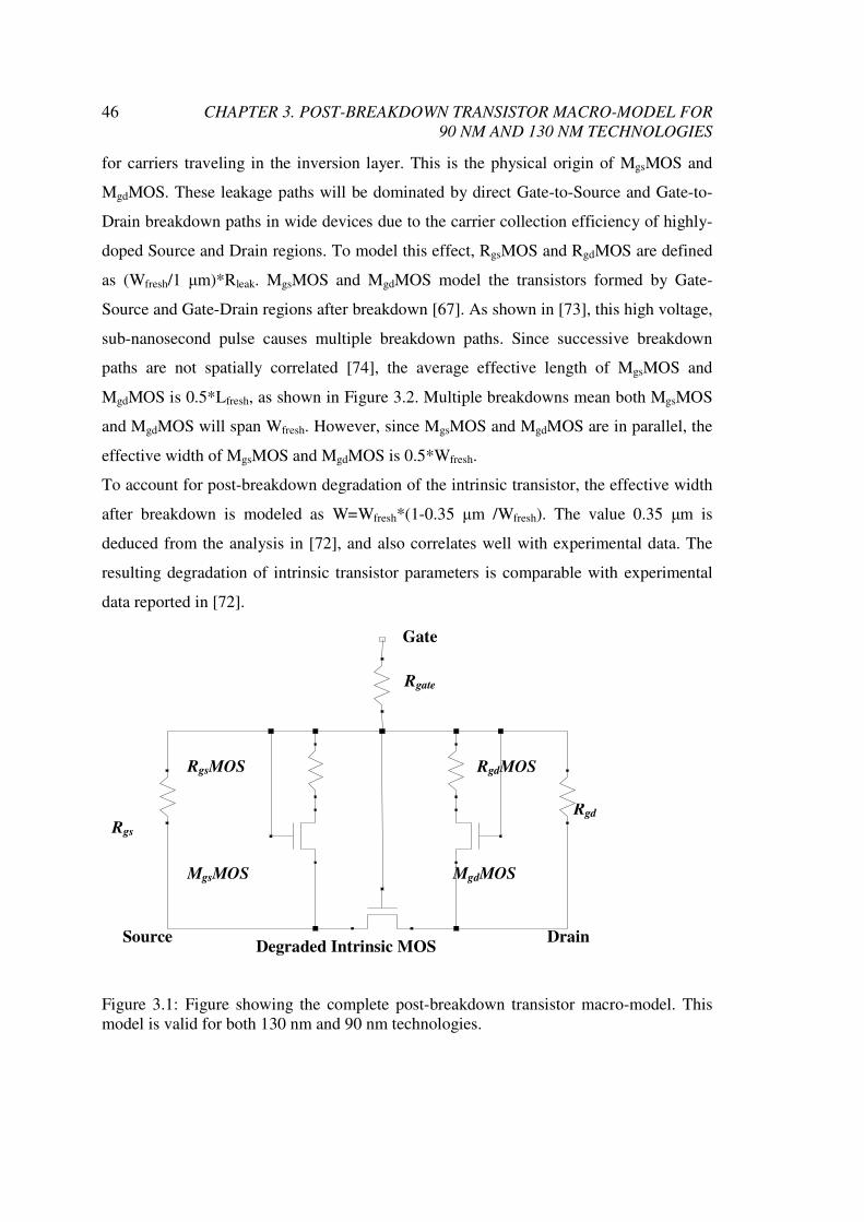
3.1.2 Macro-Model ................................................................................................... 45
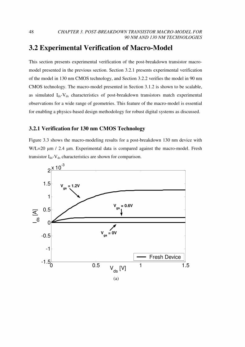
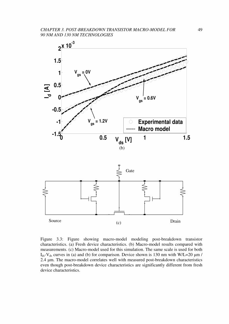
3.2 Experimental Verification of Macro-Model ........................................................... 48
3.2.1 Verification for 130 nm CMOS Technology................................................... 48
3.2.2 Verification for 90 nm CMOS Technology ..................................................... 53
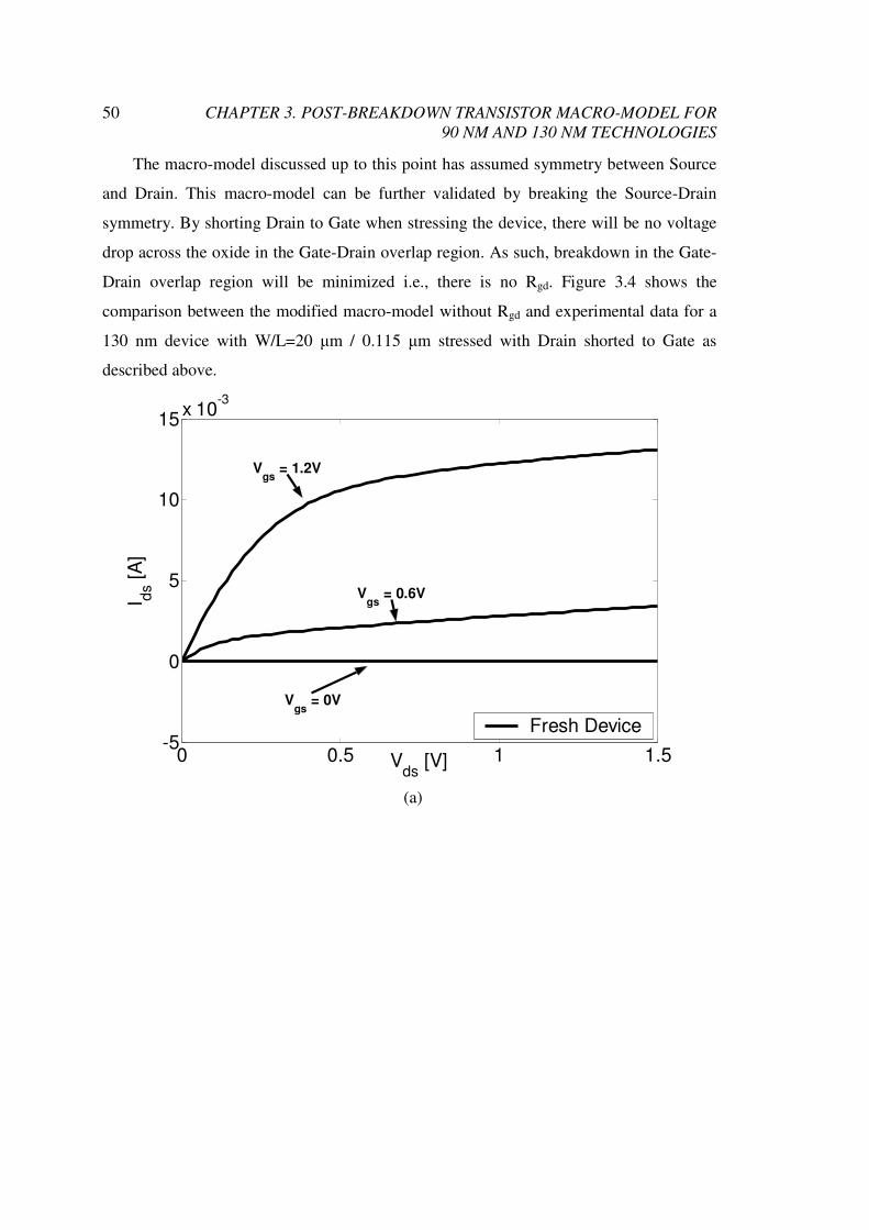
3.2.3 Macro-model Verification ............................................................................... 59
3.3 Chapter Summary ................................................................................................... 60
Chapter 4 Ultra-Fast Transmission Line Pulsing System........................................... 61
4.1 TLP and VFTLP Systems ....................................................................................... 62
4.2 Ultra-Fast Transmission Line Pulsing System........................................................ 63
4.2.1 UFTLP Architecture ........................................................................................ 65
4.2.2 UFTLP Performance........................................................................................ 66
4.2.3 Indirect Measurement of UFTLP..................................................................... 69
4.3 Gate Oxide Characterization with UFTLP ............................................................. 73
4.3.1 Experiments ..................................................................................................... 73
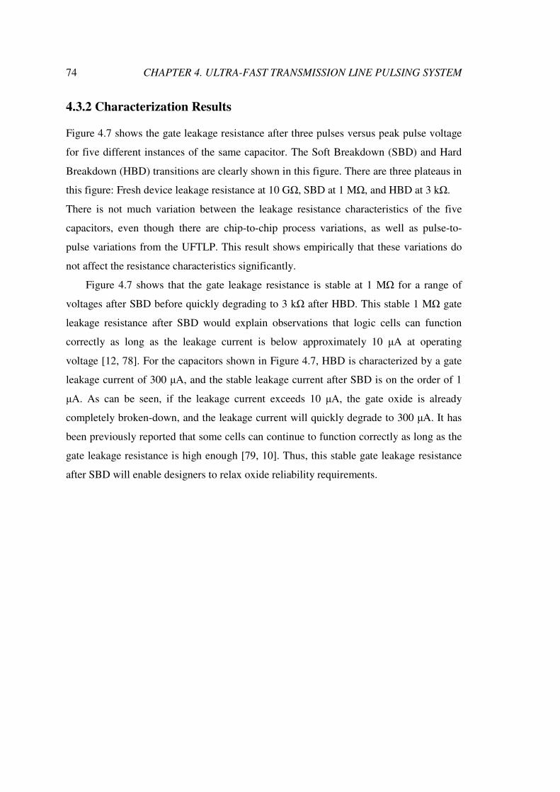
4.3.2 Characterization Results .................................................................................. 74
4.4 Chapter Summary ................................................................................................... 76
Chapter 5 Physics-Based Design Methodology for Digital Systems Robust to ESD-
CDM Events .................................................................................................................... 78
5.1 Chip-level Simulation ............................................................................................. 79
5.1.1 Digital Standard Cell Library Characterization ............................................... 79
5.1.2 Application Examples...................................................................................... 80
5.2 Correct-By-Construction Protection Strategy......................................................... 86
5.2.1 Protection Strategy........................................................................................... 86
5.2.2 Correct-By-Construction Protection Strategy Analysis Results ...................... 87
5.2.3 Correct-By-Construction Protection Strategy Simulation Results .................. 89
5.3 Physics-Based Design Methodology and Correct-By-Construction Protection
Strategy Silicon Results ................................................................................................ 91
5.4 Chapter Summary ................................................................................................... 92
Chapter 6 Conclusions.................................................................................................... 93
6.1 Summary of Dissertation ........................................................................................ 94
6.2 Recommendations for Future Work........................................................................ 95
Page 11
xi
6.3 Chapter Summary ................................................................................................... 97
Appendix A Scalable Thermal Model for 3-Dimensional SOI Technology............... 98
A.1 3D Technology....................................................................................................... 98
A.2 Thermal and Packaging Effects in 3D-SOI Technology ..................................... 100
A.3 Thermal Modeling and Electro-Thermal Simulations ......................................... 102
A.3.1 Experiments .................................................................................................. 102
A.3.2 Thermal Modeling......................................................................................... 105
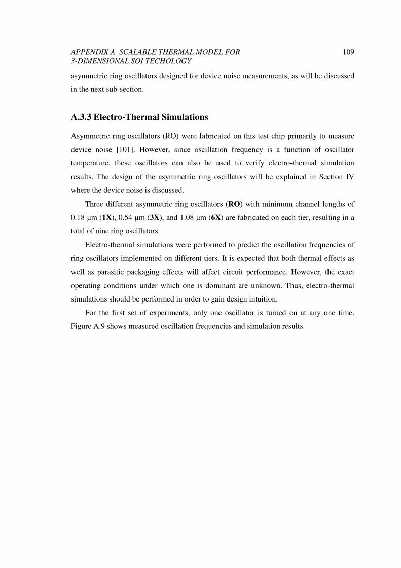
A.3.3 Electro-Thermal Simulations ........................................................................ 109
A.4 Device Noise ........................................................................................................ 113
A.4.1 Experiments .................................................................................................. 113
A.4.2 Discussion of Device Noise .......................................................................... 115
A.5 Chapter Summary ................................................................................................ 117
Bibliography .................................................................................................................. 120
Page 13
xiii
List of Tables
Table 2.1: Rgs for NMOS transistors. Entry with F indicates that the inverter chain fails to
operate correctly at time 0......................................................................................... 29
Table 2.2: Rgs for PMOS transistors. Entry with F indicates that the inverter chain fails to
operate correctly at time 0......................................................................................... 30
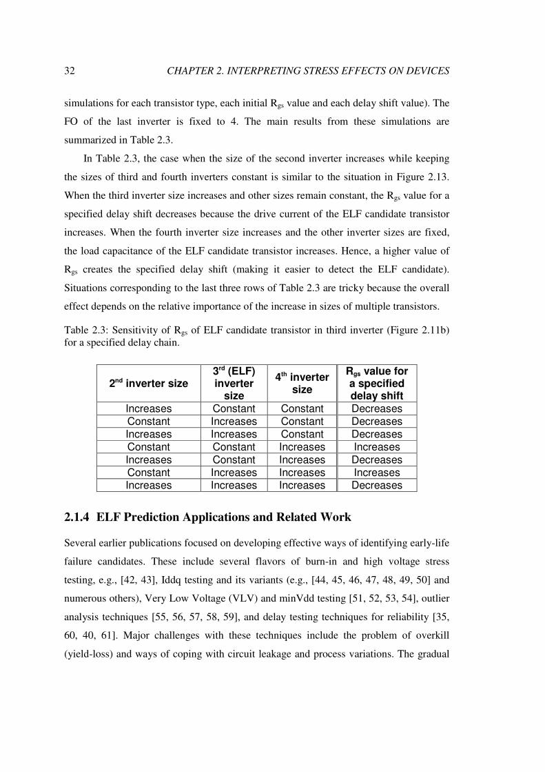
Table 2.3: Sensitivity of Rgs of ELF candidate transistor in third inverter (Figure 2.11b)
for a specified delay chain. ....................................................................................... 32
Table 2.4: Table summarizing the post-breakdown leakage resistance of 130 nm N Thin
Oxide capacitor after different stress conditions. It can be seen that different stress
conditions resulted in similar post-breakdown leakage resistance. .......................... 38
Table 3.1: Table summarizing the modeling methodology for the elements in Figure 3.1.
................................................................................................................................... 47
Table 3.2: Table summarizing macro-model accuracy..................................................... 59
Table 4.1: Switch positions for different modes of UFTLP. ............................................ 66
Table 4.2: Statistical variation of UFTLP for different line lengths................................. 68
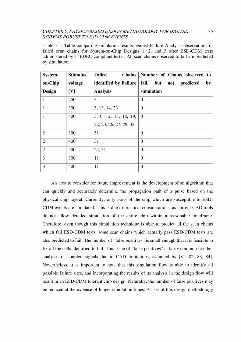
Table 5.1: Table comparing simulation results against Failure Analysis observations of
failed scan chains for System-on-Chip Designs 1, 2, and 3 after ESD-CDM tests
administered by a JEDEC-compliant tester. All scan chains observed to fail are
predicted by simulation............................................................................................. 85
Page 15
xv
List of Figures
Figure 1.1: The three stages of oxide breakdown: Defect Generation, Soft Breakdown and
Hard Breakdown (after reference [15])....................................................................... 5
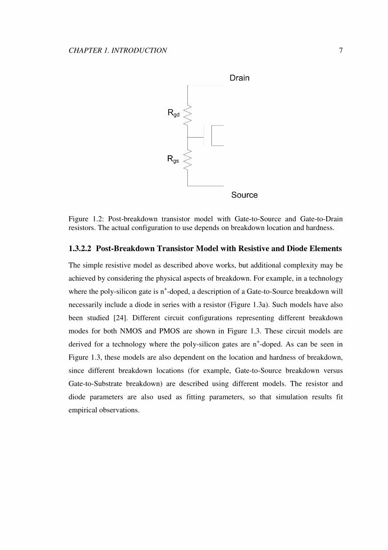
Figure 1.2: Post-breakdown transistor model with Gate-to-Source and Gate-to-Drain
resistors. The actual configuration to use depends on breakdown location and
hardness....................................................................................................................... 7
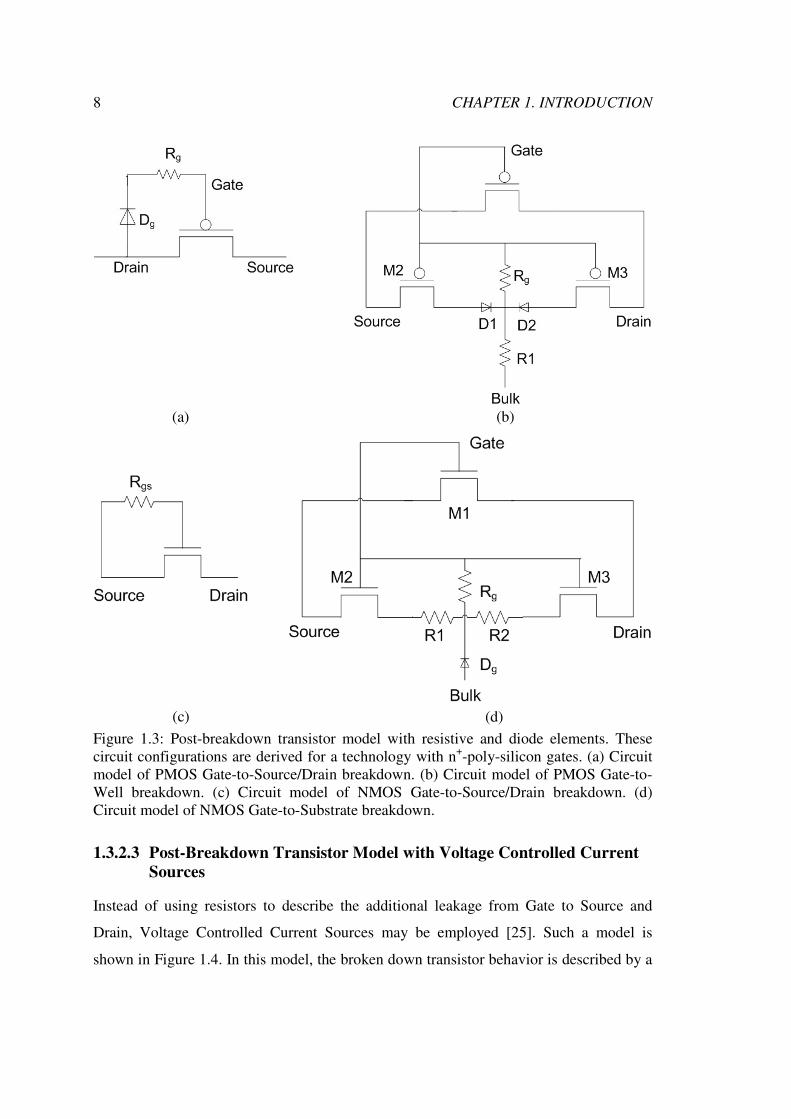
Figure 1.3: Post-breakdown transistor model with resistive and diode elements. These
circuit configurations are derived for a technology with n+-poly-silicon gates. (a)
Circuit model of PMOS Gate-to-Source/Drain breakdown. (b) Circuit model of
PMOS Gate-to-Well breakdown. (c) Circuit model of NMOS Gate-to-Source/Drain
breakdown. (d) Circuit model of NMOS Gate-to-Substrate breakdown. ................... 8
Figure 1.4: Post-breakdown transistor model using voltage controlled current sources.
Depending on breakdown location, either one or both of the current sources is
active. .......................................................................................................................... 9
Figure 2.1: Experimental test structure array.................................................................... 15
Figure 2.2: Experimental flow. ......................................................................................... 16
Figure 2.3: Gate current noise to indicate soft breakdown. .............................................. 17
Figure 2.4: Ids-Vds of an arbitrary transistor during various stages of stress after Soft
Breakdown (SBD). (a) Vgs = 1V. (b) Various Vgs values. Ids-Vds characteristics
degrade gradually until hard breakdown................................................................... 18
Figure 2.5: Gate oxide ELF-Rgs(t) model. (a) Rgs(t) at time t1. (b) Rgs(t) at time t2 > t1. .. 19
Page 16
xvi
Figure 2.6: Measured Ids-Vds characteristics vs. simulation using gate oxide ELF-Rgs(t)
model......................................................................................................................... 20
Figure 2.7: Rgs decreases with time until hard breakdown occurs. (a) Time evolution of
Rgs for the transistor in Fig. 2.4. (b) Normalized time evolution of Rgs for 6
transistors. (c) Time evolution of Rgs for two transistors of same geometry. Soft-
breakdown is induced in one of the transistors at time 0 (SBD transistor). (d) Gate
leakage current evolution for the transistor in Fig. 2.4. ............................................ 22
Figure 2.8: Relationship between Rgsmin and W/L........................................................... 23
Figure 2.9: Rgsmin/(Rgsmin + Rgate) for NMOS transistors. .............................................. 24
Figure 2.10: Circuit delay shift introduced by threshold voltage shift of a single stressed
transistor in the third stage of a seven-stage inverter chain. ..................................... 25
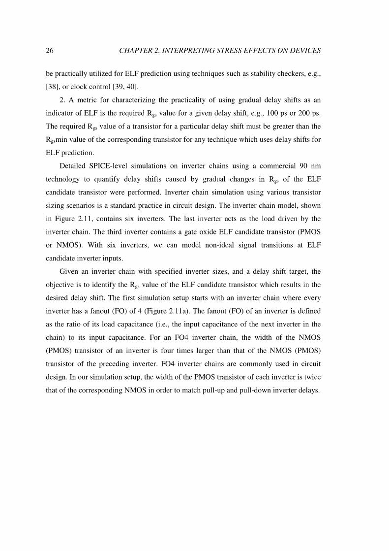
Figure 2.11: Six-stage inverter chain. (a) FO4 simulation. (b) Simulation to understand
the effects of transistor sizes. .................................................................................... 27
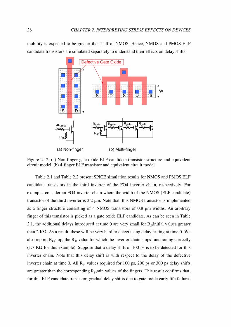
Figure 2.12: (a) Non-finger gate oxide ELF candidate transistor structure and equivalent
circuit model, (b) 4-finger ELF transistor and equivalent circuit model. ................. 28
Figure 2.13: (a) 2nd and 3rd stages of FO4 inverter chain of Figure 2.11a. (b) Equivalent
circuit when M2 is on. .............................................................................................. 31
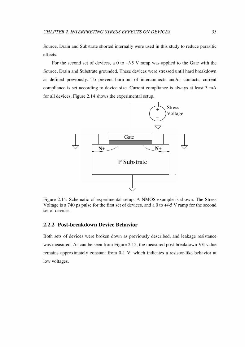
Figure 2.14: Schematic of experimental setup. A NMOS example is shown. The Stress
Voltage is a 740 ps pulse for the first set of devices, and a 0 to +/-5 V ramp for the
second set of devices................................................................................................. 35
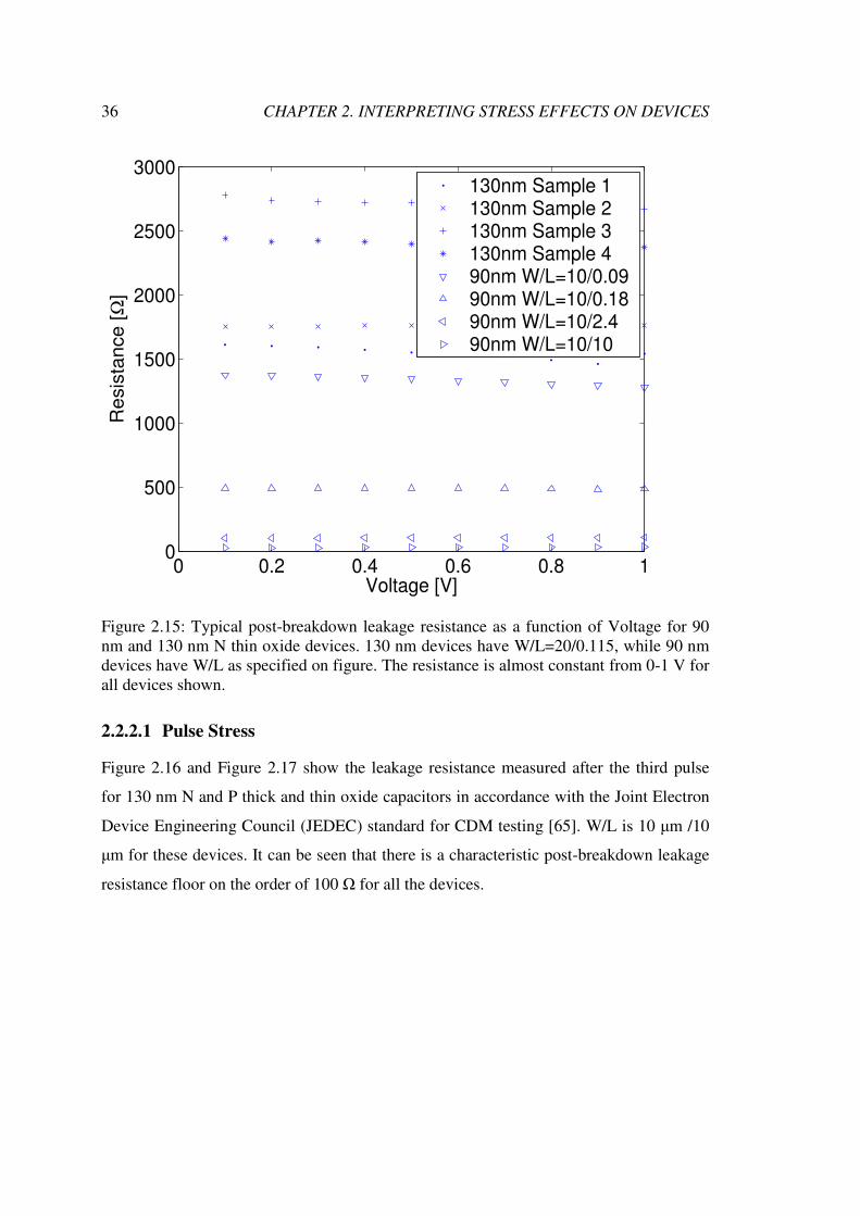
Figure 2.15: Typical post-breakdown leakage resistance as a function of Voltage for 90
nm and 130 nm N thin oxide devices. 130 nm devices have W/L=20/0.115, while 90
nm devices have W/L as specified on figure. The resistance is almost constant from
0-1 V for all devices shown. ..................................................................................... 36
Figure 2.16: Figure showing leakage resistance after the third pulse as a function of
Voltage across the Gate with the Source, Drain and Substrate grounded for 130 nm
N and P thin oxide devices. A post-breakdown leakage resistance floor of about 100
Ω is noted. ................................................................................................................. 37
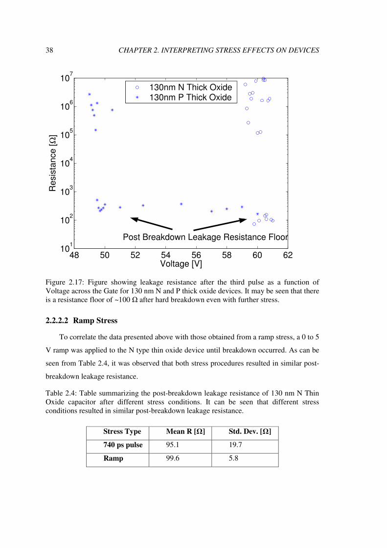
Figure 2.17: Figure showing leakage resistance after the third pulse as a function of
Voltage across the Gate for 130 nm N and P thick oxide devices. It may be seen that
Page 17
xvii
there is a resistance floor of ~100 Ω after hard breakdown even with further stress.
................................................................................................................................... 38
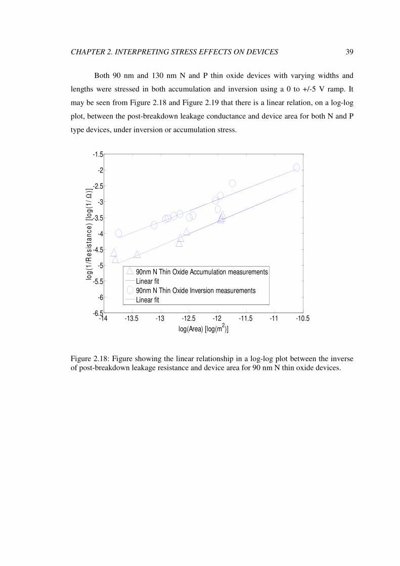
Figure 2.18: Figure showing the linear relationship in a log-log plot between the inverse
of post-breakdown leakage resistance and device area for 90 nm N thin oxide
devices....................................................................................................................... 39
Figure 2.19: Figure showing the linear relationship in a log-log plot between the post-
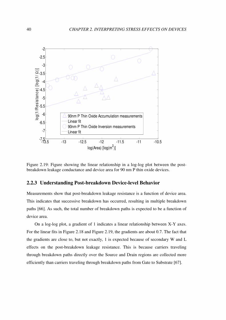
breakdown leakage conductance and device area for 90 nm P thin oxide devices... 40
Figure 3.1: Figure showing the complete post-breakdown transistor macro-model. This
model is valid for both 130 nm and 90 nm technologies. ......................................... 46
Figure 3.2: This figure shows the top-view of device Oxide area with Source at the top
and Drain at the bottom. The numbered circles represent breakdown locations. Each
breakdown location will form an MgsMOS and MgdMOS, each with its own Leffective.
Since breakdown locations are spatially uncorrelated, the aggregate Leffective for all
MgsMOS and MgdMOS is Lfresh/2. Since multiple MgsMOS and MgdMOS will span
Wfresh, the aggregate effective width for MgsMOS and MgdMOS is Wfresh/2, as
discussed in Section 3.1.2. ........................................................................................ 47
Figure 3.3: Figure showing macro-model modeling post-breakdown transistor
characteristics. (a) Fresh device characteristics. (b) Macro-model results compared
with measurements. (c) Macro-model used for this simulation. The same scale is
used for both Ids-Vds curves in (a) and (b) for comparison. Device shown is 130 nm
with W/L=20 µm / 2.4 µm. The macro-model correlates well with measured post-
breakdown characteristics even though post-breakdown device characteristics are
significantly different from fresh device characteristics........................................... 49
Figure 3.4: Figure showing macro-model results for transistors with no direct Gate-to-
Drain breakdown paths. (a) Fresh device characteristics. (b) Macro-model results
compared with measurements. (c) Macro-model used for this simulation. Device
shown is 130 nm with W/L=20 µm / 0.115 µm. Macro-model matches measured
data even if post-breakdown device is asymmetrical................................................ 51
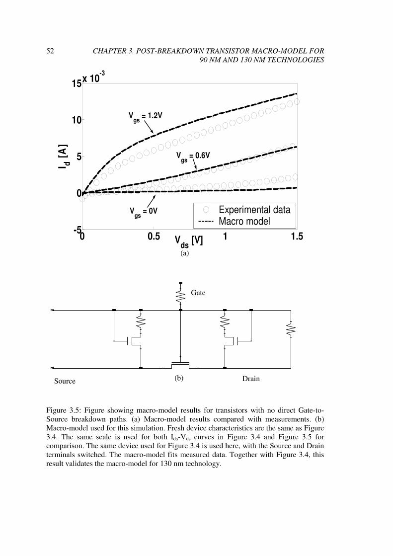
Figure 3.5: Figure showing macro-model results for transistors with no direct Gate-to-
Source breakdown paths. (a) Macro-model results compared with measurements. (b)
Macro-model used for this simulation. Fresh device characteristics are the same as
Page 18
xviii
Figure 3.4. The same scale is used for both Ids-Vds curves in Figure 3.4 and Figure
3.5 for comparison. The same device used for Figure 3.4 is used here, with the
Source and Drain terminals switched. The macro-model fits measured data.
Together with Figure 3.4, this result validates the macro-model for 130 nm
technology................................................................................................................. 52
Figure 3.6: Figure showing macro-model modeling post-breakdown transistor
characteristics. (a) Fresh device characteristics. (b) Macro-model results compared
with measurements. (c) Macro-model used for this simulation. The same scale is
used for both Ids-Vds curves for comparison. 90 nm device with W/L=2 µm / 0.1 µm
is shown. Macro-model matches measured post-breakdown characteristics even
though fresh device characteristics are very different. ............................................. 54
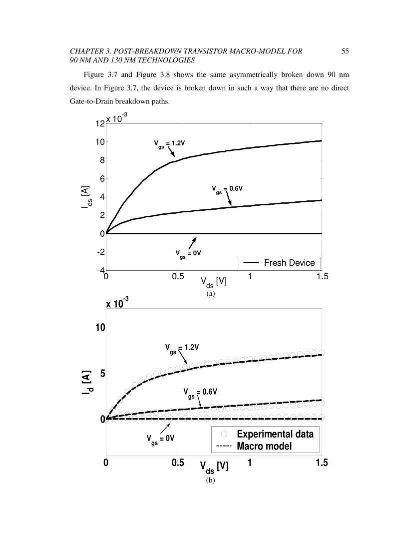
Figure 3.7: Figure showing macro-model results for transistors with no direct Gate-to-
Drain breakdown paths. (a) Fresh device characteristics. (b) Macro-model results
compared with measurements. (c) Macro-model used for this simulation. 90 nm
device with W/L=10 µm / 0.09 µm is shown. The macro-model is valid even if the
device breakdown is asymmetrical. .......................................................................... 56
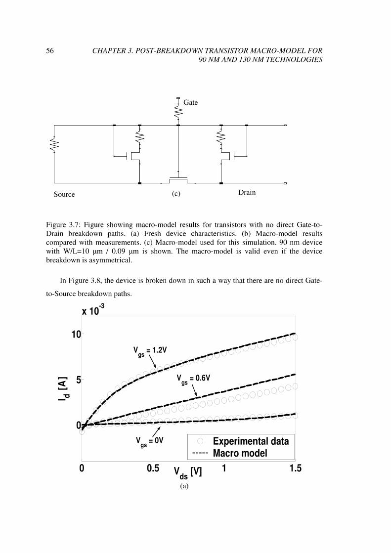
Figure 3.8: Figure showing macro-model results for transistors with no direct Gate-to-
Source breakdown paths. (a) Macro-model results compared with measurements. (b)
Macro-model used for this simulation. Fresh device characteristics are the same as
Figure 3.7. The same scale is used for both Ids-Vds curves in Figure 3.7 and Figure
3.8 for comparison. The same device used for Figure 3.7 is used here, with the
Source and Drain terminals switched. The macro-model fits measured data.
Together with Figure 3.7, this result validates the macro-model for 90 nm
technology................................................................................................................. 57
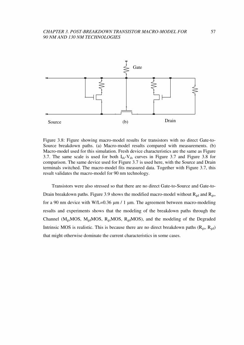
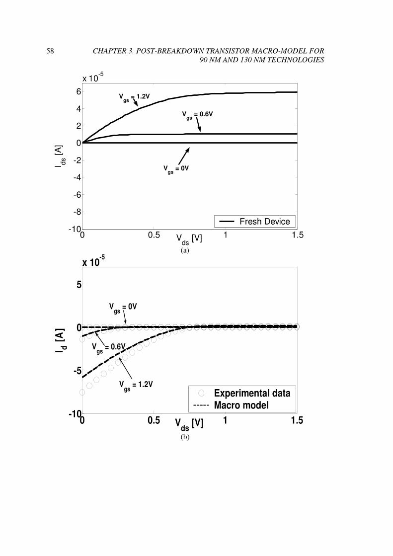
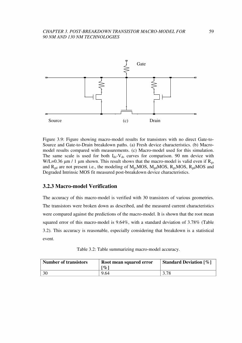
Figure 3.9: Figure showing macro-model results for transistors with no direct Gate-to-
Source and Gate-to-Drain breakdown paths. (a) Fresh device characteristics. (b)
Macro-model results compared with measurements. (c) Macro-model used for this
simulation. The same scale is used for both Ids-Vds curves for comparison. 90 nm
device with W/L=0.36 µm / 1 µm shown. This result shows that the macro-model is
valid even if Rgs and Rgd are not present i.e., the modeling of MgsMOS, MgdMOS,
Page 19
xix
RgsMOS, RgdMOS and Degraded Intrinsic MOS fit measured post-breakdown
device characteristics. ............................................................................................... 59
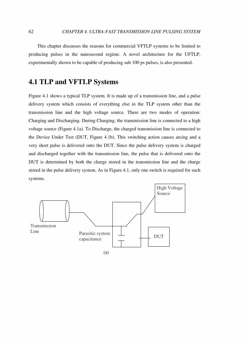
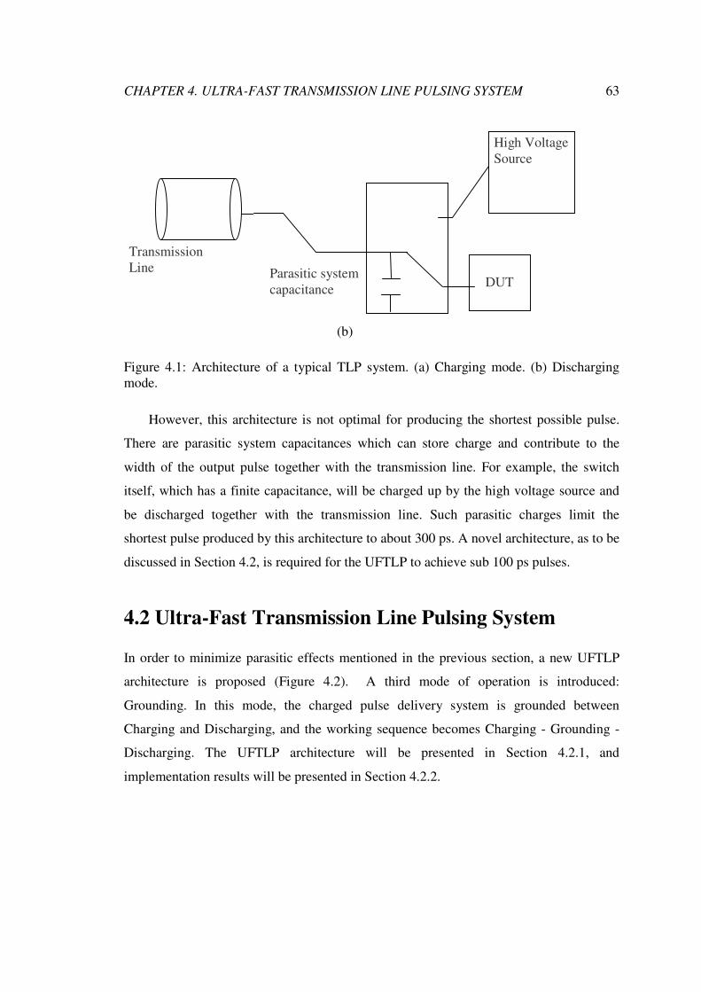
Figure 4.1: Architecture of a typical TLP system. (a) Charging mode. (b) Discharging
mode.......................................................................................................................... 63
Figure 4.2: Proposed architecture for UFTLP. (a) Charging Mode. (b) Grounding Mode.
(c) Discharging Mode. .............................................................................................. 64
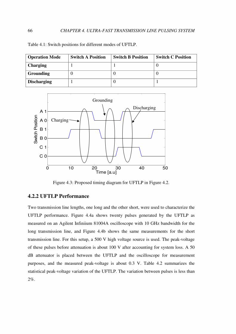
Figure 4.3: Proposed timing diagram for UFTLP in Figure 4.2. ...................................... 66
Figure 4.4: Plots showing 20 pulses from the UFTLP. (a) Long transmission line. (b)
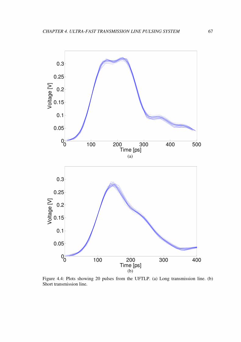
Short transmission line.............................................................................................. 67
Figure 4.5: (a) Ideal trapezoidal pulse with 150ps plateau and 25ps rise time. (b)
Comparison between calculated power spectrum and measured power spectrum of
long transmission line output pulse........................................................................... 70
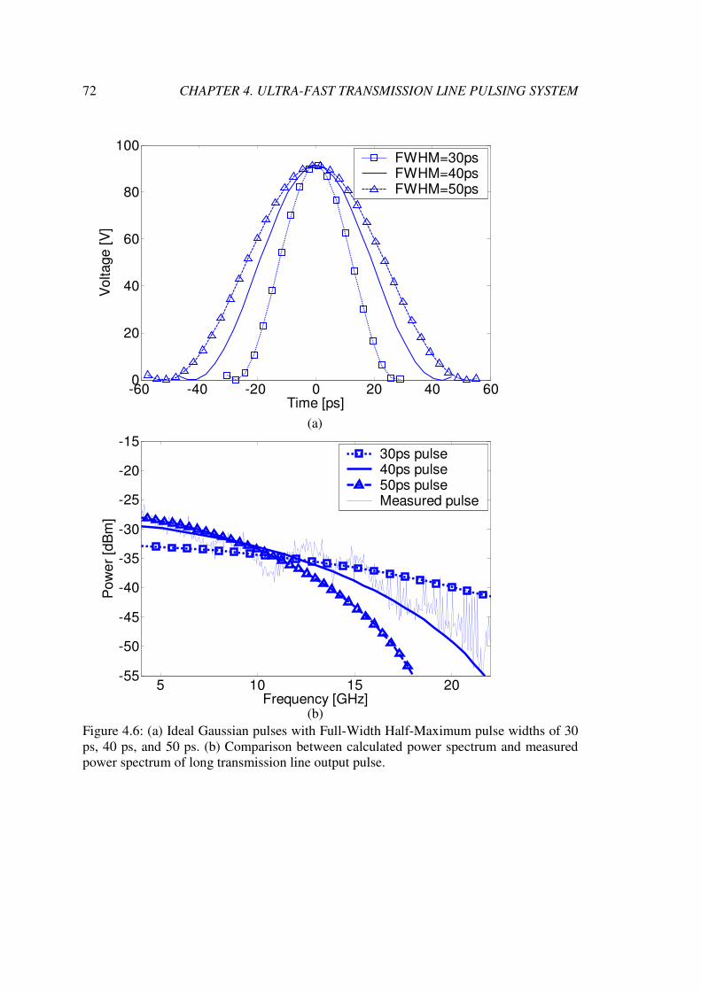
Figure 4.6: (a) Ideal Gaussian pulses with Full-Width Half-Maximum pulse widths of 30
ps, 40 ps, and 50 ps. (b) Comparison between calculated power spectrum and
measured power spectrum of long transmission line output pulse. .......................... 72
Figure 4.7: Figure showing gate leakage resistance after the third 175ps pulse for five
different instances of the same capacitor. ................................................................. 75
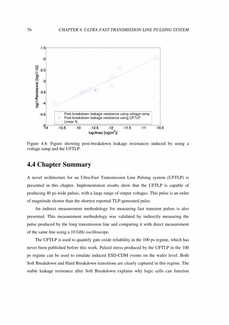
Figure 4.8: Figure showing post-breakdown leakage resistances induced by using a
voltage ramp and the UFTLP.................................................................................... 76
Figure 5.1: Figure showing the flow for digital standard cell library characterization. This
flow determines function failure of standard cells due to gate oxide breakdown..... 80
Figure 5.2: (a) SEM picture of gate identified to fail ESD-CDM test. Passive voltage
contrast shows marked poly-silicon gate to be leaky. (b) SEM picture of same gate
in (a), with poly-silicon layer removed to show damage in the diffusion region. .... 82
Figure 5.3: Figure showing flow for chip-level simulation of ESD-CDM events.
Simulation outputs scan chains and cells that have failed due to gate oxide
breakdown................................................................................................................. 83
Figure 5.4: Venn diagram showing the how scan chains are predicted to fail using the Fail
List and circuit simulation. ....................................................................................... 84
Figure 5.5: (a) Figure showing the insertion of a Ground Shield in between the IO traces
and the core traces. This technique is called Bottom Shielding. (b) Figure showing
Page 20
xx
the insertion of Ground Shields beside the IO traces. This technique is called Side
Shielding. .................................................................................................................. 87
Figure 5.6: Figure showing a simple case of a Ground Shield protecting a Victim Core
trace from an Aggressor IO trace. The schematic below is the analytical model of the
physical setup............................................................................................................ 88
Figure 5.7: Figure comparing estimated peak induced voltages on victim using the
analytic model and a full extraction as Ground Shield length, L, varies. The peak
induced voltage on the victim decreases as more ground shield protection is added,
as expected. ............................................................................................................... 89
Figure 5.8: Figure showing a partial schematic of the production IO trace pattern used to
validate the correct-by-construction protection strategy (not drawn to scale).......... 90
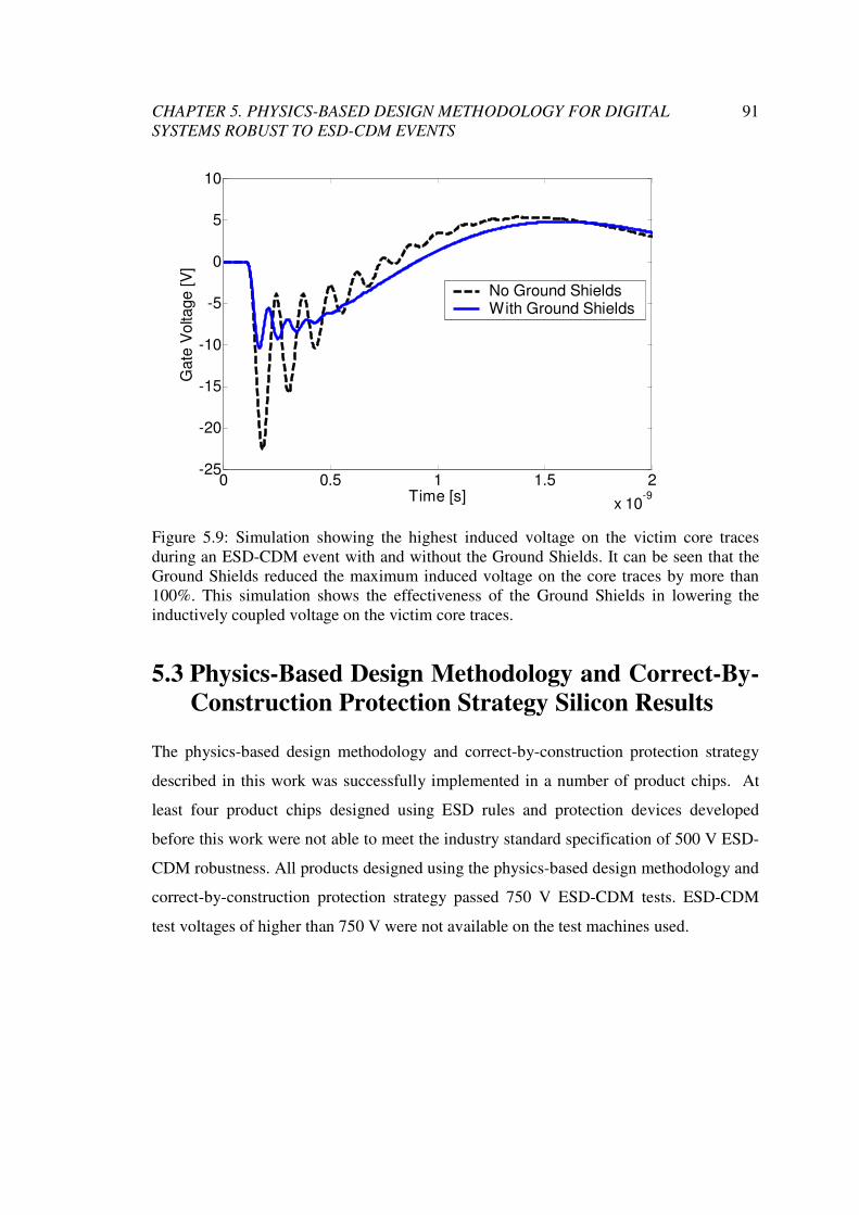
Figure 5.9: Simulation showing the highest induced voltage on the victim core traces
during an ESD-CDM event with and without the Ground Shields. It can be seen that
the Ground Shields reduced the maximum induced voltage on the core traces by
more than 100%. This simulation shows the effectiveness of the Ground Shields in
lowering the inductively coupled voltage on the victim core traces......................... 91
Figure A.1: Cross section of 3D-SOI technology (not shown to scale)............................ 99
Figure A.2: (a) Ids-Vds curve of 3D-SOI NMOS, with VGS of 1.5 V. W/L = 6 µm /0.2 µm.
The performance degradation of Tier B and C is mainly due to thermal effects. (b) I-
V curve of a 3D-SOI diode. Performance degradation of Tier A and B is due to 3D
packaging (through-wafer vias) and other parasitic resistive effects...................... 101
Figure A.3: Mapping of gate resistance as a function of temperature. With this
characterization, the gate resistance can be used to determine temperature when the
on-chip heat sources are turned on. The transistor shown has W/L = 6 µm / 0.2 µm,
and is on Tier C. Figure shown is a typical measurement. Each gate resistor
calibrated individually. ........................................................................................... 103
Figure A.4: (a) Layout of the DUT and the heat sources on each tier. Temperature of
DUT can be controlled with surrounding heat sources. DUT gate resistance is used
as a thermometer. (b) 3D view of test structures. Test structures stacked on top of
one another, and can be turned on or off individually to simulate different operating
conditions. ............................................................................................................... 104
Page 21
xxi
Figure A.5: Thermal test structure independently designed by research group at Lincoln
Laboratory [9]. Note that this test structure is ~4 times larger than the thermal test
structure in Figure A.4a. ......................................................................................... 105
Figure A.6: Thermal model used in this work. Power is the I × V product, and thermal
resistances shown.................................................................................................... 106
Figure A.7: Figures comparing temperatures predicted by thermal model with measured
temperatures. (a) Only one tier active at any one time. (b) All three tiers active at the
same time. ............................................................................................................... 107
Figure A.8: Comparison of temperatures predicted by thermal model with measured
temperatures using the thermal test structures designed by Lincoln Laboratory. Note
that the measured data agrees well with the results predicted by the thermal model
even though the power used in this circuit is much larger than the power used in the
Stanford test structures (Figure A.7)....................................................................... 108
Figure A.9: Electro-Thermal simulations compared against measured oscillation
frequencies for all three tiers. Only one oscillator is turned on at any one time for
(a) 1X. (b) 3X.......................................................................................................... 110
Figure A.10: Electro-Thermal simulations compared against measured oscillation
frequencies for all three tiers. All oscillators are turned on at the same time for (a)
1X. (b) 3X. .............................................................................................................. 111
Figure A.11: (a) Figure showing the asymmetric ring oscillator. Node A is the gate of the
small inverters, and Node B is the gate of the large inverters. (b) Circuit schematic
of the small inverter, and how Node A and B behaves. (c) Behavior of Node A and
B. Node A is driven by the large inverters, and the transition from low to high
happens very quickly. Node B is driven by a small inverter, and has a slower slew
rate compared to Node A, which is driven by a large inverter. .............................. 114
Figure A.12: Figure showing phase noise of asymmetric ring oscillator measured at the
1/f2 region................................................................................................................ 115
Figure A.13: Figure showing measured device noise for 1X devices and 3X devices.
Device noise in 3D technology compared with a comparable commercial 0.18 µm
CMOS technology. ................................................................................................. 117
Page 23
1
Chapter 1
Introduction
VLSI performance has increased by five orders of magnitude in the past three decades,
made possible by aggressive technology scaling [1]. This trend looks set to continue,
achieving integration capacity of billions of transistors in the near future. Foreseeable
barriers to future scaling include reliability, variability, and power. This dissertation
presents a physics-based design methodology and protection strategy for reliable digital
systems design. Reliability is first examined generally in Chapter 2, where it is shown
how understanding the physics (and thus behavior) of failing devices can enable design
methodologies such as online circuit failure prediction and burn-in reduction. Chapters 3
to 6 then focus on implementation details of a design methodology and protection
strategy for a particular aspect of reliability, namely, Electrostatic Discharge (ESD).
Although this implementation specifically deals with the design of a digital system robust
to ESD events, this physics-based design methodology may be easily adapted for other
reliability concerns such as Negative Bias Temperature Instability (NBTI).
1.1 Electrostatic Discharge
Electrostatic Discharge (ESD) is the balancing of charge between two objects at different
potential [2, 3]. ESD events may be observed in our daily lives. For example, static
Page 24
CHAPTER 1. INTRODUCTION
2
electricity may be generated due to friction between different materials, and the
accumulated electrostatic charge may be spontaneously transferred to another object at a
lower potential, either through direct contact or an induced electric field. A practical
situation may arise when a person generates electrostatic charge by walking on a carpeted
floor, and then discharges himself through a doorknob on a dry day. Such ESD events are
usually a mild shock to human beings, causing nothing more than mild discomfort.
However, if this same amount of ESD stress is injected into a chip, it could mean
catastrophic failure for the chip.
ESD events are high voltage (~ several kV) and high current (1 – 10 A) stress events
for microelectronic components. Despite the fact that ESD events are transient in nature
(> 100 ns in general), these events have been observed to cause catastrophic breakdown
in modern integrated circuits (ICs). In fact, a substantial number of IC failures are related
to ESD [4, 5, 6]. ESD damage accounts for nearly a third of all IC failures, and
approximately 10% of customer returns are related to ESD damage. As a result, ESD is
one of the most important quality and reliability concerns in the IC industry [7].
1.1.1 Electrostatic Discharge Protection Design
On the device level, the impact of technology on ESD robustness has been carefully
studied [8]. Technology choices, such as isolation structures, influence the electrical and
thermal performances of devices, and these influences have been carefully analyzed in
the design of ESD-robust devices given technology constraints. On the circuit level, ESD
protection circuits and devices, such as power rail clamps, have been extensively studied
[9]. Rules of thumbs for designing ESD protection have resulted from these extensive
fundamental studies, which leads to the perception that ESD engineering is a “black art”,
that ESD engineers provide solutions based on experience rather than a fundamental
understanding of failure mechanisms.
However, the rule-based approach to protection design is sub-optimal for several
reasons.
1. Firstly, the number of protection rules is increasing rapidly from technology node
to technology node. New reliability concerns appear with CMOS scaling, and
they are all addressed by protection rules.
Page 25
CHAPTER 1. INTRODUCTION
3
2. Secondly, these rules only protect against specific known threats. They do not
provide any protection for new and unknown threats, some of which are
inevitable consequences of technology scaling.
3. Thirdly, these rules are developed using test structures, and do not consider the
specific circuit being protected. At best, the rules developed using these general
test structures represent a worst case, with large safety margin. It is even possible
that inadequate rules are developed using these general test structures.
4. Finally, there are tradeoffs in the application of these rules. A clear understanding
of the circuit being protected is necessary so that appropriate tradeoffs are made.
In summary, it is possible that ESD damage can still occur even after faithfully
following all of the protection rules. Therefore, to rely on protection rules to provide
adequate ESD protection is to rely on the protection rules covering all the bases. If there
is but a single threat which was not addressed by the protection rules, product yield will
suffer, possibly leading to entire product lines that cannot be shipped to the customer in
the worst case.
1.2 Physics-Based Design Methodology
The competitive nature of the modern IC industry means that companies can ill-afford to
use product silicon as test structures. The cost of mask repair and silicon re-spin for
leading edge technologies can easily bankrupt smaller companies, and remove the
competitive edge from larger companies. Therefore, it is imperative that a more
comprehensive physics-based design methodology (as compared to rule-based
methodologies) be developed. This physics-based design methodology should consider
the system which is being protected, and protect against all reliability threats, both
expected and unexpected.
The reliability concern in this case is ESD. Therefore, the design methodology
should use the protected system itself to determine how the ESD event propagates
through the chip, and also if any damage was done. There are at least two different
possible strategies for ensuring reliable digital system design:
Page 26
CHAPTER 1. INTRODUCTION
4
1. The system may be designed such that no gate ever sees a voltage greater than the
breakdown voltage. This is a safe approach, since no catastrophic breakdown can
occur if nothing in the system ever sees a voltage greater than the breakdown
voltage.
2. The system may be designed such that it is possible for some gates to see a
voltage greater than the breakdown voltage during an ESD event. However, the
design methodology should ensure that no chip level function failure occurs, even
though it may be possible that some devices are damaged. This approach is more
“on the edge”. Even though it may appear counter-intuitive for a circuit to be
functioning with broken down devices at first, it has been shown empirically that
some circuits continue to operate even after the first breakdown has occurred [10,
11, 12, 13, 14].
The physics-based design methodology presented in this dissertation can be used for
both protection strategies, depending on the risk attitude of the designer.
For both strategies, a method to perform chip-level circuit simulations quickly
becomes essential. Chip-level circuit simulation is needed because the protected system is
used to determine the propagation path. Implementation details are covered in Chapter 5.
For implementing protection strategy number two, a post-breakdown transistor macro-
model is required (Chapter 3). This macro-model may be used to determine if the system
will experience function failure after specific transistors are damaged by ESD events.
1.3 Survey of Literature: Post-Breakdown Behavior
In order to develop the post-breakdown transistor macro-model as described above, it is
necessary to study the behavior of post-breakdown devices. Additional current leakage
paths are formed through the gate oxide after breakdown, and transistor current
characteristics are also modified. This sub-section surveys the post-breakdown
conduction models and post-breakdown transistor models available in literature.
Page 27
CHAPTER 1. INTRODUCTION
5
1.3.1 Post-Breakdown Conduction
The typical evolution of gate leakage current, Ig, during an oxide stress is shown in
Figure 1.1 [15]. Three stages are typically observed:
1. Defect Generation
2. Soft Breakdown
3. Hard Breakdown
Figure 1.1: The three stages of oxide breakdown: Defect Generation, Soft Breakdown and
Hard Breakdown (after reference [15]).
The first stage, Defect Generation, has been extensively studied [16, 17]. Defects
generated in thin oxides creates Stress Induced Leakage Current (SILC) that gradually
increases gate leakage current Ig. The end of this stage has been traditionally defined as
oxide failure, and has been extensively characterized.
The second stage, Soft Breakdown, has been an area of intense research in recent
years. Both gate leakage current and gate current noise are permanently increased in this
stage. During Soft Breakdown, Ig gradually increases, but is typically below 10 µA at 3
V, and 100 nA at 1.2 V for an oxide thickness of 15 A.
The third and final stage is Hard Breakdown. It has been shown that applying a
current compliance during a constant voltage stress arrests and freezes Hard Breakdown
[18, 19]. This phenomenon implies that Hard Breakdown has a time evolution,
Page 28
CHAPTER 1. INTRODUCTION
6
continuously progressing from an insulating state to a highly conductive state. This has
been confirmed in [20] and [21].
There are several models in the literature on the time evolution of post-breakdown
conduction. One model that explains the experimental characteristics of Soft Breakdown
conduction uses a Quantum Point Contact (QPC) to explain both Soft Breakdown and
Hard Breakdown [22]. Another model shows that the gate leakage current after SBD
increases gradually, and is finally limited by series resistance [23].
These different models available in the literature agree that post-breakdown
conductions evolve in time, and finally reach a steady resistance state after Hard
Breakdown. The post-breakdown leakage resistance measurements will be presented in
Chapter 2, where transistors were subjected to ESD stress conditions of interest to this
work.
1.3.2 Post-Breakdown Transistor Models
As mentioned previously, dielectric breakdown does not always lead to circuit failure. To
determine if circuits experience function failure after breakdown occurs, post-breakdown
transistor macro-models that can be implemented in circuit simulators are needed.
Several of these models are presented in this sub-section.
1.3.2.1 Post-Breakdown Transistor Model with Resistive Elements
Post-breakdown transistor behavior may be modeled by including resistors that go from
Gate-to-Source and Gate-to-Drain, depending on the location and hardness of breakdown
[10, 12] (Figure 1.2). Practically, this means that the resistors are chosen by trial and
error so that simulation results match empirical measurements. The resistors need not
necessarily have any physical significance. These models have been implemented in
circuit simulators, and were used to investigate circuit sensitivity to gate oxide
breakdowns.
Page 29
CHAPTER 1. INTRODUCTION
7
Figure 1.2: Post-breakdown transistor model with Gate-to-Source and Gate-to-Drain
resistors. The actual configuration to use depends on breakdown location and hardness.
1.3.2.2 Post-Breakdown Transistor Model with Resistive and Diode Elements
The simple resistive model as described above works, but additional complexity may be
achieved by considering the physical aspects of breakdown. For example, in a technology
where the poly-silicon gate is n+-doped, a description of a Gate-to-Source breakdown will
necessarily include a diode in series with a resistor (Figure 1.3a). Such models have also
been studied [24]. Different circuit configurations representing different breakdown
modes for both NMOS and PMOS are shown in Figure 1.3. These circuit models are
derived for a technology where the poly-silicon gates are n+-doped. As can be seen in
Figure 1.3, these models are also dependent on the location and hardness of breakdown,
since different breakdown locations (for example, Gate-to-Source breakdown versus
Gate-to-Substrate breakdown) are described using different models. The resistor and
diode parameters are also used as fitting parameters, so that simulation results fit
empirical observations.
Page 30
CHAPTER 1. INTRODUCTION
8
Figure 1.3: Post-breakdown transistor model with resistive and diode elements. These
circuit configurations are derived for a technology with n+-poly-silicon gates. (a) Circuit
model of PMOS Gate-to-Source/Drain breakdown. (b) Circuit model of PMOS Gate-to-
Well breakdown. (c) Circuit model of NMOS Gate-to-Source/Drain breakdown. (d)
Circuit model of NMOS Gate-to-Substrate breakdown.
1.3.2.3 Post-Breakdown Transistor Model with Voltage Controlled Current
Sources
Instead of using resistors to describe the additional leakage from Gate to Source and
Drain, Voltage Controlled Current Sources may be employed [25]. Such a model is
shown in Figure 1.4. In this model, the broken down transistor behavior is described by a
(a) (b)
(c) (d)
Page 31
CHAPTER 1. INTRODUCTION
9
standard, empirical and analytical model [26] together with a Voltage Controlled Current
Source (VCCS) [27] to account for the additional breakdown path. Two Voltage
Controlled Current Sources are used, with one going from Gate-to-Source and the other
from Gate-to-Drain. Depending on the breakdown location, either one or both of the
current sources should be active.
Figure 1.4: Post-breakdown transistor model using voltage controlled current sources.
Depending on breakdown location, either one or both of the current sources is active.
1.3.2.4 Physics-Based Post-Breakdown Transistor Macro-Model
All of the models presented above can be implemented in a circuit simulator, and be used
to evaluate circuit sensitivity to breakdown events. Specifically, a circuit containing both
functional and broken down transistors simultaneously may be simulated to determine if
functional failure has occurred.
However, all of the models presented above have the same shortcomings. Namely,
they have different circuit configurations depending on breakdown location and hardness
and fitting parameters found by trial and error. These shortcomings make them unsuitable
choices in a chip-level simulation. A scalable post-breakdown transistor macro-model is
needed for chip-level simulation because there are transistors of various geometries in a
system. It is impossible to individually characterize every transistor with its own unique
fitting parameter. Furthermore, a unified macro-model that is independent of breakdown
location and hardness will simplify pre-processing, thereby reducing simulation time. A
novel post-breakdown transistor macro-model with these desirable characteristics is
developed for this work, and is presented in Chapter 3.
Page 32
CHAPTER 1. INTRODUCTION
10
1.4 Organization
This chapter has addressed the importance of reliability in modern VLSI, and also
provided background information about Electrostatic Discharge (ESD) events. A survey
of previous work on post-breakdown conduction and transistor modeling is also
presented. From this point on, this dissertation is organized as follows.
A general view of reliability is presented in Chapter 2. Transistors were broken down
and their behavior is studied. Knowing how devices behave when they are beginning to
fail enables development of design techniques such as online circuit failure prediction
and burn-in reduction, which are discussed in detail in Chapter 2. In addition, a stable
post-breakdown leakage resistance related to transistor geometry is reported. This
observation will be used in the development of a scalable post-breakdown transistor
macro-model.
Chapter 3 presents a physics-based post-breakdown transistor macro-model. No
fitting parameters are used in this macro-model, since the model is borne out of physical
considerations. Furthermore, this scalable macro-model can be used for all transistor
geometries typically used in system design, and accounts for both gate leakage and
degradation of intrinsic MOS parameters, such as transconductance, after breakdown.
This macro-model is used to analyze circuit sensitivity to breakdown events (Chapter 5),
and simulated results match experimental observations, validating the macro-model.
An Ultra-Fast Transmission Line Pulsing system (UFTLP) is presented in Chapter 4.
This system is capable of producing sub-100 ps pulses. It was observed that coupling
effects during ESD events are capable of producing destructive pulses that can break
down gate oxides. In particular, these coupling effects are most pronounced in ESD-
CDM (Electrostatic Discharge – Charged Device Model) events. The induced pulses have
pulse widths of approximately 100 ps. Commercial Transmission Line Pulsing (TLP) and
Very-Fast Transmission Line Pulsing (VFTLP) systems are limited to 1 ns pulse widths
due to architecture limitations. A new UFTLP architecture is proposed, and sub-100 ps
pulses were achieved. The UFTLP is then used to measure gate oxide breakdown
voltages in the 100 ps regime.
Page 33
CHAPTER 1. INTRODUCTION
11
In Chapter 5, a physics-based design methodology and protection strategy is
presented. This design methodology uses the macro-model from Chapter 3, and the gate
oxide breakdown voltages measured in Chapter 4.
1. The macro-model is used to characterize a specific digital standard cell library. In
this procedure, the macro-model replaces each transistor of a particular standard
cell in turn. The modified standard cell is then simulated to determine if
functional failure has occurred. This procedure is repeated for all the standard
cells. After this characterization, the overall sensitivity of the given standard cells
to ESD events can be determined.
2. SPICE netlists of three different System-on-Chip (SoC) designs have been
extracted. ESD-CDM events can be simulated using these netlists. These
simulations reveal the voltages seen at all the internal nodes during the ESD
event. With the breakdown voltages measured in Chapter 4, it is possible to
predict which gate oxides will be damaged by the ESD-CDM events.
3. Given that gate oxide vulnerabilities to ESD-CDM events has been identified,
several protection strategies are possible, including:
a. Design the system such that no gate oxide sees a voltage greater than the
breakdown voltage during ESD events.
b. Design the system such that chip-level function failure does not occur
after ESD events.
These design strategies are discussed, and a “correct-by-construction” protection
strategy is then presented. This physics-based design methodology and protection
strategy was successfully integrated into mainstream product design flow at LSI
Corporation using a commercial process. No ESD-related failures were observed for a
set of products designed using this methodology and protection strategy.
Finally, Chapter 6 draws conclusions from this work and suggests several possible
directions for future research in this area.
Page 34
CHAPTER 1. INTRODUCTION
12
1.5 Chapter Summary
The increase in VLSI performance is made possible by aggressive CMOS scaling. One
foreseeable barrier for future scaled CMOS technologies is reliability. This dissertation
presents a physics-based design methodology and protection strategy for reliable digital
systems design. In this work, the design methodology has been adapted to address ESD
reliability.
In the physics-based design methodology, the system being protected is used to
determine the propagation path of ESD events. While it is possible to design a system in
which none of its components see a voltage greater than the breakdown voltage during
ESD events, another possible design strategy is to ensure that the system does not
experience functional failure after ESD events. This is a feasible strategy as it has been
shown that gate oxide breakdown does not mean circuit function failure. The design
methodology presented in this dissertation can be used for both design strategies.
However, in order to ensure that the system does not experience functional failure after
ESD events, a thorough understanding of device-level post-breakdown behavior is
required. A survey of post-breakdown conduction models and post-breakdown transistor
models available in the literature is also briefly presented.
Page 35
13
Chapter 2
Interpreting Stress Effects on Devices
Investigations of both pre-breakdown and post-breakdown device-level behavior are
presented in this chapter. In this work, pre-breakdown devices are defined as those
having well-defined cut-off, linear, and saturation regions of operations. Post-breakdown
devices exhibit a resistor-like current characteristic. Characteristics of both pre- and post-
breakdown devices are identified, and possible ways to make use of these characteristics
in order to design reliable systems are suggested.
2.1 Using Pre-Breakdown Device-Level Behavior to
Predict Early Life Failure
There are several kinds of manufacturing defects which cause Early Life Failure (ELF)
and thus affect product yield. These defects include partial voids, inter-layer dielectric
(ILD) defects, and gate oxide defects such as exceptionally high numbers of broken
bonds. In addition to manufacturing defects, defects in gate oxide can also be introduced
during normal circuit operation, such as during EOS/ESD events or NBTI. This section
looks at how transistors with defective gate oxides behave.
Pre-breakdown devices, as defined in this work, clearly exhibit well-defined cut-off,
linear, and saturation regions of operations after constant voltage stress. Pre-breakdown
Page 36
CHAPTER 2. INTERPRETING STRESS EFFECTS ON DEVICES
14
devices are used to emulate transistors with defective gate oxides. It was found in this
study that the drive current of a stressed, pre-breakdown transistor degrades gradually,
until hard breakdown occurs and the transistor loses useful transistor characteristics. This
phenomenon results in gradual increase in delays of digital circuits containing these
stressed, pre-breakdown transistors before functional failure occurs. This result is
significant because these gradual delay shifts are large enough to be practically sensed by
inexpensive digital techniques. It is also worthwhile to note here that delay shifts do not
necessarily cause delay faults.
Knowledge of how devices behave when they are beginning to fail will enable
failure-prediction strategies, some of which are suggested in Section 2.1.4.
2.1.1 Experimentally Verified Gate Oxide ELF Model: ELF-Rgs(t)
Model
A test chip containing our array test devices (Figure 2.1) is manufactured by a
commercial foundry in 90 nm technology. The array contains ten 90 nm NMOS
transistors with lengths ranging from 0.1 µm to 2.1 µm and widths from 0.13 µm to 10
µm. These dimensions are representative of transistors used in actual 90 nm designs, and
also provide a range of geometries so that the results from this study can be more broadly
applicable. The oxide thickness is 1.6 nm, and the nominal supply voltage is 1 V. The
transistors share a common Bulk terminal. Individual Gate, Source, and Drain terminals
of each transistor are accessible. While the focus is on NMOS transistors in this section,
our measurements indicate similar behavior for PMOS transistors on the same test chip.
Hence, PMOS measurement results are not repeated.
Page 37
CHAPTER 2. INTERPRETING STRESS EFFECTS ON DEVICES
15
Figure 2.1: Experimental test structure array.
The experiment flow is described in Figure 2.2. For each transistor, the experiment
consists of two major stages:
1. Soft breakdown: Soft breakdown is induced in the gate oxide to emulate defective
gate oxide behavior. Since the test chip contains very few transistors, the
manufacturing process cannot be relied upon to produce transistors with defective
gate oxide. Hence, soft breakdown was induced in order to increase the density of
gate oxide defects (compared to fresh oxide). This approximation relies on a defective
gate oxide to contain more broken Si-Si bonds compared to defect-free gate oxide
[28]. Such an approximation of defective gate oxide using soft breakdown has been
used in the past (e.g., [29]). For this experiment, stress voltage of 3.4 V (chosen
empirically to induce soft breakdown within 10 minutes) is applied to the gate of a
transistor with all the other terminals grounded, and the gate current noise is
monitored. The stress is stopped when there is a sudden increase in gate current noise,
which is a reliable indicator of soft breakdown (Figure 2.3) [30, 31, 32]. Gate current
noise is defined as:
Common
Bulk
Drain
Gate
Source
Source
Drain
Gate Common Bulk
Page 38
CHAPTER 2. INTERPRETING STRESS EFFECTS ON DEVICES
16
22
2
meas meas
meas
I IGateCurrentNoise
I
−=
, where <x> represents the moving average of the
quantity x over five points. Imeas is the gate leakage current when 3.4 V is applied to the
gate.
2. High-voltage stress with periodic Ids-Vds measurement under nominal voltage
conditions: The transistor is stressed by applying a DC stress voltage between 2.7 V - 3.2
V (depending on oxide area) to its Gate with Source, Drain and Bulk terminals grounded.
This stress level is chosen empirically so that complete hard breakdown occurs in a few
days. The voltage stress is interrupted every ten minutes, and Ids-Vds characteristics are
measured by grounding the Bulk and Source terminals, and sweeping the Drain terminal
in steps of 100 mV. The Gate voltage is swept from 0 to 1 V in steps of 200 mV. This
procedure is continued until the transistor no longer has well-defined cutoff, linear, and
saturation regions, and breaks down into resistor-like behavior. In this work, this situation
is referred to as hard breakdown.
Stress transistor at 2.7V-3.2V for 10 minutes
Stop stress and measure Ids-Vds characteristics
Hard Breakdown.Stop for this transistor
Yes No
Ids-Vds characteristics resistor-like?
Repeat for all transistors
Stress fresh transistor at 3.4Vuntil Soft Breakdown, monitoredby Gate Current Noise
Figure 2.2: Experimental flow.
Page 39
CHAPTER 2. INTERPRETING STRESS EFFECTS ON DEVICES
17
0 100 200 30010
-10
10-5
100
Time [s]
Ga
te C
urr
en
t N
ois
e [(δ
I/I)
2]
Figure 2.3: Gate current noise to indicate soft breakdown.
Figure 2.4a shows measured Ids-Vds characteristics (Vgs = 1 V) of an arbitrary
transistor at various points of time during this experiment: 1. Fresh oxide; 2. Right after
soft breakdown (SBD) to emulate a gate oxide ELF candidate; 3. 3,000 minutes after
SBD; 4. Right before hard breakdown (5,890 minutes after soft breakdown); and, 5.
Immediately after hard breakdown. Figure 2.4b shows the characteristics of the same
transistor for various values of Vgs. It is clear that transistor Ids-Vds characteristics
gradually degrade with stress time. This gradual degradation is observed for all
transistors studied in this experiment.
Sudden increase in gate
current noise indicates
soft breakdown
Page 40
CHAPTER 2. INTERPRETING STRESS EFFECTS ON DEVICES
18
0 0.2 0.4 0.6 0.8 10
1
2
3
4
5
6
7
8x 10
-3
Vds
[V]
I ds [
A]
Fresh Gate OxideAfter Soft Breakdown (SBD)After 3000 minutesAfter 5890 minutesAfter 5900 minutes, Hard Breakdown (HBD)
0 0.2 0.4 0.6 0.8 10
1
2
3
4
5
6
7
8x 10
-3
Vds
[V]
I ds [
A]
Fresh Gate OxideAfter Soft Breakdown (SBD)After 3000 minutesAfter 5890 minutesAfter 5900 minutes, Hard Breakdown (HBD)
Figure 2.4: Ids-Vds of an arbitrary transistor during various stages of stress after Soft
Breakdown (SBD). (a) Vgs = 1V. (b) Various Vgs values. Ids-Vds characteristics degrade
gradually until hard breakdown.
Figure 2.5 summarizes the gate oxide ELF-Rgs(t) transistor model derived from the
experimental data. Rgate is the resistance of the gate poly-silicon, and is dependent on the
geometry of the transistor. It is directly proportional to the ratio of transistor width to
Hard
breakdown
(a)
(b)
Page 41
CHAPTER 2. INTERPRETING STRESS EFFECTS ON DEVICES
19
length (W/L). Rgs(t) is the transistor Gate-to-Source resistance at time instant t. From our
experimental data, this parameter is used to modify the Ids-Vds behavior of a defect-free
transistor to match the measured Ids-Vds behavior of a transistor at time = t units after soft
breakdown. In spite of similarities with traditional resistive gate oxide short models such
as [33, 10, 34, 35, 36, 37, 31], the gate oxide ELF-Rgs(t) is distinct because it introduces
the time parameter. The time parameter allows the modeling of “changes in Rgs over
time” for effective gate oxide early-life failure candidate identification. Note that this
model is also applicable for PMOS transistors.
Figure 2.5: Gate oxide ELF-Rgs(t) model. (a) Rgs(t) at time t1. (b) Rgs(t) at time t2 > t1.
Figure 2.6 compares measured Ids-Vds characteristics of a post-soft-breakdown
transistor with modeling results. The gate oxide ELF-Rgs(t) model is able to fit measured
Ids-Vds results to greater than 90% accuracy. At a given time instant t, a single Rgs value is
used to fit the measured transistor characteristics at that instant for all Vgs values.
Rgate
Source
Drain
Intrinsic
NMOS
Gate
Rgs(t1)
Rgate
Source
Drain
Intrinsic
NMOS
Gate
Rgs(t2) <
Rgs(t1)
For t2 > t1
(a) (b)
Page 42
CHAPTER 2. INTERPRETING STRESS EFFECTS ON DEVICES
20
0 0.2 0.4 0.6 0.8 1
0
1
2
3
4
5x 10
-3
Vds
[V]
I ds [
A]
After 5890 minutesELF-R
gs(t) Model
Figure 2.6: Measured Ids-Vds characteristics vs. simulation using gate oxide ELF-Rgs(t)
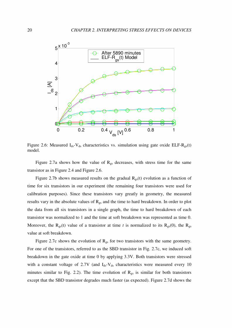
model.
Figure 2.7a shows how the value of Rgs decreases, with stress time for the same
transistor as in Figure 2.4 and Figure 2.6.
Figure 2.7b shows measured results on the gradual Rgs(t) evolution as a function of
time for six transistors in our experiment (the remaining four transistors were used for
calibration purposes). Since these transistors vary greatly in geometry, the measured
results vary in the absolute values of Rgs and the time to hard breakdown. In order to plot
the data from all six transistors in a single graph, the time to hard breakdown of each
transistor was normalized to 1 and the time at soft breakdown was represented as time 0.
Moreover, the Rgs(t) value of a transistor at time t is normalized to its Rgs(0), the Rgs
value at soft breakdown.
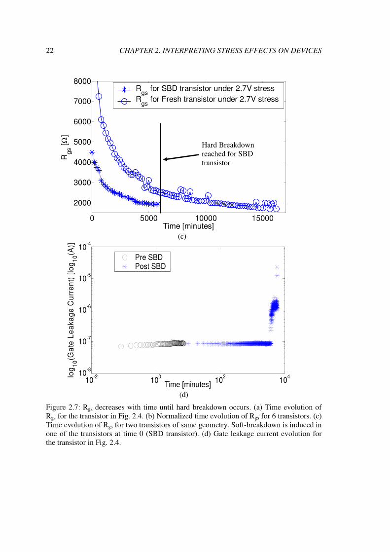
Figure 2.7c shows the evolution of Rgs for two transistors with the same geometry.
For one of the transistors, referred to as the SBD transistor in Fig. 2.7c, we induced soft
breakdown in the gate oxide at time 0 by applying 3.3V. Both transistors were stressed
with a constant voltage of 2.7V (and Ids-Vds characteristics were measured every 10
minutes similar to Fig. 2.2). The time evolution of Rgs is similar for both transistors
except that the SBD transistor degrades much faster (as expected). Figure 2.7d shows the
Page 43
CHAPTER 2. INTERPRETING STRESS EFFECTS ON DEVICES
21
gate leakage current evolution for the transistor shown in Figure 2.4 and Figure 2.6. It can
be seen that Hard Breakdown has a much more significant impact on gate leakage current
than Soft Breakdown.
0 2000 4000 6000 80001500
2000
2500
3000
3500
4000
4500
Rg
s [
Ω]
Time after soft breakdown [minutes]
Rgs
Time Evolution after Soft Breakdown
0 0.2 0.4 0.6 0.8 10
0.2
0.4
0.6
0.8
1
Normalized Time after Soft Breakdown
No
rma
lize
d R
gs
NMOS 1 DataNMOS 2 DataNMOS 3 DataNMOS 4 DataNMOS 5 DataNMOS 6 Data
Rgsmin
Hard
Breakdown
(a)
(b)
Page 44
CHAPTER 2. INTERPRETING STRESS EFFECTS ON DEVICES
22
0 5000 10000 15000
2000
3000
4000
5000
6000
7000
8000
Rgs [
Ω]
Time [minutes]
Rgs
for SBD transistor under 2.7V stress
Rgs
for Fresh transistor under 2.7V stress
10-2
100
102
104
10-8
10-7
10-6
10-5
10-4
Time [minutes]
log
10(G
ate
Le
aka
ge
Cu
rre
nt)
[lo
g1
0(A
)]
Pre SBDPost SBD
(d)
Figure 2.7: Rgs decreases with time until hard breakdown occurs. (a) Time evolution of
Rgs for the transistor in Fig. 2.4. (b) Normalized time evolution of Rgs for 6 transistors. (c)
Time evolution of Rgs for two transistors of same geometry. Soft-breakdown is induced in
one of the transistors at time 0 (SBD transistor). (d) Gate leakage current evolution for
the transistor in Fig. 2.4.
(c)
Hard Breakdown
reached for SBD
transistor
Page 45
CHAPTER 2. INTERPRETING STRESS EFFECTS ON DEVICES
23
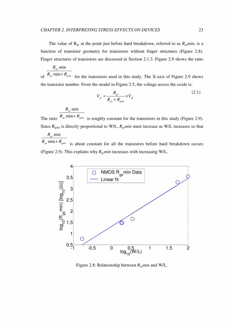
The value of Rgs at the point just before hard breakdown, referred to as Rgsmin, is a
function of transistor geometry for transistors without finger structures (Figure 2.8).
Finger structures of transistors are discussed in Section 2.1.3. Figure 2.9 shows the ratio
of
min
min
gs
gs gate
R
R R+ for the transistors used in this study. The X-axis of Figure 2.9 shows
the transistor number. From the model in Figure 2.5, the voltage across the oxide is:
gs
ox gs
gs gate
RV V
R R= ×
+
(2.1)
The ratio
min
min
gs
gs gate
R
R R+ is roughly constant for the transistors in this study (Figure 2.9).
Since Rgate is directly proportional to W/L, Rgsmin must increase as W/L increases so that
min
min
gs
gs gate
R
R R+ is about constant for all the transistors before hard breakdown occurs
(Figure 2.9). This explains why Rgsmin increases with increasing W/L.
-1 -0.5 0 0.5 1 1.5 20.5
1
1.5
2
2.5
3
3.5
4
log10
(W/L)
log
10(R
gsm
in)
[lo
g1
0( Ω
)]
NMOS Rgs
min Data
Linear fit
Figure 2.8: Relationship between Rgsmin and W/L.
Page 46
CHAPTER 2. INTERPRETING STRESS EFFECTS ON DEVICES
24
0 1 2 3 4 5 6 70.5
0.6
0.7
0.8
0.9
1
1.1
Rgsm
in/(
Rg
sm
in +
Rga
te)
Index
NMOS DataAverage R
gsmin/(R
gsmin + R
gate)
Figure 2.9: Rgsmin/(Rgsmin + Rgate) for NMOS transistors.
2.1.2 Adequacy of the ELF-Rgs(t) Model
The purpose of developing the ELF-Rgs(t) model is to enable a circuit-level simulation of
these soft broken-down transistors. As shown in Figure 2.6, there is a gradual decrease in
the drive current characteristics with voltage stress. Such a decrease can be captured
through several mechanisms, including a threshold voltage shift and/or resistive
breakdown paths such as the ELF-Rgs(t) model. The case for a threshold voltage shift
model seems initially compelling, and this section discusses the merits of the ELF-Rgs(t)
model.
There are two main reasons for going with the ELF-Rgs(t) model instead of a
threshold voltage shift model:
1. There is a measurable gate leakage current increase after voltage stress, as
expected. This increase in gate leakage current cannot be explained by a threshold
voltage shift model. Models which include resistive breakdown paths, such as the
ELF-Rgs(t) model, begin to explain this phenomenon.
2. Even though the threshold voltage shift model is able to explain the gradual drive
current degradation of the stressed transistor, it is unable to explain the circuit-level
Page 47
CHAPTER 2. INTERPRETING STRESS EFFECTS ON DEVICES
25
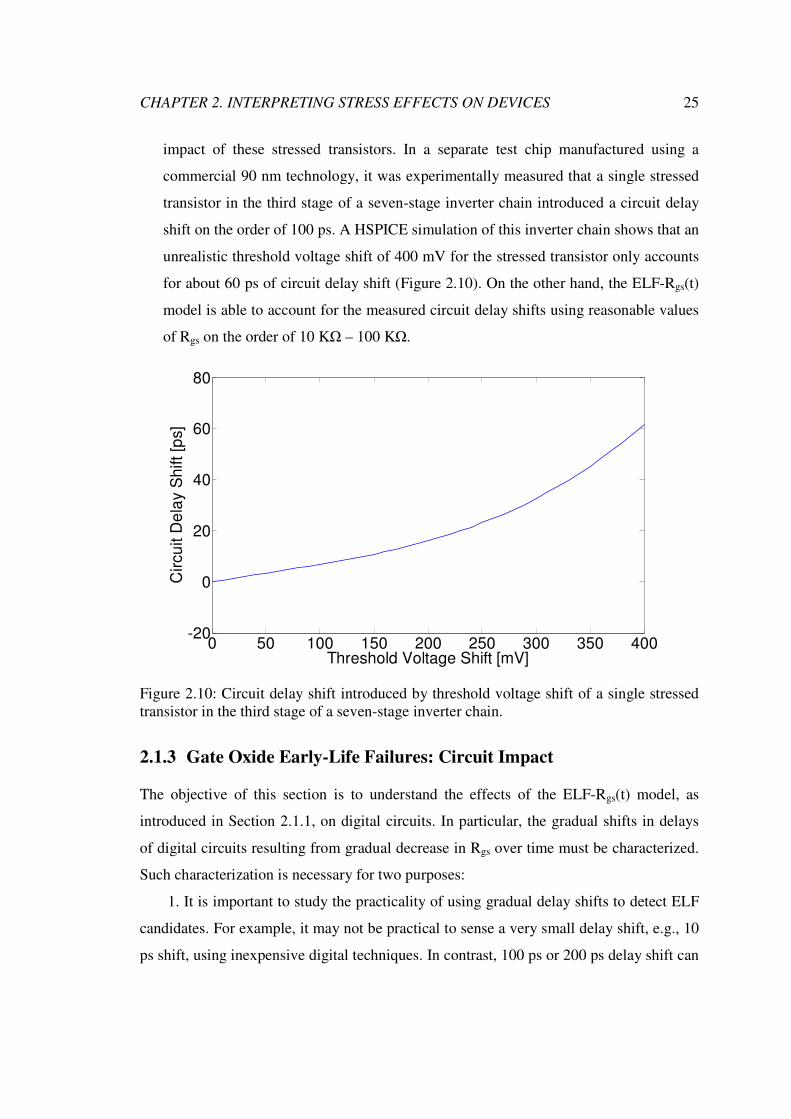
impact of these stressed transistors. In a separate test chip manufactured using a
commercial 90 nm technology, it was experimentally measured that a single stressed
transistor in the third stage of a seven-stage inverter chain introduced a circuit delay
shift on the order of 100 ps. A HSPICE simulation of this inverter chain shows that an
unrealistic threshold voltage shift of 400 mV for the stressed transistor only accounts
for about 60 ps of circuit delay shift (Figure 2.10). On the other hand, the ELF-Rgs(t)
model is able to account for the measured circuit delay shifts using reasonable values
of Rgs on the order of 10 KΩ – 100 KΩ.
0 50 100 150 200 250 300 350 400-20
0
20
40
60
80
Threshold Voltage Shift [mV]
Cir
cu
it D
ela
y S
hift [p
s]
Figure 2.10: Circuit delay shift introduced by threshold voltage shift of a single stressed
transistor in the third stage of a seven-stage inverter chain.
2.1.3 Gate Oxide Early-Life Failures: Circuit Impact
The objective of this section is to understand the effects of the ELF-Rgs(t) model, as
introduced in Section 2.1.1, on digital circuits. In particular, the gradual shifts in delays
of digital circuits resulting from gradual decrease in Rgs over time must be characterized.
Such characterization is necessary for two purposes:
1. It is important to study the practicality of using gradual delay shifts to detect ELF
candidates. For example, it may not be practical to sense a very small delay shift, e.g., 10
ps shift, using inexpensive digital techniques. In contrast, 100 ps or 200 ps delay shift can
Page 48
CHAPTER 2. INTERPRETING STRESS EFFECTS ON DEVICES
26
be practically utilized for ELF prediction using techniques such as stability checkers, e.g.,
[38], or clock control [39, 40].
2. A metric for characterizing the practicality of using gradual delay shifts as an
indicator of ELF is the required Rgs value for a given delay shift, e.g., 100 ps or 200 ps.
The required Rgs value of a transistor for a particular delay shift must be greater than the
Rgsmin value of the corresponding transistor for any technique which uses delay shifts for
ELF prediction.
Detailed SPICE-level simulations on inverter chains using a commercial 90 nm
technology to quantify delay shifts caused by gradual changes in Rgs of the ELF
candidate transistor were performed. Inverter chain simulation using various transistor
sizing scenarios is a standard practice in circuit design. The inverter chain model, shown
in Figure 2.11, contains six inverters. The last inverter acts as the load driven by the
inverter chain. The third inverter contains a gate oxide ELF candidate transistor (PMOS
or NMOS). With six inverters, we can model non-ideal signal transitions at ELF
candidate inverter inputs.
Given an inverter chain with specified inverter sizes, and a delay shift target, the
objective is to identify the Rgs value of the ELF candidate transistor which results in the
desired delay shift. The first simulation setup starts with an inverter chain where every
inverter has a fanout (FO) of 4 (Figure 2.11a). The fanout (FO) of an inverter is defined
as the ratio of its load capacitance (i.e., the input capacitance of the next inverter in the
chain) to its input capacitance. For an FO4 inverter chain, the width of the NMOS
(PMOS) transistor of an inverter is four times larger than that of the NMOS (PMOS)
transistor of the preceding inverter. FO4 inverter chains are commonly used in circuit
design. In our simulation setup, the width of the PMOS transistor of each inverter is twice
that of the corresponding NMOS in order to match pull-up and pull-down inverter delays.
Page 49
CHAPTER 2. INTERPRETING STRESS EFFECTS ON DEVICES
27
Figure 2.11: Six-stage inverter chain. (a) FO4 simulation. (b) Simulation to understand
the effects of transistor sizes.
For this setup, several circuit parameters must be considered:
1. Initial Rgs (time 0) of the ELF candidate transistor: A wide range of initial (time 0)
Rgs values (referred to as Rgsinitial) is swept in order to simulate various degrees of
defective gate oxide of the ELF transistor at time 0.
2. ELF candidate transistor width: For an FO4 inverter chain, Wmin indicates the
width of the NMOS transistor of the first inverter. Hence, the widths of NMOS and
PMOS transistors of the third inverter (with ELF candidate transistors) are 16×Wmin and
32×Wmin, respectively. A range of Wmin values is swept in order to understand the effects
of transistor widths on delay shifts.
3. ELF candidate transistor structure: Transistors with widths that are integer
multiples of Wmin are generally designed using finger structures that connect multiple
transistors with smaller widths in parallel (Figure 2.12). Such structures reduce parasitic
capacitances and the layout area [41]. For an ELF candidate transistor implemented using
a finger structure, an ELF candidate finger is considered; i.e., if a transistor consists of 4
fingers, the gate oxide of the ELF candidate finger may be defective while the remaining
3 fingers may be fine.
4. PMOS vs. NMOS: The width of a PMOS transistor is sized to be twice that of the
corresponding NMOS transistor assuming that PMOS mobility is half of NMOS. This
assumption may not hold at 90 nm technology and beyond – for such technologies PMOS
Page 50
CHAPTER 2. INTERPRETING STRESS EFFECTS ON DEVICES
28
mobility is expected to be greater than half of NMOS. Hence, NMOS and PMOS ELF
candidate transistors are simulated separately to understand their effects on delay shifts.
Figure 2.12: (a) Non-finger gate oxide ELF candidate transistor structure and equivalent
circuit model, (b) 4-finger ELF transistor and equivalent circuit model.
Table 2.1 and Table 2.2 present SPICE simulation results for NMOS and PMOS ELF
candidate transistors in the third inverter of the FO4 inverter chain, respectively. For
example, consider an FO4 inverter chain where the width of the NMOS (ELF candidate)
transistor of the third inverter is 3.2 µm. Note that, this NMOS transistor is implemented
as a finger structure consisting of 4 NMOS transistors of 0.8 µm widths. An arbitrary
finger of this transistor is picked as a gate oxide ELF candidate. As can be seen in Table
2.1, the additional delays introduced at time 0 are very small for Rgsinitial values greater
than 2 KΩ. As a result, these will be very hard to detect using delay testing at time 0. We
also report, Rgsstop, the Rgs value for which the inverter chain stops functioning correctly
(1.7 KΩ for this example). Suppose that a delay shift of 100 ps is to be detected for this
inverter chain. Note that this delay shift is with respect to the delay of the defective
inverter chain at time 0. All Rgs values required for 100 ps, 200 ps or 300 ps delay shifts
are greater than the corresponding Rgsmin values of the fingers. This result confirms that,
for this ELF candidate transistor, gradual delay shifts due to gate oxide early-life failures
Page 51
CHAPTER 2. INTERPRETING STRESS EFFECTS ON DEVICES
29
are practically detectable before hard breakdown of the gate oxide. Note that a delay shift
may or may not cause delay faults depending on timing slacks of circuit paths containing
the ELF candidate transistor. Hence, special techniques (discussed in Section 2.1.4) are
required to sense such delay shifts. In Table 2.1 and Table 2.2, entries with F indicate that
the inverter chain fails to operate correctly at time 0 for very small values of Rgsinitial
resulting in very small transistor drive currents. These severe gate oxide defects can be
detected by testing at time 0.
As Table 2.1 and Table 2.2 demonstrate, when the sizes of all transistors in the FO4
inverter chain are doubled, the required Rgs for a given delay shift becomes roughly half.
This result can be explained using Figure 2.13.
Table 2.1: Rgs for NMOS transistors. Entry with F indicates that the inverter chain fails to
operate correctly at time 0.
ELF candidate width =
3.2 µm
(Width of each finger =
0.8 µm)
ELF candidate width =
6.4 µm
(Width of each finger =
0.8 µm)
ELF candidate width =
12.8 µm
(Width of each finger =
0.8 µm)
Delay shift
(w.r.t. corresp.
time 0 delay)
Delay shift
(w.r.t. corresp.
time 0 delay)
Delay shift
(w.r.t. corresp.
time 0 delay)
Rgsinit
ial (at
time
0)
Time
0
delay
(ps) 100ps 200ps
Time
0
delay
(ps) 100ps 200ps
Time
0
delay
(ps) 100ps 200ps
No
Fault 169.8 N.A. N.A. 170.5 N.A. N.A. 170.9 N.A. N.A.
1 GΩ 169.8 2.46
KΩ
2.05
KΩ 170.5
1.22
KΩ
1.02
KΩ 170.9 0.60KΩ
0.50
KΩ
100
KΩ 170.6
2.45
KΩ
2.05
KΩ 170.9
1.21
KΩ
1.02
KΩ 171.2 0.60KΩ
0.50
KΩ
10 KΩ 179.8 2.38
KΩ
2.03
KΩ 175
1.20
KΩ
1.01
KΩ 173.2 0.60KΩ
0.50
KΩ
9 KΩ 181.1 2.37
KΩ
2.03
KΩ 175.6
1.20
KΩ
1.01
KΩ 173.4 0.60KΩ
0.50
KΩ
8 KΩ 182.8 2.36
KΩ
2.03
KΩ 176.3
1.19
KΩ
1.01
KΩ 173.7 0.60KΩ
0.50
KΩ
4 KΩ 204.7 2.25
KΩ 2KΩ 183.4
1.17
KΩ 1KΩ 176.8 0.60KΩ
0.50
KΩ
2 KΩ 401.1 1.90
KΩ
1.85
KΩ 204.8
1.11
KΩ
0.99
KΩ 183.8 0.58KΩ
0.50
KΩ
1.5KΩ F N.A. N.A. 229.5 1.07
KΩ
0.97
KΩ 189.6 0.57KΩ
0.49
KΩ
Rgssto
p 1.7 KΩ 850 Ω 350 Ω
Rgsmin 243 Ω
Page 52
CHAPTER 2. INTERPRETING STRESS EFFECTS ON DEVICES
30
Table 2.2: Rgs for PMOS transistors. Entry with F indicates that the inverter chain fails to
operate correctly at time 0.
ELF candidate width =
6.4 µm
(Width of each finger =
0.8 µm)
ELF candidate width =
12.8 µm
(Width of each finger =
0.8 µm)
ELF candidate width =
25.6 µm
(Width of each finger =
0.8 µm)
Delay shift
(w.r.t. corresp.
time 0 delay)
Delay shift
(w.r.t. corresp.
time 0 delay)
Delay shift
(w.r.t. corresp.
time 0 delay)
Rgsinit
ial (at
time 0)
Time
0
delay
(ps) 100ps 200ps
Time
0
delay
(ps) 100ps 200ps
Time
0
delay
(ps) 100ps 200ps
No
Fault 188.7 N.A. N.A. 187 N.A. N.A. 185.8 N.A. N.A.
1 GΩ 188.7 1.74
KΩ
1.46
KΩ 187
0.89
KΩ
0.75
KΩ 185.8 0.45KΩ
0.38
KΩ
100
KΩ 189.4
1.74
KΩ
1.46
KΩ 187.4
0.89
KΩ
0.75
KΩ 185.9 0.45KΩ
0.38
KΩ
10 KΩ 196.2 1.70
KΩ
1.45
KΩ 190.7
0.88
KΩ
0.75
KΩ 187.5 0.45KΩ
0.38
KΩ
9 KΩ 197.2 1.70
KΩ
1.45
KΩ 191.1
0.88
KΩ
0.75
KΩ 187.7 0.45KΩ
0.38
KΩ
8 KΩ 198.3 1.69
KΩ
1.45
KΩ 191.7
0.88
KΩ
0.75
KΩ 188 0.45KΩ
0.38
KΩ
4 KΩ 211.1 1.64
KΩ
1.43
KΩ 197
0.87
KΩ
0.74
KΩ 190.4 0.45KΩ
0.38
KΩ
2 KΩ 258.8 1.51
KΩ
1.39
KΩ 210.1
0.84
KΩ
0.74
KΩ 195.7 0.44KΩ
0.38
KΩ
1.5KΩ 363.6 1.39
KΩ
1.34
KΩ 221.9
0.82
KΩ
0.73
KΩ 199.7 0.43KΩ
0.38
KΩ
Rgssto
p 1.2 KΩ 600 Ω 300 Ω
Rgsmin 243 Ω
Page 53
CHAPTER 2. INTERPRETING STRESS EFFECTS ON DEVICES
31
Figure 2.13: (a) 2nd and 3rd stages of FO4 inverter chain of Figure 2.11a. (b) Equivalent
circuit when M2 is on.
Consider the ELF candidate NMOS transistor M3 in the third inverter of the inverter
chain. Figure 2.13b shows the equivalent circuit when the input of the second inverter is
low. It is assumed that Rgate is small compared to Rgs. When all transistor sizes are
doubled, the on-resistance of M3 decreases but the load capacitance also doubles.
However, Vgs of M3 can be expressed as gson
gsdd
RR
RV
+
×
, where Ron is the on-resistance of M2.
As Ron decreases (when the width of M2 is doubled), Rgs must also decrease
proportionally in order to keep Vgs constant (which determines M3 drive current and
delay shift).
As shown in Figure 2.11b, detailed SPICE simulations were performed in order to
understand the sensitivities of Rgs values required for specific delay shifts to circuit
sizing. Not surprisingly, the sizes of the second, third and fourth inverters have the most
prominent effects on Rgs values of ELF candidate transistors in the third inverter. For this
simulation setup, the width of the third inverter in the inverter chain of Figure 2.11b was
fixed to be 1.6 µm, 3.2 µm and 6.4 µm. For each of these cases, the fanouts of the
remaining inverters were varied over three values: 1, 2 and 4, and SPICE simulations
were performed to generate tables similar to Table 2.1 and Table 2.2 (total of 35 SPICE
Page 54
CHAPTER 2. INTERPRETING STRESS EFFECTS ON DEVICES
32
simulations for each transistor type, each initial Rgs value and each delay shift value). The
FO of the last inverter is fixed to 4. The main results from these simulations are
summarized in Table 2.3.
In Table 2.3, the case when the size of the second inverter increases while keeping
the sizes of third and fourth inverters constant is similar to the situation in Figure 2.13.
When the third inverter size increases and other sizes remain constant, the Rgs value for a
specified delay shift decreases because the drive current of the ELF candidate transistor
increases. When the fourth inverter size increases and the other inverter sizes are fixed,
the load capacitance of the ELF candidate transistor increases. Hence, a higher value of
Rgs creates the specified delay shift (making it easier to detect the ELF candidate).
Situations corresponding to the last three rows of Table 2.3 are tricky because the overall
effect depends on the relative importance of the increase in sizes of multiple transistors.
Table 2.3: Sensitivity of Rgs of ELF candidate transistor in third inverter (Figure 2.11b)
for a specified delay chain.
2nd inverter size 3rd (ELF) inverter
size
4th inverter size
Rgs value for a specified delay shift
Increases Constant Constant Decreases Constant Increases Constant Decreases Increases Increases Constant Decreases Constant Constant Increases Increases
Increases Constant Increases Decreases Constant Increases Increases Increases Increases Increases Increases Decreases
2.1.4 ELF Prediction Applications and Related Work
Several earlier publications focused on developing effective ways of identifying early-life
failure candidates. These include several flavors of burn-in and high voltage stress
testing, e.g., [42, 43], Iddq testing and its variants (e.g., [44, 45, 46, 47, 48, 49, 50] and
numerous others), Very Low Voltage (VLV) and minVdd testing [51, 52, 53, 54], outlier
analysis techniques [55, 56, 57, 58, 59], and delay testing techniques for reliability [35,
60, 40, 61]. Major challenges with these techniques include the problem of overkill
(yield-loss) and ways of coping with circuit leakage and process variations. The gradual
Page 55
CHAPTER 2. INTERPRETING STRESS EFFECTS ON DEVICES
33
evolution of Rgs(t) of an ELF candidate transistor, resulting in gradual shifts in delays of
digital circuit paths over time, may be practically used in various ways. A few examples
are outlined.
1. Alternative ELF screening approaches: By observing delay shifts of the circuit
under test, it is possible to reduce dependence on traditional reliability screening. For
example, one approach is to detect delay shifts of circuits under test after a short high
voltage stress. Unlike traditional high-voltage stress or delay testing approaches for gate
oxide shorts, the idea here is to detect relative delay shifts (e.g., 100 ps in Section 2.1.3)
even if the chip passes testing after stress. The amount of delay shift to be detected must
be properly chosen to eliminate the effects of circuit aging such as Negative Bias
Temperature Instability (NBTI). Since we are targeting early-life failures that are relevant
typically within a few weeks to months from production, aging effects are not expected to
induce large delay shifts of 100 ps over that period of time. Unlike parametric
measurements suggested in [62], test support for faster than at-speed testing [39, 40] can
be useful for identifying such delay shifts. However, unlike traditional faster-than-rated-
speed delay test techniques, the delay shift technique has minimal sensitivity to process
variations, noise and overkill (yield-loss) problems. This is because the delay shift
technique relies on “relative” measurements of delays of the same circuit over time. Such
a delay shift technique can also significantly benefit from existing outlier analysis
techniques. Large-scale ELF experiments are required to validate these observations.
2. On-line circuit failure prediction: The idea behind circuit failure prediction [38]
is to predict the occurrence of a failure during normal system operation before the
appearance of any error that can result in corrupt system data and states. This is in
contrast to classical error detection where a failure is detected after errors appear in
system data and states. Since gate oxide ELF candidates result in the gradual delay shifts
of digital circuits, it may be possible to adapt circuit failure prediction (e.g., [38])
together with on-line self-test for ELF prediction during system operation.
3. Adaptive testing and reliability screening: Delay shifts from high-voltage stress
testing may be used to identify possibly-weak chips that need to undergo very thorough
testing and reliability screening. Such an adaptive approach can help reduce the overall
cost of test and reliability screening.
Page 56
CHAPTER 2. INTERPRETING STRESS EFFECTS ON DEVICES
34
2.2 Using Post-Breakdown Device-Level Behavior to
Model ESD Effects
ESD-related damages make up a third of all field returns, and providing sufficient ESD
protection is essential for keeping product yield high. In addition, gate oxide thickness for
high-performance transistors in state-of-the art bulk CMOS technology is approaching 1
nm due to aggressive scaling. Having such a thin gate oxide means that gate oxides are
much more vulnerable to gate oxide breakdowns than in past technology nodes. The use
of high-K dielectrics gives a one-time gain in oxide thickness, but is not expected to solve
the fundamental problem of thin gate oxides in advanced CMOS technologies. Therefore,
a physics-based methodology for designing chips that are robust to ESD events is
necessary.
This section looks at the behavior of devices broken down by ESD events. It was
found that transistors exhibit a stable resistance after hard breakdown, and that this
resistance has a power-law relationship with oxide area. This information enables the
development of a physics-based post-breakdown transistor macro-model, as to be
discussed in Chapter 3.
2.2.1 Emulating ESD Stress
90 nm and 130 nm N and P devices were studied in this work. For 130 nm devices, oxide
thickness is 2.2 nm for thin oxide devices and 6.2 nm for thick oxide devices. For 90 nm
devices, oxide thickness is 1.6 nm for thin oxide devices. The channel lengths vary from
minimum channel length to 10 µm. The device widths vary from 0.15 µm to 10 µm.
Two different stress procedures were used in this study. For the first set of
devices, a 740 ps pulse generated from a Very-Fast Transmission Line Pulsing system
(VFTLP) constructed based on [63, 64] was applied to the Gate with the Source, Drain,
and Substrate grounded, until hard breakdown occurred. After each pulse, leakage
resistance is measured using 0.1 V DC at the Gate. This low voltage of 0.1 V DC is used
in order to avoid further oxide damage. Hard breakdown is defined in this study as a low
leakage resistance which remains constant with further stress. Gate capacitors with
Page 57
CHAPTER 2. INTERPRETING STRESS EFFECTS ON DEVICES
35
Source, Drain and Substrate shorted internally were used in this study to reduce parasitic
effects.
For the second set of devices, a 0 to +/-5 V ramp was applied to the Gate with the
Source, Drain and Substrate grounded. These devices were stressed until hard breakdown
as defined previously. To prevent burn-out of interconnects and/or contacts, current
compliance is set according to device size. Current compliance is always at least 3 mA
for all devices. Figure 2.14 shows the experimental setup.
Figure 2.14: Schematic of experimental setup. A NMOS example is shown. The Stress
Voltage is a 740 ps pulse for the first set of devices, and a 0 to +/-5 V ramp for the second
set of devices.
2.2.2 Post-breakdown Device Behavior
Both sets of devices were broken down as previously described, and leakage resistance
was measured. As can be seen from Figure 2.15, the measured post-breakdown V/I value
remains approximately constant from 0-1 V, which indicates a resistor-like behavior at
low voltages.
N+
P Substrate
+
_
Stress
Voltage
N+
Gate
Page 58
CHAPTER 2. INTERPRETING STRESS EFFECTS ON DEVICES
36
0 0.2 0.4 0.6 0.8 10
500
1000
1500
2000
2500
3000
Voltage [V]
Re
sis
tan
ce
[Ω
]
130nm Sample 1130nm Sample 2130nm Sample 3130nm Sample 490nm W/L=10/0.0990nm W/L=10/0.1890nm W/L=10/2.490nm W/L=10/10
Figure 2.15: Typical post-breakdown leakage resistance as a function of Voltage for 90
nm and 130 nm N thin oxide devices. 130 nm devices have W/L=20/0.115, while 90 nm
devices have W/L as specified on figure. The resistance is almost constant from 0-1 V for
all devices shown.
2.2.2.1 Pulse Stress
Figure 2.16 and Figure 2.17 show the leakage resistance measured after the third pulse
for 130 nm N and P thick and thin oxide capacitors in accordance with the Joint Electron
Device Engineering Council (JEDEC) standard for CDM testing [65]. W/L is 10 µm /10
µm for these devices. It can be seen that there is a characteristic post-breakdown leakage
resistance floor on the order of 100 Ω for all the devices.
Page 59
CHAPTER 2. INTERPRETING STRESS EFFECTS ON DEVICES
37
17 17.5 18 18.5 19 19.510
0
102
104
106
108
1010
Voltage [V]
Re
sis
tan
ce
[Ω
]
130nm N Thin Oxide130nm P Thin Oxide
Post Breakdown Leakage Resistance Floor
Figure 2.16: Figure showing leakage resistance after the third pulse as a function of
Voltage across the Gate with the Source, Drain and Substrate grounded for 130 nm N and
P thin oxide devices. A post-breakdown leakage resistance floor of about 100 Ω is noted.
Page 60
CHAPTER 2. INTERPRETING STRESS EFFECTS ON DEVICES
38
48 50 52 54 56 58 60 6210
1
102
103
104
105
106
107
Voltage [V]
Re
sis
tan
ce
[Ω
]
130nm N Thick Oxide130nm P Thick Oxide
Post Breakdown Leakage Resistance Floor
Figure 2.17: Figure showing leakage resistance after the third pulse as a function of
Voltage across the Gate for 130 nm N and P thick oxide devices. It may be seen that there
is a resistance floor of ~100 Ω after hard breakdown even with further stress.
2.2.2.2 Ramp Stress
To correlate the data presented above with those obtained from a ramp stress, a 0 to 5
V ramp was applied to the N type thin oxide device until breakdown occurred. As can be
seen from Table 2.4, it was observed that both stress procedures resulted in similar post-
breakdown leakage resistance.
Table 2.4: Table summarizing the post-breakdown leakage resistance of 130 nm N Thin
Oxide capacitor after different stress conditions. It can be seen that different stress
conditions resulted in similar post-breakdown leakage resistance.
Stress Type Mean R [Ω] Std. Dev. [Ω]
740 ps pulse 95.1 19.7
Ramp 99.6 5.8
Page 61
CHAPTER 2. INTERPRETING STRESS EFFECTS ON DEVICES
39
Both 90 nm and 130 nm N and P thin oxide devices with varying widths and
lengths were stressed in both accumulation and inversion using a 0 to +/-5 V ramp. It
may be seen from Figure 2.18 and Figure 2.19 that there is a linear relation, on a log-log
plot, between the post-breakdown leakage conductance and device area for both N and P
type devices, under inversion or accumulation stress.
-14 -13.5 -13 -12.5 -12 -11.5 -11 -10.5-6.5
-6
-5.5
-5
-4.5
-4
-3.5
-3
-2.5
-2
-1.5
log(Area) [log(m2)]
log
(1/R
es
ista
nc
e)
[lo
g(1
/Ω
)]
90nm N Thin Oxide Accumulation measurements
Linear fit
90nm N Thin Oxide Inversion measurements
Linear fit
Figure 2.18: Figure showing the linear relationship in a log-log plot between the inverse
of post-breakdown leakage resistance and device area for 90 nm N thin oxide devices.
Page 62
CHAPTER 2. INTERPRETING STRESS EFFECTS ON DEVICES
40
-13.5 -13 -12.5 -12 -11.5 -11 -10.5-7.5
-7
-6.5
-6
-5.5
-5
-4.5
-4
-3.5
-3
-2.5
-2
log(Area) [log(m2)]
log
(1/R
es
ista
nc
e)
[lo
g(1
/Ω
)]
90nm P Thin Oxide Accumulation measurements
Linear fit
90nm P Thin Oxide Inversion measurements
Linear fit
Figure 2.19: Figure showing the linear relationship in a log-log plot between the post-
breakdown leakage conductance and device area for 90 nm P thin oxide devices.
2.2.3 Understanding Post-breakdown Device-level Behavior
Measurements show that post-breakdown leakage resistance is a function of device area.
This indicates that successive breakdown has occurred, resulting in multiple breakdown
paths [66]. As such, the total number of breakdown paths is expected to be a function of
device area.
On a log-log plot, a gradient of 1 indicates a linear relationship between X-Y axes.
For the linear fits in Figure 2.18 and Figure 2.19, the gradients are about 0.7. The fact that
the gradients are close to, but not exactly, 1 is expected because of secondary W and L
effects on the post-breakdown leakage resistance. This is because carriers traveling
through breakdown paths directly over the Source and Drain regions are collected more
efficiently than carriers traveling through breakdown paths from Gate to Substrate [67].
Page 63
CHAPTER 2. INTERPRETING STRESS EFFECTS ON DEVICES
41
Data also shows that NMOS in inversion exhibits the hardest breakdown, which is
consistent with the findings of other authors [68]. This is because electron transport is the
dominant charge transport mechanism during stress, and is also the dominant conduction
mechanism during the first stage of breakdown discharge. Hardening breakdown spots
require a good supply and a good drain for electrons [69]. Therefore, an NMOS stressed
in inversion exhibits the hardest breakdown because of the availability of electrons in
Source and Drain regions, and the low resistance path of the n+-polysilicon anode [68].
In addition, data shows that the post-breakdown leakage resistance is similar for both
thick (6.2 nm) and thin (2.2 nm) oxide devices fabricated in 130 nm technology. This
suggests that the resistance of the breakdown path through the oxide is thickness-
independent. This result agrees well with the work of other authors who suggested that
there is little or no voltage drop in the oxide path [70, 71].
2.3 Chapter Summary
This chapter looked at the behavior of both pre- and post-breakdown devices, and how
their defining characteristics may be used to design robust systems.
Pre-breakdown devices have well-defined cut-off, linear, and saturation regions of
operations. The defining characteristic of pre-breakdown devices is that the drive current
degrades gradually with stress, until it abruptly loses all transistor characteristics and
behaviors like a resistor. The gradual degradation of drive current translates into an
increase in the delay of a digital circuit containing the stressed, pre-breakdown transistor
before functional failure occurs. Detailed simulations have been performed to show that
such delay increases are significant enough for inexpensive digital techniques to reliably
detect that a transistor is undergoing degradation, and predict circuit failure before
functional failure actually occurs. Appropriate actions may then be taken so that the user
does not see any downtime or recovery efforts.
Post-breakdown devices have a stable resistance which does not change with
increased stress. It was also experimentally shown that devices broken down by either
pulse stresses or ramp stresses exhibit similar post-breakdown leakage resistance. Post-
breakdown leakage resistance has a power-law relationship with oxide area, indicating
Page 64
CHAPTER 2. INTERPRETING STRESS EFFECTS ON DEVICES
42
multiple breakdown locations. The stable post-breakdown leakage resistance enables the
development of a physics-based post-breakdown transistor macro-model, as to be
discussed in Chapter 3.
Page 65
43
Chapter 3
Post-breakdown Transistor Macro-
Model for 90 nm and 130 nm
Technologies
A physics-based design methodology for robust system design requires a scalable post-
breakdown transistor macro-model. This is because gate oxide breakdown does not
necessarily imply function failure; the location of the breakdown within the circuit is also
important. This macro-model must also be scalable, in order for it to be implemented in a
design tool to aid designers of reliable chips. This tool can then be used to predict if gate
oxide breakdowns in certain locations will cause chip level functional failure, as will be
discussed in Chapter 5. Protection strategies for preventing these critical transistors from
breaking down in the first place can then be designed-in.
This chapter presents a unified macro-model for post-breakdown transistors that
integrates all observed ESD-CDM effects, and is experimentally verified in 90 nm and
130 nm CMOS technologies. Section 3.1 presents the macro-model, and Section 3.2
presents the experimental verification. This macro-model enables a physics-based
approach to reliable circuit design. Designers will be able to extract circuit-specific
netlists from physical layouts, and determine if reliability threats affect the robustness of
their systems.
Page 66
CHAPTER 3. POST-BREAKDOWN TRANSISTOR MACRO-MODEL FOR
90 NM AND 130 NM TECHNOLOGIES
44
3.1 Post-breakdown Transistor Macro-Model
Additional current leakage paths are formed through the gate oxide when breakdowns
happen. However, it has also been reported that intrinsic MOSFET parameters such as
transconductance (gm) are degraded after gate oxide breakdown [72]. This degradation is
observed to be a function of device width and is particularly significant in narrow-width
transistors (width < 1 µm). Therefore, it is not sufficient, nor is it physical, to simply
model the additional resistive leakage paths when modeling post-breakdown transistors.
130 nm and 90 nm transistors are broken down, as described in Section 3.1.1, in order to
study the behavior of post-breakdown transistors.
3.1.1 Experiments
In order to develop an accurate, scalable macro-model for post-breakdown transistors, Ids-
Vds characteristics of 90 nm and 130 nm of post-breakdown NMOS transistors were
studied in this section.
Oxide thickness for 90 nm transistors is 1.6 nm, and oxide thickness for 130 nm
transistors is 2.2 nm. The channel lengths vary from minimum channel length to 10 µm.
The device widths vary from 0.15 µm to 20 µm. A 0 to 5 V ramp stress was applied to the
Gate, with Source, Drain and Substrate grounded. The stress was applied until hard
breakdown, defined as a low resistance that remains constant with further stress.
Transistor Ids-Vds characteristics were then recorded. As discussed in Chapter 2, this
ramp-stress procedure results in a breakdown state similar to the breakdown state caused
by a 740 ps pulse applied to the Gate with Source, Drain and Substrate grounded.
The advantage of using the ramp-stress procedure for this study is that four-terminal
transistors may be used, and post-breakdown Ids-Vds characteristics can be readily
measured. Otherwise, if 740 ps stress pulses are to be used, the test devices must be two-
terminal gate capacitors. This is because parasitic effects of four-terminal devices prevent
the application of well-controlled fast transient pulses on the gate. Post-breakdown Ids-Vds
characteristics then cannot be easily measured as Source, Drain and Substrate are shorted
due to RF considerations.
Page 67
CHAPTER 3. POST-BREAKDOWN TRANSISTOR MACRO-MODEL FOR
90 NM AND 130 NM TECHNOLOGIES
45
3.1.2 Macro-Model
It has been reported that hard breakdown results in a unique state for the transistor [73].
A macro-model for post-breakdown transistors with multiple breakdown paths is shown
in Figure 3.1 with all parameters summarized in Table 1. In this model, Rleak is the
device oxide area-dependent post-breakdown leakage resistance as shown in [73], and
Lfresh and Wfresh is the length and width of the fresh device respectively. The physical
origins for the elements in this model are discussed in [67]. While the initial model
proposed in [67] captures essential physics, both in device-level simulations and based on
experiments, several key geometry and scaling effects are essential to make the model
useful for design applications. Namely, geometry effects in the devices as well as suitable
scaling of the resistors need to be considered more carefully.
The model proposed in this work accounts for intrinsic transistor degradation, is
valid for multiple breakdown events, and enables a systematic approach for evaluating all
elements used in the model given transistor geometries and without requiring fitting
parameters. These properties are essential for this macro-model to be implemented in a
circuit design tool; if the macro-model were not scalable, different fitting parameters
would have to be obtained for all transistor geometries used, which is certainly
unfeasible.
In the macro-model as shown in Figure 3.1, Rgate accounts for series gate resistance.
Rleak is defined in [73] and Chapter 2 as post-breakdown leakage resistance measured
with 0.1 V at the Gate. Since 0.1 V is below threshold and none of the transistors in the
model are turned on, only Gate-to-Source (Rgs) and Gate-to-Drain resistance (Rgd) are in
parallel. Rgs and Rgd are assumed to be symmetric because both Source and Drain
terminals are grounded during stress, and there is no distinction between the Source and
Drain terminals. Thus, Rgs and Rgd each has a resistance of 2*Rleak.
RgsMOS, RgdMOS, MgsMOS and MgdMOS model the leakage paths from Gate to
Source and Drain through the Channel. Channel leakage paths are physically transistors
with very short channel lengths, which are modeled by MgsMOS and MgdMOS.
Essentially, transistor action means that carriers are injected from the Source into the
Drain through the inversion layer. With resistive breakdown paths connecting the
inversion layer and the poly-silicon gate, the poly-silicon gate acts as an additional sink
Page 68
CHAPTER 3. POST-BREAKDOWN TRANSISTOR MACRO-MODEL FOR
90 NM AND 130 NM TECHNOLOGIES
46
for carriers traveling in the inversion layer. This is the physical origin of MgsMOS and
MgdMOS. These leakage paths will be dominated by direct Gate-to-Source and Gate-to-
Drain breakdown paths in wide devices due to the carrier collection efficiency of highly-
doped Source and Drain regions. To model this effect, RgsMOS and RgdMOS are defined
as (Wfresh/1 µm)*Rleak. MgsMOS and MgdMOS model the transistors formed by Gate-
Source and Gate-Drain regions after breakdown [67]. As shown in [73], this high voltage,
sub-nanosecond pulse causes multiple breakdown paths. Since successive breakdown
paths are not spatially correlated [74], the average effective length of MgsMOS and
MgdMOS is 0.5*Lfresh, as shown in Figure 3.2. Multiple breakdowns mean both MgsMOS
and MgdMOS will span Wfresh. However, since MgsMOS and MgdMOS are in parallel, the
effective width of MgsMOS and MgdMOS is 0.5*Wfresh.
To account for post-breakdown degradation of the intrinsic transistor, the effective width
after breakdown is modeled as W=Wfresh*(1-0.35 µm /Wfresh). The value 0.35 µm is
deduced from the analysis in [72], and also correlates well with experimental data. The
resulting degradation of intrinsic transistor parameters is comparable with experimental
data reported in [72].
Figure 3.1: Figure showing the complete post-breakdown transistor macro-model. This
model is valid for both 130 nm and 90 nm technologies.
MgsMOS MgdMOS
Rgate
Rgd
Drain Source
RgsMOS RgdMOS
Gate
Degraded Intrinsic MOS
Rgs
Page 69
CHAPTER 3. POST-BREAKDOWN TRANSISTOR MACRO-MODEL FOR
90 NM AND 130 NM TECHNOLOGIES
47
Table 3.1: Table summarizing the modeling methodology for the elements in Figure 3.1.
Element Value
Rgs, Rgd 2*Rleak
RgdMOS,
RgsMOS
(Wfresh/1 µm)*Rleak
MgsMOS, MgdMOS W=0.5*Wfresh
L=0.5*Lfresh
Degraded Intrinsic
MOS
W=Wfresh*
(1-0.35 µm /Wfresh)
L=Lfresh
Figure 3.2: This figure shows the top-view of device Oxide area with Source at the top
and Drain at the bottom. The numbered circles represent breakdown locations. Each
breakdown location will form an MgsMOS and MgdMOS, each with its own Leffective.
Since breakdown locations are spatially uncorrelated, the aggregate Leffective for all
MgsMOS and MgdMOS is Lfresh/2. Since multiple MgsMOS and MgdMOS will span Wfresh,
the aggregate effective width for MgsMOS and MgdMOS is Wfresh/2, as discussed in
Section 3.1.2.
Drain
Source
Drain
Gate
Enlarged view of Gate area
Leffective
MgsMOS
2 Leffective
MgsMOS
2
Source
Leffective
MgdMOS
1
Leffective
MgsMOS
1
1
2
Oxide
Leffective
MgsMOS
3 3
Leffective
MgdMOS
3
Weffective
MgsMOS
Weffective
MgsMOS
2
Weffective
MgsMOS
3
Weffective
MgdMOS
Weffective
MgdMOS
2
Weffective
MgdMOS
3
Lfresh
Wfresh
Page 70
CHAPTER 3. POST-BREAKDOWN TRANSISTOR MACRO-MODEL FOR
90 NM AND 130 NM TECHNOLOGIES
48
3.2 Experimental Verification of Macro-Model
This section presents experimental verification of the post-breakdown transistor macro-
model presented in the previous section. Section 3.2.1 presents experimental verification
of the model in 130 nm CMOS technology, and Section 3.2.2 verifies the model in 90 nm
CMOS technology. The macro-model presented in Section 3.1.2 is shown to be scalable,
as simulated Ids-Vds characteristics of post-breakdown transistors match experimental
observations for a wide range of geometries. This feature of the macro-model is essential
for enabling a physics-based design methodology for robust digital systems as discussed.
3.2.1 Verification for 130 nm CMOS Technology
Figure 3.3 shows the macro-modeling results for a post-breakdown 130 nm device with
W/L=20 µm / 2.4 µm. Experimental data is compared against the macro-model. Fresh
transistor Ids-Vds characteristics are shown for comparison.
0 0.5 1 1.5-1.5
-1
-0.5
0
0.5
1
1.5
2x 10
-3
Vds
[V]
I ds [
A]
Fresh Device
Vgs
= 1.2V
Vgs
= 0.6V
Vgs
= 0V
(a)
Page 71
CHAPTER 3. POST-BREAKDOWN TRANSISTOR MACRO-MODEL FOR
90 NM AND 130 NM TECHNOLOGIES
49
0 0.5 1 1.5-1.5
-1
-0.5
0
0.5
1
1.5
2x 10
-3
Vds
[V]
I d [
A]
Experimental dataMacro model
Vgs
= 0V
Vgs
= 1.2V
Vgs
= 0.6V
Figure 3.3: Figure showing macro-model modeling post-breakdown transistor
characteristics. (a) Fresh device characteristics. (b) Macro-model results compared with
measurements. (c) Macro-model used for this simulation. The same scale is used for both
Ids-Vds curves in (a) and (b) for comparison. Device shown is 130 nm with W/L=20 µm /
2.4 µm. The macro-model correlates well with measured post-breakdown characteristics
even though post-breakdown device characteristics are significantly different from fresh
device characteristics.
Drain Source
Gate
(b)
(c)
Page 72
CHAPTER 3. POST-BREAKDOWN TRANSISTOR MACRO-MODEL FOR
90 NM AND 130 NM TECHNOLOGIES
50
The macro-model discussed up to this point has assumed symmetry between Source
and Drain. This macro-model can be further validated by breaking the Source-Drain
symmetry. By shorting Drain to Gate when stressing the device, there will be no voltage
drop across the oxide in the Gate-Drain overlap region. As such, breakdown in the Gate-
Drain overlap region will be minimized i.e., there is no Rgd. Figure 3.4 shows the
comparison between the modified macro-model without Rgd and experimental data for a
130 nm device with W/L=20 µm / 0.115 µm stressed with Drain shorted to Gate as
described above.
0 0.5 1 1.5-5
0
5
10
15x 10
-3
Vds
[V]
I ds [
A]
Fresh Device
Vgs
= 1.2V
Vgs
= 0.6V
Vgs
= 0V
(a)
Page 73
CHAPTER 3. POST-BREAKDOWN TRANSISTOR MACRO-MODEL FOR
90 NM AND 130 NM TECHNOLOGIES
51
0 0.5 1 1.5-5
0
5
10
15x 10
-3
Vds
[V]
I d [
A]
Experimental dataMacro model
Vgs
= 1.2V
Vgs
= 0.6V
Vgs
= 0V
Figure 3.4: Figure showing macro-model results for transistors with no direct Gate-to-
Drain breakdown paths. (a) Fresh device characteristics. (b) Macro-model results
compared with measurements. (c) Macro-model used for this simulation. Device shown
is 130 nm with W/L=20 µm / 0.115 µm. Macro-model matches measured data even if
post-breakdown device is asymmetrical.
Gate
Drain Source
(b)
(c)
Page 74
CHAPTER 3. POST-BREAKDOWN TRANSISTOR MACRO-MODEL FOR
90 NM AND 130 NM TECHNOLOGIES
52
0 0.5 1 1.5-5
0
5
10
15x 10
-3
Vds
[V]
I d [
A]
Experimental dataMacro model
Vgs
= 1.2V
Vgs
= 0.6V
Vgs
= 0V
Figure 3.5: Figure showing macro-model results for transistors with no direct Gate-to-
Source breakdown paths. (a) Macro-model results compared with measurements. (b)
Macro-model used for this simulation. Fresh device characteristics are the same as Figure
3.4. The same scale is used for both Ids-Vds curves in Figure 3.4 and Figure 3.5 for
comparison. The same device used for Figure 3.4 is used here, with the Source and Drain
terminals switched. The macro-model fits measured data. Together with Figure 3.4, this
result validates the macro-model for 130 nm technology.
Gate
Source Drain
(a)
(b)
Page 75
CHAPTER 3. POST-BREAKDOWN TRANSISTOR MACRO-MODEL FOR
90 NM AND 130 NM TECHNOLOGIES
53
Furthermore, due to the asymmetry of this breakdown mode, different Ids-Vds
characteristics are expected when the terminal with no direct breakdown paths is shorted
to Ground (used as Source for NMOS) and the terminal with direct breakdown paths is
swept from 0 to Vdd (used as Drain for NMOS). Figure 3.5 shows the comparison
between the macro-model and experimental data. The same device is shown in Figure 3.4
and Figure 3.5, except that the Source and Drain terminals are switched as described.
3.2.2 Verification for 90 nm CMOS Technology
The same technique is used to verify the model for 90 nm devices. First, a symmetric
macro-model will be shown to match experimental data. Next, another device will be
broken down asymmetrically, and be shown to match experimental data as well. Finally,
a device with no direct Gate-to-Source and Gate-to-Drain breakdown paths will be
presented. This type of breakdown is used to validate the modeling of the channel
leakage paths and the degradation of the intrinsic MOS.
Figure 3.6 compares the macro-model against experimental data for a 90 nm device
with W/L=2 µm / 0.1 µm, broken down symmetrically.
0 0.5 1 1.5-1
-0.5
0
0.5
1
1.5
2
2.5
3x 10
-3
Vds
[V]
I ds [
A]
Fresh Device
Vgs
= 1.2V
Vgs
= 0.6V
Vgs
= 0V
(a)
Page 76
CHAPTER 3. POST-BREAKDOWN TRANSISTOR MACRO-MODEL FOR
90 NM AND 130 NM TECHNOLOGIES
54
0 0.5 1 1.5-1
0
1
2
3x 10
-3
Vds
[V]
I d [
A]
Experimental dataMacro model
Vgs
= 1.2V
Vgs
= 0.6V
Vgs
= 0V
Figure 3.6: Figure showing macro-model modeling post-breakdown transistor
characteristics. (a) Fresh device characteristics. (b) Macro-model results compared with
measurements. (c) Macro-model used for this simulation. The same scale is used for both
Ids-Vds curves for comparison. 90 nm device with W/L=2 µm / 0.1 µm is shown. Macro-
model matches measured post-breakdown characteristics even though fresh device
characteristics are very different.
Drain Source
Gate
(b)
(c)
Page 77
CHAPTER 3. POST-BREAKDOWN TRANSISTOR MACRO-MODEL FOR
90 NM AND 130 NM TECHNOLOGIES
55
Figure 3.7 and Figure 3.8 shows the same asymmetrically broken down 90 nm
device. In Figure 3.7, the device is broken down in such a way that there are no direct
Gate-to-Drain breakdown paths.
0 0.5 1 1.5-4
-2
0
2
4
6
8
10
12x 10
-3
Vds
[V]
I ds [
A]
Fresh Device
Vgs
= 1.2V
Vgs
= 0.6V
Vgs
= 0V
0 0.5 1 1.5
0
5
10
x 10-3
Vds
[V]
I d [
A]
Experimental dataMacro model
Vgs
= 1.2V
Vgs
= 0.6V
Vgs
= 0V
(b)
(a)
Page 78
CHAPTER 3. POST-BREAKDOWN TRANSISTOR MACRO-MODEL FOR
90 NM AND 130 NM TECHNOLOGIES
56
Figure 3.7: Figure showing macro-model results for transistors with no direct Gate-to-
Drain breakdown paths. (a) Fresh device characteristics. (b) Macro-model results
compared with measurements. (c) Macro-model used for this simulation. 90 nm device
with W/L=10 µm / 0.09 µm is shown. The macro-model is valid even if the device
breakdown is asymmetrical.
In Figure 3.8, the device is broken down in such a way that there are no direct Gate-
to-Source breakdown paths.
0 0.5 1 1.5
0
5
10
x 10-3
Vds
[V]
I d [
A]
Experimental dataMacro model
Vgs
= 1.2V
Vgs
= 0.6V
Vgs
= 0V
Gate
Drain Source (c)
(a)
Page 79
CHAPTER 3. POST-BREAKDOWN TRANSISTOR MACRO-MODEL FOR
90 NM AND 130 NM TECHNOLOGIES
57
Figure 3.8: Figure showing macro-model results for transistors with no direct Gate-to-
Source breakdown paths. (a) Macro-model results compared with measurements. (b)
Macro-model used for this simulation. Fresh device characteristics are the same as Figure
3.7. The same scale is used for both Ids-Vds curves in Figure 3.7 and Figure 3.8 for
comparison. The same device used for Figure 3.7 is used here, with the Source and Drain
terminals switched. The macro-model fits measured data. Together with Figure 3.7, this
result validates the macro-model for 90 nm technology.
Transistors were also stressed so that there are no direct Gate-to-Source and Gate-to-
Drain breakdown paths. Figure 3.9 shows the modified macro-model without Rgd and Rgs,
for a 90 nm device with W/L=0.36 µm / 1 µm. The agreement between macro-modeling
results and experiments shows that the modeling of the breakdown paths through the
Channel (MgsMOS, MgdMOS, RgsMOS, RgdMOS), and the modeling of the Degraded
Intrinsic MOS is realistic. This is because there are no direct breakdown paths (Rgs, Rgd)
that might otherwise dominate the current characteristics in some cases.
Gate
Source Drain (b)
Page 80
CHAPTER 3. POST-BREAKDOWN TRANSISTOR MACRO-MODEL FOR
90 NM AND 130 NM TECHNOLOGIES
58
0 0.5 1 1.5-10
-8
-6
-4
-2
0
2
4
6
x 10-5
Vds
[V]
I ds [
A]
Fresh Device
Vgs
= 1.2V
Vgs
= 0.6V
Vgs
= 0V
0 0.5 1 1.5-10
-5
0
5
x 10-5
Vds
[V]
I d [
A]
Experimental dataMacro model
Vgs
= 1.2V
Vgs
= 0.6V
Vgs
= 0V
(a)
(b)
Page 81
CHAPTER 3. POST-BREAKDOWN TRANSISTOR MACRO-MODEL FOR
90 NM AND 130 NM TECHNOLOGIES
59
Figure 3.9: Figure showing macro-model results for transistors with no direct Gate-to-
Source and Gate-to-Drain breakdown paths. (a) Fresh device characteristics. (b) Macro-
model results compared with measurements. (c) Macro-model used for this simulation.
The same scale is used for both Ids-Vds curves for comparison. 90 nm device with
W/L=0.36 µm / 1 µm shown. This result shows that the macro-model is valid even if Rgs
and Rgd are not present i.e., the modeling of MgsMOS, MgdMOS, RgsMOS, RgdMOS and
Degraded Intrinsic MOS fit measured post-breakdown device characteristics.
3.2.3 Macro-model Verification
The accuracy of this macro-model is verified with 30 transistors of various geometries.
The transistors were broken down as described, and the measured current characteristics
were compared against the predictions of the macro-model. It is shown that the root mean
squared error of this macro-model is 9.64%, with a standard deviation of 3.78% (Table
3.2). This accuracy is reasonable, especially considering that breakdown is a statistical
event.
Table 3.2: Table summarizing macro-model accuracy.
Number of transistors Root mean squared error
[%]
Standard Deviation [%]
30 9.64 3.78
Gate
Drain Source (c)
Page 82
CHAPTER 3. POST-BREAKDOWN TRANSISTOR MACRO-MODEL FOR
90 NM AND 130 NM TECHNOLOGIES
60
3.3 Chapter Summary
A post-breakdown transistor macro-model is presented in this chapter. This physics-
based macro-model unifies effects caused by additional leakage paths as well as effects
caused by the degradation of intrinsic MOSFET parameters. No fitting parameters are
used in this macro-model. This model has been experimentally shown to be valid for
various circuit configurations in both 130 nm and 90 nm CMOS technologies.
This macro-model uses the understanding of post-breakdown device-level behavior
as discussed in Chapter 2, and will be implemented in the physics-based design tool for
robust digital systems design in Chapter 5.
Page 83
61
Chapter 4
Ultra-Fast Transmission Line Pulsing
System
Commercial Transmission Line Pulsing systems (TLP) and Very-Fast Transmission Line
Pulsing systems (VFTLP) are used in industry to simulate ESD-CDM events on the wafer
level. These systems can produce voltage pulses with pulse widths as narrow as 1 ns.
This is because standard bodies such as the Joint Electron Device Engineering Council
(JEDEC) and the Electrostatic Discharge Association (ESDA) specify that ESD-CDM
testing is to be done with 1 ns pulses.
As discussed in Chapter 1, aggressive scaling of gate oxide thickness has caused
devices to be much more vulnerable to ESD events. In particular, induced ESD-CDM
events, which were not reported for technology before 130 nm CMOS, became a real
concern for advanced technologies. Induced ESD-CDM events are very fast transient
pulses, with pulse widths in the 100 ps regime, which can cause gate oxide breakdown of
core devices. Therefore, an Ultra-Fast Transmission Line Pulsing system (UFTLP)
capable of producing sub 100 ps pulses is needed to study device-level effects of induced
ESD-CDM events. Understanding the device-level behavior of transistors under induced
ESD-CDM stress is critical to the development a physics-based design methodology for
digital systems robust to ESD-CDM events, as to be discussed in Chapter 5.
Page 84
CHAPTER 4. ULTRA-FAST TRANSMISSION LINE PULSING SYSTEM
62
This chapter discusses the reasons for commercial VFTLP systems to be limited to
producing pulses in the nanosecond regime. A novel architecture for the UFTLP,
experimentally shown to be capable of producing sub 100 ps pulses, is also presented.
4.1 TLP and VFTLP Systems
Figure 4.1 shows a typical TLP system. It is made up of a transmission line, and a pulse
delivery system which consists of everything else in the TLP system other than the
transmission line and the high voltage source. There are two modes of operation:
Charging and Discharging. During Charging, the transmission line is connected to a high
voltage source (Figure 4.1a). To Discharge, the charged transmission line is connected to
the Device Under Test (DUT, Figure 4.1b). This switching action causes arcing and a
very short pulse is delivered onto the DUT. Since the pulse delivery system is charged
and discharged together with the transmission line, the pulse that is delivered onto the
DUT is determined by both the charge stored in the transmission line and the charge
stored in the pulse delivery system. As in Figure 4.1, only one switch is required for such
systems.
Parasitic system
capacitance
High Voltage
Source
Transmission
Line
DUT
(a)
Page 85
CHAPTER 4. ULTRA-FAST TRANSMISSION LINE PULSING SYSTEM
63
Figure 4.1: Architecture of a typical TLP system. (a) Charging mode. (b) Discharging
mode.
However, this architecture is not optimal for producing the shortest possible pulse.
There are parasitic system capacitances which can store charge and contribute to the
width of the output pulse together with the transmission line. For example, the switch
itself, which has a finite capacitance, will be charged up by the high voltage source and
be discharged together with the transmission line. Such parasitic charges limit the
shortest pulse produced by this architecture to about 300 ps. A novel architecture, as to be
discussed in Section 4.2, is required for the UFTLP to achieve sub 100 ps pulses.
4.2 Ultra-Fast Transmission Line Pulsing System
In order to minimize parasitic effects mentioned in the previous section, a new UFTLP
architecture is proposed (Figure 4.2). A third mode of operation is introduced:
Grounding. In this mode, the charged pulse delivery system is grounded between
Charging and Discharging, and the working sequence becomes Charging - Grounding -
Discharging. The UFTLP architecture will be presented in Section 4.2.1, and
implementation results will be presented in Section 4.2.2.
Parasitic system
capacitance
High Voltage
Source
Transmission
Line
DUT
(b)
Page 86
CHAPTER 4. ULTRA-FAST TRANSMISSION LINE PULSING SYSTEM
64
Figure 4.2: Proposed architecture for UFTLP. (a) Charging Mode. (b) Grounding Mode.
(c) Discharging Mode.
1
1 1
Transmission
Line
High Voltage Source
C
DUT
Parasitic system capacitance
0 0
0
B A
(c)
1
1 1
Transmission
Line
High Voltage Source
C
DUT
Parasitic system capacitance
0 0
0
B A
(b)
1
1 1
Transmission
Line
High Voltage Source
C
DUT
Parasitic system capacitance
0 0
0
B A
(a)
Page 87
CHAPTER 4. ULTRA-FAST TRANSMISSION LINE PULSING SYSTEM
65
4.2.1 UFTLP Architecture
The typical TLP system, presented in Section 4.1, uses only one switch. This architecture
does not allow the discharge of parasitic system charge to ground. The proposed UFTLP
architecture, as shown in Figure 4.2, uses three Agilent 8761A RF switches instead. This
setup enables the introduction of a Grounding mode, during which parasitic system
charge is safely discharged into ground.
During Charging mode, the transmission line is connected to the high voltage source.
As with the TLP architecture, both the transmission line and part of the pulse delivery
system (Switches A and B in Figure 4.2a) is charged up during this operation. Figure 4.2a
shows the Charging mode.
Since Switches A and B are charged up during Charging mode, a new Grounding
mode is introduced. In Grounding mode, the entire pulse delivery system is discharged
into ground. After this operation, the only charged element in the UFTLP is the
transmission line. Therefore, the pulse released onto the DUT is controlled entirely by the
amount of charge the transmission line is designed to hold. Figure 4.2b shows the
Grounding mode.
The transmission line is then connected to the DUT in order to release the stored
charge onto the DUT in the Discharging mode. Figure 4.2c shows the Discharging mode.
The positions of the switches for the three modes are summarized in Table 4.1. It is
worthwhile to note here that the order of switching is important when implementing the
UFTLP. The designer should make sure that the charged transmission line is not
accidentally grounded when going in or out of Grounding mode.
Figure 4.3 shows a suitable timing diagram to control the switches. While this is not
the only way to implement the UFTLP, the central idea is that the charged pulse delivery
system should be grounded between Charging and Discharging. The Grounding operation
removes the system parasitic charge, and the pulse generated is solely controlled by the
charge stored in the transmission line.
Page 88
CHAPTER 4. ULTRA-FAST TRANSMISSION LINE PULSING SYSTEM
66
Table 4.1: Switch positions for different modes of UFTLP.
Operation Mode Switch A Position Switch B Position Switch C Position
Charging 1 1 0
Grounding 0 0 0
Discharging 1 0 1
0 10 20 30 40 50
C 0
C 1
B 0
B 1
A 0
A 1
Time [a.u]
Sw
itch P
ositio
n
Figure 4.3: Proposed timing diagram for UFTLP in Figure 4.2.
4.2.2 UFTLP Performance
Two transmission line lengths, one long and the other short, were used to characterize the
UFTLP performance. Figure 4.4a shows twenty pulses generated by the UFTLP as
measured on an Agilent Infiniium 81004A oscilloscope with 10 GHz bandwidth for the
long transmission line, and Figure 4.4b shows the same measurements for the short
transmission line. For this setup, a 500 V high voltage source is used. The peak-voltage
of these pulses before attenuation is about 100 V after accounting for system loss. A 50
dB attenuator is placed between the UFTLP and the oscilloscope for measurement
purposes, and the measured peak-voltage is about 0.3 V. Table 4.2 summarizes the
statistical peak-voltage variation of the UFTLP. The variation between pulses is less than
2%.
Charging
Grounding
Discharging
Page 89
CHAPTER 4. ULTRA-FAST TRANSMISSION LINE PULSING SYSTEM
67
0 100 200 300 400 5000
0.05
0.1
0.15
0.2
0.25
0.3
Vo
lta
ge
[V
]
Time [ps]
0 100 200 300 4000
0.05
0.1
0.15
0.2
0.25
0.3
Vo
lta
ge
[V
]
Time [ps]
Figure 4.4: Plots showing 20 pulses from the UFTLP. (a) Long transmission line. (b)
Short transmission line.
(a)
(b)
Page 90
CHAPTER 4. ULTRA-FAST TRANSMISSION LINE PULSING SYSTEM
68
Table 4.2: Statistical variation of UFTLP for different line lengths.
Long line (Figure
4.4a)
Short line (Figure 4.4b)
Mean peak-voltage [V] 0.321 0.289
Std. Dev [V] 0.00349 0.00446
Std. Dev/ Mean V [%] 1.1 1.5
No. of pulses 20 20
Even higher output voltages may be achieved by using a higher voltage source. The
high voltage source cannot be increased without limit, and there is also a practical limit to
the high voltage supply before system components breakdown. This system has been
implemented successfully with a high voltage source of 2100 V. If still higher voltages
are required when the high voltage source is set to its limit, the 50 dB attenuator can be
exchanged for one with a smaller attenuation. For example, substituting a 3 dB attenuator
for the 50 dB attenuator in this setup increases the output peak-voltage from 0.3 V to
about 70 V. Similarly, to achieve very low output voltages, the attenuation can be
increased arbitrarily. Therefore, the UFTLP is capable of producing pulses with very
short pulse widths over a wide range of voltages.
The oscilloscope output shows that the UFTLP outputs very short pulses on the order
of 100 ps with small pulse-to-pulse variations. However, the oscilloscope has a rise time
of about 40 ps [75], while the rise time of the pulse is about 25 ps [76]. Therefore, the
oscilloscope is unable to measure the rising and falling edges of the pulse accurately.
In addition, Figure 4.4a shows that the oscilloscope measures the Full Width Half
Maximum (FWHM) pulse width of the long transmission line as approximately 200 ps.
Since the oscilloscope has a 10 GHz bandwidth, such a pulse width should be within its
measurement capability (even though the rising and falling edges are still limited to 40 ps
as discussed). However, Figure 4.4b shows that the oscilloscope measures the Full-
Width Half-Maximum (FWHM) pulse width of the short transmission line as
approximately 100 ps. Since the oscilloscope has a rising and falling edge of 40 ps each,
the minimum pulse width it can measure is 80 ps. The oscilloscope is therefore at its limit
Page 91
CHAPTER 4. ULTRA-FAST TRANSMISSION LINE PULSING SYSTEM
69
when measuring the pulse produced by the short transmission line. An indirect
measurement, as presented in Section 4.2.3, is done to confirm the actual pulse width
produced by the short transmission line.
4.2.3 Indirect Measurement of UFTLP
An indirect way to measure the output pulse is to use a high bandwidth spectrum analyzer
[76]. The central idea behind this technique is that there is a unique one-to-one
relationship between the frequency and time domains, related by the Fourier transform.
This technique can be used to indirectly measure short pulses with a spectrum analyzer
when an oscilloscope with sufficiently high bandwidth is not available. The Fourier
transform of a good estimate of the pulse, including both pulse width and amplitude, will
result in a calculated power spectrum similar to the power spectrum measured by the
spectrum analyzer. It is worthwhile to note here that while the pulse width is a fitting
parameter in this procedure, the pulse amplitude is entirely deterministic. This is because
the input high voltage which is used to charge the transmission line is known, and any
system loss can be calibrated beforehand.
4.2.3.1 Indirect Measurement of Long Transmission Line
The Agilent 8593E Spectrum Analyzer with 22 GHz bandwidth is used in this work. It is
shown in Figure 4.4 that the long transmission line produces a pulse approximately 200
ps wide, and the short line about 100 ps wide. A Fourier transform is performed on an
ideal trapezoidal pulse with 150 ps plateau and 25 ps rise time (Figure 4.5a). The
resulting calculated power spectrum is compared with the measured power spectrum of
the long output pulse (Figure 4.5b). The matching power spectra show that the long
output pulse can be approximated by the ideal trapezoidal pulse shown in Figure 4.5a,
and gives confidence that the indirect measurement methodology is reliable.
Page 92
CHAPTER 4. ULTRA-FAST TRANSMISSION LINE PULSING SYSTEM
70
0 50 100 150 2000
20
40
60
80
100
Time [ps]
Vo
lta
ge
[V
]
25ps 175ps
150ps
5 10 15 20
-80
-70
-60
-50
-40
-30
-20
Frequency [GHz]
Po
we
r [d
Bm
]
Calculated using FFTMeasured using Spectrum Analyzer
Figure 4.5: (a) Ideal trapezoidal pulse with 150ps plateau and 25ps rise time. (b)
Comparison between calculated power spectrum and measured power spectrum of long
transmission line output pulse.
(a)
(b)
Page 93
CHAPTER 4. ULTRA-FAST TRANSMISSION LINE PULSING SYSTEM
71
4.2.3.2 Indirect Measurement of Short Transmission Line
The consistency of both the direct and indirect measurements gives confidence that the
indirect measurement is valid. This section discusses the results of the indirect
measurement of the short transmission line.
The pulse produced by the short transmission line is expected to be so short that it is
no longer trapezoidal (Figure 4.4b). As such, the pulse was modeled by a Gaussian
distribution. In order to bound the pulse, three ideal Gaussian pulses with Full-Width
Half-Maximum (FWHM) pulse widths of 30 ps, 40 ps, and 50 ps are generated for
reference (Figure 4.6a). Fourier transform is performed on each of these pulses, and the
resulting calculated power spectra are compared with the measured power spectrum of
the output pulse (Figure 4.6b). As mentioned previously, the Fourier transform provides a
good estimate of the pulse that will fit the measured power spectrum reasonably well.
From Figure 4.6b, it can be seen that the calculated power spectrum and the measured
power spectrum give the best agreement for an assumed 40 ps pulse. The calculated
power spectrum of the 30 ps pulse fits the measured power spectrum well at high
frequencies, but not at low frequencies. For the calculated power spectrum of the 50 ps
pulse, the measured power spectrum fits at low frequencies, but not at high frequencies.
Only for the 40 ps pulse does both calculated and measured power spectra fit over the
entire range of frequencies shown. As such, neither a shorter 30 ps pulse nor a longer 50
ps pulse gives an improved fit over a 40 ps pulse, and therefore, the pulse width of the
pulse produced by the short transmission line is between 30 ps and 50 ps.
The output pulse of the long transmission line is about 175 ps wide, and that of the
short transmission line is about 40 ps wide. This is about an order of magnitude shorter
than the shortest pulse previously achieved with any other TLP system [76].
Page 94
CHAPTER 4. ULTRA-FAST TRANSMISSION LINE PULSING SYSTEM
72
-60 -40 -20 0 20 40 600
20
40
60
80
100
Time [ps]
Voltage
[V
]
FWHM=30psFWHM=40psFWHM=50ps
5 10 15 20-55
-50
-45
-40
-35
-30
-25
-20
-15
Frequency [GHz]
Pow
er
[dB
m]
30ps pulse40ps pulse50ps pulseMeasured pulse
Figure 4.6: (a) Ideal Gaussian pulses with Full-Width Half-Maximum pulse widths of 30
ps, 40 ps, and 50 ps. (b) Comparison between calculated power spectrum and measured
power spectrum of long transmission line output pulse.
(a)
(b)
Page 95
CHAPTER 4. ULTRA-FAST TRANSMISSION LINE PULSING SYSTEM
73
4.3 Gate Oxide Characterization with UFTLP
A key motivation for implementing the Ultra-Fast Transmission Line Pulsing system is to
study how gate oxides behave when they are stressed by very fast transient pulses with
pulse widths of approximately 100 ps. As previously mentioned, pulsed stress in the 100
ps regime only began to gain attention recently after reports of induced ESD-CDM events
causing gate oxide breakdown in the core of chips, leading to functional failure. In other
words, fast transient pulses in the 100 ps regime produced by the UFTLP can be used to
emulate induced ESD-CDM events on the wafer level. This capability is essential for
understanding device level behavior after induced ESD-CDM events. An understanding
of device level behavior after induced ESD-CDM events will enable the development of
a physics-based design methodology for digital systems robust to ESD-CDM events.
Previous work published in the literature has studied gate oxide behavior with
stresses down to the nanosecond regime. However, there was no published data for
stresses in the 100 ps regime. This section presents characterization results of thin gate
oxide 90 nm devices using 175 ps pulses produced by the UFTLP.
4.3.1 Experiments
Two-terminal gate capacitors were made by shorting the Source, Drain and Bulk
terminals of 90 nm NMOS transistors fabricated by a commercial foundry. Three 175 ps-
wide pulses generated using the UFTLP were applied on the gate. The DC gate leakage
current was measured with 0.1 V, and another three pulses were applied at a higher
voltage. This procedure is repeated until the gate oxide is completely broken-down to a
stable low resistance [73].
The gate leakage current was measured with 0.1 V DC so that there is no additional
damage to the gate oxide while the leakage current is measured. Both the Electrostatic
Discharge Association (ESDA) and the Joint Electron Device Engineering Council
(JEDEC) standards of ESD-CDM testing require three pulses from an ESD tester to be
applied during component-level testing [65, 77]. These specifications imply that three
pulses will be sufficient to realize any potential degradation. Thus, three pulses of equal
amplitudes were applied to the gate in this work.
Page 96
CHAPTER 4. ULTRA-FAST TRANSMISSION LINE PULSING SYSTEM
74
4.3.2 Characterization Results
Figure 4.7 shows the gate leakage resistance after three pulses versus peak pulse voltage
for five different instances of the same capacitor. The Soft Breakdown (SBD) and Hard
Breakdown (HBD) transitions are clearly shown in this figure. There are three plateaus in
this figure: Fresh device leakage resistance at 10 GΩ, SBD at 1 MΩ, and HBD at 3 kΩ.
There is not much variation between the leakage resistance characteristics of the five
capacitors, even though there are chip-to-chip process variations, as well as pulse-to-
pulse variations from the UFTLP. This result shows empirically that these variations do
not affect the resistance characteristics significantly.
Figure 4.7 shows that the gate leakage resistance is stable at 1 MΩ for a range of
voltages after SBD before quickly degrading to 3 kΩ after HBD. This stable 1 MΩ gate
leakage resistance after SBD would explain observations that logic cells can function
correctly as long as the leakage current is below approximately 10 µA at operating
voltage [12, 78]. For the capacitors shown in Figure 4.7, HBD is characterized by a gate
leakage current of 300 µA, and the stable leakage current after SBD is on the order of 1
µA. As can be seen, if the leakage current exceeds 10 µA, the gate oxide is already
completely broken-down, and the leakage current will quickly degrade to 300 µA. It has
been previously reported that some cells can continue to function correctly as long as the
gate leakage resistance is high enough [79, 10]. Thus, this stable gate leakage resistance
after SBD will enable designers to relax oxide reliability requirements.
Page 97
CHAPTER 4. ULTRA-FAST TRANSMISSION LINE PULSING SYSTEM
75
0 5 10 15 20 25
104
106
108
1010
Voltage [V]
Re
sis
tance
afte
r 3
puls
es [ Ω
]Cap 1Cap 2Cap 3Cap 4Cap 5
Fresh device leakage
Progressive Breakdown
Stable Soft Breakdown Resistance
Hard Breakdown
Post-breakdown Leakage Resistance
Figure 4.7: Figure showing gate leakage resistance after the third 175ps pulse for five
different instances of the same capacitor.
Similar N-type gate capacitors of varying areas were also broken down using a
voltage ramp. A 0-5 V voltage ramp was used to stress the gate while all the other
terminals were grounded. The post-breakdown leakage resistance was then measured
[73]. Figure 4.8 shows the area dependence of the post-breakdown leakage resistance.
The stable post-breakdown leakage resistance induced by the UFTLP, as shown in Figure
4.7, is also plotted in Figure 4.8. This point lies on same line as the post-breakdown
leakage resistances induced by a voltage ramp. This observation is also consistent with
the results presented in Chapter 2, where it was noted that the post-breakdown leakage
resistances induced by a voltage ramp and a 740 ps pulse are similar [73]. Note that
although a 175 ps pulse is used in this work, the conclusion remains the same. The
observed area dependence of post-breakdown leakage resistance means that multiple
breakdown locations are present.
Page 98
CHAPTER 4. ULTRA-FAST TRANSMISSION LINE PULSING SYSTEM
76
-14 -13.5 -13 -12.5 -12 -11.5 -11 -10.5-5
-4.5
-4
-3.5
-3
-2.5
-2
-1.5
log(Area) [log(m2)]
log(1
/Resis
tance)
[log(1
/Ω
)]
Post-breakdown leakage resistance using voltage rampPost-breakdown leakage resistance using UFTLPLinear fit
-14 -13.5 -13 -12.5 -12 -11.5 -11 -10.5-5
-4.5
-4
-3.5
-3
-2.5
-2
-1.5
log(Area) [log(m2)]
log(1
/Resis
tance)
[log(1
/Ω
)]
Post-breakdown leakage resistance using voltage rampPost-breakdown leakage resistance using UFTLPLinear fit
Figure 4.8: Figure showing post-breakdown leakage resistances induced by using a
voltage ramp and the UFTLP.
4.4 Chapter Summary
A novel architecture for an Ultra-Fast Transmission Line Pulsing system (UFTLP) is
presented in this chapter. Implementation results show that the UFTLP is capable of
producing 40 ps-wide pulses, with a large range of output voltages. This pulse is an order
of magnitude shorter than the shortest reported TLP-generated pulse.
An indirect measurement methodology for measuring fast transient pulses is also
presented. This measurement methodology was validated by indirectly measuring the
pulse produced by the long transmission line and comparing it with direct measurement
of the same line using a 10 GHz oscilloscope.
The UFTLP is used to quantify gate oxide reliability in the 100 ps regime, which has
never been published before this work. Pulsed stress produced by the UFTLP in the 100
ps regime can be used to emulate induced ESD-CDM events on the wafer level. Both
Soft Breakdown and Hard Breakdown transitions are clearly captured in this regime. The
stable leakage resistance after Soft Breakdown explains why logic cells can function
Page 99
CHAPTER 4. ULTRA-FAST TRANSMISSION LINE PULSING SYSTEM
77
correctly after breakdown events. The gate oxide area-dependent, stable leakage
resistance after Hard Breakdown is as predicted by the model proposed in Chapter 2 [73].
Characterization of thin gate oxides in the 100 ps regime will enable the
development of a physics-based design methodology for digital systems robust to ESD-
CDM events, as will be presented in Chapter 5.
Page 100
78
Chapter 5
Physics-Based Design Methodology for
Digital Systems Robust to ESD-CDM
Events
This chapter presents a physics-based design methodology for digital system robust to
ESD-CDM events. The scalable post-breakdown transistor macro-model in Chapter 3 is
used to characterize standard cells in the digital standard cell library as being vulnerable
or resilient to ESD-CDM events. Details of this characterization work can be found in
Section 5.1.1.
Circuit simulation of ESD-CDM events can then be done on netlists extracted from
physical layouts. Transistor gates that exceed the gate oxide breakdown voltage are then
examined in closer detail. The gate oxide breakdown voltage is determined using the
Ultra-Fast Transmission Line Pulsing system in Chapter 4, and details of the circuit
simulation can be found in Section 5.1.2.
A “Correct-by-construction” protection strategy is presented in Section 5.2. This
protection strategy may be used to prevent the vulnerable gates identified in the circuit
simulation mentioned above from breaking down.
The physics-based design methodology and “correct-by-construction” protection
strategy was successfully integrated into mainstream product design flow. Some products
designed using ESD rules developed before this work were unable to pass standard ESD
Page 101
CHAPTER 5. PHYSICS-BASED DESIGN METHODOLOGY FOR DIGITAL
SYSTEMS ROBUST TO ESD-CDM EVENTS
79
tests. No ESD-CDM related failures were observed for all products designed using this
design methodology and protection strategy.
5.1 Chip-level Simulation
ESD-CDM events that happen on IO pins can be inductively coupled onto victim signal
traces, which are not electrically connected to the IO traces [79, 80]. This situation is
difficult to analyze because all neighboring traces are victims. Furthermore, the
magnitude of the inductively coupled pulse is layout dependent. The problem is
exacerbated by the fact that transistors in the core of a chip usually have thin oxide for
high performance, and are not protected individually. With so many transistors in the
core of a chip at risk, a simulator that can identify transistors which might be potentially
damaged in an ESD-CDM event is required. This simulator will take in a circuit-specific
netlist extracted from the physical layout, and determine which transistors are at risk
through circuit simulation.
However, this physics-based, chip-level simulation needs to be completed reasonably
quickly for it to be helpful to circuit designers. The key observation that enables fast
chip-level simulation is that digital systems are composed of basic cells in the digital
standard cell library. Therefore, characterizing all basic cells in the digital standard cell
library as being resilient or vulnerable to ESD-CDM events will enable selective analysis
of vulnerable sections of the system likely to cause function failure after ESD-CDM
events. In this work, standard cells which do not function correctly after ESD-CDM
events are defined as being vulnerable to ESD-CDM events.
5.1.1 Digital Standard Cell Library Characterization
The scalable macro-model of post-breakdown transistors presented in Chapter 3 is used
to characterize the standard cell library. In particular, oxide breakdown does not
necessarily imply function failure; the location of the oxide breakdown within the circuit
is also important. It is incorrect to assume that function failure will occur simply because
oxide breakdown has occurred.
Page 102
CHAPTER 5. PHYSICS-BASED DESIGN METHODOLOGY FOR DIGITAL
SYSTEMS ROBUST TO ESD-CDM EVENTS
80
To quantify the impact of transient high gate voltages on circuit reliability, over 1000
circuit cells in the 130 nm digital standard cell library were simulated. For each cell,
every transistor was replaced by the macro-model in turn to represent the post-breakdown
state. Each modified cell was simulated to determine if function failure has occurred due
to gate oxide breakdown. If function failure has occurred, the cell is recorded in the Fail
List. Figure 5.1 shows the process flow. About 150 cells exhibited function failure after
breakdown. This result means that most digital cells are able to function correctly even
after some of its transistors have experienced gate oxide breakdown.
Select a cell from Library
Substitute post-
breakdown transistor
macro-model for each
transistor in turn.
Check if cell exhibits
logic
function failure
Fail
Cell recorded in
Fail List
Pass
Start
Figure 5.1: Figure showing the flow for digital standard cell library characterization. This
flow determines function failure of standard cells due to gate oxide breakdown.
5.1.2 Application Examples
Using the Fail List obtained after characterizing the digital standard cell library, physics-
based, full-chip simulations can be completed quickly to help circuit designers identify
transistors vulnerable to ESD-CDM events which may cause chip-level function failure.
An application example is presented, using three different System-on-Chip (SoC)
designs.
Page 103
CHAPTER 5. PHYSICS-BASED DESIGN METHODOLOGY FOR DIGITAL
SYSTEMS ROBUST TO ESD-CDM EVENTS
81
Full parasitic extraction was performed on three System-on-Chip designs. These
System-on-Chip designs were composed from the digital standard cell library mentioned
earlier. Circuit simulations performed using the extracted netlists can determine the gate
voltage of each transistor in the designs during an ESD-CDM event. It is clearly
infeasible to simulate the entire netlist extracted from a System-on-Chip design. To
reduce the number of elements to be simulated, it is noted that the ESD-CDM event
propagates inductively from the peripheral into the core of a chip. This is shown
conclusively in Figure 5.2. As a result, only Victim Core traces that have a coupling
length with the Aggressor IO trace longer than a certain critical length are at risk of
damage and are simulated. This critical length is directly related to the technology
parameters, such as metal thickness and resistivity, and the breakdown voltage of the thin
gate oxide.
Using the Ultra-Fast Transmission Line Pulsing system (UFTLP) presented in
Chapter 4, gate oxide breakdown voltage was measured to be 12 V for this oxide
thickness and 175 ps pulse width. Therefore, cells containing gates that see a voltage
higher than 12 V were checked against the Fail List. If the cell is in the Fail List, it is
predicted to have experienced function failure during the ESD-CDM event.
As the simulation identified the locations of failed gates, experimental verification of
the simulation can be provided by examining these specified gates. Figure 5.2a shows the
SEM picture of one such gate identified by the simulator to have failed the ESD-CDM
test, administered by a Joint Electron Device Engineering Council (JEDEC) -compliant
ESD-CDM tester [65]. Figure 5.2b shows a close-up of the same gate, with the poly-
silicon layer removed.
It is worthwhile to note here that the damaged transistor identified is in the core of a
System-on-Chip design, far away from the IO pads where the ESD-CDM discharges
physically occurred. The fact that ESD-CDM events can propagate deep into the core of a
chip and damage unprotected thin gate oxides is cause for concern, and the main
motivation why a physics-based design methodology as proposed in this work is essential
for robust system design.
Page 104
CHAPTER 5. PHYSICS-BASED DESIGN METHODOLOGY FOR DIGITAL
SYSTEMS ROBUST TO ESD-CDM EVENTS
82
Figure 5.2: (a) SEM picture of gate identified to fail ESD-CDM test. Passive voltage
contrast shows marked poly-silicon gate to be leaky. (b) SEM picture of same gate in (a),
with poly-silicon layer removed to show damage in the diffusion region.
(a)
(b)
Page 105
CHAPTER 5. PHYSICS-BASED DESIGN METHODOLOGY FOR DIGITAL
SYSTEMS ROBUST TO ESD-CDM EVENTS
83
It may be clearly seen from Figure 5.2b that the diffusion region is damaged. The
diffusion region is especially bright, indicating excessive leakage. This simulation is thus
able to correctly predict the locations of gates damaged during ESD-CDM events.
Further correlation between simulation and failure analysis results is obtained
through scan chain testing. Scan chains containing cells identified to fail during ESD-
CDM events are predicted to fail. Figure 5.3 shows the simulation flow. Figure 5.4 shows
a Venn diagram of how scan chain failures are predicted.
Figure 5.3: Figure showing flow for chip-level simulation of ESD-CDM events.
Simulation outputs scan chains and cells that have failed due to gate oxide breakdown.
Select a design
RLCK extraction
Extracted netlist
HSPICE simulation
of ESD-CDM event
For all transistors
Identify transistors
which have
VGate_max>12V
VGate_max > 12V
Check if cell
containing this
transistor is in
the Fail List
Cell found in
Fail List
Scan chain containing
cell predicted to fail
Cell not found in
Fail List
VGate_max < 12V
Page 106
CHAPTER 5. PHYSICS-BASED DESIGN METHODOLOGY FOR DIGITAL
SYSTEMS ROBUST TO ESD-CDM EVENTS
84
Figure 5.4: Venn diagram showing the how scan chains are predicted to fail using the Fail
List and circuit simulation.
The three System-on-Chip designs were simulated according to the flow in Figure
5.3. To correlate these simulations to real measurement data, these chips were also
subjected to the ORION CDM tester from Oryx Instruments. CDM tests compliant with
the Joint Electron Device Engineering Council (JEDEC) standard were performed on the
three designs at various stimulus voltages [65]. For each stimulus voltage, failed scan
chains were identified, and their failure stimulus voltages were noted.
Table 5.1 compares Failure Analysis (FA) results against simulation for the three
System-on-Chip designs. All scan chains observed by Failure Analysis to fail due to a
specific stimulus voltage were predicted by simulation. The agreement between Failure
Analysis results and simulations validates the scalable post-breakdown transistor macro-
model developed in Chapter 3, Ultra-Fast Transmission Line Pulsing system
implemented in Chapter 4, as well as the physics-based design methodology presented in
this chapter.
This result also means that a reliable and robust system can be achieved by
appropriately protecting the vulnerable sections of the chip as identified by the simulator.
Since the physical cause of core transistor breakdown is proven to be inductive coupling
between the aggressor IO traces and the victim signal traces, the vulnerabilities as
identified by the simulator may be corrected by several ways, including re-routing the
aggressor IO traces and the victim signal traces.
Fail
List
Standard cells
with gate
voltages > 12V
(by circuit
simulation)
Cells predicted to fail.
Scan chains containing these
cells are predicted to fail.
Page 107
CHAPTER 5. PHYSICS-BASED DESIGN METHODOLOGY FOR DIGITAL
SYSTEMS ROBUST TO ESD-CDM EVENTS
85
Table 5.1: Table comparing simulation results against Failure Analysis observations of
failed scan chains for System-on-Chip Designs 1, 2, and 3 after ESD-CDM tests
administered by a JEDEC-compliant tester. All scan chains observed to fail are predicted
by simulation.
System-
on-Chip
Design
Stimulus
voltage
[V]
Failed Chains
identified by Failure
Analysis
Number of Chains observed to
fail, but not predicted by
simulation
1 250 3 0
1 300 3, 13, 14, 23 0
1 400 3, 6, 12, 13, 18, 19,
22, 23, 26, 27, 29, 32
0
2 300 31 0
2 400 31 0
2 500 24, 31 0
3 300 11 0
3 400 11 0
An area to consider for future improvement is the development of an algorithm that
can quickly and accurately determine the propagation path of a pulse based on the
physical chip layout. Currently, only parts of the chip which are susceptible to ESD-
CDM events are simulated. This is due to practical considerations, as current CAD tools
do not allow detailed simulation of the entire chip within a reasonable timeframe.
Therefore, even though this simulation technique is able to predict all the scan chains
which fail ESD-CDM tests, some scan chains which actually pass ESD-CDM tests are
also predicted to fail. The number of “false positives” is small enough that it is feasible to
fix all the cells identified to fail. This issue of “false positives” is fairly common in other
analyses of coupled signals due to CAD limitations, as noted by [81, 82, 83, 84].
Nevertheless, it is important to note that this simulation flow is able to identify all
possible failure sites, and incorporating the results of its analysis in the design flow will
result in an ESD-CDM tolerant chip design. Naturally, the number of false positives may
be reduced at the expense of longer simulation times. A user of this design methodology
Page 108
CHAPTER 5. PHYSICS-BASED DESIGN METHODOLOGY FOR DIGITAL
SYSTEMS ROBUST TO ESD-CDM EVENTS
86
needs to perform a cost-benefit analysis for his situation, and decide on the optimum
trade-off between simulation time and accuracy.
5.2 Correct-By-Construction Protection Strategy
A “correct-by-construction” protection strategy using ground shields will be presented in
this section. This design approach can be implemented quickly, during various stages of
the design process, and also much more cheaply than other approaches, such as re-
routing.
5.2.1 Protection Strategy
Figure 5.2 is physical proof that the basic physics of the failure mechanism is inductive
coupling. Otherwise, it would be impossible to identify a single transistor (from the
millions of transistors in the core of a System-on-Chip design) which will be damaged in
an ESD-CDM event. Since the physics of the failure mechanism has been verified, it is
possible to propose a protection strategy that protects transistors from damage caused by
inductive coupling effects during ESD-CDM events.
The inductively induced voltage on the victim core traces can be reduced if a ground
trace is physically near the aggressor IO traces. Such ground traces are called Ground
Shields in this work. Figure 5.5 shows two possibilities of how Ground Shields may be
implemented in a typical technology with multiple metal layers. IO traces are usually
routed using the top one or two layers of metal as these metals are typically thicker and
thus more suitable for routing over long distances. Core traces are usually routed using
the lower layers of metal.
Figure 5.5 shows how a Ground Shield may be implemented if there is available
space in between the IO traces and core traces. This technique is called Bottom Shielding.
Figure 5.5b shows how a Ground Shield may be implemented if there is no available
space between the IO traces and the core traces, but space is available on the side(s) of
the IO traces. This technique is called Side Shielding. In a realistic design situation, a
combination of both Bottom and Side Shields should be used in order to achieve the best
protection for the core transistors.
Page 109
CHAPTER 5. PHYSICS-BASED DESIGN METHODOLOGY FOR DIGITAL
SYSTEMS ROBUST TO ESD-CDM EVENTS
87
Figure 5.5: (a) Figure showing the insertion of a Ground Shield in between the IO traces
and the core traces. This technique is called Bottom Shielding. (b) Figure showing the
insertion of Ground Shields beside the IO traces. This technique is called Side Shielding.
5.2.2 Correct-By-Construction Protection Strategy Analysis Results
An analytical model of the Correct-By-Construction protection strategy may be built to
give designers insight as to how varying layout parameters help reduce inductive
coupling effects. A simple case is shown in Figure 5.6. In Figure 5.6, a Ground Shield is
used to reduce the inductive coupling between the Aggressor IO trace and the Victim
Core trace. In this example, both the Aggressor trace (M9) and Ground Shield (M8) have
a metal thickness of 0.85 µm, and the IO core trace (M7) has a metal thickness of 0.31
µm. The CDM event happens on an IO pin, and the Environment Model represents the
parasitic elements in the path in between the CDM event and the silicon devices. The
CDM protection buffer connected on one end of the IO trace is the model of the CDM
protection device, which could be a simple diode or a snapback device like a Gate-
Grounded NMOS. The length of both the Aggressor IO trace and the Victim Core trace is
Vias
IO traces
(Aggressor)
Ground
Shield
Core traces
(Victim)
(b)
IO traces
(Aggressor)
Ground
Shield
Core traces
(Victim)
(a)
Page 110
CHAPTER 5. PHYSICS-BASED DESIGN METHODOLOGY FOR DIGITAL
SYSTEMS ROBUST TO ESD-CDM EVENTS
88
fixed at 700 µm, and the length, L, of the Ground Shield varies from 0 µm (when it is
non-existent) to 700 µm (when it shields the entire length of the Victim).
A 500V ESD-CDM event is generated using a JEDEC-compliant ESD-CDM tester,
and the result of interest here is the induced voltage on the far end of the victim line. A
simple analytic model is built to estimate this induced voltage. This analytic model is
shown Figure 5.6. The physical setup is analyzed in three sections, where the Front and
Back sections of the victim are unshielded, and the Shield section of the victim is
protected by a Ground Shield. A Π-model is then built for each section separately, by
using Fasthenry to estimate the loop inductance and resistance, and calculating the
individual plate capacitances [85]. The three Π-models are then connected up in series to
recreate the physical setup, and the voltage that appears at the end of the circuit is an
estimate of the induced voltage on the victim line.
Figure 5.6: Figure showing a simple case of a Ground Shield protecting a Victim Core
trace from an Aggressor IO trace. The schematic below is the analytical model of the
physical setup.
As L varies from 0 µm to 700 µm, the response of the model to the 500 V ESD-
CDM stimulus changes due to the varying amount of shielding provided. The peak
induced voltage at the output of the model is plotted as a function of L in Figure 5.7. As a
Page 111
CHAPTER 5. PHYSICS-BASED DESIGN METHODOLOGY FOR DIGITAL
SYSTEMS ROBUST TO ESD-CDM EVENTS
89
check, a full RLCK extraction was also done on the physical layout. The same 500 V
ESD-CDM stimulus was applied to the extracted netlist, and the peak induced voltage on
the victim can also be measured. These two measurements are compared in Figure 5.7. It
may be seen that the analytic model agrees with the full RLCK extraction, both in trend
and in magnitude. These results give us confidence that both the analytic modeling and
full RLCK extraction are done correctly. As is expected, while the exact coupling effects
are complicated, and that a full RLCK extraction is required for accurate estimation of
the coupling effects, the analytic model is able to estimate the coupling effects and
provide insights to designers.
7006005004003002001000-20
-18
-16
-14
-12
-10
-8
-6
-4
Ground Shield Length, L [µm]
Peak V
ictim
Induced V
oltage [
V]
Full Extraction Simulation3 Segment Approximation
Figure 5.7: Figure comparing estimated peak induced voltages on victim using the
analytic model and a full extraction as Ground Shield length, L, varies. The peak induced
voltage on the victim decreases as more ground shield protection is added, as expected.
5.2.3 Correct-By-Construction Protection Strategy Simulation Results
Now that it has been shown that the full RLCK extraction is done correctly, a standard
production IO trace pattern for product design was used to validate the correct-by-
construction protection strategy. There are several different pins for signal IO, power(s),
and ground(s). The victim core traces are in the lower metal layers and are not shown.
Page 112
CHAPTER 5. PHYSICS-BASED DESIGN METHODOLOGY FOR DIGITAL
SYSTEMS ROBUST TO ESD-CDM EVENTS
90
Since the voltage induced on the victim core traces is through inductive coupling, the
worst case (highest induced voltage on victim trace) is when the coupling length of an
aggressor IO trace and the victim core trace is the longest. The simulator developed in
Section 5.1 can be used to identify all traces with coupling lengths long enough to induce
voltages that may possibly break down thin gate oxides during an ESD-CDM events.
Such long coupled traces can be identified with the simulator, and be fixed with the
correct-by-construction protection strategy.
A full RLCK extraction was performed on the layout of a standard production IO
trace pattern, and the resulting netlist was used to evaluate the effectiveness of the
correct-by-construction protection strategy using the Bottom and Side shields. Figure 5.8
shows a partial schematic of the production IO trace pattern, as well as how the correct-
by-construction protection strategy might be implemented.
An ESD-CDM event was simulated using the extracted netlist, and the worst case
voltage induced on the core victim trace is shown in Figure 5.9. It can be seen in Figure
5.9 that the Ground Shields reduced the maximum induced voltage on the victim core
trace by more than 100%. This simulation shows that the insertion of the Bottom and
Side Shields is an effective strategy for protecting the victim core traces from ESD-CDM
events.
Figure 5.8: Figure showing a partial schematic of the production IO trace pattern used to
validate the correct-by-construction protection strategy (not drawn to scale).
Ground
Shield
IO traces
(Aggressor)
Page 113
CHAPTER 5. PHYSICS-BASED DESIGN METHODOLOGY FOR DIGITAL
SYSTEMS ROBUST TO ESD-CDM EVENTS
91
0 0.5 1 1.5 2
x 10-9
-25
-20
-15
-10
-5
0
5
10
Time [s]
Gate
Volta
ge [V
]
No Ground ShieldsWith Ground Shields
Figure 5.9: Simulation showing the highest induced voltage on the victim core traces
during an ESD-CDM event with and without the Ground Shields. It can be seen that the
Ground Shields reduced the maximum induced voltage on the core traces by more than
100%. This simulation shows the effectiveness of the Ground Shields in lowering the
inductively coupled voltage on the victim core traces.
5.3 Physics-Based Design Methodology and Correct-By-
Construction Protection Strategy Silicon Results
The physics-based design methodology and correct-by-construction protection strategy
described in this work was successfully implemented in a number of product chips. At
least four product chips designed using ESD rules and protection devices developed
before this work were not able to meet the industry standard specification of 500 V ESD-
CDM robustness. All products designed using the physics-based design methodology and
correct-by-construction protection strategy passed 750 V ESD-CDM tests. ESD-CDM
test voltages of higher than 750 V were not available on the test machines used.
Page 114
CHAPTER 5. PHYSICS-BASED DESIGN METHODOLOGY FOR DIGITAL
SYSTEMS ROBUST TO ESD-CDM EVENTS
92
5.4 Chapter Summary
A physics-based design methodology for digital systems robust to ESD-CDM events is
presented in this chapter. This design methodology utilizes the scalable post-breakdown
transistor macro-model developed in Chapter 3, as well as the Ultra-Fast Transmission
Line Pulsing system (UFTLP) implemented in Chapter 4.
A design tool was implemented following the design methodology outlined in this
chapter. This tool was validated using with three different System-on-Chip (SoC)
designs. Packaged silicon products of these three designs were subjected to a JEDEC-
compliant ESD-CDM tester, and Failure Analysis results show that all scan chains that
exhibited ESD-CDM related failures were predicted by the design tool. This result not
only validates the physics-based design methodology, but also validates the scalable post-
breakdown macro-model and the UFTLP. Furthermore, this result shows that a digital
system robust to ESD-CDM events can be achieved by protecting the vulnerable site
identified by the design tool.
A “correct-by-construction” protection strategy is also presented. It was shown
through simulations that this protection strategy is effective in protecting gate oxides
from Induced ESD-CDM events.
Both the physics-based design methodology and “correct-by-construction” protection
strategy are successfully integrated into mainstream product design flow. Some products
designed with ESD rules and protection devices developed before this work were unable
to pass standard ESD tests. No ESD-CDM related failures were observed for all products
designed using this design methodology and protection strategy.
Page 115
93
Chapter 6
Conclusions
As CMOS technology continues to scale aggressively, new reliability threats have
emerged while previously-known threats are still being understood. In addition,
continued scaling requires the use of exotic materials and structures for which limited
reliability studies have been done. Unlike previous technology iterations, the time-scale
for discovering reliability threats and then implementing effective solutions into a reliable
system has shrunk considerably. For example, the semiconductor industry had fifty years
not only to understand and improve the properties of silicon dioxide, but also to learn
how to design reliable systems using silicon dioxide. It is safe to assume that the learning
curve for exotic materials essential for continued scaling, such as hafnium-based gate
oxides, will be much steeper. Furthermore, as the cost of manufacturing mask-sets and
products at ever-decreasing resolutions increase, it is an increasingly untenable
proposition for companies to tape-out their products and hope that all the possible
reliability issues are taken care of by the design rules (likely to be written by a third party
vendor); should the products turn out to have serious reliability issues and cannot be sold,
the cost of mask repairs and writing down the entire batch of products might just
bankrupt a company.
Design rules are determined using generic test structures, usually designed by a third
party foundry. These test structures do not address the limits of specific actual products.
Page 116
CHAPTER 6. CONCLUSIONS
94
More importantly, design rules only address known reliability threats; unknown threats
which may emerge in a complex product chip may slip through the design rules. With the
shrinking time window from technology development to product tape-out, the likelihood
of unknown reliability threats slipping past the technology development phase is higher.
This situation of incomplete design rules is made worse by the increasing complexity of
products in order to achieve high performance. However, as previously mentioned,
companies are much more exposed to downsides should design rules fail. This causes
conservative design strategies, which not only partially offset the benefits for scaling in
the first place, but are also no guarantee of reliable systems. A design rule-based
approach to reliable system design is clearly sub-optimal. A physics-based design
approach to reliable system design should be considered.
This chapter summarizes the physics-based design methodology presented in this
dissertation. This work shows an example of how a specific reliability threat (ESD-CDM
in this case) can be addressed using the physics-based design methodology. Initial
technology characterization leads to an understanding of post-breakdown device-level
behavior. This was modeled and implemented in a design tool, which was successfully
integrated into a design flow for commercial products. ESD-CDM related failures were
observed in products designed using the traditional design methodology, but were not
observed on products designed using this physics-based methodology.
6.1 Summary of Dissertation
The theme of this work is a physics-based approach to reliable digital system design. In
Chapter 2, device-level behaviors of both pre- and post-breakdown transistors were
characterized. Pre-breakdown transistors can be used to emulate Early-Life Failure defect
transistors. It was found that such transistors undergo a gradual degradation in drive
current under stress. This gradual degradation manifests itself in circuit delay shifts,
which may be detected using inexpensive digital techniques. This insight may be used in
several ways, including a new methodology to improve current burn-in techniques, on-
line circuit failure prediction and repair, and adaptive testing and reliability screening
techniques.
Page 117
CHAPTER 6. CONCLUSIONS
95
Post-breakdown transistors were found to be stably broken down, exhibiting a stable
post-breakdown leakage resistance related to device oxide area. This characteristic is
used in modeling post-breakdown transistors, as shown in Chapter 3. This physics-based
macro-model does not require any fitting parameters, and has been experimentally shown
to be scalable. Chapter 3 details the formulations and the elements in the macro-model.
A novel architecture for an Ultra-Fast Transmission Line Pulsing system (UFTLP) is
discussed in Chapter 4. The UFTLP is capable of generating pulses with pulse widths
down to 40 ps, over a wide range of voltages (~0.1 V to ~1000 V). The UFTLP can be
used to experimentally determine gate oxide breakdown voltages in the 100 ps regime,
which cannot be done using existing commercial TLP or VFTLP systems. Breakdown
voltages in the 100 ps regime need to be measured, not only because they have never
been measured before, but more importantly, because induced ESD-CDM events are in
the 100 ps regime. Knowledge of breakdown voltages in the 100 ps regime enables the
physics-based design methodology discussed in this dissertation.
A physics-based design methodology and protection strategy for digital systems
robust to ESD-CDM events is presented in Chapter 5. This work is enabled by the macro-
model developed in Chapter 3 and the breakdown voltages measured using the UFTLP
implemented in Chapter 4. A design tool developed using the physics-based methodology
is able to pin-point the locations of gate oxides damaged by ESD-CDM events. This tool
is also able to predict all scan chains observed to fail after ESD-CDM events for three
System-on-Chip designs. This design methodology and protection strategy is successfully
integrated into commercial product design flow, and completely eliminates ESD-CDM
related failures observed in products designed using a rule-based design approach.
6.2 Recommendations for Future Work
This section highlights several related areas of interest which are outside the scope of this
dissertation.
Firstly, an accurate thermal model will enhance a physics-based design
methodology. Such a thermal model would preferably be developed on the circuit-level,
so that simulations may be completed quickly. This thermal model should also be
Page 118
CHAPTER 6. CONCLUSIONS
96
physics-based, so that it may be used on different designs. With this thermal model,
adaptive chip-level circuit-level electro-thermal simulations can be performed. The
design tool developed in this work will determine which regions on the chip need to be
examined further, and a strategy can be developed to determine the boundary thermal
conditions so that only the areas vulnerable to the reliability threats need be simulated.
Perhaps a hierarchical approach to thermal simulation, in which an approximate
simulation is done for the entire chip using a very coarse grid to determine boundary
conditions, will work well. An accurate, physics-based thermal model has been
developed for a three-dimensional stacked Silicon-On-Insulator (3D-SOI) technology
[86]. This thermal model is not only both fast and accurate, but has also been
experimentally shown to work on circuits independently designed by other research
groups. A similar thermal model for bulk CMOS technology can be obtained by
following the procedure outlined in the work. The 3D-SOI thermal model is detailed in
Appendix A.
The next area of interest is to develop a substrate resistance compact model, so that
any substrate-related effects are not overlooked by the physics-based reliability design
tool. A promising candidate for this area is the model proposed in [87, 88, 89]. This
compact model, developed for a BiCMOS technology, consists of purely resistive
elements. Thus, chip-level simulations may be done in a short time. This model can be
adapted to a bulk CMOS technology by making several measurements to find the
technology-specific fitting parameters, as outlined in [87, 88, 89]. Additional
investigations should also be carried out to determine if a purely resistive compact model
is sufficient, or if capacitive or inductive elements are necessary for high frequencies.
Finally, several interesting suggestions for future research were pointed out in
Section 2.1.3. These research directions essentially make use of the observation that
transistors fail gradually, and that the delay shifts caused by such gradual degradation
may be detected using inexpensive digital techniques. It is worthwhile to note here that
circuit failure prediction is different from failure detection. Predicting that a circuit is
about to fail gives the system some time to evaluate different possibilities. Such
possibilities include replacing the failing core with a spare core (in a multi-core system),
or even slowing the system clock down so that the increased delay does not lead to
Page 119
CHAPTER 6. CONCLUSIONS
97
functional failure. All of these are transparent to the customer. Thus, the customer
perceives the system as being completely reliable. In contrast, failure detection occurs
after the system has failed. In this case, the only option left is to perform system
recovery. Naturally, the system is down during any such recovery efforts, and the
customer might be dissatisfied with the reliability of the system. The goodwill generated
by circuit failure prediction technique, not to mention cost savings associated with using
such techniques, will ensure that this remains an area of intense research in the years
ahead.
6.3 Chapter Summary
This chapter summarizes the physics-based design methodology described in this
dissertation. It provides a high-level overview of how individual chapters are related to
one another to form a complete body of work, and key results from each chapter are
emphasized.
Several recommendations for future work were also noted. The inclusion of thermal
models and substrate models will enhance the performance of a physics-based design
tool. However, any models developed for this purpose must be suitable for chip-level
simulations in a short time. Finally, circuit failure prediction is also suggested as an
interesting research direction related to the general ideas and concepts explored in this
dissertation.
Page 120
98
Appendix A
Scalable Thermal Model for 3-
Dimensional SOI Technology
A scalable thermal model for a 3-Dimensional, stacked wafer Silicon-On-Insulator (3D-
SOI) technology is developed in this chapter. This thermal model has been shown to be
applicable for various circuits designed by independent research groups. As was
suggested in Chapter 6, a thermal model for bulk CMOS technology can be developed for
the physics-based design methodology by following the procedures outlined in this
chapter.
Some background information about 3D technology is discussed in Section A.1.
Specific issues with 3D-SOI technology that motivates the development of the thermal
model are pointed out in Section A.2. The thermal model and electro-thermal simulation
results are presented in Section A.3. Device noise is characterized for the 3D-SOI
technology in Section A.4.
A.1 3D Technology
Three-dimensional (3D) integrated circuit technology offers the ability to stack dies in the
vertical dimension, and there is recent work using this technology to improve system
performance [86, 90, 91, 92, 93]. By utilizing the vertical dimension, wiring lengths and
Page 121
APPENDIX A. SCALABLE THERMAL MODEL FOR
3-DIMENSIONAL SOI TECHOLOGY
99
chip sizes can be reduced. These reductions keep signal propagation delay and power
consumption by interconnections under control as the LSI capacity increases. Therefore,
3D technology can be used to achieve large-scale integrations with high performance and
low power consumption. However, thermal and packaging effects need to be addressed
before utilizing any 3D technology, as these effects impact both system architecture and
circuit design [94]. Furthermore, little is known about how thermal and packaging effects
impact device noise characteristics in 3D technology.
There are many types of 3D integrated circuit technologies which are actively being
researched on, including in situ [95], stacked-chip [96], and stacked-wafer [94] 3D
integrated circuits. All the circuits discussed in this paper are implemented with stacked-
wafer 3D technology, offered by the Massachusetts Institute of Technology Lincoln
Laboratory. In this 0.18 µm technology, three fully depleted (FD) SOI wafers are bonded
together and integrated using through-wafer vias [94]. The integrated circuit layers are
named Tier A (A), Tier B (B), and Tier C (C), with Tier A closest to the 675-µm thick
substrate as shown in Figure A.1.
Figure A.1: Cross section of 3D-SOI technology (not shown to scale).
This chapter presents our findings on the thermal and packaging effects, as well as
device noise characterization, obtained from the first 3D multi-project run offered by
Lincoln Laboratory.
The purpose of this paper is two-fold: First, a physics-based thermal model will be
presented. The parameters of this model were extracted from the thermal test structures
and verified with a separate set of test structures from another research group [97]. It is
also demonstrated that this model is applicable for the electro-simulations of different
Substrate
Tier A
Tier B
Tier C
~6.14 µm
~7.6 µm
~7 µm
Active layers Passive layers
675 µm
Page 122
APPENDIX A. SCALABLE THERMAL MODEL FOR
3-DIMENSIONAL SOI TECHNOLOGY
100
circuits. As an application example of the thermal model, the electro-thermal simulation
of ring oscillators fabricated using 3D-SOI technology is presented. Second, device noise
characterization was done for 3D-SOI devices with various geometric parameters. The
device noise performance is then compared with a conventional 0.18 µm bulk CMOS
process.
A.2 Thermal and Packaging Effects in 3D-SOI
Technology
Even though the same structure is implemented on all three tiers, the performance is not
the same for all tiers because of thermal and/or packaging effects. Figure A.2a shows the
measured Ids-Vds characteristics of a MOSFET implemented on all three tiers. Note that
Tier A has the highest drive current, while Tier C has the lowest drive current.
0 0.5 1 1.5-0.5
0
0.5
1
1.5
2
2.5x 10
-3
Vds
[V]
I ds [
A]
Tier ATier BTier C
Vgs
= 1.5V
Tier A closest to Substrate Tier C farthest from Substrate
(a)
Page 123
APPENDIX A. SCALABLE THERMAL MODEL FOR
3-DIMENSIONAL SOI TECHOLOGY
101
0 0.5 1 1.5-0.02
0
0.02
0.04
0.06
0.08
0.1
Pad Voltage [V]
Cu
rre
nt
[A]
Tier ATier BTier C
Figure A.2: (a) Ids-Vds curve of 3D-SOI NMOS, with VGS of 1.5 V. W/L = 6 µm /0.2 µm.
The performance degradation of Tier B and C is mainly due to thermal effects. (b) I-V
curve of a 3D-SOI diode. Performance degradation of Tier A and B is due to 3D
packaging (through-wafer vias) and other parasitic resistive effects.
Figure A.2b shows the measured I-V characteristics of diodes from the same 3D
circuit. Note that the Tier C diode now has the highest current, and Tier A has the lowest.
This trend is opposite to that shown in Figure A.2a. The physical cause of this difference
can be traced back to the thermal and packaging effects in the 3D-SOI technology.
The MOSFET performance degradation shown in Figure A.2a is mainly due to
thermal-induced mobility reduction. Without losing its generality, the saturation current
of a MOSFET can be approximated by:
( )
( )
2
2
2
2
oxDSat GS T
oxG DSat SParasitic T
W CI V V
L
W CV I R V
L
µ
µ
= −
= − ⋅ −
(A.1)
where RSParasitic is the parasitic resistance between the source pad to the source terminal of
the transistor. For this test structure, RSParasitic is a few ohms and IDSat is a few
miliamperes; therefore, the packaging effects are negligible. However, carrier mobility µ
decreases considerably with increasing temperature, T, and the effective mass of an
electron, m*, following the equation [98]
(b)
Page 124
APPENDIX A. SCALABLE THERMAL MODEL FOR
3-DIMENSIONAL SOI TECHNOLOGY
102
( ) ( )
( ) ( )
4
11
5 3* 2 2
5 3* 2 2
8
3 ds
qh C
E m kT
m T
πµ
− −
=
∝
(A.2)
Although the threshold voltage decreases at higher temperatures, the effect of
mobility lowering still dominates, resulting in IDSat decrease with increasing temperature.
It follows that the transistor on Tier A has the highest IDSat, while Tier C has the lowest,
as observed in Figure A.2a.
Diode performance degradation due to 3D packaging and parasitic resistive effects is
shown in Figure A.2b. The diode current can be expressed as
( )
0
0
1
1
A
Pad Diode Parasitic
qV
kTDiode
q V I R
kT
I I e
I e
− ⋅
= −
= −
(A.3)
For this test structure, the product of IDiode and RParasitic is significant because IDiode in
Figure A.2b is much larger than IDS in Figure A.2a, and the IDiode × RParasitic product has
an exponential effect on IDiode. For this test structure, this effect dominates over the
increase of the intrinsic carrier density as temperature increases. This is the reason for
Tier A having the lowest diode current and Tier C the highest, as shown in Figure A.2b.
These effects on circuit performance show opposite trends. Therefore, both thermal
modeling and parasitic extraction are required for an electro-thermal simulator to help
circuit designers better predict actual circuit performance.
A.3 Thermal Modeling and Electro-Thermal
Simulations
A.3.1 Experiments
An N-type MOSFET is surrounded by diode-connected MOSFETs, which act as on-chip
heat sources to control the temperature of this device under test (DUT). The DUT has
four connections to the gate, which can be used to accurately measure the gate resistance
[99]. The test chip is first placed in a hot chamber, and the temperature dependence of the
Page 125
APPENDIX A. SCALABLE THERMAL MODEL FOR
3-DIMENSIONAL SOI TECHOLOGY
103
poly-silicon gate resistance is calibrated in an enclosed, temperature-controlled
environment, as shown in Figure A.3. The test chip is then placed in ambient, and on-
chip heat sources are used to control the DUT temperature. Changes in gate resistance
can then be used to determine the temperature when the on-chip heat sources are turned
on. The effects of process variations effects were taken into account by calibrating each
gate resistor individually.
Figure A.3: Mapping of gate resistance as a function of temperature. With this
characterization, the gate resistance can be used to determine temperature when the on-
chip heat sources are turned on. The transistor shown has W/L = 6 µm / 0.2 µm, and is
on Tier C. Figure shown is a typical measurement. Each gate resistor calibrated
individually.
The layout of the DUT and heat sources is depicted in Figure A.4.
Page 126
APPENDIX A. SCALABLE THERMAL MODEL FOR
3-DIMENSIONAL SOI TECHNOLOGY
104
Figure A.4: (a) Layout of the DUT and the heat sources on each tier. Temperature of
DUT can be controlled with surrounding heat sources. DUT gate resistance is used as a
thermometer. (b) 3D view of test structures. Test structures stacked on top of one another,
and can be turned on or off individually to simulate different operating conditions.
The thermal time constant for self-heating of each tier can be determined with this
test structure by using the AC output conductance technique [100].
In this work, thermal test structures described above were fabricated in order to
develop a physics-based thermal model that can be experimentally verified.
A separate set of thermal test structures, independently designed by another research
group, was used to validate the thermal model presented in this work [97]. As shown in
Fig. 5, this test structure is entirely different from the test structure the thermal model is
based on, including different layout areas (~522 µm2 for Figure A.4a vs. ~2400 µm
2 for
DUT
Heat
Sources
Tier A
Tier B
Tier C
(b)
30µm
(a)
Gate 1
Gate 2
Gate 4
DUT
Heat sources 17.4µm
Gate 3
Page 127
APPENDIX A. SCALABLE THERMAL MODEL FOR
3-DIMENSIONAL SOI TECHOLOGY
105
Figure A.5), heat sources (diode-connected transistors vs. resistors), and thermal sensors
(poly-silicon gate resistors vs. diodes). As shown in Figure A.5, in this test structure, four
SOI active resistors are placed near a diode which is used as a thermometer. This test
structure was replicated in each of the three tiers. Voltages were then applied to the
resistors, and the diode current was used as a temperature sensor. Temperature
measurements were made for all three tiers. The thermal model presented in this work
matches the temperature measurements made by the research group at Lincoln
Laboratory, as will be presented in the next sub-section.
This thermal model was then implemented in an electro-thermal simulator, which
was used to predict the actual circuit performance of ring oscillators fabricated on the
same chip (Section A.3.3 ). These same ring oscillators were also used to quantify device
noise (Section A.4 ).
Figure A.5: Thermal test structure independently designed by research group at Lincoln
Laboratory [9]. Note that this test structure is ~4 times larger than the thermal test
structure in Figure A.4a.
A.3.2 Thermal Modeling
A physics-based thermal model is proposed in Figure A.6, and the model parameters can
be extracted using measurement data collected from the thermal test structure shown in
Figure A.4.
Resistors
Diode
40µm
60µm
Page 128
APPENDIX A. SCALABLE THERMAL MODEL FOR
3-DIMENSIONAL SOI TECHNOLOGY
106
Figure A.6: Thermal model used in this work. Power is the I × V product, and thermal
resistances shown.
Time
Constant [s]
Normalized Thermal R
[(K/W) × m2]
R_Air - 1.20×10⁻³
Tier C 3.9×10⁻⁷
6.65×10⁻⁸
Tier B 3.8×10⁻⁷
6.65×10⁻⁸
Tier A 3.2×10⁻⁷
6.65×10⁻⁸
R_Sub - 1.39×10⁻⁸
Cth_C
Cth_B
Cth_A
Tier C
Temperature
Tier B
Temperature
Tier A
Temperature
R_Sub
Rth_A
Rth_B
Rth_C
R_Air
Power_A
Power_B
Power_C
Page 129
APPENDIX A. SCALABLE THERMAL MODEL FOR
3-DIMENSIONAL SOI TECHOLOGY
107
0 0.01 0.02 0.03 0.04 0.050
50
100
150
200
250
Power [W]
Te
mp
era
ture
[ oC
]
Tier A MeasurementsTier B MeasurementsTier C MeasurementsTier A ModelTier B ModelTier C Model
0 0.01 0.02 0.03 0.04 0.050
50
100
150
200
250
300
350
Power [W]
Te
mp
era
ture
[ oC
]
Tier A MeasurementsTier B MeasurementsTier C MeasurementsTier A ModelTier B ModelTier C Model
Figure A.7: Figures comparing temperatures predicted by thermal model with measured
temperatures. (a) Only one tier active at any one time. (b) All three tiers active at the
same time.
The thermal model is also verified, using thermal test structures independently
designed by the Lincoln Laboratory, to be applicable for different circuits. A single
known temperature at a given power consumption level from the measured data is
Only 1 Tier ON
All 3 Tiers ON
(b)
(a)
Page 130
APPENDIX A. SCALABLE THERMAL MODEL FOR
3-DIMENSIONAL SOI TECHNOLOGY
108
required to calibrate the thermal model. Calibration is required due to measurement errors
and experimental deviations from assumptions made by both teams.
0 0.1 0.2 0.3 0.4 0.5 0.60
100
200
300
400
500
Power [W]
Te
mp
era
ture
[ oC
]
MIT Tier A MeasurementsMIT Tier B MeasurementsMIT Tier C MeasurementsTier A ModelTier B ModelTier C Model
Figure A.8: Comparison of temperatures predicted by thermal model with measured
temperatures using the thermal test structures designed by Lincoln Laboratory. Note that
the measured data agrees well with the results predicted by the thermal model even
though the power used in this circuit is much larger than the power used in the Stanford
test structures (Figure A.7).
Figure A.8 shows the measured temperature data together with the temperature
predicted by the thermal model presented in this work. It is worthwhile to note here that
more power is required to raise the temperature using the Lincoln Laboratory test
structures than the Stanford test structures because the Lincoln Laboratory test structures
are approximately 4 times larger than the Stanford test structures. Nevertheless, the
thermal model presented in this work takes in area as a parameter, and is able to account
for different layout areas. The excellent agreement between the measured temperature
data using two independently designed thermal test structures verifies that the thermal
model is applicable for different circuits designed using the 3D-SOI technology.
As an application example, the thermal model derived using the thermal test
structures will be used to perform electro-thermal simulations with another circuit,
Only 1 Tier ON
Page 131
APPENDIX A. SCALABLE THERMAL MODEL FOR
3-DIMENSIONAL SOI TECHOLOGY
109
asymmetric ring oscillators designed for device noise measurements, as will be discussed
in the next sub-section.
A.3.3 Electro-Thermal Simulations
Asymmetric ring oscillators (RO) were fabricated on this test chip primarily to measure
device noise [101]. However, since oscillation frequency is a function of oscillator
temperature, these oscillators can also be used to verify electro-thermal simulation
results. The design of the asymmetric ring oscillators will be explained in Section IV
where the device noise is discussed.
Three different asymmetric ring oscillators (RO) with minimum channel lengths of
0.18 µm (1X), 0.54 µm (3X), and 1.08 µm (6X) are fabricated on each tier, resulting in a
total of nine ring oscillators.
Electro-thermal simulations were performed to predict the oscillation frequencies of
ring oscillators implemented on different tiers. It is expected that both thermal effects as
well as parasitic packaging effects will affect circuit performance. However, the exact
operating conditions under which one is dominant are unknown. Thus, electro-thermal
simulations should be performed in order to gain design intuition.
For the first set of experiments, only one oscillator is turned on at any one time.
Figure A.9 shows measured oscillation frequencies and simulation results.
Page 132
APPENDIX A. SCALABLE THERMAL MODEL FOR
3-DIMENSIONAL SOI TECHNOLOGY
110
1A 1B 1C 2
2.5
3
3.5
4x 10
7
Oscillator Index
Fre
qu
en
cy [
Hz]
1X Oscillator Measured DataNo compensationThermal Effect onlyParasitic Effect onlyElectro-Thermal Simulation
3A 3B 3C 1
1.5
2
2.5
3
3.5
4x 10
7
Oscillator Index
Fre
qu
en
cy [
Hz]
3X Oscillator Measured DataNo CompensationThermal Effect onlyParasitic Effect onlyElectro-Thermal Simulation
Figure A.9: Electro-Thermal simulations compared against measured oscillation
frequencies for all three tiers. Only one oscillator is turned on at any one time for (a) 1X.
(b) 3X.
For the second set of experiments, all oscillators are turned on at the same time.
Measurements and simulation results are plotted in Figure A.10. In Figure A.9 and Figure
A.10, “No Compensation” is the ideal (and most unrealistic) case when neither thermal
Only 1 Tier ON
Only 1 Tier ON
(a)
(b)
Page 133
APPENDIX A. SCALABLE THERMAL MODEL FOR
3-DIMENSIONAL SOI TECHOLOGY
111
nor parasitic resistive effects are considered. “Parasitic Effect only” is when temperature
is set to 25°C for all tiers. “Thermal Effect only” is for parasitic resistances set to zero.
“Electro-Thermal Simulation” considers both thermal and parasitic resistive effects.
1A 1B 1C 1.5
2
2.5
3
3.5
4x 10
7
Oscillator Index
Fre
qu
en
cy [
Hz]
1X Oscillator Measured DataNo CompensationThermal Effect onlyParasitic Effect onlyElectro-Thermal Simulation
3A 3B 3C 1
1.5
2
2.5
3
3.5
4x 10
7
Oscillator Index
Fre
qu
en
cy [
Hz]
3X Oscillator Measured DataNo CompensationThermal Effect onlyParasitic Effect onlyElectro-Thermal Simulation
Figure A.10: Electro-Thermal simulations compared against measured oscillation
frequencies for all three tiers. All oscillators are turned on at the same time for (a) 1X.
(b) 3X.
All 3 Tiers ON
All 3 Tiers ON
(a)
(b)
Page 134
APPENDIX A. SCALABLE THERMAL MODEL FOR
3-DIMENSIONAL SOI TECHNOLOGY
112
Figure A.9 shows the situation when only one Tier is active at any one time. For this
case, Tier C has the lowest oscillation frequency for the 1X oscillators (Figure A.9a), and
Tier A has the lowest oscillation frequency for the 3X (Figure A.9b) and 6X oscillators
(not shown). This is due to thermal effects being dominant in 1X oscillators, and 3D
packaging effects being dominant in 3X and 6X oscillators. Thermal effects are dominant
in 1X oscillators as they have a smaller area over which to dissipate heat through
conduction. From Figure A.2a, drive current is lowest on Tier C when thermal effects are
dominant. Note that lower drive current translates to lower oscillation frequency. It
follows that Tier C has the lowest oscillation frequency for 1X oscillators, as observed in
Figure A.9a.
For the larger 3X and 6X oscillators, heat dissipation is efficient enough that 3D
packaging effects become dominant. From Figure A.2b, Tier A has the lowest current
when 3D packaging effects are dominant. Hence, Tier A has the lowest oscillation
frequency for 3X and 6X oscillators (Figure A.9b).
For the situation when all three Tiers are active at the same time as shown in Figure
A.10, Tier B has the lowest oscillation frequency for 1X oscillators (Figure A.10a), and
Tier A has the lowest oscillation frequency for 3X (Figure A.10b) and 6X oscillators (not
shown). It may be seen from Figure A.1 that the dielectric layer thickness between Tiers
A and B is twice of that between Tiers B and C. This difference is due to fundamental
technology design considerations, and can explain why the temperatures of Tiers B and C
are very close for the 1X oscillators when all tiers are on (Figure A.7b). The increase in
temperature of Tier B, together with the ever-present parasitic effects, contributed to Tier
B having the lowest oscillation frequency for the 1X oscillators when all tiers are on
(Figure A.10a). There is no straight forward way to predict this result a priori without
electro-thermal simulations as shown in this work.
The observed different dominant effects are validated through simulations (Figure
A.9, Figure A.10). Experimentally-observed oscillation frequencies vary in the same
direction as predicted by the dominant effect (thermal effect for 1X oscillators and
parasitic effect for 3X oscillators). Considering both effects as in “Electro-Thermal
Simulation” gives the best match to actual circuit performance for all cases. Note that the
transistor drive current degradation shown in Figure A.2a is due to mobility decrease. As
Page 135
APPENDIX A. SCALABLE THERMAL MODEL FOR
3-DIMENSIONAL SOI TECHOLOGY
113
transistors approach the ballistic transport regime, drive current increases with
temperature. In that case, Tier A is expected to always have the worst performance, as
both thermal and packaging effects work against it. More study is required to confirm this
initial observation as the impact of advanced packaging technologies with improved
thermal dissipation performance was not considered in this work.
A.4 Device Noise
A.4.1 Experiments
Nine asymmetric ring oscillators were fabricated to measure device noise [101]. These
ring oscillators were designed so that accurate measurements of device noise may be
made on the circuit level.
This ring oscillator has seven alternating stages, where an inverter with a small width
is followed by a large inverter with a width ten times as large (Fig. 11), except for the last
stage. A large inverter is needed at the last stage to drive the output buffer. These
inverters are capacitively loaded with large Metal-Insulator-Metal (MIM) capacitors.
These MIM capacitors are designed to be large enough to swamp the total capacitance of
all internal nodes of the oscillator. Since all of the MIM capacitors have the same
capacitance, Node A, which is driven by a 10X inverter, transits between high and low
voltages much more quickly than Node B, which is driven by a 1X inverter. This
behavior ensures that the noise of the oscillator is dominated by the small inverters,
because the induced jitter at each stage is inversely proportional to the square of the
voltage rate of change at its output [101].
Furthermore, note that Node A, which is also the gate of the small inverter, is almost
always high when the output of the small inverter, Node B, is transitioning between high
and low (Figure A.11). This characteristic means that the bias conditions at which device
noise is measured are known, and can be used for reliable indirect characterization of
device noise through phase noise measurements for various bias voltages.
Three different asymmetric ring oscillators (RO) with minimum channel lengths of
0.18 µm (1X), 0.54 µm (3X), and 1.08 µm (6X) are fabricated on each of the three tiers,
resulting in nine different oscillators.
Page 136
APPENDIX A. SCALABLE THERMAL MODEL FOR
3-DIMENSIONAL SOI TECHNOLOGY
114
Figure A.11: (a) Figure showing the asymmetric ring oscillator. Node A is the gate of the
small inverters, and Node B is the gate of the large inverters. (b) Circuit schematic of the
small inverter, and how Node A and B behaves. (c) Behavior of Node A and B. Node A
is driven by the large inverters, and the transition from low to high happens very quickly.
Node B is driven by a small inverter, and has a slower slew rate compared to Node A,
which is driven by a large inverter.
Device noise is characterized by measuring the phase noise of the ring oscillators in
the 1/f2 region, as shown in Figure A.12. In this region, 1/f noise of the device does not
affect the device noise. Furthermore, there is a one-to-one correspondence of phase noise
and device noise in the 1/f2 region.
(a)
(b) (c)
Page 137
APPENDIX A. SCALABLE THERMAL MODEL FOR
3-DIMENSIONAL SOI TECHOLOGY
115
4.6 4.8 5 5.2 5.4 5.6-80
-75
-70
-65
-60
-55
-50
log(Frequency) [log(Hz)]
Ph
ase
No
ise
[d
BC
/Hz]
Measured Phase Noise
-30dB/dec, 1/f3 region
-20dB/dec, 1/f2 region
Figure A.12: Figure showing phase noise of asymmetric ring oscillator measured at the
1/f2 region.
A.4.2 Discussion of Device Noise
Phase noise is a function of power and oscillation frequency. Therefore, comparing
absolute phase noise across ring oscillators without regard for power consumption and
oscillation frequency is meaningless. This is because different ring oscillators have
different oscillation frequencies and consume different power, even though they might be
nominally designed to be the same. Process variations will almost certainly cause
performance differences between nominally similar oscillators.
Delta Phase Noise (DPN Figure A.13) is the difference between measured phase
noise and the minimum achievable phase noise, ( )minPN f∆ [102, 103].
( )( )0
min 22
2
0
min
7.33
7.33
dd
f kTPN f
NCv f
fkT
P f
∆ ≈∆
=
∆
(A.4)
Page 138
APPENDIX A. SCALABLE THERMAL MODEL FOR
3-DIMENSIONAL SOI TECHNOLOGY
116
where 2
min 0 ddP f NCv= , f0 is the nominal oscillation frequency, ∆f is the offset frequency, N
is the number of stages in the ring oscillator, C is the capacitance of each stage, and vdd is
the supply voltage.
As shown in equation (A.4, the minimum achievable phase noise compensates for
differences in power consumption and oscillation frequencies across ring oscillators.
Therefore, Delta Phase Noise, which is the difference between the measured phase noise
for a particular oscillator and the minimum achievable phase noise of the same oscillator,
compensates for differences in power consumption and oscillation frequencies of
different oscillators. Thus, it is a figure of merit for measuring device noise [102, 103].
Lower DPN indicates better device noise performance.
Six different chips were measured, and the average DPN is plotted in Figure A.13.
The standard deviation of each point is represented by error bars. As shown in Figure
A.13, device noise performance improved by 13.7dB going from 1X devices to 3X
devices. This trend is consistent with a comparable 0.18 µm bulk CMOS process [101].
Further increase of channel length does not improve noise performance, which suggests
that there is an optimal channel length when trading off between drive current and noise
performance.
For 3X devices, device noise performance is best on Tier A and worst on Tier C.
This is consistent with having a temperature gradient between tiers. From measurements,
temperature is lowest on Tier A and highest on Tier C. For long channel devices, this
translates to the best device noise performance on Tier A and worst on Tier C, as shown
in Figure A.13.
The reverse is true for 1X devices: device noise performance is best on Tier C and
worst on Tier A, even though Tier C has the highest operating temperature. This is
because shot noise is dominant in short channel devices, and higher temperatures do not
necessarily worsen device noise performance in this regime [101].
Page 139
APPENDIX A. SCALABLE THERMAL MODEL FOR
3-DIMENSIONAL SOI TECHOLOGY
117
1A 1B 1C 3A 3B 3C 0
5
10
15
20
25
30
35
Oscillator Index
De
lta
Ph
ase
No
ise
[d
B]
1X Oscillators3X Oscillators
1.5dB
8.5dB
10.6dB
24.3dB
13.7dB
CMOS Short Channel Limit
CMOS Long Channel Limit
3D-SOI Short Channel Limit
3D-SOI Long Channel Limit
Figure A.13: Figure showing measured device noise for 1X devices and 3X devices.
Device noise in 3D technology compared with a comparable commercial 0.18 µm CMOS
technology.
A.5 Chapter Summary
Performance of 3D-ICs is influenced by thermal effects as well as 3D parasitic effects.
Actual circuit performance is difficult to predict as thermal and 3D packaging effects act
in opposite ways. To provide design insight, a stacked wafer 3D-SOI technology was
characterized and a physics-based thermal model was developed and experimentally
verified to be valid for various operating conditions. The resulting thermal model is also
independently verified to be applicable for different circuits designed in the 3D-SOI
technology. An application example using the thermal model in electro-thermal
simulations was also demonstrated.
Electro-thermal simulations of 3D-ICs were performed, and simulation results match
measured data. Performance of the first (bottom) tier is expected to always be worst for
advanced technology within the temperature range studied, since parasitic effects would
be more significant. More study is required to confirm this observation, especially since
Page 140
APPENDIX A. SCALABLE THERMAL MODEL FOR
3-DIMENSIONAL SOI TECHNOLOGY
118
the impact of advanced packaging technologies on thermal dissipation was not studied in
this work.
Device noise measured for this technology shows the same trends as a comparable
0.18 µm bulk CMOS technology. Measurement data are also consistent with having a
temperature gradient between tiers for long channel devices. Higher temperatures do not
necessarily degrade noise performance in short channel devices as shot noise is dominant.
Page 142
120
Bibliography
1. Borkar, S., "Designing reliable systems from unreliable components: The
challenges of transistor variability and degradation," IEEE Micro, 2005. 25(6): p.
10-16.
2. Amerasekera, E.A. and C. Duvvury, "ESD in Silicon Integrated Circuits," 2nd ed.
2002: Wiley. 422.
3. Dabral, S. and T.J. Maloney, "Basic ESD and I/O Design," 1st ed. 1998: Wiley-
Interscience. 328.
4. Green, T. "A review of EOS/ESD failures in military equipment," in Proceedings
of the EOS/ESD Symposium p. 7-14. 1988.
5. Merrill, R. and E. Issaq. "ESD design methodology," in Proceedings of the
EOS/ESD Symposium p. 233-237. 1993.
6. Wagner, G., J.M. Soden and C.F. Hawkins. "Extent and cost of EOS/ESD damage
in an IC manufacturing process," in Proceedings of the EOS/ESD Symposium p.
49-55. 1993.
7. Chun, J.H., "ESD protection circuits for advanced CMOS technologies," in
Electrical Engineering. 2006, Stanford University: Stanford. p. 119.
8. Voldman, S.H., "ESD: Physics and Devices," 1st ed. 2004: Wiley. 420.
9. Voldman, S.H., "ESD: Circuits and Devices " 1st ed. 2006: Wiley 412.
10. Kaczer, B., R. Degraeve, G. Groeseneken, M. Rasras, S. Kubicek, E. Vandamme
and G. Badenes. "Impact of MOSFET oxide breakdown on digital circuit
operation and reliability," in Electron Devices Meeting, 2000. IEDM Technical
Digest. International p. 553-556. 2000.
11. Degraeve, R., B. Kaczer, A. De Keersgieter and G. Groeseneken. "Relation
between breakdown mode and breakdown location in short channel NMOSFETs
and its impact on reliability specifications," in Reliability Physics Symposium,
2001. Proceedings. 39th Annual. 2001 IEEE International p. 360-366. 2001.
12. Rodriguez, R., J.H. Stathis, B.P. Linder, S. Kowalczyk, C.T. Chuang, R.V. Joshi,
G. Northrop, K. Bernstein, A.J. Bhavnagarwala and S. Lombardo, "The impact of
gate-oxide breakdown on SRAM stability," IEEE electron device letters, 2002.
23(9): p. 559-561.
Page 143
BIBLIOGRAPHY
121
13. Avellan, A. and W.H. Krautschneider, "Impact of soft and hard breakdown on
analog and digital circuits," Device and Materials Reliability, IEEE Transactions
on, 2004. 4(4): p. 676-680.
14. Stathis, J.H. "Impact of ultra thin oxide breakdown on circuits," in Integrated
Circuit Design and Technology, 2005. ICICDT 2005. 2005 International
Conference on p. 123-127. 2005.
15. Linder, B.P., J.H. Stathis, D.J. Frank, S. Lombardo and A. Vayshenker. "Growth
and scaling of oxide conduction after breakdown," in Reliability Physics
Symposium Proceedings, 2003. 41st Annual. 2003 IEEE International p. 402-405.
2003.
16. Stathis, J.H. "Physical and predictive models of ultra thin oxide reliability in
CMOS devices and circuits," in Reliability Physics Symposium, 2001.
Proceedings. 39th Annual. 2001 IEEE International p. 132-149. 2001.
17. Degraeve, R., B. Kaczer and G. Groeseneken, "Reliability: a possible
showstopper for oxide thickness scaling?," Semiconductor Science and
Technology, 2000: p. 436-441.
18. Linder, B.P., J.H. Stathis, R.A. Wachnik, E. Wu, S.A. Cohen, A. Ray and A.
Vayshenker. "Gate oxide breakdown under Current Limited Constant Voltage
Stress," in VLSI Technology, 2000. Digest of Technical Papers. 2000 Symposium
on p. 214-215. 2000.
19. Linder, B.P., D.J. Frank, J.H. Stathis and S.A. Cohen. "Transistor-limited
constant voltage stress of gate dielectrics," in VLSI Technology, 2001. Digest of
Technical Papers. 2001 Symposium on p. 93-94. 2001.
20. Monsieur, F., E. Vincent, G. Pananakakis and G. Ghibaudo, "Wear-out,
breakdown occurrence and failure detection in 18-25 A ultrathin oxides,"
Microelectronics Reliability, 2001. 41(7): p. 1035-1039.
21. Okada, K., "The gate oxide lifetime limited by `B-mode' stress induced leakage
current and the scaling limit of silicon dioxides in the direct tunnelling regime,"
Semiconductor Science and Technology, 2000: p. 478-483.
22. Sune, J. and E. Miranda. "Post soft breakdown conduction in SiO<sub>2</sub>
gate oxides," in Electron Devices Meeting, 2000. IEDM Technical Digest.
International p. 533-536. 2000.
23. Hosoi, T., P. Lo Re, Y. Kamakura and K. Taniguchi. "A new model of time
evolution of gate leakage current after soft breakdown in ultra-thin gate oxides,"
in Electron Devices Meeting, 2002. IEDM '02. Digest. International p. 155-158.
2002.
24. Yeoh, T.-S. and S.-J. Hu. "Influence of MOS transistor gate oxide breakdown on
circuit performance," in Semiconductor Electronics, 1998. Proceedings. ICSE
'98. 1998 IEEE International Conference on p. 59-63. 1998.
25. Fernandez, R., R. Rodriguez, M. Nafria and X. Aymerich, "DC broken down
MOSFET model for circuit reliability simulation," Electronics Letters, 2005.
41(6): p. 368-370.
26. Sakurai, T. and A.R. Newton, "A simple MOSFET model for circuit analysis,"
Electron Devices, IEEE Transactions on, 1991. 38(4): p. 887-894.
27. Rodriguez, R., J.H. Stathis and B.P. Linder, "A model for gate-oxide breakdown
in CMOS inverters," Electron Device Letters, IEEE, 2003. 24(2): p. 114-116.
Page 144
BIBLIOGRAPHY
122
28. McPherson, J.W. and H.C. Mogul, "Underlying physics of the thermochemical E
model in describing low-field time-dependent dielectric breakdown in SiO[sub 2]
thin films," Journal of Applied Physics, 1998. 84(3): p. 1513-1523.
29. Lombardo, S.S., J.H. Stathis, B.P. Linder, K.L. Pey, F. Palumbo and C.H. Tung,
"Dielectric breakdown mechanisms in gate oxides," Journal of applied physics,
2005. 98(12): p. 1-36.
30. Alers, G.B., B.E. Weir, M.R. Frei and D. Monroe. "J-ramp on sub-3 nm
dielectrics: noise as a breakdown criterion," in IEEE International Reliability
Physics Symposium (IRPS). 1999.
31. Weir, B.E., P.J. Silverman, D. Monroe, K.S. Krisch, M.A. Alam, G.B. Alers,
T.W. Sorsch, G.L. Timp, F. Baumann, C.T. Liu, Y. Ma, and D. Hwang. "Ultra-
thin gate dielectrics: they break down, but do they fail?," in Electron Devices
Meeting, 1997. Technical Digest., International. 1997.
32. Suehle, J.S., "Ultrathin gate oxide reliability: Physical models, statistics, and
characterization," IEEE transactions on electron devices, 2002. 49(6): p. 958-71.
33. Hong, H. and E.J. McCluskey. ""Resistive shorts" within CMOS gates," in Test
Conference, 1991, Proceedings., International p. 292. 1991.
34. Renovell, M., J.M. Galliere, F. Azais and Y. Bertrand. "Boolean and current
detection of MOS transistor with gate oxide short," in Test Conference, 2001.
Proceedings. International p. 1039-1048. 2001.
35. Renovell, M., J.M. Galliere, F. Azais and Y. Bertrand. "Delay testing of MOS
transistor with gate oxide short," in IEEE Asian Test Symposium (ATS). 2003.
36. Segura, J., A. Rubio and J. Figueras. "Analysis and modeling of MOS devices with
gate oxide short failures," in Circuits and Systems, 1991., IEEE International
Sympoisum on. 1991.
37. Soden, J. and C.F. Hawkins, "Test considerations for gate oxide shorts in CMOS
ICs," IEEE design & test of computers, 1986. 3(4): p. 56-64.
38. Agarwal, M., B.C. Paul, B.C. Ming Zhang and S. Mitra, "Circuit failure
prediction and its application to transistor aging. 2007.
39. Iyengar, V., T. Yokota, K. Yamada, T. Anemikos, B. Bassett, M. Degregorio, R.
Farmer, G. Grise, M. Johnson, D. Milton, M. Taylor, and F. Woytowich. "At-
Speed Structural Test For High-Performance ASICs," in Test Conference, 2006.
ITC '06. IEEE International p. 1-10. 2006.
40. Uzzaman, A. and C. Barnhart (1 May, 2005) "Generating faster-than-at-speed
delay tests with on-product clock generation," SOC Central,
41. Weste, N. and D. Harris, "CMOS VLSI Design: A Circuits and Systems
Perspective " 3 ed. 21 May, 2004: Addison Wesley. 800.
42. Chang, J.T.Y. and E.J. McCluskey. "SHOrt voltage elevation (SHOVE) test for
weak CMOS ICs," in VLSI Test Symposium, 1997., 15th IEEE p. 446-451. 1997.
43. Zakaria, M.F., Z.A. Kassim, M.P.L. Ooi and S. Demidenko, "Reducing burn-in
time through high-voltage stress test and Weibull statistical analysis," Design &
Test of Computers, IEEE, 2006. 23(2): p. 88-98.
44. Gattiker, S.A.E. and S.W. Maly, "Current signatures," Proceedings of the IEEE
VLSI Test Symposium, 1996: p. 112-117.
45. Gulati, R.K. and C.F. Hawkins, "Iddq Testing of VLSI Circuits," 1 ed. 1993:
Springer. 128.
Page 145
BIBLIOGRAPHY
123
46. Maxwell, P., P. O'Neill, R. Aitken, R. Dudley, N. Jaarsma, M. Quach and D.
Wiseman. "Current ratios: a self-scaling technique for production I<sub>DDQ
</sub> testing," in Test Conference, 1999. Proceedings. International p. 738-
746. 1999.
47. Plusquellic, J.F., D.M. Chiarulli and S.P. Levitan. "Digital integrated circuit
testing using transient signal analysis," in Test Conference, 1996. Proceedings.,
International p. 481-490. 1996.
48. Sabade, S. and D.M.H. Walker, "IDDQ test: Will it survive the DSM challenge?,"
IEEE design & test of computers, 2002. 19(5): p. 8-16.
49. Thibeault, C. "An histogram based procedure for current testing of active
defects," in Test Conference, 1999. Proceedings. International p. 714-723. 1999.
50. Williams, T.W., R.H. Dennard, R. Kapur, M.R. Mercer and M. Maly. "Iddq test:
sensitivity analysis of scaling," in Test Conference, 1996. Proceedings.,
International p. 786-792. 1996.
51. Chang, J.T.Y. and E.J. McCluskey, "Detecting delay flaws by very-low-voltage
testing," IEEE International Test Conference (TC), 1996: p. 367-376.
52. Hao, H. and E.J. McCluskey. "Very-low-voltage testing for weak CMOS logic
ICs," in Test Conference, 1993. Proceedings., International p. 275-284. 1993.
53. Kruseman, B., S. van den Oetelaar and J. Rius. "Comparison of I/sub DDQ/
testing and very-low voltage testing," in Test Conference, 2002. Proceedings.
International p. 964-973. 2002.
54. Tseng, C.-W., R. Chen, P. Nigh and E.J. McCluskey. "MINVDD testing for weak
CMOS ICs," in VLSI Test Symposium, 19th IEEE Proceedings on. VTS 2001 p.
339-344. 2001.
55. Barnett, T.S., A.D. Singh and V.P. Nelson, "Burn-in failures and local region
yield: An integrated yield-reliability model," Proceedings of the IEEE VLSI Test
Symposium, 2001: p. 326-332.
56. Madge, R., M. Rehani, K. Cota and W.R. Daasch. "Statistical post-processing at
wafersort-an alternative to burn-in and a manufacturable solution to test limit
setting for sub-micron technologies," in VLSI Test Symposium, 2002. (VTS 2002).
Proceedings 20th IEEE p. 69-74. 2002.
57. Madge, R., B.H. Goh, V. Rajagopalan, C. Macchietto, R. Daasch, C. Schuermyer,
C. Taylor and D. Turner. "Screening minVDD outliers using feed-forward voltage
testing," in Test Conference, 2002. Proceedings. International p. 673-682. 2002.
58. Miller, R.B. and W.C. Riordan. "Unit level predicted yield: a method of
identifying high defect density die at wafer sort," in Test Conference, 2001.
Proceedings. International p. 1118-1127. 2001.
59. Riordan, W.C., R. Miller, J.M. Sherman and J. Hicks, "Microprocessor reliability
performance as a function of die location for a 0.25mu, five layer metal CMOS
logic process," Annual Proceedings Reliability Physics (Symposium), 1999: p. 1-
11.
60. Turakhia, R., W. Daasch, S. Lee, J. Slyke and C. Schuermyer. "Silicon Evaluation
of Longest Path Avoidance Testing for Small Delay Defects," in Test Conference,
2007. Proceedings. ITC 2007. IEEE International. 2007.
Page 146
BIBLIOGRAPHY
124
61. Yan, H. and A.D. Singh. "Experiments in detecting delay faults using multiple
higher frequency clocks and results from neighboring die," in Test Conference,
2003. Proceedings. ITC 2003. International p. 105-111. 2003.
62. Figal, T.E., "Below a minute burn-in ", U.S.P.a.T. Office, Editor. 1991, Hewlett-
Packard Company: USA.
63. Gieser, H. and M. Haunschild, "Very fast transmission line pulsing of integrated
structures and the charged device model," IEEE transactions on components,
packaging, and manufacturing technology. Part C, Manufacturing, 1998. 21(4): p.
278-85.
64. Li, J., S. Hyvonen and E. Rosenbaum. "Improved wafer-level VFTLP system and
investigation of device turn-on effects," in 26th Electrical Overstress/Electrostatic
Discharge Symposium (EOS/ESD), 2004. EOS/ESD p. 331-337. 2004.
65. JEDEC, "Field-induced Charged-Device Model test method for Electrostatic-
Discharge-Withstand thresholds of microelectronic components," JESD22-
C101C, 2004.
66. Okada, K., T. Horikawa, H. Satake, H. Ota, A. Ogawa, T. Nabatame and A.
Toriumi. "Mechanism of gradual increase of gate current in high-k gate
dielectrics and its application to reliability assessment," in IEEE International
Reliability Physics Symposium proceedings p. 189-194. 2006.
67. Kaczer, B., R. Degraeve, A. De Keersgieter, K. Van de Mieroop, V. Simons and
G. Groeseneken, "Consistent model for short-channel nMOSFET after hard gate
oxide breakdown," IEEE transactions on electron devices, 2002. 49(3): p. 507-13.
68. Crupi, F., B. Kaczer, R. Degraeve, A. De Keersgieter and G. Groeseneken.
"Location and hardness of the oxide breakdown in short channel n- and p-
MOSFETs," in Reliability Physics Symposium Proceedings, 2002. 40th Annual p.
55-59. 2002.
69. Lombardo, S., F. Crupi and J.H. Stathis. "Softening of breakdown in ultra-thin
gate oxide nMOSFETs at low inversion layer density," in Reliability Physics
Symposium, 2001. Proceedings. 39th Annual. 2001 IEEE International p. 163-
167. 2001.
70. Sune, J., E. Miranda, M. Nafria and X. Aymerich, "Modeling the breakdown spots
in silicon dioxide films as point contacts," Applied physics letters, 1999. 75(7): p.
959-61.
71. Pascual, J.I., J.A. Torres and J.J. Saenz, "Nonlinear ballistic conductance in
atomic-scale metallic contacts," Physical Review B, 1997. 55(24): p. R16029.
72. Cester, A., S. Cimino, A. Paccagnella, G. Ghidini and G. Guegan. "Collapse of
MOSFET drain current after soft breakdown and its dependence on the transistor
aspect ratio W/L," in Reliability Physics Symposium Proceedings, 2003. 41st
Annual. 2003 IEEE International p. 189-195. 2003.
73. Chen, T.W., C. Ito, W. Loh and R.W. Dutton, "Post-breakdown leakage
resistance and its dependence on device area," Microelectronics and reliability,
2006. 46(9-11): p. 1612-1616.
74. Alam, M.A., R.K. Smith, B.E. Weir and P.J. Silverman. "Statistically independent
soft breakdowns redefine oxide reliability specifications," in Electron Devices
Meeting, 2002. IEDM '02. Digest. International p. 151-154. 2002.
Page 147
BIBLIOGRAPHY
125
75. Agilent, "Infiniium DSO80000B Series Oscilloscopes and InfiniiMax Series
Probes 2 GHz to 13 GHz Real-time Oscilloscope Measurement Systems," 2007.
76. Ito, C., W. Loh, T.W. Chen and R.W. Dutton, "A frequency-domain VFTLP pulse
characterization methodology and its application to CDM ESD modeling,"
Proceedings EOS/ESD Symposium, 2006: p. 318-325.
77. ESDA, "ESD Association Standard Test Method for Electrostatic Discharge
Sensitivity Testing- Charged Device Model (CDM) Component Level," ESD
STM5.3.1, 1999.
78. Pompl, T., "State of the art gate dielectric reliability modeling," ESREF 2006
short course notes, 2006.
79. Chen, T.W., C. Ito, W. Loh, W. Wang, S. Mitra and R.W. Dutton. "Macro-model
for post-breakdown 90 nm and 130 nm transistors and its applications in
predicting chip-level function failure after ESD-CDM events," in 2007 IEEE
International Reliability Physics Symposium Proceedings, 45th Annual; 2007 p.
78-85. 2007.
80. Ito, C. and W. Loh, "A new mechanism for core device failure during CDM ESD
events," Proceedings EOS/ESD Symposium, 2006: p. 8-13.
81. Ran, Y., A. Kondratyev, K.H. Tseng, Y. Watanabe and M. Marek-Sadowska,
"Eliminating false positives in crosstalk noise analysis," Computer-Aided Design
of Integrated Circuits and Systems, IEEE Transactions on, 2005. 24(9): p. 1406-
1419.
82. Scheffer, L. "What is the appropriate model for crosstalk control?," in Integrated
Circuits and Systems Design, 2000. Proceedings. 13th Symposium on p. 315-320.
2000.
83. Arunachalam, R., R.D. Blanton and L.T. Pileggi. "False coupling interactions in
static timing analysis," in Design Automation Conference, 2001. Proceedings p.
726-731. 2001.
84. Glebov, A., S. Gavrilov, D. Blaauw, S. Sirichotiyakul, C. Oh and V. Zolotov.
"False-noise analysis using logic implications," in Computer Aided Design, 2001.
ICCAD 2001. IEEE/ACM International Conference on p. 515-521. 2001.
85. Kamon, M., L.M. Silveira, C. Smithhisler and J. White, "FastHenry user's guide."
1996.
86. Chen, T.W., J.H. Chun, Y.-c. Lu, R. Navid, W. Wang and R.W. Dutton. "Thermal
Modeling and Device Noise Properties of 3D-SOI Technology," in SOI
Conference, 2007 IEEE International p. 89-90. 2007.
87. Lan, H., Z. Yu and R.W. Dutton. "A CAD-oriented modeling approach of
frequency-dependent behavior of substrate noise coupling for mixed-signal IC
design," in Quality Electronic Design, 2003. Proceedings. Fourth International
Symposium on p. 195-200. 2003.
88. Lan, H., T.W. Chen, C.O. Chui, P. Nikaeen, J.W. Kim and R.W. Dutton.
"Synthesized compact model and experimental results for substrate noise coupling
in lightly doped processes," in Proceedings of the 2005 IEEE Custom Integrated
Circuits Conference (CICC) p. 462-465. 2005.
89. Lan, H., T.W. Chen, C.O. Chui, P. Nikaeen, J.W. Kim and R.W. Dutton,
"Synthesized compact models and experimental verifications for substrate noise
Page 148
BIBLIOGRAPHY
126
coupling in mixed-signal ICs," IEEE journal of solid-state circuits, 2006. 41(8): p.
1817-29.
90. Culurciello, E. and P. Weerakoon, "Three-Dimensional Photodetectors in 3-D
Silicon-On-Insulator Technology," Electron Device Letters, IEEE, 2007. 28(2): p.
117-119.
91. Loi, G.L., B. Agrawal, N. Srivastava, S.-C. Lin, T. Sherwood and K. Banerjee. "A
thermally-aware performance analysis of vertically integrated (3-D) processor-
memory hierarchy," in Design Automation Conference, 2006 43rd ACM/IEEE p.
991-996. 2006.
92. Knickerbocker, J.U., C.S. Patel, P.S. Andry, C.K. Tsang, L.P. Buchwalter, E.J.
Sprogis, H. Gan, R.R. Horton, R.J. Polastre, S.L. Wright, and J.M. Cotte, "3-D
Silicon Integration and Silicon Packaging Technology Using Silicon Through-
Vias," Solid-State Circuits, IEEE Journal of, 2006. 41(8): p. 1718-1725.
93. Koyanagi, M., T. Nakamura, Y. Yamada, H. Kikuchi, T. Fukushima, T. Tanaka
and H. Kurino, "Three-Dimensional Integration Technology Based on Wafer
Bonding With Vertical Buried Interconnections," Electron Devices, IEEE
Transactions on, 2006. 53(11): p. 2799-2808.
94. Burns, J.A., B.F. Aull, C.K. Chen, C.-L. Chen, C.L. Keast, J.M. Knecht, V.
Suntharalingam, K. Warner, P.W. Wyatt and D.R.W. Yost, "A wafer-scale 3-D
circuit integration technology," Electron Devices, IEEE Transactions on, 2006.
53(10): p. 2507-2516.
95. Wang, W., A. Gibby, Z. Wang, T.W. Chen, S. Fujita, P. Griffin, Y. Nishi and S.
Wong. "Nonvolatile SRAM Cell," in Electron Devices Meeting, 2006. IEDM '06.
International p. 1-4. 2006.
96. Guarini, K.W., A.W. Topol, M. Ieong, R. Yu, L. Shi, M.R. Newport, D.J. Frank,
D.V. Singh, G.M. Cohen, S.V. Nitta, D.C. Boyd, P.A. O'Neil, S.L. Tempest, H.B.
Pogge, S. Purushothaman, and W.E. Haensch. "Electrical integrity of state-of-the-
art 0.13 /spl mu/m SOI CMOS devices and circuits transferred for three-
dimensional (3D) integrated circuit (IC) fabrication," in Electron Devices
Meeting, 2002. IEDM '02. Digest. International p. 943-945. 2002.
97. Chen, C.L., C.K. Chen, J.A. Burns, D.R. Yost, K. Warner, J.M. Knecht, P.W.
Wyatt, D.A. Shibles and C.L. Keast. "Thermal Effects of Three Dimensional
Integrated Circuit Stacks," in SOI Conference, 2007 IEEE International p. 91-92.
2007.
98. Sze, S.M., "Physics of semiconductor devices " 2nd ed. September 1981: Wiley-
Interscience. 880.
99. Su, L.T., J.E. Chung, D.A. Antoniadis, K.E. Goodson and M.I. Flik,
"Measurement and modeling of self-heating in SOI nMOSFET's," Electron
Devices, IEEE Transactions on, 1994. 41(1): p. 69-75.
100. Wei, J., S.K.H. Fung, W. Liu, P.C.H. Chan and C. Hu. "Self-heating
characterization for SOI MOSFET based on AC output conductance," in Electron
Devices Meeting, 1999. IEDM Technical Digest. International p. 175-178. 1999.
101. Navid, R., T.H. Lee and R.W. Dutton. "A Circuit-Based Noise Parameter
Extraction Technique for MOSFETs," in Circuits and Systems, 2007. ISCAS 2007.
IEEE International Symposium on p. 3347-3350. 2007.
Page 149
BIBLIOGRAPHY
127
102. Navid, R., T.H. Lee and R.W. Dutton, "Minimum achievable phase noise of RC
oscillators," Solid-State Circuits, IEEE Journal of, 2005. 40(3): p. 630-637.
103. Abidi, A.A., "Phase Noise and Jitter in CMOS Ring Oscillators," Solid-State
Circuits, IEEE Journal of, 2006. 41(8): p. 1803-1816.