ABSTRACT WILKERSON, JONATHAN RYAN. Passive Intermodulation Distortion in Radio Fre- quency Communication Systems. (Under the direction of Professor Michael B. Steer and Kevin G. Gard). Passive intermodulation distortion can interfere with intended communications signals limiting the capacity and range of a communications system. Many physical mecha- nisms have been suggested as causes of passive intermodulation distortion. The description of these mechanisms are generally limited to empirical or behavioral models rather than physical descriptions due to the difficulty in isolating passive intermodulation mechanisms. Measurement of passive intermodulation distortion is complicated by the weakly nonlinear behavior of passive components, inhibiting the physical isolation of passive intermodulation producing mechanisms. The dynamic range required to measure the weak nonlinearities of these components can often exceed 100 decibels. A broadband measurement system based on feed-forward cancellation possessing dynamic range in excess of 113 decibels is constructed to overcome passive intermodulation measurement difficulties. Electro-thermal distortion is found to be a dominant passive intermodulation source with a defined non- integer order Laplacian behavior. This behavior results in long-tail transients and a well defined thermal dispersion characteristic in the generated passive intermodulation distortion that cannot easily be explained by integer order differential equations. A fractional calculus description of the phenomena is introduced, accurately modeling both long-tail transients and thermal frequency dispersion. The physics behind electro-thermal distortion is derived analytically for general lumped, lossy microwave components, transmission lines, and anten- nas. Microwave attenuators, terminations, integrated circuit resistors, transmission lines, and antennas are manufactured to isolate the electro-thermal phenomena. The developed high dynamic range measurement system is used to characterize the thermal dispersion characteristic in the generated passive intermodulation distortion for each manufactured component. Electro-thermal conductivity modulation, dependent only on material param- eters, is shown to be a dominant passive intermodulation source in all passive microwave circuits.
Transcript
ABSTRACT
WILKERSON, JONATHAN RYAN. Passive Intermodulation Distortion in Radio Fre-quency Communication Systems. (Under the direction of Professor Michael B. Steer andKevin G. Gard).
Passive intermodulation distortion can interfere with intended communications
signals limiting the capacity and range of a communications system. Many physical mecha-
nisms have been suggested as causes of passive intermodulation distortion. The description
of these mechanisms are generally limited to empirical or behavioral models rather than
physical descriptions due to the difficulty in isolating passive intermodulation mechanisms.
Measurement of passive intermodulation distortion is complicated by the weakly nonlinear
behavior of passive components, inhibiting the physical isolation of passive intermodulation
producing mechanisms. The dynamic range required to measure the weak nonlinearities
of these components can often exceed 100 decibels. A broadband measurement system
based on feed-forward cancellation possessing dynamic range in excess of 113 decibels is
constructed to overcome passive intermodulation measurement difficulties. Electro-thermal
distortion is found to be a dominant passive intermodulation source with a defined non-
integer order Laplacian behavior. This behavior results in long-tail transients and a well
defined thermal dispersion characteristic in the generated passive intermodulation distortion
that cannot easily be explained by integer order differential equations. A fractional calculus
description of the phenomena is introduced, accurately modeling both long-tail transients
and thermal frequency dispersion. The physics behind electro-thermal distortion is derived
analytically for general lumped, lossy microwave components, transmission lines, and anten-
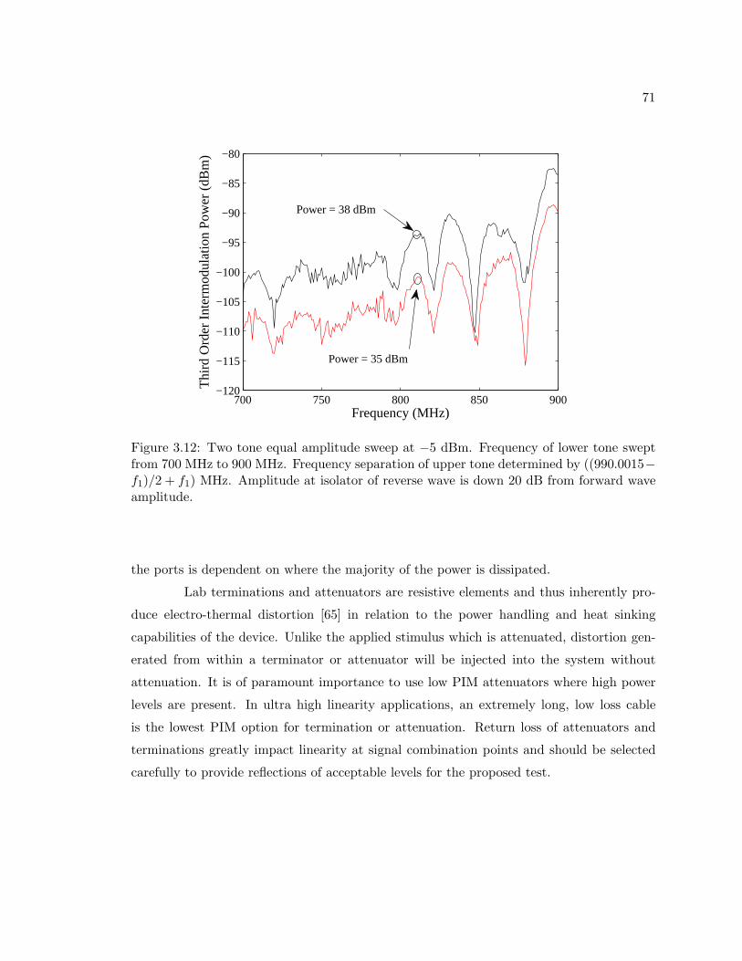
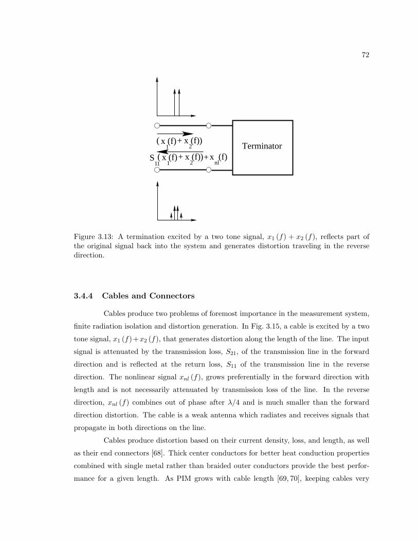
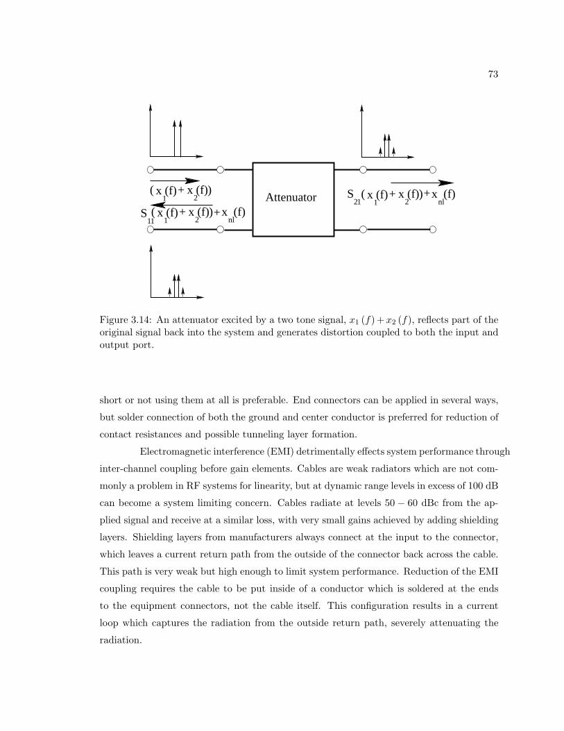
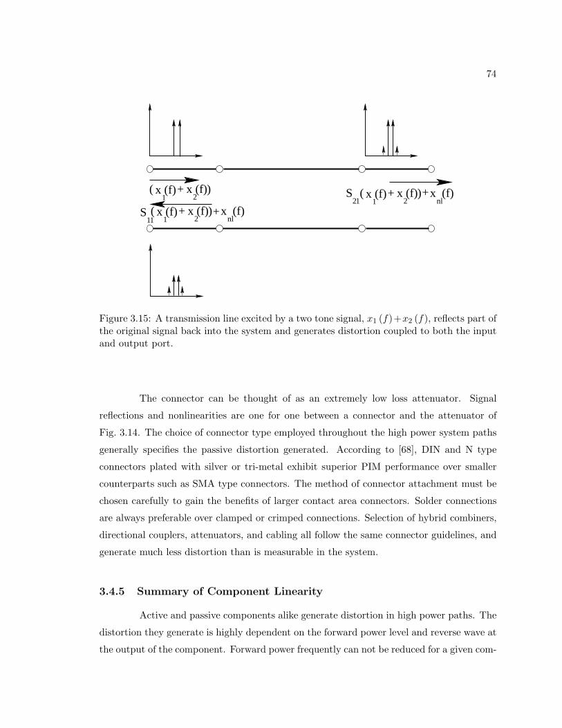
Typical communication links require continually growing power in the transmit
band and sensitivity in the receive band. Interference from spurious signals in the receive
band of a system increases the level of the minimum detectable signal. In narrowband
communications systems, such spurious frequency content manifests itself as nonlinear gen-
eration of additional frequency content related to the input signal. This new frequency
content can be transmitted or coupled to the receive channel, potentially blocking it from
use or substantially reducing the channel signal to interference ratio [1–5].
Increasing coverage areas, bandwidth, and capacity usually leads to a need for
larger link budgets. Such high budget links are normally found in shipboard antennas,
ground stations, antennas for satellite communications, and wireless telecommunication
systems. In these high power systems, signal paths must be kept highly linear. Nonlinear
frequency content arises from the active components in these systems, but in general these
products can be filtered or reduced through feed-forward methods to produce the required
linear signal. Intermodulation distortion generated by passive, linear elements such as
filters, transmission lines, connectors, attenuators, and circulators cannot be removed in
this manner. Distortion of this type is commonly called Passive Intermodulation Distortion
(PIM). Passive distortion is a weakly nonlinear effect, but due to the combination of high
power transmitters and collocated low noise receivers in communications systems, it becomes
the system limiting source of spurious frequency content and thus one of the major factors
limiting the ability to develop highly linear systems.
1.2 Overview
Passive intermodulation distortion is the distortion generated by passive compo-
nents in the system. The processes responsible for PIM generation are weakly nonlinear
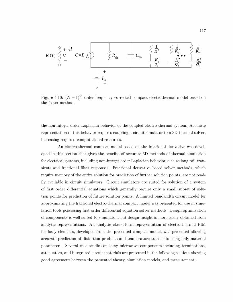
and abundant, with many processes thought to produce similar distortion amplitudes [6,7].
Processes thought to be responsible for PIM generation include contact nonlinearities such
as metal-metal and metal-oxide-metal contacts and material nonlinearities such as ferro-
magnetics, piezoelectrics, ferroelectrics, carbon fibers, kovar, non-linear material conduc-
tivity, and any other material property leading to nonlinear I-V characteristics in the ma-
3
terial [1–3, 5, 8–10]. Attempts have been made to physically explain the sources of PIM,
but due to the sheer number of effects and the similarity of their physical mechanisms cou-
pled with the inherent difficulty in PIM measurement, no definitive PIM mechanism has
emerged.
A base physical mechanism of PIM is examined in this work, electro-thermal con-
ductivity modulation. Electro-thermal conductivity modulation is present in every facet
of passive communications systems. This dissertation aims to explain and derive electro-
thermal distortion across the major design components associated with a communications
system including lumped components, distributed structures, and resonant structures. The
development of a measurement system with unprecedented dynamic range is presented to fa-
cilitate measurement of PIM. The results of this work can be used to design higher linearity
and reduced co-site interference communications systems.
1.2.1 Passive Distortion Modeling
Exact physics or mechanisms of passive distortion are not known conclusively, thus
very few physically-based models are available. Behavioral approaches are frequently used in
lieu of physically-based solutions to model the total observed dynamic of a system [3,11–13].
Behavioral modeling works well for repeatable, time-invariant processes, but PIM distortion
can be dynamic and can vary widely under the same measurement conditions [4,10,13]. This
behavior could be from measurement, as PIM is extremely difficult to measure due to the
weakness of the nonlinearity, or could be a property of the PIM process. Behavioral models
give a general idea of the trends of device performance but are not generally accurate for
high performance design. Physically-based models, if obtainable, allow accurate prediction
of system performance. The foremost objective of this work is the production of physical
models for dominant passive distortion mechanisms.
1.2.2 Passive Intermodulation Measurement
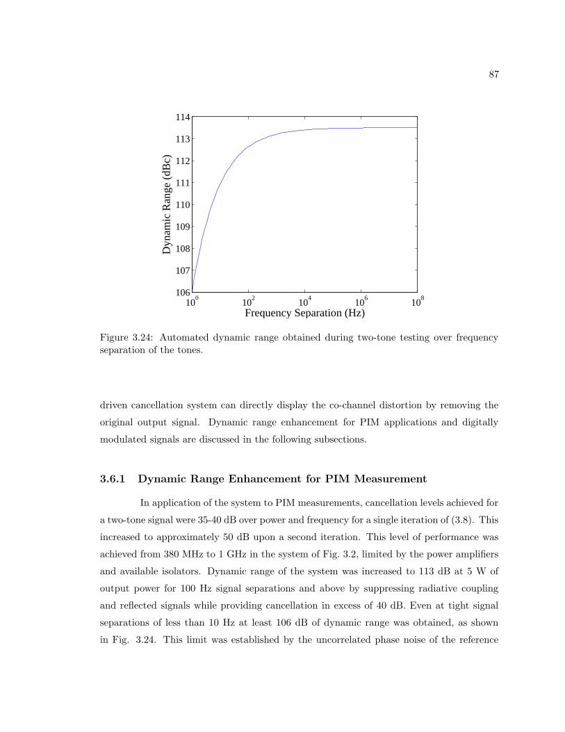
Measurement of PIM requires system spurious free dynamic ranges on the order
of 100 to 160 dBc at high power, depending on the component under test [10, 13]. Most
commercial spectrum analyzers provide only 75 dB of dynamic range even at optimal input
4
conditions. Adding to the difficulty is the requirement that every active and passive com-
ponent in the system produce less distortion than the required dynamic range. Attenuation
could be introduced to reduce or eliminate receiver nonlinearity, but this will both reduce
the magnitude of nonlinearities and increase noise. To reduce both noise and carrier level
simultaneously, filtering or active feed-forward techniques are needed. Filtering is an ex-
tremely effective technique and is used in most PIM measurements to date. Unfortunately,
this method is limited by filter bandwidths and the sharpness of duplexer skirts, and is not
tunable without physically changing filters to cover other frequency bands [14]. Measure-
ments are limited in this method to several megahertz separation, which is not adequate
for measurement of all amplitude modulated signals. PIM is often frequency and ampli-
tude modulation dependent, thus a method allowing accurate PIM measurement regardless
of frequency or signal type is needed. Such a system is developed in this work, employing
feed-forward cancellation in order to provide tunable, bandwidth independent measurement
capabilities for PIM measurement.
1.2.3 Objective: Explain and Model the physical source of PIM
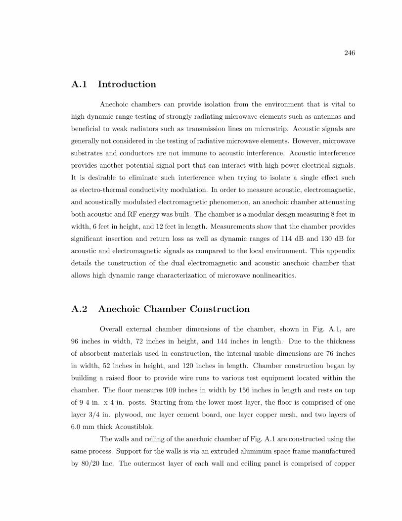
There are four main aspects of this work:
• The analytic derivation of the physics behind electro-thermal distortion in general
lossy microwave components and corresponding simulation models.
• The physical derivation and model development for distributed passive intermodula-
tion including forward and reverse wave growth on a transmission line.
• The determination of PIM mechanisms in antennas and a simulation tool to predict
antenna PIM performance.
• The development of a ultra-high dynamic range, broadband PIM measurement system
based on feed-forward cancellation.
5
1.3 Original Contributions
A number of original research initiatives were undertaken and are described in this
dissertation. The author’s contributions to the field of RF and microwave engineering are
summarized below.
1.3.1 Broadband High Dynamic Range Measurement System
Passive intermodulation distortion is a weakly nonlinear process. It is generated
in the presence of high power signals. These signals will either saturate the receiver used
for measurement or mask the much smaller signals. A system capable of measuring small
signals in the presence of large signals is needed to enable PIM measurement.
A PIM measurement system based on feed-forward cancellation is developed. The
system reduces the linear applied signal and corresponding noise, increasing the relative
magnitude of the distortion products. A formula for automatic cancellation is developed,
resulting in a wideband, high dynamic range system well suited for PIM measurement.
1.3.2 Nonlinear Electro-Thermal Theory
Electro-thermal PIM in microwave systems is a baseline for system performance
as it exists in every conductor. Electro-thermal theory as it applies to distortion at RF
and microwave frequencies is derived from base physics for the first time to the author’s
knowledge for lumped lossy components, distributed structures, and resonant structures.
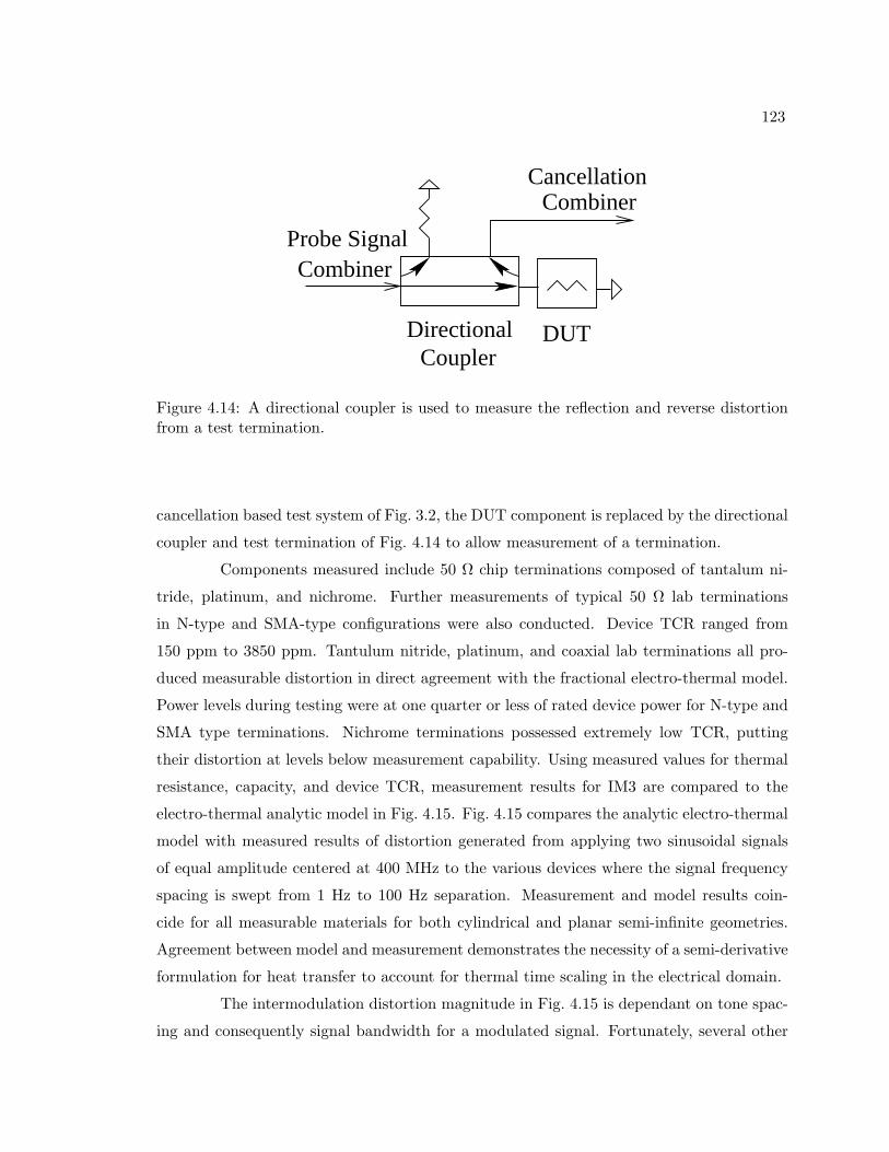
1.3.3 Fractional Electro-Thermal Circuit Model
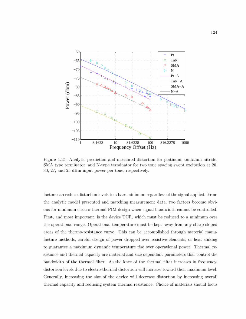
Circuit models for coupled physical phenomena are desirable to minimize simula-
tion time in complex circuits. Often finite difference and element methods are too com-
putationally intensive to allow coupling electrical circuit simulation with other physics in
nonlinear systems.
A highly accurate physically based circuit model was developed based on heat
conduction theory and the fractional derivative. The model allows accurate simulation of
electro-thermal coupling in large scale circuit simulators over all frequency.
6
1.3.4 Foster Expansion Electro-Thermal Circuit Model
Commercial simulators do not possess routines for computation of fractional deriva-
tives. An approximate method is desirable to impart the ability to simulate electro-thermal
processes with a slightly diminished level of accuracy. A circuit model based on a fos-
ter fit of the electro-thermal response is developed to facilitate approximate simulation in
commercial simulators over limited bandwidths.
1.3.5 Distributed PIM Model
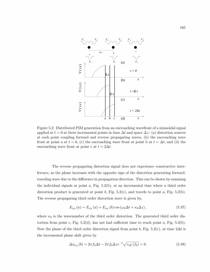
Transmission lines and circuit elements constructed from them generate PIM that
varies with transmission line structure, dimensions, and materials. Rules of thumb exist to
minimize PIM on these structures, but a physically-based theory is needed to accurately
model performance. A physically-derived model is presented for distributed PIM generation.
1.3.6 Resonant PIM Model
Antennas generate PIM that varies with structure, dimensions, and materials used
to construct the device. Little is known of PIM generation mechanisms in antennas. A
base physical mechanism of PIM generation is isolated and a physically-derived model is
presented for resonant PIM generation.
1.3.7 Electromagnetic and Acoustic Anechoic Chamber
An anechoic chamber is designed and constructed to allow measurement of both
electromagnetic and acoustic signals in a shielded environment with reduced reflection. The
chamber allows single and mixed domain measurement.
1.4 Dissertation Outline
Chapter two of this dissertation gives a literature review of PIM processes, PIM re-
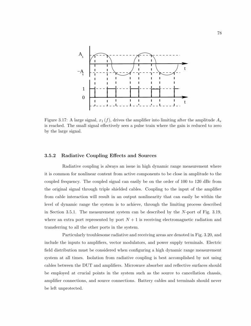
search, distortion analysis, distortion measurement, and mathematical techniques necessary
for PIM modeling.
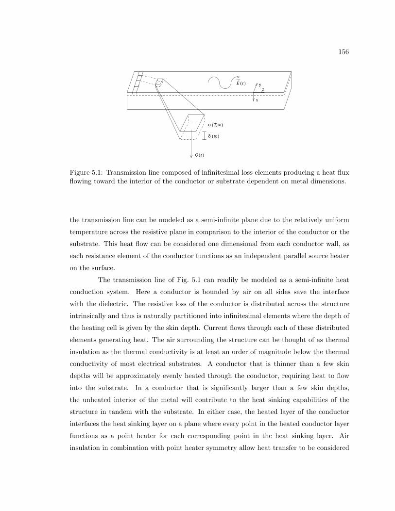
7
Chapter three discusses broadband high dynamic nonlinear measurement. Feed-
forward cancellation theory is presented along side techniques for implementing a linear
feed-forward system. Measurement of nonlinearities require that the components be more
linear than the device under test. Linearity against both forward and reverse waves are
presented for each type of component in the developed measurement system. Reflections,
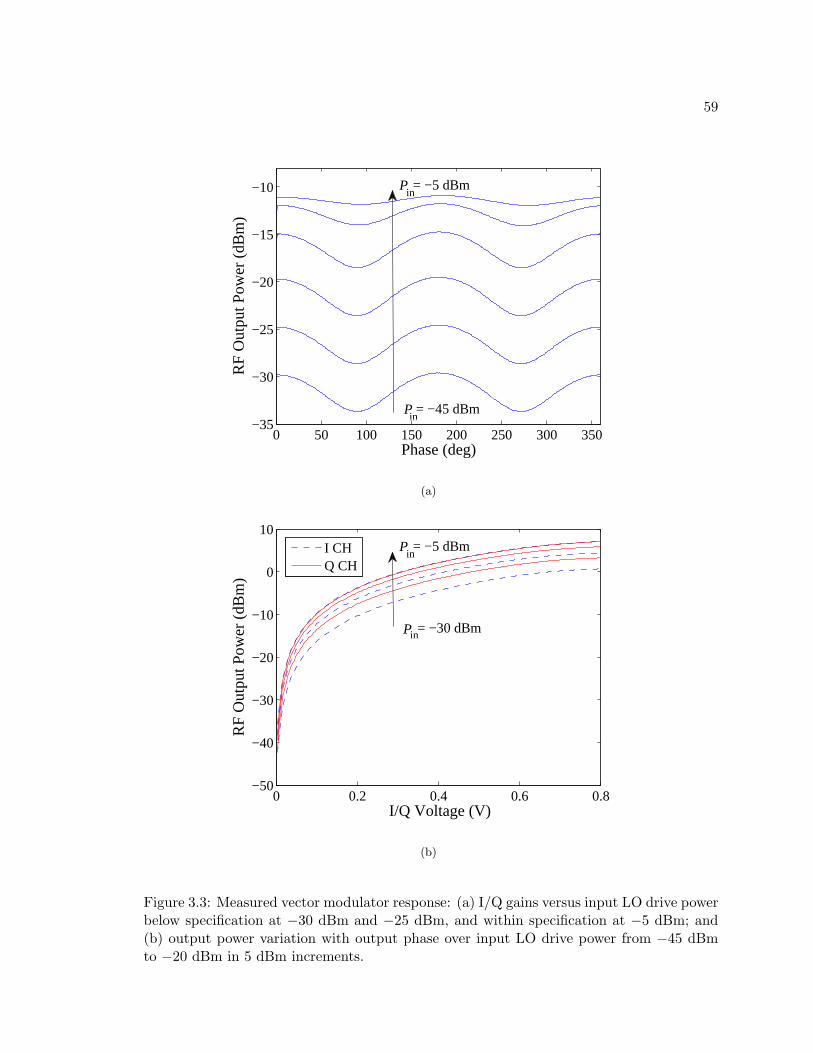
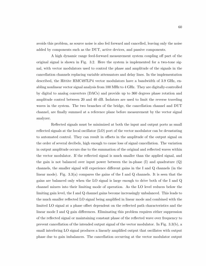
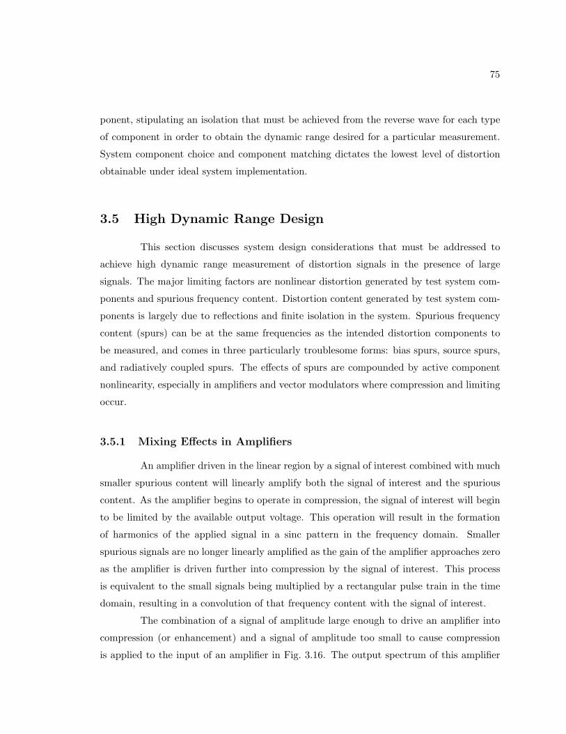
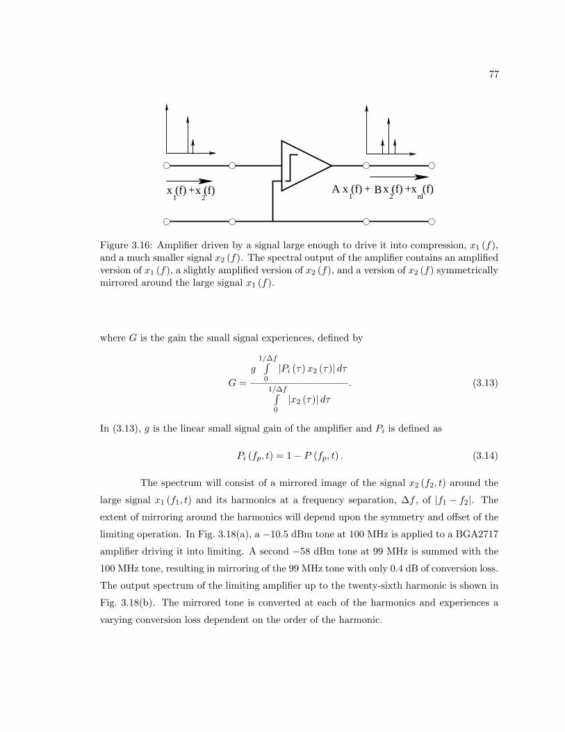
finite isolation, and coupling are discussed in the context of linearity effects on the system.
System performance for two-tone PIM measurement and in-band distortion in wideband
signals is presented.
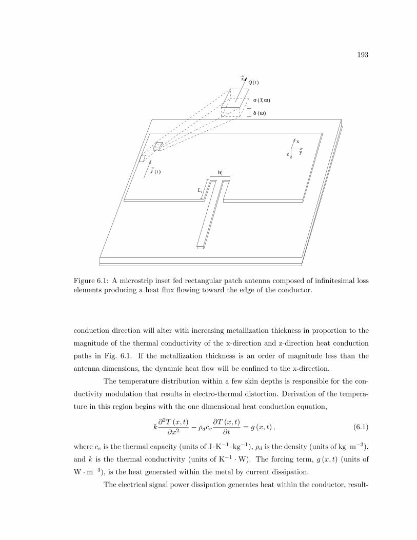
Chapter four delves into the electro-thermal process responsible for PIM in lossy
lumped components. The heat conduction environment for general lumped components and
the corresponding electrical and thermal domain coupling is analyzed resulting in a frac-
tional electro-thermal model which correctly accounts for the long tail transients seen in
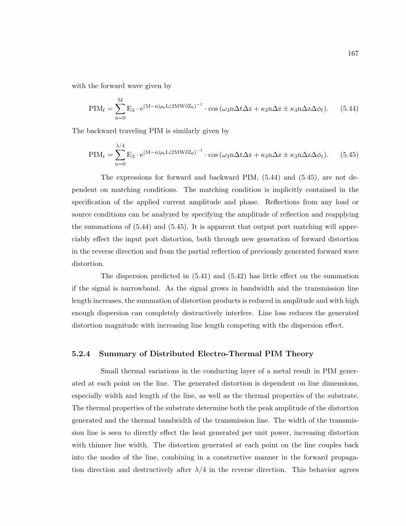
these devices. A circuit model based on the fractional derivative and an approximate model
based on foster expansion is presented. Several cases of interest including microwave termi-
nations, platinum attenuators, and integrated circuit polysilicon electro-thermal distortion
are explored.
Chapter five takes a look at the PIM in a distributed structure such as a trans-
mission line. The PIM is found to be electro-thermal in nature in each infinitesimal lossy
section of the transmission line. The growth and decay of PIM with line length in both
forward and reverse propagation directions is presented. Transmission line samples, silver
on quartz and silver on sapphire, are manufactured isolating the electro-thermal process.
A simulation model for prediction of PIM from material parameters and transmission line
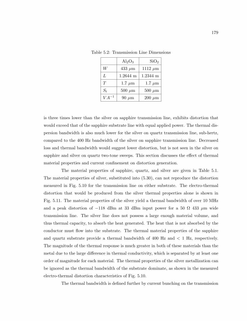
dimensions is presented.
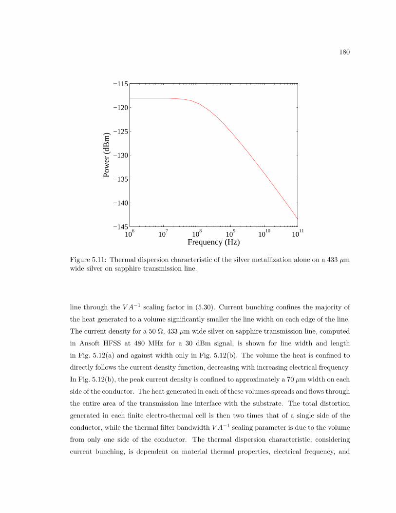
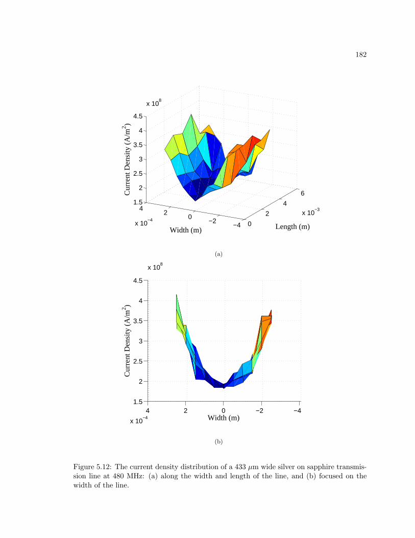
Chapter six explorers PIM production in resonant structures. Antennas are man-
ufactured on both FR4 and sapphire to isolate the distortion, which is shown to be electro-
thermal in nature. A physical model based on current distributions is discussed leading to
a simulation model for prediction of PIM on an antenna.
Chapter seven contains a summary of the work performed and lists the significant
outcomes of this work.
8
1.5 Published Works
1.5.1 Journals
1. J. R. Wilkerson, K. G. Gard, A. G. Schuchinsky, and M. B. Steer, “Theory of Electro-
Thermal Distortion in Lossy Microwave Components,” IEEE Trans. on Microwave Theory
and Techniques, Dec 2008, pp. 2717-2725.
1.5.2 Conferences
1. A. Walker, J. Wilkerson, K. Gard and M. B. Steer, “Modeling and characterization
of the intermodulation response of a remote nonlinear system,” Government Microcircuit
Applications Conf. (GOMACTech), Mar. 2006.
2. J. R. Wilkerson, K. G. Gard and M. B. Steer, “Electro-thermal passive intermodulation
distortion in microwave attenuators,” 36th European Microwave Conference, Sep. 2006, pp.
157-160.
3. K. Gard, J. Wilkerson and M. Steer, “Electro-thermal generation of intermodulation
distortion in film resistors,” Government Microcircuit Applications Conf. (GOMACTech),
March 2007.
4. M. B. Steer, G. Mazzaro, J. R. Wilkerson and K. G. Gard, “Time-frequency effects in
microwave and radio frequency electronics,” Int. Conf. on Signal Processing and Commu-
nication Systems (ICSPCS,2007), Dec. 2007.
5. J. R. Wilkerson, K. G. Gard, and M. B. Steer, “Wideband High Dynamic Range Dis-
tortion Measurement,” IEEE Radio and Wireless Symposium (RWS,2008), Jan. 2008, pp.
415-418.
6. Glenwood Garner III, Jonathan Wilkerson, Michael M. Skeen, Daniel F. Patrick, Ryan
D. Hodges, Ryan D. Schimizzi, Saket R. Vora, Zhiping Feng, Kevin G. Gard, and Michael.
B. Steer, “Acoustic-RF anechoic chamber construction and evaluation,” IEEE Radio and
Wireless Symposium (RWS,2008), Jan. 2008, pp. 331-334.
7. J. Wilkerson, K. Gard, and M. B. Steer, “Broadband high dynamic range inverse standoff
analysis,” Government Microcircuit Applications Conf. (GOMACTech), Mar. 2008.
8. J. Wilkerson , K. Gard, and M. B. Steer, “Distributed Passive Intermodulation Distor-
tion,” Government Microcircuit Applications Conf. (GOMACTech), Mar. 2009.
9
9. J. Wilkerson and M. B. Steer, “Passive Intermodulation Distortion in Antennas,” Gov-
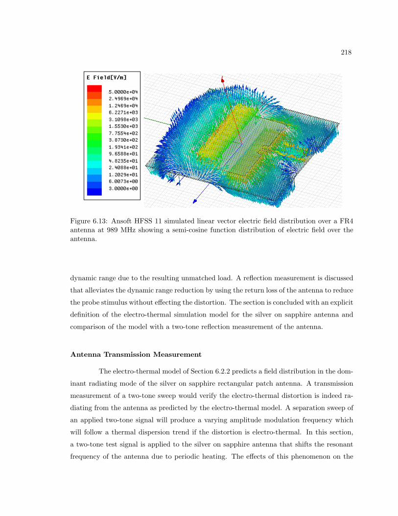
ernment Microcircuit Applications Conf. (GOMACTech), Mar. 2010.
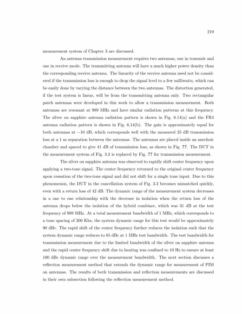
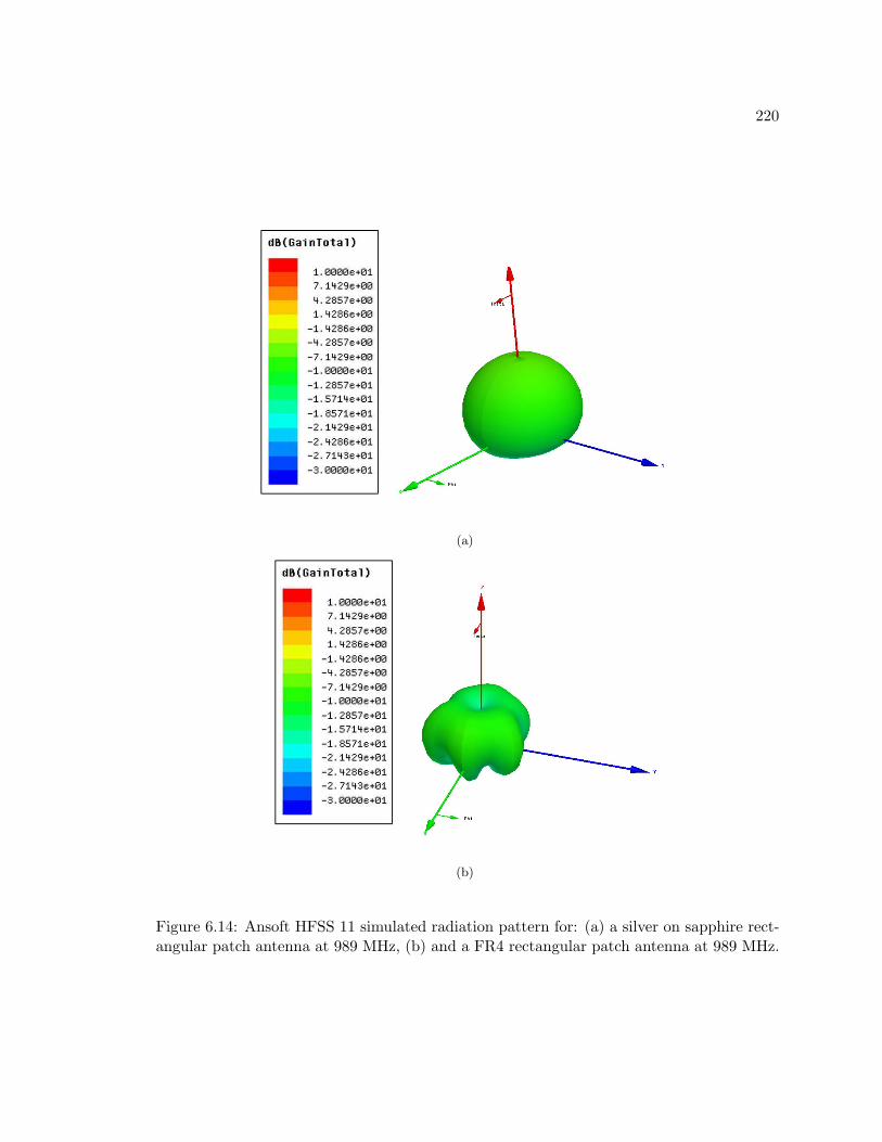
1.6 Unpublished Works
1. J. R. Wilkerson, K. G. Gard, and M. B. Steer, “Automated Broadband High Dy-
namic Range Nonlinear Distortion Measurement System,” submitted to IEEE Trans. on
Microwave Theory and Techniques, Sep 2009.
2. J. R. Wilkerson, P. Lam, K. G. Gard, and M. B. Steer, “Distributed Passive Intermodu-
lation Distortion in Transmission Lines,” submitted to IEEE Trans. on Microwave Theory
and Techniques, Feb. 2010.
3. J. R. Wilkerson, P. Lam, K. G. Gard, and M. B. Steer, “Passive Intermodulation
Distortion in Antennas,” submitted to IEEE Trans. on Microwave Theory and Techniques,
Feb. 2010.
10
2
Review of Nonlinear Analysis and
Measurement Techniques
11
2.1 Introduction
Linear system behavior is strived for but in reality can never be achieved due to
the intrinsic nonlinearity of all systems. The non-ideal behavior of systems results in the
generation of new frequency content. This content is of both harmonic and cross modulation
nature. Harmonic distortion is restricted to all new signals at integer multiples of the input
signal frequency. This type of distortion is usually not problematic as it can be bandpass
filtered from the signal of interest. Unfortunately, cross or intermodulation distortion, is
much more difficult to design out of a system due to the proximity in frequency of many
cross modulation components to the original signal.
Intermodulation distortion occurs when signals with more than one frequency are
input to a system. As implied by the name, each frequency component crosses or mixes
with every other component in the system, even other nonlinear frequency content as pre-
scribed by the nonlinear characteristic of the system. The spectra associated with this
process yields baseband components, as well as the in-band co-channel and adjacent band
frequency components at the fundamental and harmonic responses. While baseband effects
can usually be countered through filtering, in-band components are quite problematic. In-
band co-channel components are at or near the frequency of the fundamental. Components
falling on the fundamental sum with the fundamental as either correlated or uncorrelated
noise, reducing the signal to noise ratio of a channel. In-band adjacent distortion is possibly
the most dangerous of all, as its mixing products can fall within the receive band of either
the generating system or other systems operating in nearby frequency bands. As communi-
cations systems continue to add more capacity, commercial spectrum congestion increases
proliferating mixing products. Generally adjacent distortion is too close to the carriers to
be filtered out, leading to the need for nonlinear system design to eliminate or reduce these
components. Nonlinear modeling breaks distortion processes into that of active devices and
passive devices due to the difference in the relative strength of the the nonlinearities.
Nonlinear system design has conventionally been limited to active devices, which
are known to exhibit strongly nonlinear behavior if operated outside of their linear regime.
Nonlinear responses can be avoided in an active system by operating the circuit under small
signal conditions, or using feedback or more exotic techniques such as pre-distortion to
output a linear response within system requirements. In general active devices are designed
12
to provide a prescribed linearity and are not the limiting factor in system performance.
2.2 Passive Distortion
Passive nonlinearities, contrary to active devices, are weakly nonlinear. Due to
the weakness of the nonlinearity, coupled with modeling difficulty, passive components are
conventionally modeled as linear. This assumption holds until system power levels and dy-
namic range requirements become large, at which point passive nonlinearities can become
the ultimate system limit. Unfortunately passive processes are difficult to measure due to
the massive dynamic range needed to measure the effects [13]. Unlike active distortion,
where the device physics leading to distortion are well modeled, passive devices have many
potential mechanisms that can result in distortion. Most of these processes can happen in
the same physical situation, causing great difficulty in confirmation of the theory associated
with passive processes [1–8, 15]. Enabling systems to be designed for low or no passive
intermodulation distortion (PIM) requires definitive knowledge of the dominant processes
responsible for PIM. Arriving at any conclusion about the nature of PIM requires a broad
knowledge all the possible contributors, which include many different subsets of physics.
A review of the prominent factors potentially affecting passive components is given, differ-
entiating between contact and material based nonlinearity and the corresponding possible
nonlinear processes underlying each.
2.2.1 Metal-Insulator-Metal and Metal-Metal Contact Nonlinearities
At any contact between components, there exists the potential for distortion gener-
ation through a variety of mechanisms. These mechanisms spring from two general physical
situations, the metal-insulator-metal contact (MIM) and the metal-metal (MM) contact.
Thin insulating layers, either oxides or sulphides, are natural to all metals save gold result-
ing in the initial formation of MIM structures at low pressure [11]. As the surfaces are more
intimately contacted, the insulator can be penetrated leaving a metal to metal connection.
The two types of contact can occur in many different manners and concurrently, dependent
upon both the surface topography and the pressure of the contact [10–12,16].
Nominally, the contact area of two conductors in a connector or waveguide would
13
just be the size of the conductor pin or the surface area of the waveguide. Unfortunately,
the nature of such contacts are not as simple as would be preferred, as no material can
be completely smooth. Material surfaces do not enjoy the bond stability of the material
interior [17]. Minimization of the free energy associated with dangling bonds at the material
surface leads to a different lattice structure near the surface, which often grows in islands
due to lattice imperfections. These islands grow at various rates and to various heights,
producing extremely irregular contact areas. Contacting two surfaces of this nature is
closer to contacting many needles of various lengths than a flat surface [11,16]. It becomes
apparent that surface topography limits the actual contact area to a tiny percentage of
the macroscopic contact area. Decreasing loss and increasing reliability would require the
most contact area possible, which can be accomplished to some degree through increasing
connection pressure [11].
The variation of connection pressure will cause the surface properties to change
over three domains of mechanical deformation, elastic, elasto-plastic, and plastic. In the
elastic regime, the pressure is low enough that the surfaces recover their original shape
when taken apart. This region could be thought of as a slight bending of the needles,
where further contact becomes possible to the angling of the needles. The plastic regime
of deformation is the other extreme, forever altering the surface properties of the contact.
This region will provide the most contact area possible and can rupture the insulator layer,
resulting in a much higher percentage of metal-metal contacts. The elasto-plastic region is
a partial permanent deformation of the surface, which could be thought of as a permanent
bending or breakage of longer needles while shorter needles are not permanently affected.
Each of the physical structures, MIM and MM contacts, have several of their
own, distinct nonlinear mechanisms. Metal-insulator-metal structures are most susceptible
to tunneling and thermionic emission. Metal to metal structures can create diode like
junctions due to differences in metal work functions as well as nonlinear contact resistances
due to thermal processes including thermal expansion of the material and thermal resistance
variation.
14
Tunneling
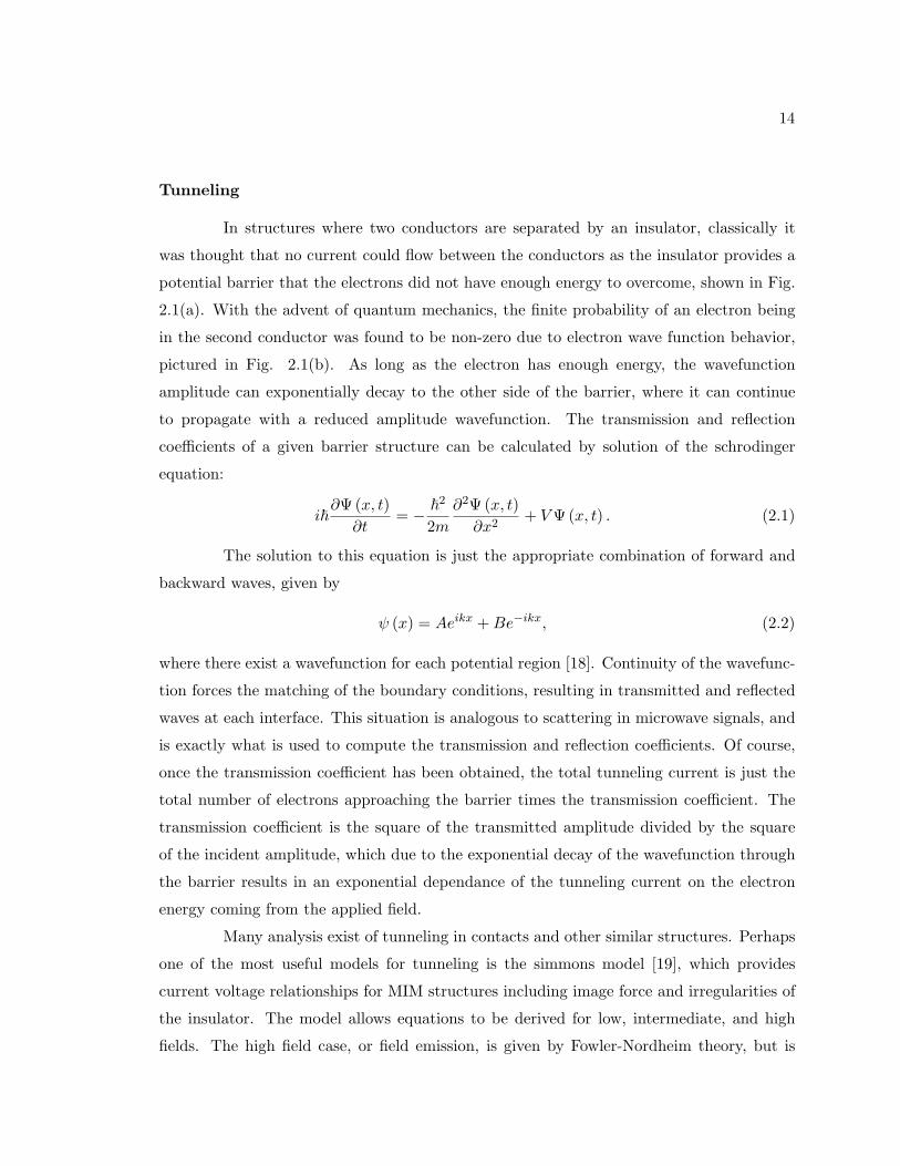
In structures where two conductors are separated by an insulator, classically it
was thought that no current could flow between the conductors as the insulator provides a
potential barrier that the electrons did not have enough energy to overcome, shown in Fig.
2.1(a). With the advent of quantum mechanics, the finite probability of an electron being
in the second conductor was found to be non-zero due to electron wave function behavior,
pictured in Fig. 2.1(b). As long as the electron has enough energy, the wavefunction
amplitude can exponentially decay to the other side of the barrier, where it can continue
to propagate with a reduced amplitude wavefunction. The transmission and reflection
coefficients of a given barrier structure can be calculated by solution of the schrodinger
equation:
i~∂Ψ(x, t)
∂t= − ~
2
2m
∂2Ψ(x, t)∂x2
+ V Ψ(x, t) . (2.1)
The solution to this equation is just the appropriate combination of forward and
backward waves, given by
ψ (x) = Aeikx + Be−ikx, (2.2)
where there exist a wavefunction for each potential region [18]. Continuity of the wavefunc-
tion forces the matching of the boundary conditions, resulting in transmitted and reflected
waves at each interface. This situation is analogous to scattering in microwave signals, and
is exactly what is used to compute the transmission and reflection coefficients. Of course,
once the transmission coefficient has been obtained, the total tunneling current is just the
total number of electrons approaching the barrier times the transmission coefficient. The
transmission coefficient is the square of the transmitted amplitude divided by the square
of the incident amplitude, which due to the exponential decay of the wavefunction through
the barrier results in an exponential dependance of the tunneling current on the electron
energy coming from the applied field.
Many analysis exist of tunneling in contacts and other similar structures. Perhaps
one of the most useful models for tunneling is the simmons model [19], which provides
current voltage relationships for MIM structures including image force and irregularities of
the insulator. The model allows equations to be derived for low, intermediate, and high
fields. The high field case, or field emission, is given by Fowler-Nordheim theory, but is
15
Metal 2
F1 EF2
VB
Metal 1
Barrier
E
(a)
BarrierF1
EF2
VB
IΨTΨ
Metal 1
Metal 2
VI
E
(b)
Figure 2.1: A metal-oxide-metal barrier under: (a) no applied potential where no tunnelingoccurs, (b) and an applied potential allowing an electron with sufficient energy to tunnel tothe metal on the lower energy side of the barrier.
16
generally not applicable in practical applications. The Simmons’ model is sufficient for low
fields and medium fields, which is our area of interest. The Simmons’ model under medium
field for a generalized barrier provides the tunneling current, given by [19]
J =[6.2× 10¹⁰/ (β∆s)2
]
ϕ exp
(−1.025β∆sϕ−.5)− (ϕ + V ) exp
[−1.025β∆s (ϕ + V ).5
],
(2.3)
where ϕ is the mean barrier height, V is the applied voltage, ∆s is the barrier thickness at
the fermi level, and β is a correction factor that is approximately valued unity.
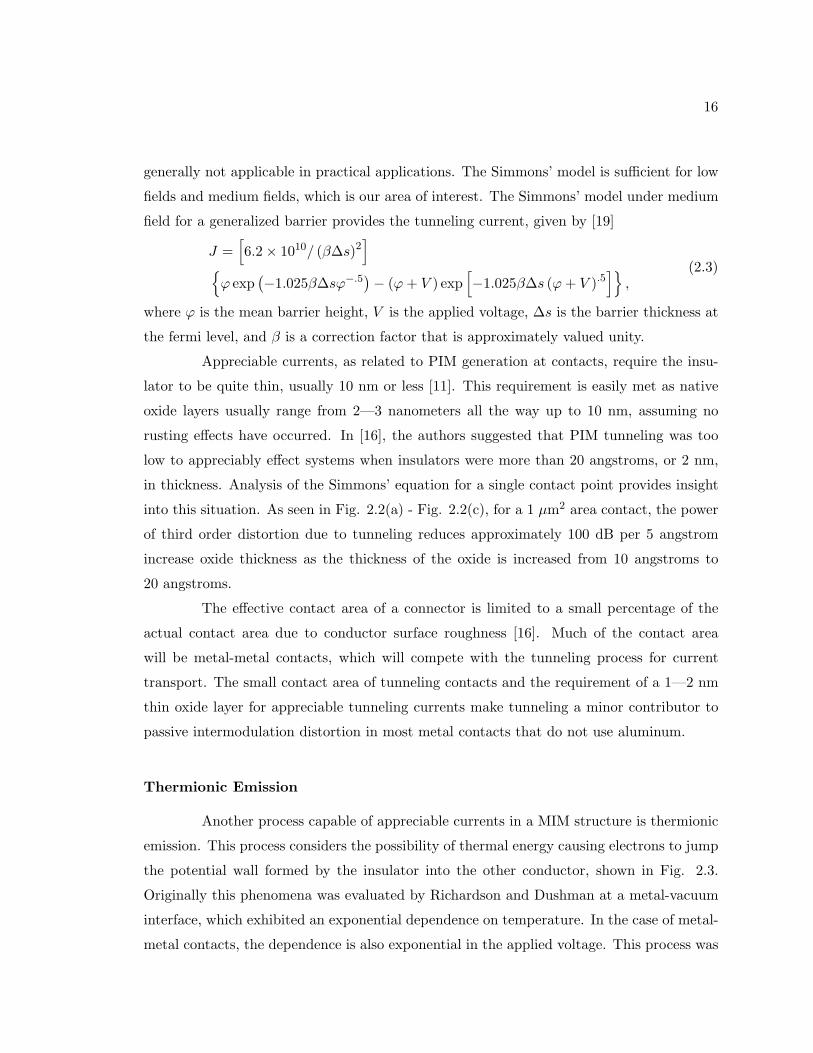
Appreciable currents, as related to PIM generation at contacts, require the insu-
lator to be quite thin, usually 10 nm or less [11]. This requirement is easily met as native
oxide layers usually range from 2—3 nanometers all the way up to 10 nm, assuming no
rusting effects have occurred. In [16], the authors suggested that PIM tunneling was too
low to appreciably effect systems when insulators were more than 20 angstroms, or 2 nm,
in thickness. Analysis of the Simmons’ equation for a single contact point provides insight
into this situation. As seen in Fig. 2.2(a) - Fig. 2.2(c), for a 1 µm2 area contact, the power
of third order distortion due to tunneling reduces approximately 100 dB per 5 angstrom
increase oxide thickness as the thickness of the oxide is increased from 10 angstroms to
20 angstroms.
The effective contact area of a connector is limited to a small percentage of the
actual contact area due to conductor surface roughness [16]. Much of the contact area
will be metal-metal contacts, which will compete with the tunneling process for current
transport. The small contact area of tunneling contacts and the requirement of a 1—2 nm
thin oxide layer for appreciable tunneling currents make tunneling a minor contributor to
passive intermodulation distortion in most metal contacts that do not use aluminum.
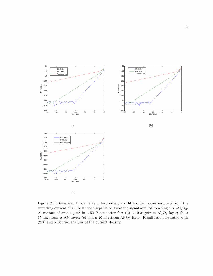
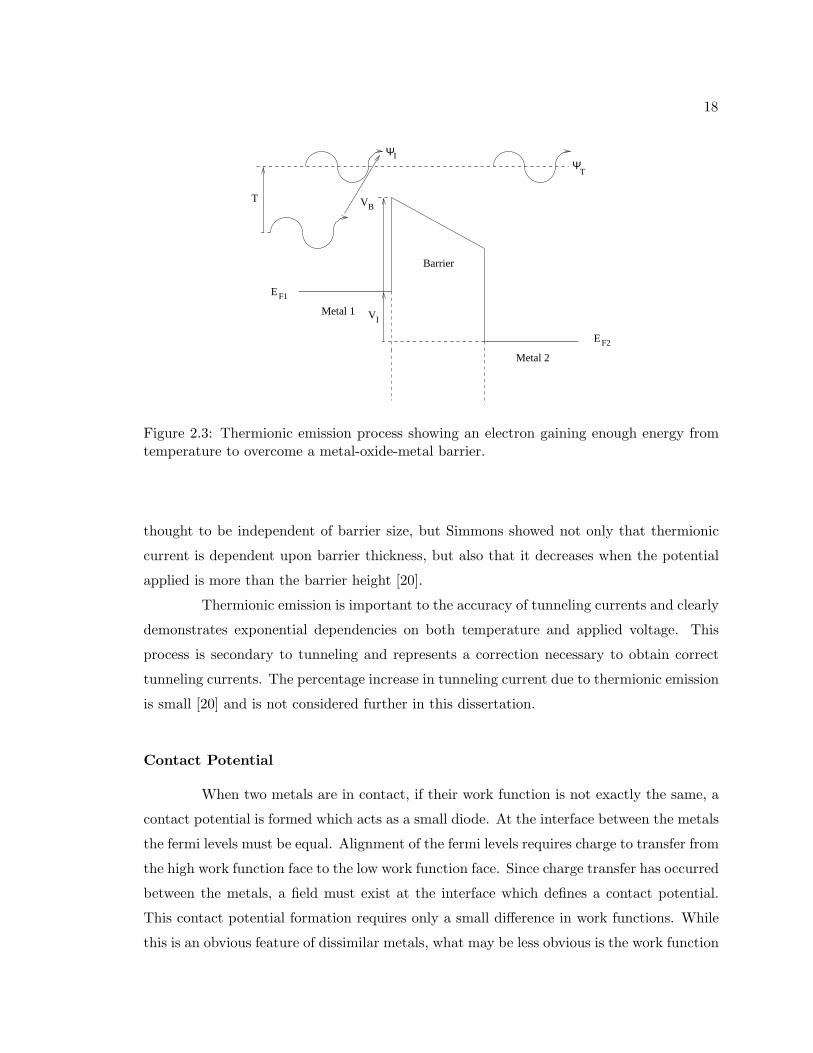
Thermionic Emission
Another process capable of appreciable currents in a MIM structure is thermionic
emission. This process considers the possibility of thermal energy causing electrons to jump
the potential wall formed by the insulator into the other conductor, shown in Fig. 2.3.
Originally this phenomena was evaluated by Richardson and Dushman at a metal-vacuum
interface, which exhibited an exponential dependence on temperature. In the case of metal-
metal contacts, the dependence is also exponential in the applied voltage. This process was
17
−100 −80 −60 −40 −20 0 20−400
−350
−300
−250
−200
−150
−100
−50
0
50
Pou
t (dB
m)
Pin (dBm)
5th Order3rd OrderFundamental
(a)
−100 −80 −60 −40 −20 0 20−500
−450
−400
−350
−300
−250
−200
−150
−100
−50
Pin (dBm)
Pou
t (dB
m)
5th Order3rd OrderFundamental
(b)
−100 −80 −60 −40 −20 0 20−600
−550
−500
−450
−400
−350
−300
−250
−200
−150
−100
Pin (dBm)
Pou
t (dB
m)
5th Order3rd OrderFundamental
(c)
Figure 2.2: Simulated fundamental, third order, and fifth order power resulting from thetunneling current of a 1 MHz tone separation two-tone signal applied to a single Al-Al2O3-Al contact of area 1 µm2 in a 50 Ω connector for: (a) a 10 angstrom Al2O3 layer; (b) a15 angstrom Al2O3 layer; (c) and a 20 angstrom Al2O3 layer. Results are calculated with(2.3) and a Fourier analysis of the current density.
18
I
F1
EF2
VB
ΨT
Metal 1
Metal 2
Barrier
VI
T
Ψ
E
Figure 2.3: Thermionic emission process showing an electron gaining enough energy fromtemperature to overcome a metal-oxide-metal barrier.
thought to be independent of barrier size, but Simmons showed not only that thermionic
current is dependent upon barrier thickness, but also that it decreases when the potential
applied is more than the barrier height [20].
Thermionic emission is important to the accuracy of tunneling currents and clearly
demonstrates exponential dependencies on both temperature and applied voltage. This
process is secondary to tunneling and represents a correction necessary to obtain correct
tunneling currents. The percentage increase in tunneling current due to thermionic emission
is small [20] and is not considered further in this dissertation.
Contact Potential
When two metals are in contact, if their work function is not exactly the same, a
contact potential is formed which acts as a small diode. At the interface between the metals
the fermi levels must be equal. Alignment of the fermi levels requires charge to transfer from
the high work function face to the low work function face. Since charge transfer has occurred
between the metals, a field must exist at the interface which defines a contact potential.
This contact potential formation requires only a small difference in work functions. While
this is an obvious feature of dissimilar metals, what may be less obvious is the work function
19
AirAir Air
Metal
Metal
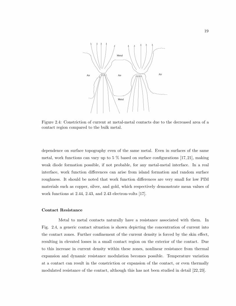
Figure 2.4: Constriction of current at metal-metal contacts due to the decreased area of acontact region compared to the bulk metal.
dependence on surface topography even of the same metal. Even in surfaces of the same
metal, work functions can vary up to 5 % based on surface configurations [17, 21], making
weak diode formation possible, if not probable, for any metal-metal interface. In a real
interface, work function differences can arise from island formation and random surface
roughness. It should be noted that work function differences are very small for low PIM
materials such as copper, silver, and gold, which respectively demonstrate mean values of
work functions at 2.44, 2.43, and 2.43 electron-volts [17].
Contact Resistance
Metal to metal contacts naturally have a resistance associated with them. In
Fig. 2.4, a generic contact situation is shown depicting the concentration of current into
the contact zones. Further confinement of the current density is forced by the skin effect,
resulting in elevated losses in a small contact region on the exterior of the contact. Due
to this increase in current density within these zones, nonlinear resistance from thermal
expansion and dynamic resistance modulation becomes possible. Temperature variation
at a contact can result in the constriction or expansion of the contact, or even thermally
modulated resistance of the contact, although this has not been studied in detail [22, 23].
20
2.2.2 Ferromagnetic Material Nonlinearity
Ferromagnetic materials such as iron, steel, cobalt, and nickel are often used for
mechanical structures supporting antennas and construction or plating of connectors and
cables as well as in the production of transformers and circulators. The metals are known
to produce much higher levels of distortion than structures composed of diamagnetic metals
[24–27] such as copper, silver, and gold. The basis for the nonlinear nature of these materials
lies in the magnetic field dependance of their permeability. A brief review of magnetization
is necessary in order to explain the nonlinear behavior of ferromagnetic metals.
The origin of magnetic moments arises on an atomic level from both the spin
and orbit of an electron. An atom’s total magnetic moment is the summation of electron
spin-spin, spin-orbit, and orbit-orbit interactions. Since total spin must be maximized in
order for magnetization to occur, it is only witnessed in materials with incomplete electron
shells, which is strongest when near half full. A further restriction of ferromagnetism is
the necessity for the atomic structure to allow the magnetic dipole moments to align in
parallel. Of course the energy from this process, coulomb repulsion, must be minimized
along with all addition magnetic energies in the material, which include magnetostatic,
magnetorestrictive, and magnetocrystalline energies [21,28].
Magnetorestrictive energy is the external magnetic field generated around the ma-
terial. Since this field can and will perform work, it must be minimized. If all magnetic
dipole moments in the material align in a single direction, the largest possible external field
would be generated while at the same time minimizing coulomb repulsion. This statement
suggest minimization of the potential can be accomplished by increasing the number of
magnetic domains in such an order and directionality as to limit the external field. Magne-
torestrictive energy also prefers smaller domains in order to minimize the elastic strain in-
duced on the lattice. Counterbalancing these requirements is the magnetocrystalline energy,
which desires large domains in order to minimize the total number of domain walls. Domain
wall minimization arises from the crystal property of unequal magnetization impedance in
various crystallographic directions. As the domain magnetic alignment will be in a low
impedance direction, the domain walls must necessarily be in high impedance directions,
increasing system energy. The balancing of these energies leads to a structure with many
domains oriented with 90 or 180 degree walls with respect to each other [21,28].
21
B
cH−
B
B−
− s
r
Hc
rB
Bs
H
Figure 2.5: Magnetic hysteresis loop defined by saturation magnetization, Bs, remnantmagnetization, Br, and the coercive magnetic field, Hc.
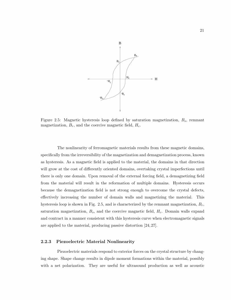
The nonlinearity of ferromagnetic materials results from these magnetic domains,
specifically from the irreversibility of the magnetization and demagnetization process, known
as hysteresis. As a magnetic field is applied to the material, the domains in that direction
will grow at the cost of differently oriented domains, overtaking crystal imperfections until
there is only one domain. Upon removal of the external forcing field, a demagnetizing field
from the material will result in the reformation of multiple domains. Hysteresis occurs
because the demagnetization field is not strong enough to overcome the crystal defects,
effectively increasing the number of domain walls and magnetizing the material. This
hysteresis loop is shown in Fig. 2.5, and is characterized by the remnant magnetization, Br,
saturation magnetization, Bs, and the coercive magnetic field, Hc. Domain walls expand
and contract in a manner consistent with this hysteresis curve when electromagnetic signals
are applied to the material, producing passive distortion [24,27].
2.2.3 Piezoelectric Material Nonlinearity
Piezoelectric materials respond to exterior forces on the crystal structure by chang-
ing shape. Shape change results in dipole moment formations within the material, possibly
with a net polarization. They are useful for ultrasound production as well as acoustic
22
mode SAW and BAW filters. Ferroelectric materials are a special subset of piezoelectric
materials, and are of great interest as they allow for tunable capacitors, which can provide
dynamic matching networks. Ferroelectric materials are also increasingly being integrated
as filler materials in circuit board manufacture. Unlike standard dielectrics that do not keep
a residual polarization, ferroelectric materials exhibit polarization memory with reversible
polarity. Much like ferromagnetic devices, the electric field dependance on the polarization
vector leads to nonlinear behavior in these devices [29,30].
In a piezoelectric material, each unit cell of the material is non-centrosymmetic.
If the unit cell had a structure that possessed a center of symmetry, any dipole moment
generated by one cell would cancel the corresponding cell by symmetry. The center atom
of the unit cell of this material must thus be able to occupy a non-equilibrium position
due to local dipole moments throughout the material. This dipole moment can either be
spontaneous, as in the case of ferroelectric materials where a net polarization accumulates,
or can occur from stress in non-spontaneous polarization, as occurs in quartz [29].
Much like the case of ferromagnetic materials, ferroelectric nonlinearity is based
on domain growth and reversal. In this case stray electric field energy, instead of magnetic
field, must be minimized. The material, before field application, will have domains that
are aligned such that dipole moments of individual domains meet at 90 and 180 degree
angles in a manner that minimizes all excess field energy outside the material. When a
field is applied to one of these directions, the direction of parallel alignment with the field
is reduced in energy while all other components are increased in energy. Minimization
of internal energy will cause the parallel domains to grow, overtaking other domains and
crystal defects, eventually resulting in only domains directed with the field. When the
field is released, the material will once again seek to minimize the energy by forming new
domains aligned in other directions. Since the material cannot return to a neutral position
in the cells, a net polarization will remain which is irreversible, although application of a
reverse field can change the polarity of the polarization [29–32]. This process results in a
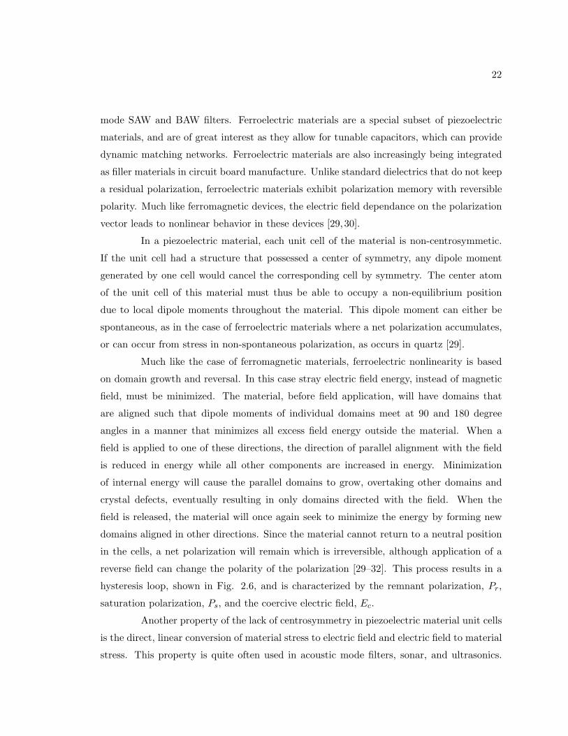
hysteresis loop, shown in Fig. 2.6, and is characterized by the remnant polarization, Pr,
saturation polarization, Ps, and the coercive electric field, Ec.
Another property of the lack of centrosymmetry in piezoelectric material unit cells
is the direct, linear conversion of material stress to electric field and electric field to material
stress. This property is quite often used in acoustic mode filters, sonar, and ultrasonics.
23
Ec−
s
r
Ec
r
s
E
P
−
P−P
P
P
Figure 2.6: Polarization hysteresis loop defined by saturation polarization, Ps, remnantpolarization, Pr, and the coercive electric field, Ec.
This property is often overlooked, but still important to passive distortion as it provides a
direction mechanism for acoustic and mechanical distortion to couple into electrical systems,
with only some applied stress on the material present. Since coming into contact with any
other material provides stress, any material, even electrically neutral materials, that can
exhibit non-spontaneous dipole moments under stress can be potential medium for vibra-
tional and acoustic coupling. This dependence can result in either modulation of electrical
signals, or the more troubling possibility of the introduction of acoustic nonlinearities.
2.2.4 Acoustic Nonlinearities
Acoustics are increasingly integrated with electrical systems through piezoelectrics
as transducers, filters, and even memory components. These systems, while valuable, also
present new challenges in nonlinear system design. Nonlinearities and spurious signals
from acoustic systems are often converted with high efficiencies into the electrical domain,
demanding their analysis as distortion generators. Acoustic nonlinear processes due to
inelasticity is briefly reviewed here.
Inelasticity is a natural consequence of the energy of gases, liquids, and solids.
Due to interatomic forces, as atoms or molecules are moved closer and closer together, the
24
repelling force between them increases exponentially [17, 21]. The forces required to reach
this level of repulsion are usually quite high, leading to the linearization that is elastic
behavior under the condition the system is operated at a small power level. Elasticity
predicts a linear relation between the applied force and the resultant motion. When the
system operates outside of this small force requirement, motion becomes a nonlinear function
of the applied force, resulting in generation of harmonic and intermodulation distortion.
These effects are inherent in the atomic structure of materials, but barring a unique
coupling as in piezoelectrics, is quite small. Inelastic effects are amplified, as compared to
the perfect lattice or volume, through defects in materials such as grain boundaries, cracks,
contacting surfaces, and bonded surfaces. The nonlinearity in these cases arises from the
inelasticity of a surface or coupled elasticities that differ [33–37].
2.2.5 Electrical Conductivity Nonlinearity
Electrical conductivity has long been known to have a dependence on the tem-
perature of the metal. Every metal has a finite conductivity due to electron interactions
with lattice imperfections, dopants, the lattice itself, and other electrons. Temperature
affects the situation by increasing the kinetic energy of each component. For each of the
lattice sites this translates to an increase of the amplitude of random thermal variation.
The cross section of scattering interference conduction electrons feel is dependent on this
random thermal variation, resulting in a thermal dependence of the electrical conductivity.
Most metals exhibit this phenomena as an increase in resistance with increasing tempera-
ture, usually linearly, except for a few metals and alloys such as Nichrome which exhibit
nonlinear dependencies on temperature [38]. Semiconductors also exhibit similar depen-
dencies on temperature, but instead of an increase in resistivity a decrease in resistivity
occurs. In semiconductors the increase in conductivity occurs from the thermal excitation
of electrons to the conduction band, offsetting the increase in the scattering cross section.
Active nonlinearities in semiconductors are more strongly nonlinear than thermal processes,
thus thermal nonlinearities in metals will receive the most consideration.
The transfer of electrical energy through a metal will always result in some energy
loss due to the finite conductivity of the metal. This energy is transferred through scattering
to the lattice, which then transfers the energy as phonons through the lattice until it can
25
be expelled as heat out of the material. This process is simply represented by the thermo-
resistance effect [39]:
ρe(T ) = ρe0(1 + αT + βT 2 + ...). (2.4)
Here ρe0 is the static resistivity constant and α and β are constants representing the temper-
ature coefficients of resistance (TCR). The heating through the material is only dependent
on the resistivity and current density through that resistivity in the relationship
Q = J2ρe, (2.5)
where J is the current density vector.
While there is no dispute that this process is nonlinear, thermal processes are
quite slow, especially compared to any signal above a few kilohertz. This fact has steered
most research away from this phenomena, as it suggested that thermal processes could
only have average effects on any appreciably high frequency signal. The exception to this
train of thought concerning passive intermodulation distortion was suggested by Wilcox
and Molmud [23]. They ignored the slow nature of thermal signals and assumed they would
follow the applied microwave signals instantaneously due to the confinement of heat to the
conducting layer of the metallization. No basis was offered for this assumption. The result
of their study was the prediction in coax cable of intermodulation distortion on the order of
−150 to −140 dBm with a two-tone input of 45 dBm per tone, approximately 185 dBc below
the carrier. Such low levels of distortion would suggest other processes to be dominant,
but further analysis of current confinement and surface roughness suggests substantially
higher distortion. As material nonlinearities represent the ultimate performance a system
can obtain, further research of such nonlinearities is warranted. While ferromagnetic and
ferroelectric sources can be eliminated by material choice, electro-thermal nonlinearity can
never be eliminated. Assuming proper design and connection of components, thermal based
distortion is the limiting factor in any component.
2.3 Distortion Analysis Methods
One of the primary problems associated with passive intermodulation distortion
is the lack of accurate models of passive distortion phenomena. Measurement is virtually
26
impossible to match exactly with theory as distortion can invariably be attributed to many
different sources. In general, modeling of PIM processes is either based upon the deriva-
tion of the constitutive equations and their subsequent nonlinear expansion, or the use of a
general nonlinear element fit to measurement to represent all possible processes in a given
situation. Expansion in either case is usually accomplished through a series expansion of
the nonlinear equation, unless analytic solution of the nonlinear equation set is possible.
Expansion of constitutive equations is done either through a power series or volterra series
method, while a general nonlinear element implies a behavioral model, which is a measure-
ment based fit of the nonlinear behavior of the element.
2.3.1 Power Series
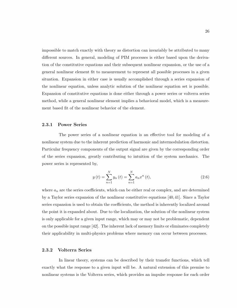
The power series of a nonlinear equation is an effective tool for modeling of a
nonlinear system due to the inherent prediction of harmonic and intermodulation distortion.
Particular frequency components of the output signal are given by the corresponding order
of the series expansion, greatly contributing to intuition of the system mechanics. The
power series is represented by,
y (t) =N∑
n=1
yn (t) =N∑
n=1
anxn (t), (2.6)
where an are the series coefficients, which can be either real or complex, and are determined
by a Taylor series expansion of the nonlinear constitutive equations [40,41]. Since a Taylor
series expansion is used to obtain the coefficients, the method is inherently localized around
the point it is expanded about. Due to the localization, the solution of the nonlinear system
is only applicable for a given input range, which may or may not be problematic, dependent
on the possible input range [42]. The inherent lack of memory limits or eliminates completely
their applicability in multi-physics problems where memory can occur between processes.
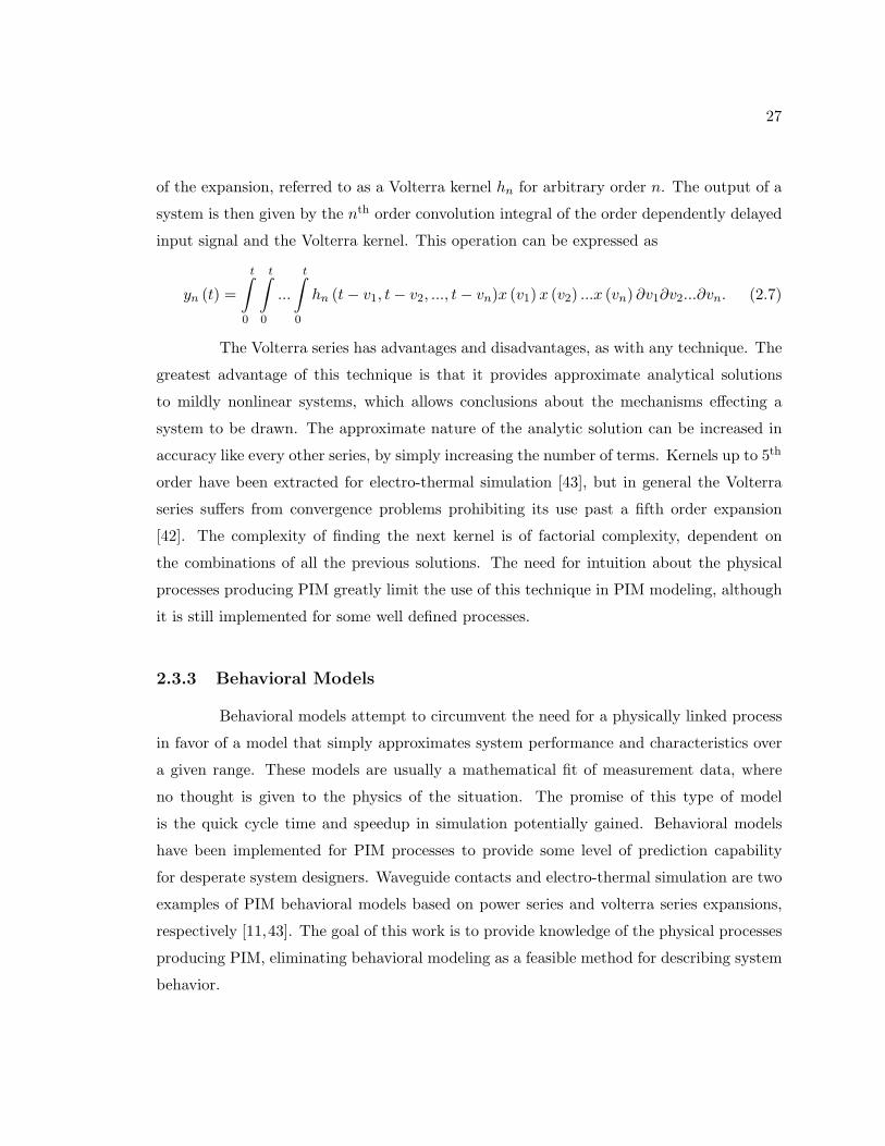
2.3.2 Volterra Series
In linear theory, systems can be described by their transfer functions, which tell
exactly what the response to a given input will be. A natural extension of this premise to
nonlinear systems is the Volterra series, which provides an impulse response for each order
27
of the expansion, referred to as a Volterra kernel hn for arbitrary order n. The output of a
system is then given by the nth order convolution integral of the order dependently delayed
input signal and the Volterra kernel. This operation can be expressed as
The Volterra series has advantages and disadvantages, as with any technique. The
greatest advantage of this technique is that it provides approximate analytical solutions
to mildly nonlinear systems, which allows conclusions about the mechanisms effecting a
system to be drawn. The approximate nature of the analytic solution can be increased in
accuracy like every other series, by simply increasing the number of terms. Kernels up to 5th
order have been extracted for electro-thermal simulation [43], but in general the Volterra
series suffers from convergence problems prohibiting its use past a fifth order expansion
[42]. The complexity of finding the next kernel is of factorial complexity, dependent on
the combinations of all the previous solutions. The need for intuition about the physical
processes producing PIM greatly limit the use of this technique in PIM modeling, although
it is still implemented for some well defined processes.
2.3.3 Behavioral Models
Behavioral models attempt to circumvent the need for a physically linked process
in favor of a model that simply approximates system performance and characteristics over
a given range. These models are usually a mathematical fit of measurement data, where
no thought is given to the physics of the situation. The promise of this type of model
is the quick cycle time and speedup in simulation potentially gained. Behavioral models
have been implemented for PIM processes to provide some level of prediction capability
for desperate system designers. Waveguide contacts and electro-thermal simulation are two
examples of PIM behavioral models based on power series and volterra series expansions,
respectively [11,43]. The goal of this work is to provide knowledge of the physical processes
producing PIM, eliminating behavioral modeling as a feasible method for describing system
behavior.
28
2.3.4 Physical Models
It would be desirable, in any situation, to know exactly what causes every effect
in a system. Although it is improbable, if not impossible to have complete knowledge of a
process, physics based models get closer to providing this than any other technique. Only
by understanding the physics of each possible process can the dominant contributors to an
effect be determined. Physical models are derived from the differential equations for each
process in the system. In many cases these processes are actually coupled, as is the case
for both electro-thermal distortion and tunneling currents. When processes even with a
linear dependence are coupled, nonlinear systems result which can be very difficult to solve.
Two options present themselves for solution to such a problem, analytic simplification and
numerical methods.
Attempting the solution of nonlinear differential equations can be quite a tedious
task. Unlike most circuits which are ordinary differential (ODE) equations of arbitrary
order, passive distortion processes often involve coupling of an ordinary differential equation
to that of a partial differential equation (PDE). Each equation itself could be nonlinear,
or the system can become nonlinear from the coupling itself. Actual use of any derived
formula depends on its ability to interact with other external equations, or circuits. A
complete solution over a whole domain for the PDE is usually untractable without numerical
methods, so the system is either simplified into lower order systems that can be modeled or
numerical simulation of the complete system is implemented. Simplification into lower order
systems can be accomplished through several mathematical methods, of which fractional
calculus system reductions are focused on in this work due to their natural application to
diffusive and long memory systems. Upon simplification and solution of the linear versions
of each process, they can be coupled again, and expanded in terms of the coupling equation.
This approach can lead to analytic solutions containing the bulk of the nonlinear behavior
of a system. The region of validity of such a solution is that the nonlinear behavior of each
process by itself must be weak compared to that of the coupled system, which is the case
in many, but not all, passive phenomena coupling.
Numerical solution is a resource intensive process offering tradeoffs between ac-
curacy and speed. Three dimensional modeling is the most resource intensive method
but provides a complete solution over a whole domain. Finite difference, finite element,
29
and boundary element methods are the main workhorses used to accomplish such solutions.
These methods break a domain into small pieces, called meshing, then relate the derivatives
at the boundaries of the individual cells. Unfortunately, the time it takes such simulators
to solve nonlinear equations is cubically dependent on the size and meshing of the device
equations. Two dimensional simulation works in the same manner, but reduces the sim-
ulation dependence to square law at the cost of accuracy. Both of these methods are too
resource intensive to use if more than a few elements need nonlinear solution. In an effort to
allow mass simulation, one dimensional models are implemented that represent the lowest
accuracy with speedy solution. Such models seek to emulate a reduced version of a PDE
by a few circuit elements, usually resistors, capacitors, or inductors. System frequency re-
sponses are fit by partial fraction expansions of the system behavior leading to bandlimited
models that can be fairly accurate over a given bandwidth. As this is simply a pole-zero
fit, the number of components needed to model wider and wider bandwidths grows almost
linearly. If wide band signals are used in a system with many components, these models
can also become unwieldy.
2.4 Distortion Measurement
Any model of a system is only as good as its correlation with the process it models.
Theory alone is not enough to guarantee the model’s correlation with the physical system.
Measurement is needed to test theory and provide relevant parameters needed by the model
in order to ensure correlation with real devices. The measurement of nonlinear devices must
be reviewed to provide insight into the optimum method in a given situation for confirming
theory and retrieving model parameters.
2.4.1 AM-AM and AM-PM Characterization
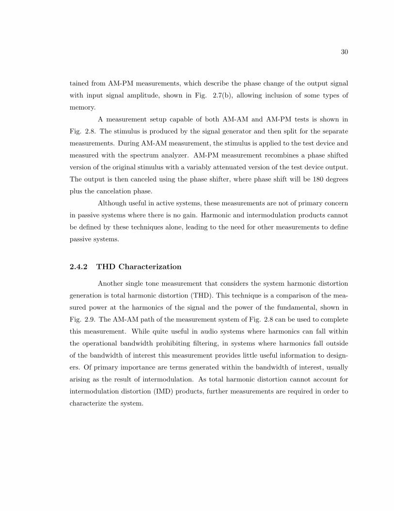
AM-AM measurements characterize the relationship between input signal ampli-
tude and output signal amplitude at the fundamental frequency, shown in Fig. 2.7(a).
AM-AM, as the name implies, only accounts for the nonlinear, memoryless amplitude char-
acteristics of a system, usually through a polynomial model. This technique is useful for
characterizing gain in active systems but lacks phase information. Phase data can be ob-
30
tained from AM-PM measurements, which describe the phase change of the output signal
with input signal amplitude, shown in Fig. 2.7(b), allowing inclusion of some types of
memory.
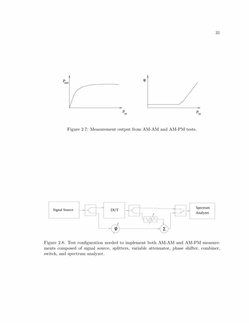
A measurement setup capable of both AM-AM and AM-PM tests is shown in
Fig. 2.8. The stimulus is produced by the signal generator and then split for the separate
measurements. During AM-AM measurement, the stimulus is applied to the test device and
measured with the spectrum analyzer. AM-PM measurement recombines a phase shifted
version of the original stimulus with a variably attenuated version of the test device output.
The output is then canceled using the phase shifter, where phase shift will be 180 degrees
plus the cancelation phase.
Although useful in active systems, these measurements are not of primary concern
in passive systems where there is no gain. Harmonic and intermodulation products cannot
be defined by these techniques alone, leading to the need for other measurements to define
passive systems.
2.4.2 THD Characterization
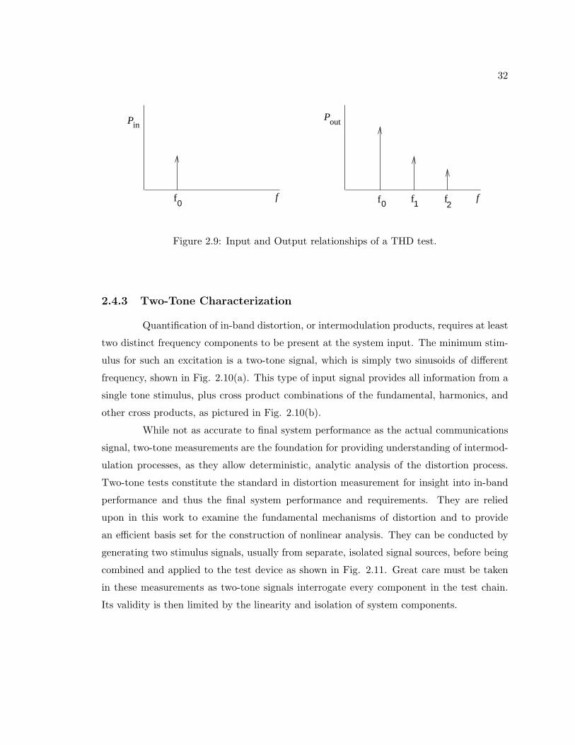
Another single tone measurement that considers the system harmonic distortion
generation is total harmonic distortion (THD). This technique is a comparison of the mea-
sured power at the harmonics of the signal and the power of the fundamental, shown in
Fig. 2.9. The AM-AM path of the measurement system of Fig. 2.8 can be used to complete
this measurement. While quite useful in audio systems where harmonics can fall within
the operational bandwidth prohibiting filtering, in systems where harmonics fall outside
of the bandwidth of interest this measurement provides little useful information to design-
ers. Of primary importance are terms generated within the bandwidth of interest, usually
arising as the result of intermodulation. As total harmonic distortion cannot account for
intermodulation distortion (IMD) products, further measurements are required in order to
characterize the system.
31
φ
P P
Pout
in in
Figure 2.7: Measurement output from AM-AM and AM-PM tests.
Signal Source DUTSpectrumAnalyzer
φ Σ
Figure 2.8: Test configuration needed to implement both AM-AM and AM-PM measure-ments composed of signal source, splitters, variable attenuator, phase shifter, combiner,switch, and spectrum analyzer.
32
0
P Poutin
f ff f f2
f10
Figure 2.9: Input and Output relationships of a THD test.
2.4.3 Two-Tone Characterization
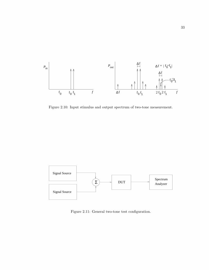
Quantification of in-band distortion, or intermodulation products, requires at least
two distinct frequency components to be present at the system input. The minimum stim-
ulus for such an excitation is a two-tone signal, which is simply two sinusoids of different
frequency, shown in Fig. 2.10(a). This type of input signal provides all information from a
single tone stimulus, plus cross product combinations of the fundamental, harmonics, and
other cross products, as pictured in Fig. 2.10(b).
While not as accurate to final system performance as the actual communications
signal, two-tone measurements are the foundation for providing understanding of intermod-
ulation processes, as they allow deterministic, analytic analysis of the distortion process.
Two-tone tests constitute the standard in distortion measurement for insight into in-band
performance and thus the final system performance and requirements. They are relied
upon in this work to examine the fundamental mechanisms of distortion and to provide
an efficient basis set for the construction of nonlinear analysis. They can be conducted by
generating two stimulus signals, usually from separate, isolated signal sources, before being
combined and applied to the test device as shown in Fig. 2.11. Great care must be taken
in these measurements as two-tone signals interrogate every component in the test chain.
Its validity is then limited by the linearity and isolation of system components.
33
20 f1 f0∆ f f1
f0 f1−∆ f | |=∆ f
∆ f
f0 f1
+f0 f1
Pin
f0 f
Pout
f2f
Figure 2.10: Input stimulus and output spectrum of two-tone measurement.
Signal Source
Signal Source
DUTΣSpectrumAnalyzer
Figure 2.11: General two-tone test configuration.
34
2.4.4 Multi-Tone and Band-Limited Continuous Characterization
Two-tone measurement techniques fail to provide information on an important
parameter in communications systems, co-channel distortion coincident with fundamentals.
Distortion components that fall on top of fundamentals affect the signal to noise ratio
of the channel, but are impossible to measure in two tone tests due to the strength of
fundamentals in comparison to the mixing products at those frequencies. Accounting for
these distortion components can be accomplished by using bandlimited continuous signals
such as pseudo-randomly digitally modulated carriers, multi-tone signals, and bandlimited
noise. Since these signals have many contributions at a given frequency, the non-correlated
intermodulation distortion at fundamentals can be determined by notch filtering of the
input signal at the intended measurement frequency. This measurement, the noise power
ratio (NPR), is unable to determine correlated intermodulation. These components can
be found through the co-channel power ratio test (CCPR) which measures both correlated
and uncorrelated intermodulation products by removing, or cancelling, the original input
stimulus at the output, bandlimited gaussian white noise. Of course the drawback of this
approach for PIM process exploration is that these signals are statistically defined, adding
considerable complexity to the mathematics of already complicated and unknown systems.
2.4.5 Passive Distortion Measurement
Application of multi-tone and even higher complexity signals seemingly give us
the most complete subset of information about the distortion processes of a system. In
active systems, the knowledge of nonlinear co-channel contributions, both correlated and
uncorrelated, is needed for correct operation and design of the system. Passive systems
are not strongly nonlinear as in the active case, lessening the need for knowledge of in-
band distortion coincident with fundamentals. More important are the intermodulation
products, which can fall in receive bands causing interference leading to degradation of
signal to noise ratios and possibly even blocking communication channels. Due to the
general lack of knowledge as to what the processes are that produce distortion in passive
devices, a deterministic, mathematically tractable signal that provides mixing products is
an ideal test candidate. Two-tone testing provides exactly this tractable analysis of test
results. It is used throughout this work in order to analyze the physical processes associated
35
with passive distortion. Unfortunately, measurement of passive distortion is virtually never
as simple as application of two tones to a passive device, as passive processes produce such
weak distortion that the dynamic range requirements become intensive.
Passive components are often so weakly nonlinear that the distortion they produce
is immeasurable by conventional systems even at several watts of input power to the passive
device, due to the extremely large magnitude of the probe stimuli [44]. The output of
these devices must be pre-conditioned in some manner in order for spectrum analyzers or
vector signal analyzers to be able to measure the products of interest without generating
their own distortion, masking the intermodulation signals. This pre-conditioning must
necessarily accomplish the reduction of the probe stimuli magnitude while not affecting the
desired distortion products. Attenuation could be introduced to reduce or eliminate receiver
nonlinearity, but this will both reduce the magnitude of nonlinearities and increase noise.
Reducing both noise and carrier level simultaneously to provide the dynamic range needed
for passive distortion measurement requires filtering or active feed-forward techniques [45].
Filter Based Methods
Bandpass filtering is normally applied to RF systems in order to remove harmonics
from the system. Application of filters to intermodulation measurement is usually limited
by the small frequency separation of the IMD products from the fundamental signals. High
order duplexers can help bypass this issue, as high isolation and tight separation of fre-
quency bands can be obtained. Proper choice of probing stimuli frequencies can allow
the intermodulation products to fall within the receive band of the duplexer. Commercial
systems have reported dynamic ranges of 168 dBc in two-tone tests at 20 Watts per car-
rier [14]. Although these systems present amazing dynamic range, they are limited by their
lack of tunability. High isolation from high order filters requires signals to be fixed within
the filter bandwidths, leading to very narrow band systems limited to several megahertz
tone separations. Many processes have thermal dependencies, which are always dependent
on amplitude modulation of a signal. As input stimuli are brought increasingly close in
frequency to each other, amplitude modulation increases, thereby characterizing those pro-
cesses. Filtering based systems cannot measure such a variation and are thus fundamentally
limited in exploring any PIM process with a wide band frequency or thermal dependence.
36
Figure 2.12: Cancelation as a function of phase and amplitude error between original andcanceling tone.
Feed-Forward Techniques
Passive process characterization requires the measurement of at least two-tone
signals over wide, tunable bandwidths with massive dynamic range and many variations
of frequency separation. These requirements are competing in any filtering based method,
leading to the need for a technique not reliant on filtering. Harold Black [46], the inventor of
feedback in circuits, supplied this method with the advent of feed-forward techniques. Feed-
forward is an unconditionally stable technique, thus is inherently broadband. Feed-forward
relies on the cancelation of signals at a reference plane by combining the undesired signal
with an amplitude matched version of the same signal with opposite phase and equal delay.
Cancelation can be thought of as the vector addition of two signals resulting in destructive
interference of the signal [46].
Knowledge of many things are needed to perform cancelation including exact am-
plitude and phase of the signal to be canceled as well as the loss and delay of the channel
37
Signal Source
Signal Source
Σ DUT ΣSpectrumAnalyzer
φ
φ
Figure 2.13: General feed-forward system measurement architecture.
over frequency. The stringency of this requirement lies in the statement of exact amplitude
and phase. In any real system there will be some degree of error in both the amplitude
and phase measurements. The deviation from ideal cancelation due to amplitude and phase
error follows the well known equation for rejection,
PO − PC = −10 log(α2 + 2α cos (φ) + 1
)(2.8)
Where Po − Pc is the difference in amplitude (dB) of the original signal and the canceled
signal. The α and φ terms represent the amplitude and phase error, respectively. A contour
plot is shown in Fig. 2.12 of cancelation versus phase and amplitude error clearly showing
that very small errors result in large deviations from ideal cancelation. Schemes such as
power minimization and gradient techniques are effective at canceling tones even under such
high accuracy requirements because they iterate towards the true value through an error
function instead of requiring exact values for amplitude and phase. These methods often
take many iterations to reach reasonable cancelation levels [45].
As long as the signals are continuous wave and not containing transient compo-
nents, the delay associated with cancelation can be tolerated in order to gain virtually
unlimited bandwidths and tone separations. If transient signals are to be measured, cance-
lation for PIM measurement cannot be used unless periodically pulsed signals are used to
determine cancelation parameters a priori to the cancelation or the signal operates much
slower than the cancelation control loop. If all these requirements are met, this technique
is very attractive for high dynamic range measurements.
38
20 f1 f0∆ f f1
f0 f1−∆ f | |=
∆ f
f0 f1
+f0 f1∆ f
Pin
f0 f
Pout
f2f
Figure 2.14: Input and output spectrum of feed-forward measurement system.
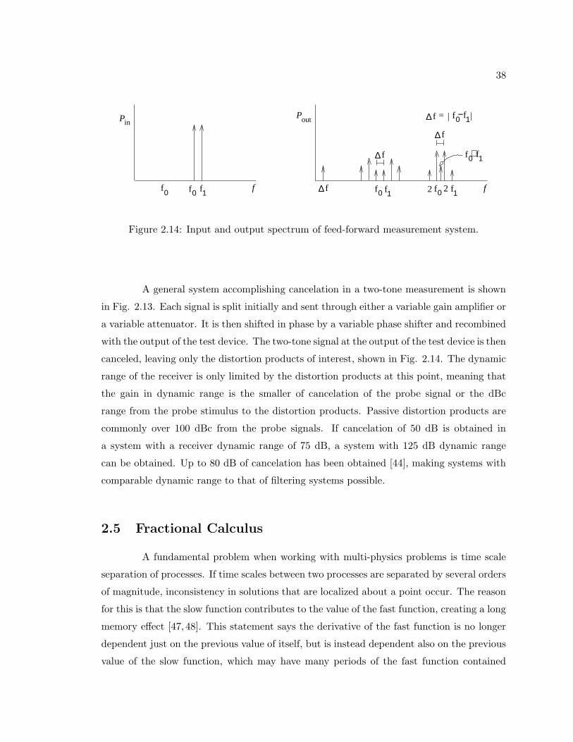
A general system accomplishing cancelation in a two-tone measurement is shown
in Fig. 2.13. Each signal is split initially and sent through either a variable gain amplifier or
a variable attenuator. It is then shifted in phase by a variable phase shifter and recombined
with the output of the test device. The two-tone signal at the output of the test device is then
canceled, leaving only the distortion products of interest, shown in Fig. 2.14. The dynamic
range of the receiver is only limited by the distortion products at this point, meaning that
the gain in dynamic range is the smaller of cancelation of the probe signal or the dBc
range from the probe stimulus to the distortion products. Passive distortion products are
commonly over 100 dBc from the probe signals. If cancelation of 50 dB is obtained in
a system with a receiver dynamic range of 75 dB, a system with 125 dB dynamic range
can be obtained. Up to 80 dB of cancelation has been obtained [44], making systems with
comparable dynamic range to that of filtering systems possible.
2.5 Fractional Calculus
A fundamental problem when working with multi-physics problems is time scale
separation of processes. If time scales between two processes are separated by several orders
of magnitude, inconsistency in solutions that are localized about a point occur. The reason
for this is that the slow function contributes to the value of the fast function, creating a long
memory effect [47, 48]. This statement says the derivative of the fast function is no longer
dependent just on the previous value of itself, but is instead dependent also on the previous
value of the slow function, which may have many periods of the fast function contained
39
within it. In most physical cases, the fast process is not coupled to the slow process as
it will average to zero before a change in the slow function can occur [48]. However, in
multi-physics situations where diffusion processes or diffusion equations are involved, the
faster wave process can be tangibly affected by the slower diffuse process, provided that
the fast process has appreciable variation within the bandwidth of the slower process. The
result of time scale inseparability and long memory is the need to recast the system as a
fractional differential equation.
The fractional derivative is a non-local operator that embeds the complete knowl-
edge of the past history of a function [47–51]. Due to this property, it is possible to create
physically based reduced order models of phenomena that could not be conveniently de-
scribed by integer order models. It is exactly this property that makes them so useful. By
recasting a partial differential equation as a fractional equation, not only can a reduced
order model be obtained, but since the fractional solution contains memory of the entire
function it also alleviates the need to solve the entire spatial domain. This property ef-
fectively reduces the partial differential equation for any chosen point to a function only
dependent on time while still accounting for spatial effects throughout the entire medium.
For the equation to be recast as fractional, either an equation can be suggested or the
equation can be derived from integer order constitutive equations. The main drawback for
the use of fractional calculus is its complexity in implementation, specifically as it applies
to commercial simulators. Although there are several ways to circumvent these problems,
only extremely limited implementations currently exist.
2.5.1 Fractional Calculus Natural Functions
In any branch of mathematics, a few functions with special properties exist that
allow them to be used for the solution of many problems with fractional calculus descrip-
tions. An example of this statement are the transcendental functions and the exponential.
Their special properties allow them to be used as a basis set to approximate an incredi-
bly large group of functions and solve an incredibly large group of problems. Several of
these functions exist in the fractional calculus as well, the most important of which are the
gamma, beta, and Mittag-Leffler functions.
40
Gamma Function
The gamma function was developed by Euler in order to generalize the factorial
to all real numbers. It can take the form of an integral and is given by
Γ (t) =
∞∫
0
e−xxt−1dx. (2.9)
where t can be a complex number. Several important properties are exhibited by this
function. When t is positive real, the gamma function can be expressed as
Γ (t) = (t− 1)!, (2.10)
and for all real numbers
Γ (t + 1) = tΓ (t) . (2.11)
These relationships allow the extension of the gamma function to negative real numbers.
Interestingly, the function goes to infinity at negative integer values but is defined for
negative non-integer values [49–51].
Beta Function
The Euler beta function is important in fractional calculus due to its similar form to
the fractional integrals and derivatives of many polynomials and the Mittag-Leffler function.
The function is conveniently given in terms of the gamma function by
B (x, y) =
1∫
0
(1− t)y−1 tx−1dt =Γ (x) Γ (y)Γ (x + y)
, (2.12)
where x and y are positive real.
Mittag-Leffler Function
The exponential function is often used to solve integer order differential equations
and may be considered a natural solution to those equations. The fractional analog of a
natural solution is the Mittag-Leffler function [49–51] which is represented by
41
Eα,β (x) =∞∑
k=0
xk
Γ (αk + β), (2.13)
where α and β are complex parameters, but the real part of α is restricted to be positive. It is
interesting to note that the Mittag-Leffler function contains several other natural functions
within it, depending on the values chosen for α and β, including the exponential function,
error function, the sum of a geometric progression, and hyperbolic trigonometric functions.
The Mittag-Leffler functions interpolate between a purely exponential law and power-like
behavior of phenomena, and are natural solutions to random walks, Levy flights, and many
more fractional processes [47,48].
2.5.2 Fractional Integral Definition
The fractional integral form most often used is that of Riemann-Liouville. They
sought to extend the integer order integral through the use of the Cauchy formula for
repeated integration. This formula gives the nth integration of a function,
f [n] (t) =
t∫
0
y1∫
0
· · ·yn−1∫
0
f (yn)dyn · · · dy2dy1 =1
(n− 1)!
t∫
0
(t− τ)n−1 f (τ)dτ. (2.14)
The factorial function in (2.14) restricts n to integer integrations. To reach a fractional
integration, the factorial can be expanded for all real numbers, resulting in the gamma
function. The fractional integral becomes
fa (t) =1
Γ (a)
t∫
0
(t− τ)a−1 f (τ)dτ, (2.15)
where α can now be any positive real number. It should be noted that the effect of the
integration limit at zero forces the causality of the function [49–51].
The fractional integral can also be derived in a different manner, used by Grunwald
and Letnikov. In this definition, instead of repeated integration, repeated differentiation
was first defined and then extended to negative order fractional exponents [49]. The result
is an equivalent formation to the Riemann-Liouville definition, given by
d−αf (t) = limh→0
hα
t−hα∑
m=0
Γ (α + m)m!Γ (α)
f (t−mh) . (2.16)
42
2.5.3 Fractional Derivative Definition
Fractional Calculus has had many contributors, each with their own definition
of the fractional derivative and integral. The three most relevant definitions, Riemann-
Liouville, Caputo, and Grunwald-Letnikov are briefly reviewed here along with the laplace
representation of a fractional derivative or integral.
Riemann-Liouville Definition
In Newton’s classical calculus, Cauchy reduced the calculation of an n-fold integral
of the function f(t) into a single convolution integral possessing an Abel power law kernel.
Riemann and Liouville continued his work to develop perhaps the most well known definition
of the fractional derivative which is given by:
aDpt f(t) =
(d
dt
)m+1t∫
a
(t− τ)m−p f(τ)dτ, (m ≤ p < m + 1). (2.17)
The concept behind this definition of the fractional derivative is the use of frac-
tional integral first, followed by the subsequent integer order differentiation. This definition
is preferable in the mathematical community for the explicit reason of the order of these
operations. Since integration is the first operation, as long as the function meets the con-
dition of causality, so must all the subsequent derivatives. While this is a great feature
mathematically, it results in the need for fractional derivative initial conditions in order to
solve real world problems [49–51].
Caputo Definition
In engineering, initial conditions must be specified in terms that are physically
definable. To solve this practical need, M. Caputo redefined the Riemann-Liouville ap-
proach to the fractional derivative by reversing the order of operations. In his definition,
differentiation of integer order is performed first, followed by subsequent fractional order in-
tegration using the same approach as Riemann and Liouville. His definition of the fractional
43
derivative is given by:
Ca Da
t f(t) =1
Γ(a− n)
t∫
a
f (n)(τ)(t− τ)a+1−n dτ, (n− 1 ≤ a < n). (2.18)
Caputo’s definition, unlike the Riemann-Liouville definition, can use standard in-
teger order derivatives as initial conditions, which are physically defined. The derivative of
a constant using Caputo’s definition is zero, unlike the Riemann-Liouville definition, which
provides a non-zero result. In essence, the Caputo definition allows application of fractional
calculus to real problems [49–51].
Grunwald-Letnikov Definition
Unlike the Riemann-Liouville and Caputo definitions of the fractional derivative,
the Grunwald-Letnikov definition does not focus on a repeated integration, but instead
focuses on repeated differentiation [51]. Starting with the definition of the derivative,
f ′(x) = limh→0
f(x + h)− f(x)h
, (2.19)
and applying the formula a second time to obtain the second derivative:
f ′′(x) = limh→0
f ′(x + h)− f ′(x)h
= limh1→0
limh2→0
f(x+h1+h2)−f(x+h1)
h2 −lim
h2→0f(x+h2)−f(x)
h2
h1(2.20)
f ′′(x) = limh→0
f(x + 2h)− 2f(x + h) + f(x)h2
. (2.21)
For an nth-order derivative, the formula is reduced to Grunwald’s definition when
the binomial sum is expanded to fractional values using the gamma function. The Grunwald-
Letnikov definition of the fractional derivative is thus given by
Dnt0f(t) = lim
h→0
1hn
t−t0h∑
j=0
(−1)j(nj
)f(t− jh)
= limh→0
1hn
t−t0h∑
j=0
(−1)j Γ(a + 1)j!Γ(a− j + 1)
f(t− jh).
(2.22)
The importance of the Grunwald-Letnikov definition, as can be seen, is the fact that it lends
itself to direct numerical approximation of the derivative of any order.
44
Fractional Laplace and Fourier Transform
The laplace transform is a powerful solution method for differential equations as
it allows transformation of the equation to an algebraic equation of the transform variable.
This technique can be used in certain situations to eliminate either space or time dependen-
cies in a partial differential equation, turning it into a solvable ordinary differential equation
in the other variable. The laplace transform is quite well known and widely used for engi-
neers working in the frequency domain, alongside the fourier transform. Representation of
the fractional derivative and integral in the frequency domain can be accomplished through
the generalization of the laplace transform to fractional orders.
The premise of the proof of the fractional laplace transform is the equivalence of
a convolution kernel in the time domain to its constituent pieces multiplied in the laplace
domain [51]. The laplace convolution kernel is given by
f (t) ∗ g (t) =
t∫
0
f (t− τ) g (τ)dτ. (2.23)
Now define a function
Φα (x) =xα−1
Γ (α), (2.24)
and convolve that function with an arbitrary function f (x) to yield
Φα (x) ∗ f (x) =
t∫
0
(x− t)α−1
Γ (α)f (t)dt, (2.25)
which is in fact the fractional integral. The laplace transform of Φα (x) is quite simple by
choice, and is given by
L
xα−1
Γ (α)
= s−α. (2.26)
Multiplying the respective transforms, the equivalent of the fractional integral in the laplace
domain is obtained, which is
L
dt−α
dτ−αf (x)
= s−αf (s) . (2.27)
Since fractional differentiation can always be performed by a fractional integral and separate
integer order derivative, this formula is easily extended to the fractional derivative, resulting
45
in
L
dtα
dταf (x)
= sαf (s) . (2.28)
Although a proof could also be extended to fourier analysis, the relationship between the
fourier variable ω and the laplace variable s allows direct translation to the fourier domain.
2.5.4 Fractional Differential Equations
Wave and diffusive behavior are not as separate as would be preferable from a
mathematical standpoint. An example of this fact is low frequency electromagnetic in-
duction. At low frequencies the system acts diffusively, but as the frequency is increased,
behavior becomes blended between wave and diffusive behavior before it finally transitions
to primarily wave behavior.
In terms of the constituent partial differential equations, this means that the order
of the equation lies some where between a first and second order process (1 < α < 2) imply-
ing a blending of oscillatory and relaxation processes. Diffusion processes are often better
represented by fractional systems of less than order one, (0 < α < 1). Using multiple frac-
tional derivatives of various order can include any combination of system behavior desired,
making it one of the most versatile mathematical methods available to the engineer. The
solutions of these equations follow similar methods to that of integer order equations, but
using fractional versions of the methods instead such as the fractional laplace transform or
adapted green’s functions.
2.5.5 Numerical Methods
Even if analytic solution to a problem is possible, it is usually simplified to an
extent. Although it provides great intuition to designers, extremely accurate simulations
are inevitably needed to create reliable products. In order to simulate these problems
quickly and accurately, application of fractional differential equations is paramount. The
long memory requirement of fractional solutions has hampered its adoption by making
time domain implementation difficult, which is needed for nonlinear simulation. Several
methods have been developed, and continue to be developed, to alleviate this concern.
46
Several methods of interest are reviewed here, including the short memory principle, the
time scaled method, and memory-less methods.
Short Memory Principle
The short memory principle was introduced by Igor Podlubny to shorten the large
amounts of memory needed to compute fractional derivatives [51]. In looking at the original
Grunwald-Letnikov definition that for large times, the role of the history of the behavior of
the function becomes negligible near the lower terminal t = a under certain conditions. He
prescribes taking into account only the most recent history of the function, in the interval
[t− L, t], where L is the memory length:
aDαt f(t) ≈t−L Dα
t f(t), (t > a + L). (2.29)
The derivative is approximated at the lower terminal by a moving lower terminal. The error
estimate for this simplification is given by:
∆(t) = |aDαt f(t)−t−L Dα
t f(t)| ≤ ML−α
|Γ(1− α)| , (a + L ≤ t ≤ b). (2.30)
If the desired accuracy (ε ) is known, it can be used to determine the required memory
length, given by
∆(t) ≤ ε → L ≥(
M
ε|Γ(1− α)|)1/α
. (2.31)
Time Scaled Method
All of the aforementioned methods for implementing the fractional derivative have,
to a degree, lacked a clear time domain representation. In [52] the authors propose a
time scaled method of differentiation. In their interpretation, a discrete fractional order
derivative is the derivative of the sampling time scaled discrete integral. The Riemann-
Liouville definition of the derivative is rewritten to yield
0Dat f(t) =
1Γ(1− a)
d
dt
t∫
0
f(τ)[t− τ ]a
dτ =d
[t∫0
f(τ)dg′t(τ)
]
dt, (2.32)
47
with the integration factor rewritten as a derivative, which is given by
g′t(τ) =
1Γ(2− a)
[t1−a − (t− τ)1−a
]. (2.33)
The scaled sampling time steps are given by:
T′n(n) =
11−a − 01−a
Γ(2− a)T 1−a (2.34)
T′n(n− 1) =
21−a − 11−a
Γ(2− a)T 1−a (2.35)
T′n(1) =
n1−a − (n− 1)1−a
Γ(2− a)T 1−a, (2.36)
where Tn is the sampling time at the nth time step and a is the order of the derivative.
Finally, application of the trapezoidal integration rule yields
nT∫
0
f(τ)dg′t(τ) ≈
n∑
k=1
f(kT ) + f [(k − 1)T ]2
T′n(k), (2.37)
where T is the constant time step. According to the authors [38,46], the interpretation of
discrete fractional order derivatives are the derivatives of fractional (1− α) order integrals.
It can be understood geometrically as the changing ratio of the “scaled integral area” due
to the scaled sampling time.
Memoryless Fractional Derivatives
Very recently, Yuan and Agrawal [53, 54] proposed a method for evaluating frac-
tional derivatives that requires no storage and processing of the function history. This
method is based on a transformation of the fractional differential equation to a set of ordi-
nary integer order differential equations. In internal variable theory equivalence between an
exponential kernel and an ordinary linear differential equation can be drawn, just as with
fractional derivatives. They consider a general fractional differential equation of the form,
mD2x (t) + cDαx (t) + kx (t) = f (t) (2.38)
48
with the derivative defined as the Riemann-Liouville fractional derivative. Noting the
gamma function properties
Dax(t) =
t∫
0
(t− τ)−a
Γ(1− a)Dx(τ)dτ (2.39)
Γ(a) =
∞∫
0
e−zta−1dz (2.40)
Γ(a)Γ(1− a) =π
sin(πa), (2.41)
The fractional derivative can be rewritten as
Dax(t) =sin(πa)
π
t∫
0
∞∫
0
e−z
[z
t− τ
]a dz
z
Dx(τ)dτ. (2.42)
Substituting z = (t− τ)y2 and rewriting the derivative,
Dax(t) =2 sin(πa)
π
∞∫
0
y2a−1
t∫
0
e−(t−τ)y2Dx(τ)dτ
dy, (2.43)
as well as introducing the new variable
φ(y, t) = y2a−1
t∫
0
e−(t−τ)y2Dx(τ)dτ (2.44)
allows the fractional differential equation to be written, upon taking the time derivative, as
Dφ(y, t) + y2φ(y, t) = y2a−1Dx(t). (2.45)
This formulation allows the fractional differential equation to be solved without function
history. Only integration of the remaining integer order equation is required.
Summary of Fractional Calculus
Several numerical methods to compute the fractional derivative, used to reduce the
requirement of full function memory at every time step, were reviewed in this Section. The
49
short memory principle simply truncates the memory of the fractional derivative computa-
tion to a length that causes a pre-determined, user defined amount of error. The time scaled
method uses standard trapezoidal integration, but varies the time step of the integration to
represent a fractional derivative. This property makes it attractive for implementation into
circuit simulators with variable time step capabilities. The memoryless method is ideal for
implementation in standard circuit simulators, as it allows a fractional differential equation
to be recast into an integer order equation that can be solved with standard numerical
integration methods. This review was conducted to allow further implementation of the
work in this dissertation. No reduction in complexity using numerical methods was used
in this work. Fractional derivatives were numerically computed using the definition of the
Grunwald-Letnikov and Caputo fractional derivative definitions.
2.6 Conclusion
Passive components such as resistors, transmission lines, and antennas can pro-
duce intermodulation distortion under high power input conditions, which is referred to as
passive intermodulation distortion. PIM is generally a much weaker nonlinearity than the
nonlinearity of active components such as amplifiers. The weakness of the linearity coupled
with the large number of potential nonlinear mechanisms has made physical description of
PIM difficult. Many physical mechanisms have been suggested as the cause of PIM, in-
cluding metal-oxide-metal and metal-metal contacts, ferromagnetic materials, piezoelectric
materials, acoustic coupling, and electrical conductivity modulation. Each mechanism was
reviewed in this Chapter to allow separation of the mechanisms in this work. The differ-
ences in material properties favored electrical conductivity modulation as a dominant PIM
mechanism as it must exist in every microwave component.
Several of the PIM generating mechanisms often exist concurrently in microwave
devices, limiting the modeling of passive devices to empirical or behavioral models. A review
of common distortion analysis and modeling techniques was given including the power series
and volterra series. The differences between behavioral modeling and physical models were
discussed, with an emphasis on the design benefits of a physical model compared to empirical
or behavioral techniques.
50
Passive intermodulation distortion was described as a weak nonlinearity requiring
high dynamic range measurement methods for analysis. Common distortion characteriza-
tion methods such as AM-AM, AM-PM, total harmonic distortion, two-tone, and multi-tone
were reviewed. Two-tone measurements were shown to be the most useful method for this
work, as they allow the most simple analytic formulations of PIM. Measurement systems
and methods capable of the high dynamic range necessary for PIM testing were reviewed.
Although the highest dynamic range is obtained by filter based methods, the system does
not allow the test frequencies and separations to be varied substantially. Feed-forward
cancellation was shown to be the most relevant measurement method for this work.
A short review of fractional calculus was conducted to allow the modeling of
electro-thermal distortion in this dissertation. The definitions used to compute long-tail
transients and frequency responses, as well as derive analytic electro-thermal physics were
provided. Numerical methods that can be used to reduce the computational complexity of
fractional derivatives were presented to allow future expansion of this work into standard
circuit simulators.
51
3
Broadband High Dynamic Range
Measurement
52
3.1 Introduction
Intermodulation distortion can be the limiting factor in high dynamic range com-
munication systems such as satellites and cellular basestations. Although the active system
components are designed to meet an industry distortion specification, often passive com-
ponents such as transmission lines, filters, combiners, and antennas in the transmit path
produce distortion after the active components which can then couple to the receive sys-
tem. Two-tone testing is conventionally used to characterize and identify the sources of
nonlinear distortion. This requires the ability to measure distortion components that could
be 100 decibels or more below the level of applied tones and separated by a few hertz.
Measurements of tones separated by a few hertz is required to distinguish between sources
of passive intermodulation distortion (PIM), specifically electro-thermal PIM, nonlinear
junction effects, and tunneling [55,56].
In a nonlinear distortion measurement systems, large stimulus tones are applied to
the device under test (DUT), and nonlinear distortion components are generated at much
lower power levels. The interfering stimulus must be removed before reaching the receiver,
as distortion signals would otherwise be masked by distortion generated in the receiver [57].
To reduce both the stimulus signal and large noise levels simultaneously, filtering or active
feed-forward techniques [58] are needed.
High dynamic range measurement systems based on filtering typically use diplexers
or notch filters to remove system-generated distortion components before application to the
DUT. A second filtering stage removes the stimulus signal before final measurement of the
distortion components by a spectrum or vector analyzer [14]. This scheme has the highest
dynamic range but cannot be used with closely spaced tones because of the limited roll-off
of the filter skirts. Overcoming tunability limitations is of utmost importance when testing
for passive intermodulation distortion (PIM), as some types of PIM such as electro-thermal
distortion must be tested for at very small tone separations where no filter skirt can be
sharp enough. The only choice for broadband, spacing independent distortion testing is
feed-forward cancellation.
Feed-forward cancellation directly increases the dynamic range of the system by
the cancellation achievable until the components of the test system itself begin to generate
distortion. Every component will produce PIM at some level, generally dependent on both
53
power and frequency. Active devices, even if confined to a single frequency, will produce
spurious frequency content at PIM frequencies if there is a radiation path in the system.
Reflections and finite isolation in the system compound the nonlinearities due to forward and
backward wave mixing in components that should be single frequency. All of these effects
must be accounted for in order to provide high dynamic range measurement capabilities.
This chapter details the design and test of a high dynamic range measurement
system based on feed-forward cancellation. Feed-forward theory and system design concepts
are discussed in Section 3.2 and Section 3.3. Component linearity for each type of component
used in the system is discussed in Section 3.4. Design concepts for high dynamic range
included reflection effects, load matching, limiting amplifier mixing, and radiative coupling
are presented in Section 3.5. Section 3.6 discusses system applications and performance for
two-tone PIM measurement and digitally modulated signals. Section 3.7 summarizes the
results presented in this chapter.
3.2 Feed-Forward Cancellation Theory
The process of cancelling a signal is mathematically a simple one, requiring only the
summation of that signal with an equal amplitude anti-phase signal at the same frequency.
Non-idealities such as small imbalances in amplitude, phase, and group delay must be
considered in any system implementation [59–62]. Amplitude and phase imbalance, α and
∆φ, respectively, limit the depth of cancellation achievable, while group delay imbalance
limits both the depth and bandwidth of cancellation [59–63]. Cancellation performance,
CP, is described by
CP = 10 log(
1 + α2 − 2α cos(
2π ·∆λ
(1− f
fc
)+ ∆φ
)), (3.1)
where ∆λ is the difference in wavelengths between the two paths normalized to the wave-
length of the center frequency, fc, and f is the frequency of operation. Group delay mis-
match affects bandwidth due to the deviation of phase shift of the cancellation and signal
paths as the frequency is shifted away from the center frequency of cancellation. The limit-
ing effect of group delay on the cancellation depth results from the degree of delay mismatch.
As the difference in delay grows, so does the rate of phase mismatch with increasing sep-
aration from the center frequency. Group delay can be matched to a level acceptable for
54
0 20 40 60 80 100 120 140 160 180−140
−120
−100
−80
−60
−40
−20
−S
igna
l Can
cella
tion
(dB
)
Phase Difference, φ, (deg)
−0.2
0
0.2
0.4
0.6
0.8
1
1.2
Pha
se P
redi
ctio
n E
rror
(de
g)
Figure 3.1: Predicted phase shift error of (3.8) versus actual phase difference between theoriginal signal and the cancellation signal from 0 − 180. Also shown is the cancellationachievable with (3.8) if the amplitude of the original and canllation signal are the same.
bandwidth requirements according to (3.1). Under these conditions, the phase shift and
amplitude necessary for cancellation must be obtained. The method developed here auto-
matically tunes the center frequency of the cancellation signal enabling the measurement
system to operate over wide bandwidths.
Cancellation methods using power minimization or gradient techniques are effec-
tive at eliminating phase error iteratively, but the number of iterations to reach cancellation
in excess of 30 dB can be large [58,62,64]. In the work described here a formula is used to
determine the phase shift necessary for cancellation given the amplitude of the combined
feed-forward and DUT signal, resulting in greater speed and accuracy than can be obtained
with iterative search methods. Amplitude matching is described after discussion of phase
correction. The formula is based on amplitude measurements facilitating implementation
using standard laboratory equipment such as a spectrum analyzer, an oscilloscope, or a
vector signal analyzer. Development of a formula based on amplitude measurement can be
55
obtained by first considering the cancellation of a single sinusoidal signal.
Consider a single sinusoidal signal which is the combination of the original signal
and the cancellation signal [65],
α cos (ω1t + φ1) + α cos (ω1t + φ2) = β cos (ω1t + φ3) (3.2)
where α is the amplitude of both the original and cancellation signal, ω1 is the radian
frequency of the signals, φ1 is the phase of the original signal, φ2 is the phase of the
cancellation signal, φ3 is the combined signal phase, and β is the combined signal amplitude.
Since the tones are at the same frequency, this can be rewritten as a function of only the
magnitude and phase difference,
cos (φ1) + cos (φ2) =β
α, (3.3)
which can be seen by setting φ3 = 0 and considering t = 0 in (3.2). From trigonometric
identities it can be shown that
cos (φ1) + cos (φ2) 2 cos(
φ1 + φ2
2
)cos
(φ1 − φ2
2
). (3.4)
The phase of the combined signal is related to the phase of the cancellation and original
signal by
(φ1 + φ2)2
= φ3 = 0. (3.5)
Defining φ1 − φ2 as the phase difference φ, (3.3) and (3.4) become
cos(
φ
2
)=
β
2α. (3.6)
Solving for the phase difference gives
φ = nπ ± 2 arccos(
β
2α
); n = 0, 1, ... . (3.7)
The phase difference required for cancellation is π. Choosing n = 0 and rewriting in terms
of the phase shift required for complete cancellation, φs [65],
φs = π ± 2 arccos(
β
2α
). (3.8)
There will be a phase prediction error, in general, which is the difference between
the predicted phase shift and the ideal phase shift. This error tends to reduce as the signals
56
approach 180 phase difference. This can be seen in Fig. 3.1, where the signal cancellation
achieved for equal amplitude signals is plotted versus signal phase difference. The absolute
phase error of the formula is also shown against phase difference in Fig. 3.1. The accuracy
of the formula, assuming no amplitude error, is lowest when the two tones have a phase
difference of 3. At this point the formula has 1.242 of phase error, which limits cancellation
to 33 dB. Error reduces as the phase difference of the tones increases, lending itself to greatly
increased accuracy upon a second application, in practice often exceeding 50 dB. Although
the formula is derived to cancel only a single tone, it is extensible to other signals such as
digital modulation and multi-sine, where the cancellation bandwidth can be derived from
(3.1).
Equation (3.8) provides only the magnitude of the required phase shift. Thus
taking one of the solutions, say the positive phase shift, may not increase cancellation
and so the negative phase shift must then be used. With a vector signal analyzer used
to measure both the phase and amplitude of the signal component being cancelled, it is
possible to determine which phase shift solution to use. Implementation of (3.8) can be
accomplished through the establishment of a reference cancellation plane. The reference
plane is established by measuring the probe tone power and then measuring the power
from the combination of the feed-forward path and the DUT path signals at the bridge
point. Their respective phases must also be measured if the sign of the phase shift is to
be determined. Only two amplitude measurements are required to determine where the
relative phase of the tones is on the unit circle before cancelling those tones.
The DUT signal amplitude is matched automatically at the bridge point using
feed-forward path amplitude calibration. The system of Fig. 3.2 automatically calibrates
the feed-forward channel transmission characteristic to extract measurement error, channel
losses, and vector modulator characteristics. The calibration is used to generate an output
power characteristic as a function of power and frequency to enable amplitude correction
between the system DUT and feed-forward paths.
57
DUT Path
Split
ter
Isolator
Combiner
Isolator
DUTPower
Amplifier
DA
CD
AC
LO
LO
Feedforward Path
o90
o0
o90
o0
0
0
IN
0
0
IN
VectorSignalAnalyzer
Digitally ControlledVector Modulator
Ref
eren
ce O
scill
ator
RF
Phas
e L
ocke
d Sy
nthe
size
r
Lim
iting
Am
plif
ier
Isol
ator
Σ
Σ
Σ
Σ
Σ
Figure 3.2: High dynamic range passive intermodulation distortion measurement systemcomposed of highly linear amplifiers, RF sources, isolators, combiners, vector modulators,and a vector signal analyzer. Four separate digital to analog converters (DACs), repre-sented by one DAC, are used to individually control the positive and negative in-phase andquadrature inputs of the vector modulators, shown with their internal schematics. The LOinput of the vector modulators is identified.
58
3.3 Linear Feed-Forward System Design
Feed-foward cancellation is an application of the bridge method for measuring
small variations in signals [66]. Typically the feed-forward and DUT paths of the bridge
combine at a reference plane. Only the original signal will be fed forward and cancelled,
enabling high dynamic range measurement of the unaffected distortion components beyond
the reference plane. A few practical issues arise that govern the implementation of the
bridge technique including phase tracking of the cancellation signal and noise coherence.
Both noise coherence and phase tracking are governed by the method used to generate the
feed-forward signal. The most prominent methods include separate sources, sampling and
regenerating the signal with analog to digital and digital to analog converters, and coupling
off of part of the original signal, are discussed in this section in the context of measurement
system architecture.
Phase instability is an unavoidable issue when employing separate cancellation
sources. Modern frequency synthesizer architectures are frequency locked rather than being
phase locked [67]. With frequency-locked sources, random phase variations of independent
fractional synthesizers are only required to have on average a particular time-varying phase
relationship. While this significantly reduces the level of spurious tones, this time-varying
phase relationship causes the phase difference between two frequency locked signals to wan-
der. Using separate sources to provide the cancellation signals thus requires constant phase
control to retain cancellation [65]. If continuous phase control is not employed, the result
is typically a slow variation of a few decibels or complete loss of cancellation. Designs that
sample or couple the original signal and use this to form the cancellation signal do not have
this phase instability problem as the cancellation signal is inherently phase and frequency
locked to the original signal.
Noise coherence only exists when coupling of the original signal is used. When
separate sources are used, the noise in the cancellation signal is random with respect to the
noise in the applied DUT signal. The noise from a sampled and regenerated signal is random
with respect to the DUT channel unless the circuitry can sample both the noise and signal.
The signals may be frequency and phase locked, but the noise will be independent and
will sum. Noise summation detracts from the dynamic range of the system, and ultimately
limits the capability of the measurement system. Feeding forward part of the original signal
59
0 50 100 150 200 250 300 350−35
−30
−25
−20
−15
−10
Phase (deg)
RF
Out
put P
ower
(dB
m)
P in
= −45 dBm
P in
= −5 dBm
(a)
0 0.2 0.4 0.6 0.8−50
−40
−30
−20
−10
0
10
I/Q Voltage (V)
RF
Out
put P
ower
(dB
m)
I CHQ CH
P in
= −5 dBm
inP = −30 dBm
(b)
Figure 3.3: Measured vector modulator response: (a) I/Q gains versus input LO drive powerbelow specification at −30 dBm and −25 dBm, and within specification at −5 dBm; and(b) output power variation with output phase over input LO drive power from −45 dBmto −20 dBm in 5 dBm increments.
60
avoids this problem, as source noise is also fed forward and cancelled, leaving only the noise
added by components such as the DUT, active devices, and passive components.
A high dynamic range feed-forward measurement system coupling off part of the
original signal is shown in Fig. 3.2. Here the system is implemented for a two-tone sig-
nal, with vector modulators used to control the phase and amplitude of the signals in the
cancellation channels replacing variable attenuators and delay lines. In the implementation
described, the Hittite HMC497LP4 vector modulators have a bandwidth of 3.9 GHz, en-
abling nonlinear vector signal analysis from 100 MHz to 4 GHz. They are digitally-controlled
by digital to analog converters (DACs) and provide up to 360 degrees phase rotation and
amplitude control between 20 and 40 dB. Isolators are used to limit the reverse traveling
waves in the system. The two branches of the bridge, the cancellation channel and DUT
channel, are finally summed at a reference plane before measurement by the vector signal
analyzer.
Reflected signals must be minimized at both the input and output ports as small
reflected signals at the local oscillator (LO) port of the vector modulator can be devastating
to automated control. They can result in offsets in the amplitude of the output signal on
the order of several decibels, high enough to cause loss of signal cancellation. The variation
in output amplitude occurs due to the summation of the original and reflected waves within
the vector modulator. If the reflected signal is much smaller than the applied signal, and
the gain is not balanced over input power between the in-phase (I) and quadrature (Q)
channels, the smaller signal will experience different gains in the I and Q channels (in the
linear mode). Fig. 3.3(a) compares the gains of the I and Q channels. It is seen that the
gains are balanced only when the LO signal is large enough to drive both of the I and Q
channel mixers into their limiting mode of operation. As the LO level reduces below the
limiting gain level, the I and Q channel gains become increasingly unbalanced. This leads to
the much smaller reflected LO signal being amplified in linear mode and combined with the
limited LO signal at a phase offset dependent on the reflected path characteristics and the
linear mode I and Q gain differences. Eliminating this problem requires either suppression
of the reflected signal or maintaining constant phase of the reflected wave over frequency to
prevent cancellation of the intended output signal of the vector modulator. In Fig. 3.3(b), a
small interfering LO signal produces a linearly amplified output that oscillates with output
phase due to gain imbalances. The cancellation occurring at the vector modulator output
61
can be found from the combination of the linearly amplified reflected LO signal and the
applied LO according to (3.1). For an applied local oscillator power of −5 dBm, the reflected
wave must be at least 40 dB below the applied signal to impact the output by less than
0.15 dB.
3.4 Component Linearity
Components for the transmit channel must be as linear as the receive channel,
including feed-forward cancellation, to achieve the desired increase in dynamic range. Even
in one tone per channel configurations, reflections and finite isolation will cause multi-
ple frequencies to be applied to the components, often in nonconventional ways. Due to
this practical limitation, each device in the system must be analyzed for both forward
wave distortion, reverse wave distortion, and combinations of both. Unfortunately most
manufacturers specify only forward wave distortion with equal amplitude two-tone signals.
Conversely, the signals of interest in a system of this type are one large forward propagat-
ing signal and a smaller forward or reverse propagating signal. The forward case will be
discussed in radiative coupling, Section 3.5.2. In this section component behavior under a
large forward propagating signal and a small reverse propagating signal is discussed.
3.4.1 Amplifiers
Amplifiers effect the system distortion through their linearity and reverse isolation.
The linearity of the amplifier can be measured through it’s third order intercept point (IIP3),
which gives the maximum drive level for a given amplitude modulated signal at a specified
dynamic range. The IIP3 should be as high as possible for both amplitude modulated
signals and single channel systems that have signal combination in the system due to the
finite reverse isolation through the amplifier. The reverse isolation through the amplifier
can lead to the production of distortion products in an amplifier driven by a single frequency
if signals of different frequency are present at the output.
Intermodulation distortion is defined as the cross products generated between sig-
nal frequencies in a nonlinear device. Any combination of multiple signals will result in
some distortion. Only the forward two-tone, multi-tone, or spread spectrum signal is com-
62
1
1
x (f)2
x (f)nl
S21
x (f)1
+x (f)2
+x (f)1
S22
S1
x (f)
Figure 3.4: Amplifier with a small signal applied at the input and a small reverse wavepresent at the output generating distortion due to the finite isolation of the amplifier.
monly analyzed in amplifiers as they are the dominant source of distortion in most systems.
However, nonlinear processes in amplifiers can produce distortion from a large forward wave
and small reverse wave at magnitudes of interest for high dynamic range measurement. In
Fig. 3.4, an amplifier is shown with a small single frequency input, x1 (f), and a small back-
ward wave applied at the output, x2 (f). The small backward wave travels into the output
of the amplifier through the finite isolation of the amplifier, mixing with the amplified signal
x1 (f) if the amplifier is not operated completely within the linear region of operation. The
output of the amplifier, in contrast to a linear amplified x1 (f), is composed of an amplified
x1 (f), an attenuated version of x2 (f), and asymmetric distortion products represented by
the signal xnl (f).
Characterization of the nonlinear behavior of the amplifier can be performed by
sweeping either the forward or reverse wave power while the opposite wave is held con-
stant. In Fig. 3.5, a test circuit capable of measuring amplifier distortion, composed of two
signal generators, two amplifiers, isolators for each channel, a directional coupler, a 10 dB
attenuator, and a bandpass filter is shown. The small backward wave channel must be
well isolated from the high amplitude forward wave channel to ensure only the channel of
interest distortion is measured. Isolators provide reverse signal protection, but due to their
own inherent nonlinearity, it is preferable in amplifier testing to reduce the signal amplitude
63
AttenuatorCouplerIsolator
Amplifier
Sig Gen
BandpassFilter
VectorSignalAnalyzerDirectional
Figure 3.5: Measurement system to isolate and analyze reverse wave properties of amplifier.System is composed of two signal generators, two amplifiers, isolators, a directional coupler,a 10 dB attenuator, a bandpass filter, and a vector signal analyzer.
applied to them if possible. The directional coupler allows an isolation to be defined even
with the reflective nature of the bandpass filter. For this reason, the directional coupler is
used instead of a splitter or hybrid combiner. The bandpass filter is used to reject the large
stimulus from the measurement channel, increasing the measurement dynamic range by the
rejection of the filter. The attenuator is used to reduce large reflected signals sent back into
the circulators. The distortion product of interest passes through the passband of the filter
and is measured with the vector signal analyzer.
Three frequency sets were used to provide test points at two points of similar isola-
tion and another point with higher isolation. These frequency combinations were determined
by the K&L 5DR30-1000/T25-O/O bandpass filter passband frequency edge, 990 MHz, and
are given by: 700 MHz and 845.0015 MHz, 798 MHz and 894.0015 MHz, and 900 MHz and
945.0015 MHz. Each channel had three isolators in series to prevent reverse wave interaction
from reflections, as opposed to the applied signal, at both amplifier outputs. The effective
isolation due to each isolator was frequency dependent and is given by: 31 dB at 700 MHz,
17.3 dB at 798 MHz, 16.3 dB at 845 MHz, 17 dB at 894 MHz, 17.3 dB at 900 MHz, and
20.5 dB at 945 MHz. The isolation provided by the directional coupler was 20 dB across the
measurement band. The forward output power of the measurement channel is swept from
16 to 41 dBm in Fig. 3.6, with the reverse wave at the output of the reverse channel amplifier
held constant at 41 dBm. The power of the generated distortion increases at approximately
twice the rate of the input power as predicted by a general power series expansion.
An analysis of reverse wave effects is shown in Fig. 3.7, where the forward output
64
15 20 25 30 35 40 45−140
−130
−120
−110
−100
−90
−80
−70
Forward Wave Power (dBm)
Thi
rd O
rder
Inte
rmod
ulat
ion
Pow
er (
dBm
)
900M,945M798M,894M700M,845M
Figure 3.6: Amplifier output forward wave power sweep from 16 to 41 dBm with reversewave at reverse wave amplifier output held constant at 41 dBm. Reverse wave isolationthrough circulators and directional coupler is 113 dB at 700 MHz, 72 dB at 798 MHz, and72 dB at 900 MHz.
power is held constant at 41 dBm and the power at the output of the backward wave
amplifier is swept from 16 to 41 dBm. The distortion from the amplifier increases with a
one to one relationship to the reverse power, once again as predicted by a general power
series expansion. The directivity of the amplifier is 37 dB at 700 MHz, 34 dB at 798 MHz,
and 30 dB at 900 MHz. Taking into account reverse isolation from the circulators and
the directivity of the amplifier, it can be inferred that the distortion product experiences a
small conversion loss of 3−5 dB but is generally close in amplitude to the magnitude of the
reverse wave minus the directivity of the amplifier. In high dynamic range measurement, it
is imperative to reduce reflections to a minimum as distortion products will be generated
at the aforementioned amplitude when the amplifier is close to compression.
65
15 20 25 30 35 40 45−130
−120
−110
−100
−90
−80
−70
Reverse Wave Power (dBm)
Thi
rd O
rder
Inte
rmod
ulat
ion
Pow
er (
dBm
)
700M,845M798M,894M900M,945M
Figure 3.7: Amplifier output reverse wave power sweep from 16 to 41 dBm with withforward wave from test amplifier held constant at 41 dBm. Reverse wave isolation throughcirculators and directional coupler is 113 dB at 700 MHz, 72 dB at 798 MHz, and 72 dB at900 MHz.
3.4.2 Circulators
Circulators are needed to supplement the reverse isolation of active devices in
the system for two-tone PIM testing. The ferromagnetic nature of these devices makes
them nonlinear, requiring characterization dependent on the port the signal is applied to
and the type of signal applied. The circulator allows a signal to flow in one direction
around the circulator and must dissipate the signal flowing in the reverse direction. If a
single frequency is applied to port one of the circulator, as shown in Fig. 3.8, and a second
frequency is applied to port two of the circulator, distortion will be generated related to the
isolation and loss of the circulator propagating in the forward direction. Distortion will also
be generated in the reverse direction but is of little concern in this measurement system due
to the use of series circulators which severely attenuate reverse traveling distortion. The
forward traveling distortion is not attenuated in any way and can establish the ultimate
limit in dynamic range of a measurement system if all active devices are adequately isolated.
66
P3
2
x (f)nl
S21
x (f)S2
x (f)1
x (f)1
x (f)S221
S11
+ S32
S13
x (f)2
S11,T
++x (f)1 22
+
P1 P2
x (f)
Figure 3.8: A circulator excited by a single tone, x1 (f) at port one, and a second tone,x2 (f), at port two reflects part of the original signal and allows a finite amount of x2 (f)through to port one. Distortion is generated at all ports, but the isolation of subsequentcirculators makes only distortion at port two relevant.
A reverse small signal will also propagate through the circulator, which is the
combination of the reflection from the terminated port three and the isolation from port two
to port one. The reverse signal will continue traveling toward other nonlinear devices such
as amplifiers, resulting in effects such as those seen in Section 3.4.1. In the measurement
system of Fig. 3.2, the primary concern is reverse wave interaction with the high power
forward wave. The nonlinear interaction of circulators is dependent on both the reverse
isolation and loss of the isolator, which are both frequency dependent parameters. The
reverse isolation, S12, and the loss, S21, of a 650− 1000 MHz Raditek circulator are shown
in Fig. 3.9, where the third port has been terminated with a 50Ω termination characterized
by a return loss, S11, of 35 dB.
A distortion analysis of this circulator was conducted for forward power, reverse
power, and frequency by sweeping the parameter in question while holding all other pa-
rameters constant. The test system of Fig. 3.5 was used with four isolators per channel.
Three frequency sets were used to provide test points at two points of similar isolation and
another point with higher isolation for the forward power sweeps. These frequency com-
67
5 6 7 8 9 10 11 12
x 108
−35
−30
−25
−20
−15
−10
−5
0
Frequency (Hz)
Pow
er (
dBm
)S21 S12
Figure 3.9: Forward loss, S21, and reverse isolation, S12, for the Raditek 650 − 1000 MHzcirculator.
binations were determined by the K&L 5DR30-1000/T25-O/O bandpass filter passband
frequency edge, 990 MHz, and are given by: 700 MHz and 845.0015 MHz, 798 MHz and
894.0015 MHz, and 900 MHz and 945.0015 MHz. These frequency combinations have re-
spective reverse isolation to the amplifiers of 144 dB, 89 dB, and 89 dB, and respective
insertion loss, S21, in each isolator of 0.33 dB, 0.36 dB, and 0.41 dB. The nonlinear rela-
tionship to forward power with a constant reverse wave of 41 dBm at the output of the
reverse channel amplifier is shown in Fig. 3.10. The forward power is swept from 16 dBm
to 41 dBm. The distortion generated observes a 2 dB slope with input power as predicted
by a general power series expansion but increases nonlinearly with loss. The reverse wave
isolation seems to have little effect on the circulator distortion.
Circulator distortion dependence on reverse wave power does not follow the same
simple trend as the dependence on forward power. In Fig. 3.11(a), six reverse wave power
sweeps are conducted at a reverse wave frequency of 900 MHz and a forward wave frequency
of 945.0015 MHz with forward power held constant at 31 dBm, 33 dBm, 36 dBm, 37 dBm,
38 dBm, and 39 dBm. The reverse wave power is swept symmetrically around 41 − Pf ,
68
15 20 25 30 35 40 45−140
−130
−120
−110
−100
−90
−80
−70
Forward Wave Output Power (dBm)
Thi
rd O
rder
Inte
rmod
ulat
ion
Pow
er (
dBm
)
700M,845M798M,894M900M,945M
Figure 3.10: Forward wave power sweep from 16 to 41 dBm with with reverse wave at reversechannel amplifier output held constant at 41 dBm. Tone frequencies of the reverse andforward wave, respectively, are 700 MHz and 845.0015 MHz, 798 MHz and 894.0015 MHz,and 900 MHz and 945.0015 MHz. Amplitude at isolator of reverse wave is down 20 dB fromdisplayed magnitude.
where Pf is the forward power. The distortion increases almost equally with the reverse
wave if the power of the reverse wave power is far below the forward wave power, but reaches
an inflection point where further increases in reverse power result in no further increase in
distortion magnitude. Further increases in power beyond the inflection point lead to a
decrease in distortion magnitude. This behavior is possibly due to the directions of the
field within the ferromagnetic material affecting the domain orientations of the material,
effectively modulating the material loss. The same behavior is shown in Fig. 3.11(b) but
is loss dependent. Here four sweeps at three different forward wave frequencies, 845 MHz,
865 MHz, and 894 MHz, and three different reverse wave frequencies, 700 MHz, 760 MHz,
and 798 MHz, respectively, are performed at forward power levels of 36 dBm to 39 dBm.
The forward return loss at each reverse wave frequency is 0.12 dB, 0.2 dB, and 0.42 dB,
respectively. The reverse wave power is once again swept symmetrically around 41 − Pf .
69
As the reverse wave loss grows, the saturation of distortion with increasing power becomes
increasingly prominent. The distortion response of the circulator over frequency, shown
in Fig. 3.12, generally increases with loss. Large standing wave patterns in the distortion
exist, suggesting the distortion response to waves inserted at different ports in the resonant
magnetic material is directionally dependent. The isolation of the circulator is seen to have
little effect on the distortion generated within the magnetic material.
Circulators are commonly used for isolation in high dynamic range testing. These
devices can greatly reduce the distortion from unintended interaction at active device out-
puts. As with all passive components, they will generate weak distortion under high power
operating conditions. Nonlinear output from inputs at separate ports is of primary concern
for high dynamic range measurement. The behavior of a circulator is loss dependent and
gains in nonlinear performance by reducing the reverse power are only feasible if the loss of
the circulator is small enough that the circulator is not operating in a nonlinearly saturated
region.
3.4.3 Terminators and Attenuators
Terminations are used throughout the feed-forward system of Fig. 3.2 at the hybrid
combiners, circulators, and attenuators. No termination ever completely eliminates the
signal, but rather reduces its amplitude 30− 50 dB before reflection back into the system.
The terminator of Fig. 3.13 dissipates the incoming signal, x1 (f) + x2 (f), as heat, but
is not perfectly matched to the transmission line. The original signal is reflected into the
system reduced by the terminator return loss, S11. The nonlinear signal, xnl (f), is injected
into the system in the reflected direction as if the terminator were a source.
Measurement receivers are designed to be linear at a specified input signal level.
The high power signals used to test a passive device must be reduced in amplitude to the
optimal receiving level. Resistive attenuators provide this functionality, but will reflect a
finite amount of signal back into the system as well as producing their own distortion. The
attenuator of Fig. 3.14 is excited by a two tone signal, x1 (f) + x2 (f). The attenuator
reflects the incoming signal according to the return loss, S11, and attenuates the through
signal according to the transmission loss S21. Distortion is generated in the attenuator that
is coupled to both the input and output ports. The amplitude of this distortion at each of
70
20 25 30 35 40 45−105
−100
−95
−90
−85
−80
−75
Reverse Wave Power (dBm)
Thi
rd O
rder
Inte
rmod
ulat
ion
Pow
er (
dBm
)
FP = 38 dBm
FP = 39 dBm
FP = 37 dBm
FP = 33 dBm
FP = 31 dBm
FP = 36 dBm
(a)
30 32 34 36 38 40 42−108
−106
−104
−102
−100
−98
−96
−94
−92
−90
Reverse Wave Power (dBm)
Thi
rd O
rder
Inte
rmod
ulat
ion
Pow
er (
dBm
)
700M,845M760M,865M798M,894M
FP = 36 dBm
FP = 39 dBm
(b)
Figure 3.11: Isolator reverse wave sweeps under constant forward power: (a) at 900 MHztone frequencies with forward wave at 945 MHz and forward power of 31 dBm, 33 dBm,36 dBm, 37 dBm, 38 dBm, and 39 dBm. Reverse wave power swept symmetrically aroundthe forward output power up to 41 dBm. Amplitude at isolator of reverse wave is down 20 dBfrom displayed amplitude. (b) and at forward power of 36 dBm to 39 dBm. Reverse wavefrequencies given by 700 MHz, 760 MHz, and 798 MHz and forward wave frequencies givenby 845 MHz, 865 MHz, and 894 MHz, respectively. Reverse wave power swept symmetricallyaround the forward output power up to 41 dBm. Amplitude at isolator of reverse wave isdown 20 dB from displayed amplitude.
71
700 750 800 850 900−120
−115
−110
−105
−100
−95
−90
−85
−80
Frequency (MHz)
Thi
rd O
rder
Inte
rmod
ulat
ion
Pow
er (
dBm
)
Power = 38 dBm
Power = 35 dBm
Figure 3.12: Two tone equal amplitude sweep at −5 dBm. Frequency of lower tone sweptfrom 700 MHz to 900 MHz. Frequency separation of upper tone determined by ((990.0015−f1)/2 + f1) MHz. Amplitude at isolator of reverse wave is down 20 dB from forward waveamplitude.
the ports is dependent on where the majority of the power is dissipated.
Lab terminations and attenuators are resistive elements and thus inherently pro-
duce electro-thermal distortion [65] in relation to the power handling and heat sinking
capabilities of the device. Unlike the applied stimulus which is attenuated, distortion gen-
erated from within a terminator or attenuator will be injected into the system without
attenuation. It is of paramount importance to use low PIM attenuators where high power
levels are present. In ultra high linearity applications, an extremely long, low loss cable
is the lowest PIM option for termination or attenuation. Return loss of attenuators and
terminations greatly impact linearity at signal combination points and should be selected
carefully to provide reflections of acceptable levels for the proposed test.
72
+
x (f) x (f)2
+( )
1x (f) x (f)
2+( )S
11x (f)
nl
Terminator1
Figure 3.13: A termination excited by a two tone signal, x1 (f) + x2 (f), reflects part ofthe original signal back into the system and generates distortion traveling in the reversedirection.
3.4.4 Cables and Connectors
Cables produce two problems of foremost importance in the measurement system,
finite radiation isolation and distortion generation. In Fig. 3.15, a cable is excited by a two
tone signal, x1 (f)+x2 (f), that generates distortion along the length of the line. The input
signal is attenuated by the transmission loss, S21, of the transmission line in the forward
direction and is reflected at the return loss, S11 of the transmission line in the reverse
direction. The nonlinear signal xnl (f), grows preferentially in the forward direction with
length and is not necessarily attenuated by transmission loss of the line. In the reverse
direction, xnl (f) combines out of phase after λ/4 and is much smaller than the forward
direction distortion. The cable is a weak antenna which radiates and receives signals that
propagate in both directions on the line.
Cables produce distortion based on their current density, loss, and length, as well
as their end connectors [68]. Thick center conductors for better heat conduction properties
combined with single metal rather than braided outer conductors provide the best perfor-
mance for a given length. As PIM grows with cable length [69, 70], keeping cables very
73
+nl
S21 1
x (f) x (f)2
+( )1x (f) x (f)
2+( )
1x (f) x (f)
2+( )S
11x (f)
nl
Attenuator +x (f)
Figure 3.14: An attenuator excited by a two tone signal, x1 (f)+x2 (f), reflects part of theoriginal signal back into the system and generates distortion coupled to both the input andoutput port.
short or not using them at all is preferable. End connectors can be applied in several ways,
but solder connection of both the ground and center conductor is preferred for reduction of
contact resistances and possible tunneling layer formation.
Electromagnetic interference (EMI) detrimentally effects system performance through
inter-channel coupling before gain elements. Cables are weak radiators which are not com-
monly a problem in RF systems for linearity, but at dynamic range levels in excess of 100 dB
can become a system limiting concern. Cables radiate at levels 50 − 60 dBc from the ap-
plied signal and receive at a similar loss, with very small gains achieved by adding shielding
layers. Shielding layers from manufacturers always connect at the input to the connector,
which leaves a current return path from the outside of the connector back across the cable.
This path is very weak but high enough to limit system performance. Reduction of the EMI
coupling requires the cable to be put inside of a conductor which is soldered at the ends
to the equipment connectors, not the cable itself. This configuration results in a current
loop which captures the radiation from the outside return path, severely attenuating the
radiation.
74
+
x (f)nl
S21 1
x (f) x (f)2
+( )1x (f) x (f)
2+( )
1x (f) x (f)
2+( )S
11x (f)
nl
+
Figure 3.15: A transmission line excited by a two tone signal, x1 (f)+x2 (f), reflects part ofthe original signal back into the system and generates distortion coupled to both the inputand output port.
The connector can be thought of as an extremely low loss attenuator. Signal
reflections and nonlinearities are one for one between a connector and the attenuator of
Fig. 3.14. The choice of connector type employed throughout the high power system paths
generally specifies the passive distortion generated. According to [68], DIN and N type
connectors plated with silver or tri-metal exhibit superior PIM performance over smaller
counterparts such as SMA type connectors. The method of connector attachment must be
chosen carefully to gain the benefits of larger contact area connectors. Solder connections
are always preferable over clamped or crimped connections. Selection of hybrid combiners,
directional couplers, attenuators, and cabling all follow the same connector guidelines, and
generate much less distortion than is measurable in the system.
3.4.5 Summary of Component Linearity
Active and passive components alike generate distortion in high power paths. The
distortion they generate is highly dependent on the forward power level and reverse wave at
the output of the component. Forward power frequently can not be reduced for a given com-
75
ponent, stipulating an isolation that must be achieved from the reverse wave for each type
of component in order to obtain the dynamic range desired for a particular measurement.
System component choice and component matching dictates the lowest level of distortion
obtainable under ideal system implementation.
3.5 High Dynamic Range Design
This section discusses system design considerations that must be addressed to
achieve high dynamic range measurement of distortion signals in the presence of large
signals. The major limiting factors are nonlinear distortion generated by test system com-
ponents and spurious frequency content. Distortion content generated by test system com-
ponents is largely due to reflections and finite isolation in the system. Spurious frequency
content (spurs) can be at the same frequencies as the intended distortion components to
be measured, and comes in three particularly troublesome forms: bias spurs, source spurs,
and radiatively coupled spurs. The effects of spurs are compounded by active component
nonlinearity, especially in amplifiers and vector modulators where compression and limiting
occur.
3.5.1 Mixing Effects in Amplifiers
An amplifier driven in the linear region by a signal of interest combined with much
smaller spurious content will linearly amplify both the signal of interest and the spurious
content. As the amplifier begins to operate in compression, the signal of interest will begin
to be limited by the available output voltage. This operation will result in the formation
of harmonics of the applied signal in a sinc pattern in the frequency domain. Smaller
spurious signals are no longer linearly amplified as the gain of the amplifier approaches zero
as the amplifier is driven further into compression by the signal of interest. This process
is equivalent to the small signals being multiplied by a rectangular pulse train in the time
domain, resulting in a convolution of that frequency content with the signal of interest.
The combination of a signal of amplitude large enough to drive an amplifier into
compression (or enhancement) and a signal of amplitude too small to cause compression
is applied to the input of an amplifier in Fig. 3.16. The output spectrum of this amplifier
76
contains a gained version of the large signal, the original small signal, and a mirror image of
the small signal around the large signal and its harmonics. Consider the signal x1 (f1, t) +
x2 (f2, t), defined by
x1 (f1, t) = A1 sin (2πf1t + φ1) (3.9)
x2 (f2, t) = A2 sin (2πf2t + φ2) , (3.10)
applied to the input of an amplifier. The amplitude, frequency, and phase of the respective
signals are given by A1, A2, f1, f2, φ1, and φ2, respectively. These signals are graphically
shown in Fig. 3.17. If the amplitude A1 is much larger than the amplitude of A2 and
larger than the input saturation amplitude of the amplifier, As, limiting will occur on the
amplified combined signal x1 (f1, t) + x2 (f2, t). The smaller signal, x2 (f2, t), experiences
gain only when the larger signal is less than As; its contribution to the output if effectively
reduced to zero when x1 (f1, t) is above As, shown in Fig. 3.17. The sudden reduction of
signal amplitude to zero is equivalent to the multiplication of a pulse train, P (fp, t), with
x2 (f2, t), where P (fp, t) is defined in the period of x1 (f1, t) as
P (fp, t) = u
(t− 1
2πf1arcsin (As/A1)
)− ...
u
(t− 1
2f1+
12πf1
arcsin (As/A1))
+ ...
u
(t− 1
2f1− 1
2πf1arcsin (As/A1)
)− ...
u
(t− 1
f1+
12πf1
arcsin (As/A1))
+ A0,
(3.11)
where Ao is an arbitrary offset dependent on the amplifier.
Both positive and negative limiting result in the small signal, x2 (f2, t), being
reduced to zero amplitude. The frequency of the pulse train, P (fp, t), is then twice the rate
of the frequency of the large limiting signal x1 (f1, t). The mixing spectrum associated with
the multiplication of signal P (fp, t) and signal x2 (f2, t) can be obtained by convolving the
Fourier Transform of the respective signals,
P (fp, t) [Gx2 (f2, t)] = =P ∗ =x2
=
∞∫
−∞P (τ) x2 (τ − f) dτ,
(3.12)
77
+1
x (f)2
x (f)nl
x (f)2
++x (f)1
BAx (f)
Figure 3.16: Amplifier driven by a signal large enough to drive it into compression, x1 (f),and a much smaller signal x2 (f). The spectral output of the amplifier contains an amplifiedversion of x1 (f), a slightly amplified version of x2 (f), and a version of x2 (f) symmetricallymirrored around the large signal x1 (f).
where G is the gain the small signal experiences, defined by
G =g
1/∆f∫0
|Pi (τ) x2 (τ)| dτ
1/∆f∫0
|x2 (τ)| dτ
. (3.13)
In (3.13), g is the linear small signal gain of the amplifier and Pi is defined as
Pi (fp, t) = 1− P (fp, t) . (3.14)
The spectrum will consist of a mirrored image of the signal x2 (f2, t) around the
large signal x1 (f1, t) and its harmonics at a frequency separation, ∆f , of |f1 − f2|. The
extent of mirroring around the harmonics will depend upon the symmetry and offset of the
limiting operation. In Fig. 3.18(a), a −10.5 dBm tone at 100 MHz is applied to a BGA2717
amplifier driving it into limiting. A second −58 dBm tone at 99 MHz is summed with the
100 MHz tone, resulting in mirroring of the 99 MHz tone with only 0.4 dB of conversion loss.
The output spectrum of the limiting amplifier up to the twenty-sixth harmonic is shown in
Fig. 3.18(b). The mirrored tone is converted at each of the harmonics and experiences a
varying conversion loss dependent on the order of the harmonic.
78
s
t
1
0
t
As
−A
Figure 3.17: A large signal, x1 (f), drives the amplifier into limiting after the amplitude As
is reached. The small signal effectively sees a pulse train where the gain is reduced to zeroby the large signal.
3.5.2 Radiative Coupling Effects and Sources
Radiative coupling is always an issue in high dynamic range measurement where
it is common for nonlinear content from active components to be close in amplitude to the
coupled frequency. The coupled signal can easily be on the order of 100 to 120 dBc from
the original signal through triple shielded cables. Coupling to the input of the amplifier
from cable interaction will result in an output nonlinearity that can easily be within the
level of dynamic range the system is to achieve, through the limiting process described
in Section 3.5.1. The measurement system can be described by the N -port of Fig. 3.19,
where an extra port represented by port N + 1 is receiving electromagnetic radiation and
transferring to all the other ports in the system.
Particularly troublesome radiative and receiving areas are denoted in Fig. 3.20, and
include the inputs to amplifiers, vector modulators, and power supply terminals. Electric
field distribution must be considered when configuring a high dynamic range measurement
system at all times. Isolation from radiative coupling is best accomplished by not using
cables between the DUT and amplifiers. Microwave absorber and reflective surfaces should
be employed at crucial points in the system such as the source to cancellation chassis,
amplifier connections, and source connections. Battery cables and terminals should never
be left unprotected.
79
0.97 0.98 0.99 1 1.01 1.02 1.03
x 108
−140
−120
−100
−80
−60
−40
−20
Frequency (Hz)
Out
put P
ower
(dB
m)
Limiting Tone
Applied Small Tone Mirrored Tone
(a)
0.5 1 1.5 2 2.5
x 109
−110
−100
−90
−80
−70
−60
−50
−40
−30
Frequency (Hz)
Out
put P
ower
(dB
m)
Mirrored Tone and Harmonics
Small Signal and Harmonics
Limiter Spectrum
(b)
Figure 3.18: Amplifier response to a limiting signal of −10.5 dBm at 100 MHz combinedwith a small signal of −58 dBm at 99 MHz: (a) the 99 MHz tone is mirrored around the100 MHz tone with only 0.4 dB conversion loss, (b) and the entire mixing spectrum to the26th harmonic with the small signal harmonics and mirrored tones amplitude traced.
80
S
S1,(N+1)
SN,(N+1)
x (f)
S(N/2+1) ,(N+1)
x (f)
N
N/2+1
N/2
21
N+1 x (f)
x (f)
x (f)
x (f)
S2,(N+1)
,(N+1)N/2
Figure 3.19: The feed-forward measurement system can be modeled as an N -port wireddevice. A extra port, N + 1, receives radiation that couples back into all parts of thesystem. Isolation to each port of the N -port differs, and is lowest at critical nodes beforeamplification.
3.5.3 Spurious Frequency Content
Spurious frequency content is often the limiting factor in system dynamic range.
Any non-linearity in a system path will alter the relationship between the spurs and the
signal of interest, reducing or eliminating cancellation of the spurious content. The local
oscillator in vector modulators undergoes mixing with any spurs coupled to the LO port
through the process of hard limiting. Any signal coupling to I and Q inputs will also be
upconverted by the mixers within the vector modulator. Spurious content altered by hard
limiting or upconverted interference in the cancellation path will not cancel with the linear
DUT path spurious content due to the alteration of spur amplitude level and frequency
spectra. In this case the spurs will sum and interact, destroying the dynamic range where
they reside. When using vector modulators to provide phase shift and attenuation, it is
necessary to pre-limit the signal before application to the DUT and cancellation channels
in order to achieve suppression of spurious signals. Pre-limiting the signal ensures that the
spurious frequency content is mirrored and maintains a defined relationship to the signal.
Several sources of spurious frequency content exist. Spurs from signal generators
can be suppressed by pre-limiting the signal, or guaranteeing both the DUT and vector
Figure 3.20: The measurement system has several points that are vulnerable to radiativecoupling and broadcast. The radiation symbols denote whether each point is a radiator orreceiver. Signal paths feeding into active devices are generally the most sensitive to receivedradiation, while high power transmit paths are most likely to radiate.
modulator paths are linear. Ensuring that the paths are linear by driving the vector mod-
ulator far below its intended drive level would seem to be the logical choice. However this
would limit the output power effectively diminishing the achievable system dynamic range
or would require power amplification. Pre-limiting the signal before both the vector mod-
ulator and the DUT path pre-distorts the spurs and allow suppression of spurious content
at the cancellation reference plane. In effect this removes amplitude modulated distortion.
Spurs from bias circuitry can be removed by the same process, but it is often not feasible to
do so. If bias spurs are present in subsequent amplification stages or in the vector modulator
power supply, a spectrum of harmonics resulting from AC power rectification will be mixed
onto the original signal. Such spurs can only be removed by extracting the signal from
farther down the signal path at often undesirable locations such as after amplification. The
only other alternatives are heavy EMI filtering or using DC power with clean bias networks.
Due to the effect of limiting within any compressive nonlinearity, coupling from
a secondary carrier will act as a spur which is translated directly to a third-order inter-
82
−1000 −500 0 500 1000−100
−50
0
Pow
er (
dBm
)
Normalized Frequency (Hz) (a)
−1000 −500 0 500 1000
−120
−100
−80
−60
Pow
er (
dBm
)
Normalized Frequency (Hz) (b)
−1000 −500 0 500 1000
−120
−100
−80
−60
Pow
er (
dBm
)
Normalized Frequency (Hz) (c)
SpursInjected Interferer
Injected InterfererMirrored Interferer
Spurs
Figure 3.21: Vector Modulator response: (a) spectrum showing input signal composed ofLO, spurious signals, and an injected interferer, (b) spectrum showing mirrored interfererand spurious signals in cancelled output, (c) spectrum with all spurious signals and theinterferer removed when input signal is pre-limited.
83
−120 −100 −80 −60 −40 −20−90
−80
−70
−60
−50
−40
−30
−20
−10
0
10
Spur Input Level (dBm)
Out
put P
ower
(dB
m)
f1
2f2 − f
1
2f1 − f
2
f2
LO =
Interferer =
Figure 3.22: Response of an amplifier driven into limiting by a signal composed of largesignal and a small interferer over interferer input power.
modulation frequency through mirroring. The signal of Fig. 3.21(a), composed of the LO,
spurious content, and an injected interferer is cancelled both without and with pre-limiting
in Fig. 3.21(b) and Fig. 3.21(c), respectively. In Fig. 3.21(b), an injected interference tone is
symmetrically mirrored around the LO frequency when the signal is not pre-limited before
cancellation. All spurious content is also left unaltered due to the mirrored components
generated within the vector modulator. When the signal is pre-limited before cancellation,
the injected interferer is removed along with all spurious frequency content dBc relative to
LO cancellation. The result is the clean cancelled spectrum shown in Fig. 3.21(c). This ef-
fect occurs due to the virtual elimination of the small spurious tones during the time period
the LO is limited, equivalent to the multiplication of the spurious frequency content by a
pulse train. Fig. 3.22 shows the response of an amplifier driven by a signal large enough to
cause limiting and a small interferer. The original interferer is mirrored around the large
84
signal according to
P (fp, t) [Gx2 (f2, t)] = =P ∗ = x2
=
∞∫
−∞P (τ) x2 (τ − f) dτ,
(3.15)
with the power of the mirrored signal increasing linearly with the interferer. Actual third-
order distortion is not seen until the interferer signal becomes appreciable compared to
the large signal, but the effective dynamic range is reduced by about 40 dB. Often inter-
channel coupling occurs which will be mirrored to intermodulation frequencies by this effect.
Inter-channel coupling can result from radiatively coupled components at the input to an
amplifier through the finite isolation of cabling. It can also result from a reflected signal
traveling through the finite isolation of the amplifier. The coupling levels of these spurs are
very different in the DUT and vector modulator paths, and are thus extremely difficult to
remove. Isolation must be provided against the radiation coupling of other channels into
the gain path of another channel as well as from reflected signals at the output of any active
devices. The achievable isolation becomes the effective limit on the dynamic range of the
system. Accomplishing radiation isolation requires the complete shielding of every circuit
in the cancellation path from any cable containing another channel. In the system of Fig.
3.2, the two channels are broken into two dual shielded rack mountable chassis to ensure
adequate isolation.
3.5.4 Reflection Effects on Nonlinearities
The nonlinearities in the system are to a large extent dependent on the isolation
and reflection of the system. Although the channels are separate in the measurement system,
the hybrid combiner has finite isolation between ports one and two in Fig. 3.23. A reverse
signal containing the frequency content of the opposite channel, reduced in amplitude from
the return loss at port three and port four, will travel toward the output of the opposite
amplifier. Nonlinear behavior in the circulators and the amplifier will be caused by the
small reverse wave interacting with the high power forward wave. Thus the dynamic range
performance of the system is dependent across frequency on the isolation of the combiner
and the return loss at all the combiner ports. If adequate reverse wave isolation is assured,
85
+
Term
S13 1x (f) S
32 2x (f)+
1x (f)
2x (f)
S41 1x (f) S
42 2x (f)
1x (f)
2x (f))( +S
14S
42 ,DUTS
11
S13 1x (f) S
32 2x (f)+ )( S
11,T+S
24
S23
1x (f)
2x (f))( +S
14S
42S
11,DUT
S13 1x (f) S
32 2x (f)+ )( S
11,T
1x (f)
2x (f))( +S
14S
42 ,DUTS
11
S13 1x (f) S
32 2x (f)+ )(S
13S
11,T+S
14
DUT
2 3
41
Figure 3.23: A hybrid combiner is shown with a signal x1 (f) incident at port one and asignal x2 (f) incident at port two. The signals are isolated from direct transfer betweenport one and two, but reflections from port three and port four create a reverse wave intoports one and two. When ports three and four are well matched the isolation between portone and two is maintained, but if either port three or four is not well matched the isolationis reduced significantly.
the dynamic range of the system is limited by only the circulators. The same situation
exists with the output of the vector modulators, as the output of the vector modulator
block is actually an amplifier.
The isolation of the hybrid combiner is only useful as long as the return loss of the
DUT exceeds the combiner isolation. The reflection from the DUT will be split through
the combiner and will travel in reverse to the circulators and amplifiers in the system.
Antennas and other non-matched devices result in a much lower channel isolation and thus
a much lower dynamic range than matched devices. The reverse isolation can be increased
by further addition of circulators in order to offset DUT matching, however, any gains in
linearity associated with applying a lower magnitude reverse signal to the circulators will
86
be lost.
3.5.5 Summary of Nonlinear System Design
The DUT path must be distortion free within the dynamic range of the system,
with the exception of the DUT itself. Radiative coupling must be kept to an absolute
minimum to prevent limiting amplifier mixing to distortion frequencies. Spurious content
from sources and supplies must be pre-limited to equalize the feed-forward and DUT paths
for cancellation of that content to occur. Key to the architecture is the use of individual
linear amplifiers for each test signal and the effective backward wave isolation provided by
the isolators. Isolators are necessary to limit the output of the amplifier from nonlinear
interaction with other stimuli through the finite isolation of the hybrid combiner. DUT
return loss must be considered to assure proper isolation. The isolation is important in the
cancellation branch as well, where reflected wave components can interact with the nonlinear
junctions contained within the vector modulators. While isolators provide needed isolation,
they also limit system bandwidth and produce low level distortion even under ideal use.
System bandwidth limitations can be overcome by using high power switches designed for
low PIM performance to switch between isolators in different bands.
3.6 System Applications
Two common situations often occur in distortion measurement, low level inter-
modulation distortion (IMD) detection and high level distortion products within the applied
signal bandwidth. Cancellation can facilitate measurement in both of these situations, but
alteration of the test setup is required. In the case of low level IMD detection, such as is
necessary in PIM testing, extreme dynamic range is accomplished by using multi-channel
cancellation and with pre-limiting to enable spur suppression. Digitally modulated signals
have both co-channel and adjacent channel interference (ACI). While ACI has received
much attention due to its ease of measurement, co-channel distortion is not directly ob-
servable from the spectral measurement of the output signal and is instead quantified by
waveform signal quality metrics such as signal-to-noise and distortion ratio (SNDR), error
vector magnitude (EVM), and the correlation coefficient (ρ) [71]. A single channel linearly
87
100
102
104
106
108
106
107
108
109
110
111
112
113
114
Frequency Separation (Hz)
Dyn
amic
Ran
ge (
dBc)
Figure 3.24: Automated dynamic range obtained during two-tone testing over frequencyseparation of the tones.
driven cancellation system can directly display the co-channel distortion by removing the
original output signal. Dynamic range enhancement for PIM applications and digitally
modulated signals are discussed in the following subsections.
3.6.1 Dynamic Range Enhancement for PIM Measurement
In application of the system to PIM measurements, cancellation levels achieved for
a two-tone signal were 35-40 dB over power and frequency for a single iteration of (3.8). This
increased to approximately 50 dB upon a second iteration. This level of performance was
achieved from 380 MHz to 1 GHz in the system of Fig. 3.2, limited by the power amplifiers
and available isolators. Dynamic range of the system was increased to 113 dB at 5 W of
output power for 100 Hz signal separations and above by suppressing radiative coupling
and reflected signals while providing cancellation in excess of 40 dB. Even at tight signal
separations of less than 10 Hz at least 106 dB of dynamic range was obtained, as shown
in Fig. 3.24. This limit was established by the uncorrelated phase noise of the reference
88
3.9 3.95 4 4.05 4.1
x 108
−100
−90
−80
−70
−60
−50
−40
Frequency (Hz)
Pow
er (
dBm
)
CancelledWCDMA
WCDMA
Figure 3.25: WCDMA signal cancellation: Spectrum of the original WCDMA signal andthe cancelled WCDMA signal at the output of the canceller with the DUT replaced by athrough connection.
oscillators. The finite resolution of amplitude measurements also impacted the dynamic
range as it was the prominent source of cancellation error. Amplitude measurement error
increased as the receiver became more saturated. Experimentally the cancellation algorithm
is more effective at lower power and can be reapplied to compensate for receiver saturation
in high power testing, where subsequent iterations return the receiver to linear operation.
3.6.2 Digitally-Modulated Signals
The measurement system can also be used in distortion measurements with digitally-
modulated signals with results equal to or exceeding those in [64, 72, 73]. Pre-limiting in
both the DUT and feed-forward paths by the limiting amplifiers in Fig. 3.2 allows correlated
spurious frequency content to be suppressed along with the probe stimulus. With wideband
signals such as wideband code division multiple access (WCDMA), limiting operations such
as those occurring in vector modulators result in a large degree of spectral regrowth. If
the signal is driven within the LO input specification of the vector modulator, then the
89
3.9 3.95 4 4.05 4.1
x 108
−100
−90
−80
−70
−60
−50
−40
Frequency (Hz)
Pow
er (
dBm
)
WCDMAC−WCDMA
3.9 3.95 4 4.05 4.1
x 108
−100
−90
−80
−70
−60
−50
−40
Frequency (Hz)
Pow
er (
dBm
)
WCDMA
CancelledWCDMAAmplifier
Output
Figure 3.26: WCDMA signal with an NXP BGA2716 wideband MMIC amplifier as theDUT. The original WCDMA signal is shown with the amplifier output exhibiting significantspectral regrowth. The cancelled WCDMA DUT signal, offset by −5 dB, is also shownrevealing the uncorrelated in-band distortion masked by the original WCDMA signal.
signal is distorted as if it were run through a limiting amplifier. Driving the LO port at a
reduced power level results in linear mode operation in which the phase of the wideband
signal can be altered without causing increases in the error vector magnitude of the applied
signal. Typically the noise associated with wideband signals significantly exceeds spurious
frequency content from signal generators eliminating the need for spur suppression. The
system of Fig. 3.2 was altered such that only one channel was used and limiting amplifiers
were removed for WCDMA testing.
The linear mode of operation, where the limiting amplifiers in Fig. 3.2 are removed,
requires calibration as the gain paths are usually unbalanced. This calibration is carried out
directly with WCDMA signals instead of discrete tones as in the high dynamic range PIM
application case. Once this is accomplished, signal cancellation can be carried out normally,
as long as the DUT path is linear except for the DUT itself. A WCDMA signal, shown in
Fig. 3.25 and Fig. 3.26, was applied to the vector modulators in order to demonstrate the
ability to operate with wideband signals when they are supplied to the vector modulator LO
90
3.9 3.95 4 4.05 4.1
x 108
−100
−90
−80
−70
−60
−50
−40
Frequency (Hz)
Pow
er (
dBm
)
WCDMA
CancelledWCDMA
EqualizedGroup DelayCancelledWCDMA
Figure 3.27: WCDMA signal applied to a Mini-Circuits VLF-400 low pass filter. Cancella-tion is shown for both equalized and unequalized group delay.
port instead of being upconverted through the I and Q inputs. In Fig. 3.25 cancellation in
excess of 40 dB is demonstrated with no measurable spectral regrowth. The measured error
vector magnitudes of the original WCDMA signal and the feedforward signal were 1.21%
and 1.27%, respectively. The applied WCDMA signal, the output signal of a BGA2716
amplifier, and the remaining distortion components after cancellation in excess of 40 dB are
shown in Fig. 3.26. The cancelled signal is offset by −5 dB to increase display intelligibility
in Fig. 3.26.
Group delay differences of the feed-forward and DUT paths limit the achievable
cancellation bandwidth [59–62, 64]. Testing of devices with filters pronounces this effect
greatly due to both a larger difference in constant group delay and frequency-dependent
group delay response. This effect is illustrated in Fig. 3.27. The shape of the cancelled
WCDMA signal in Fig. 3.27 is the result of group delay mismatch when testing a Mini-
Circuits VLF-400 low pass filter as the DUT. The limited cancellation is due to the filter
group delay response. Enhanced cancellation can be achieved by equalizing the group delay
91
in the DUT and feedforward path. To examine this a second VLF-400 filter was inserted in
the feed-forward path after the vector modulator. Fig. 3.27 shows the impact of doing this
by comparing the equalized group delay cancelled WCDMA spectrum with the spectrum of
the ”cancelled WCDMA” signal without group delay equalization. Thus approximate group
delay equalization effectively eliminates the bandwidth limitation that otherwise occurs.
3.6.3 Summary of System Applications
The measurement system presented in this chapter is unique in that it is a fully
automated, highly linear feed-forward cancellation system with performance equivalent or
exceeding that of existing manual systems. It provides the capability to measure signals
requiring extremely high linearity, such as PIM signals, as well as inband uncorrelated
distortion in wideband signals. The system presented is analyzed for not only linear effects
on performance including group delay, signal reflections, and mismatch, but also nonlinear
effects from components and spurious frequency content.
3.7 Conclusion
The measurement of small signals in the present of large signals has been per-
formed primarily with filters. Filter based measurement methods allow a very specific and
limited signal bandwidth to be measured due to the obtainable steepness of filter skirts
and the lack of tunability in filters. As passive intermodulation distortion continues to in-
crease in importance in RF communications systems, so too does the need for broadband,
selective high dynamic range measurement systems. Intermodulation products are gener-
ally dependent on amplitude modulation, requiring measurement capabilities down to small
resolutions as low as one hertz. It is not feasible to create filters with such tight passband
to stopband tolerance. Techniques capable of these measurement capabilities such as feed-
forward techniques must be pursued to shed light on PIM processes in RF communications
systems.
In this chapter, feed-forward cancellation theory was presented resulting in formula
analytically predicting the phase shift necessary for feed-forward cancellation from a single
amplitude measurement. Previously feed-forward cancellation has been performed using
92
iterative methods such as gradient or power minimization techniques, requiring upwards of
ten iterations to provide cancellation levels in excess of 20 dB. The presented formula results
in cancellation of a minimum of 33 dB under the worst case phase separation conditions
and can be reapplied to yield further cancellation in excess of 50 dB. The formula allows
saturated receivers to be compensated as each iteration yields greater cancellation.
The construction of an automated vector modulator based feed-forward cancella-
tion system was presented. Vector modulator control and the effects of matching on vector
modulator amplitude and phase accuracy were discussed, allowing design of the feed-forward
cancellation path. Noise coherence in separate source, digital to analog, and same source
coupled implementations are reviewed, suggesting superiority of same source coupled im-
plementations for noise performance. Phase locking of sources is shown to be of utmost
importance in cancellation for maintained cancellation.
Although automated linear cancellation is a difficult problem, it is only half of
the measurement system design. Measurement of nonlinearities requires that the system be
more linear than the distortion of interest. A system is only as linear as its components.
Unfortunately passive component linearity is seldom specified; if it is specified, like active
components, it is for a forward applied signal. In the developed measurement system, most
of the components are exposed to nonstandard signals including large signals combined
with extremely small signals at the input port, large signals with a small applied signal
at the output port, and a large signals with large applied signals at the output port. All
of the general lab components necessary to build the system, including amplifiers, circu-
lators, combiners, attenuators, and terminations were analyzed for their linearity to these
nonstandard types of signals. Small forward and reverse signals are mirrored in amplifiers
when a large signal is present, resulting in signal content falling on distortion frequencies.
Reducing these reverse signals is shown to be the ultimate limit of system linearity.
Each test component reacts in a given manner to applied forward and reverse
signals. The forward and reverse wave amplitudes are dictated by the isolation and matching
between every component in the system. Radiation into sensitive terminals feeding into
active devices and power supplies provide an independent route for these small spurious
forward and reverse waves to enter the system. The compressive nonlinearity in amplifiers
was shown to mirror this spurious content around the large intended signal, resulting in
spurious frequency content falling on distortion frequencies and other non-ideal locations
93
across the spectrum. The mirroring effect in amplifiers results in distortion content that
increases in a one to one ratio with the small interference signal, thus gains in linearity from
reducing power are not possible when this type of distortion is present. Reduction of cables
to an absolute minimum along with the use of shielding and appropriate wireline isolation
is suggested to be the most effective means for reduction of these effects.
Spurious content from signal sources and power supplies are mirrored by amplifier
nonlinearities as well as small radiatively coupled and reverse wireline signals. Vector mod-
ulators, used for phase and amplitude control, must drive the local oscillator port of the
device which is applied to several amplifiers and mixers within the device. A signal going
through a vector modulator will mix all the small spurious frequency content in the local
oscillator signal with the large intended signal, mirroring its content symmetrically around
the large applied signal. The compressive nonlinearity in the DUT test path is generally not
the same as the feed-forward path, thus the spurious content will not cancel at the signal
combination plane. Limiting the signal from the sources and using direct current power is
shown to pre-distort both signal paths, allowing cancellation of all spurious content without
affecting DUT nonlinear output.
The developed measurement system is applied to both broadband, high dynamic
range PIM measurement and uncorrelated inband distortion measurement from wideband
signals. The wideband signal measurement capability allows automated measurement of
uncorrelated inband distortion, which cannot be measured by filtering or other means.
Group delay effects on wideband signals are also analyzed, showing that mismatches in
group delay severely reduce cancellation bandwidth. Pre-distortion of group delay in the
feed-forward path can greatly improve the mismatch and extend the cancellation bandwidth.
High dynamic range two-tone PIM measurement can be conducted up to 115 dBc from the
probe signal at tone separations approaching 1 Hz. This capability allows the measurement
of previously unmeasurable distortion characteristics unique to electro-thermal distortion,
which is the focus of the remainder of this dissertation.
94
4
Electro-Thermal Passive
Intermodulation Distortion
95
4.1 Introduction
Lossy passive components and the circuits that are constructed from them have
traditionally been treated as though they are linear. Under high power excitation, these
devices can generate distortion similar to an active device. Distortion from these passive
devices in the high power transmit channel of RF communications systems can fall within
the receive band of the same system or other nearby systems. These distortion products
act as an interfering signal in the receive band, resulting in decreases in range and data
transmission capabilities in the communication system.
Many physical mechanisms generating passive intermodulation distortion have
been suggested in the literature including metal-oxide-metal contacts, metal-metal con-
tacts, material defects, and dirty contacts [1–8, 15]. Each of these mechanisms theoreti-
cally provides a nonlinear response and are difficult to isolate from each other. Nonlinear
conductivity has been suggested as a physical process responsible for PIM [74]. Thermal
contributions to this process have been largely overlooked due to the difference in time
constants between microwave and thermal processes, which often are separated by many
orders of magnitude. Thermal and electrical signal interaction can occur when the mod-
ulated RF signal has baseband components up to several megahertz and the periods of
these baseband signals are comparable to the thermal time constants of the device. These
thermal transients cause time-varying resistance resulting in intermodulation components
at RF frequencies.
Electrical components operate on voltages and currents, while the heat transfer
system they are linked to operates on dissipated electrical power. These systems operate on
different orders of the same signal, and it is shown here that this results in non-integer order
Laplacian system behavior. The non-integer order Laplacian system behavior manifests
in long-tail transients that can not be described by exponentials and frequency dispersion
defined by fractional order functions. Long-tail transients and their corresponding fractional
order frequency responses can not be described by an integer-order differential equation and
instead requires a fractional calculus based differential description.
In this chapter an understanding of thermally-induced nonlinearities is developed
by analyzing a general resistive component with a signal whose envelope contains instan-
taneous power components at baseband frequencies. Heat conduction theory is reviewed
96
in Section 4.2 for a rectangular resistive element revealing the linkage between electrical
and thermal domains as well as the basis for the electro-thermal mixing process. Thermal
dispersion, as it affects electrical signals, is then analyzed in Section 4.2.2 to account for
time scaling and long-tail memory effects, justifying the use of the fractional thermal model
developed in Section 4.2.3. A fractional circuit model for describing the electro-thermal
process, based on the developed fractional thermal model, is presented in Section 4.3.1.
An approximation method for circuit simulators using solvers for systems of first order dif-
ferential equations is presented in Section 4.3.2, allowing the developed theory to be used
with little modification to current simulation methods. Three separate microwave elements,
terminations, resistors in attenuators, and resistive material including gate polysilicon in
integrated circuits are measured for thermal properties and electro-thermal distortion in
Section 4.4, Section 4.5, and Section 4.6, respectively. The developed theory and simulation
methods are favorably compared against measurement of each device. Section 4.6 further
shows the impact of heat sinking and methods to control the direction of heat flow through
element construction.
4.2 Heat Conduction and Electro-Thermal Distortion
Electro-thermal conductivity modulation generally has not been considered as a
dominant PIM process due to the difference between thermal time constants and the period
of high frequency electrical signals. Heat conduction typically occurs over a time period
of a few milliseconds to a few seconds while RF electrical signals occur in less than a mi-
crosecond. Conventional thought would dictate an averaging of the electrical signal power
over the thermal time constant, which does indeed happen if there are no baseband compo-
nents to the signal. However, if baseband components or amplitude modulation exists, the
power of the electrical signal can modulate at time periods within the thermal bandwidth
of a material. This modulation leads to strong coupling between electrical and thermal
domains that generates electro-thermal distortion. The coupling of electrical and thermal
domains, resulting in electro-thermal PIM, is discussed in Section 4.2.1. Circuits operate on
electric and magnetic fields and their scalar counterparts, voltages and currents, while heat
transfer operates on electrical power. The coupling of different order processes results in
97
memory, manifesting as long tail transients. The behavior of electro-thermal time evolution
is discussed in Section 4.2.2. Full thermal finite domain simulation is needed to simulate
electro-thermal distortion with current methods as the thermal solution of a system is gen-
erally not analytically tractable. A reduced order, fully analytic thermal solution based on
a fractional derivative is presented Section 4.2.3. The reduced order thermal solution is
motivated by its capability for accurate thermal simulation using compact models and its
analytic nature, which results in a closed form solution for electro-thermal PIM.
4.2.1 Electrical and Thermal Coupling
The understanding of electro-thermal distortion begins with knowledge of the cou-
pling between electrical and thermal domains, heat conduction, and the electro-thermal
mixing process. Metals exhibit a thermally-based resistance that derives from the thermal
dependence of electron scattering by lattice vibrations in that material [38]. This process is
termed the thermo-resistance effect, and models the specific resistivity, ρe, (units of Ω ·m)
of a material as a function of temperature, T [39]:
ρe(T ) = ρe0(1 + αT + βT 2 + ...). (4.1)
Here ρe0 is the static resistivity constant and α and β are constants representing the tem-
perature coefficients of resistance (TCR).
The thermo-resistance equation above couples the thermal domain to the electrical
domain. Coupling from electrical to thermal domains results from dissipated electrical
power, termed self-heating or joule heating. The heat generated per unit volume, Q, (units
of W ·m−3) from self heating is
Q = J2ρe, (4.2)
where J is the current density vector in units of A · m−2. The heat produced drives the
heat conduction equation
∇ ·(∇T
Rth
)−ρdcv
∂T
∂t= Q, (4.3)
where cv is the thermal capacity (units of J ·K−1 ·kg−1), pd is the density (units of kg ·m−3),
and the thermal resistance, (units of K ·W−1) is
Rth =∆T
P=
∆T
I2R, (4.4)
98
where ∆T is the change in temperature with an injected thermal power P .
Thermal capacity combines the ability of a material to store heat by raising its
temperature and the rate that heat is conducted to the surrounding environment. The
thermal capacity at constant volume can be expressed as (units of J ·K−1)
Cv =(
∂Q
∂T
)
v
= T
(∂S
∂T
)
v
= cvρdV. (4.5)
Here S is the entropy of the system. The density, ρd, and volume of the material have
been absorbed into the definition of the thermal capacity to represent a system of given
dimensions.
The forcing function, in this case joule heating (5.18) with (5.17), can be substi-
tuted into the heat conduction equation, (4.3), yielding
∇ ·(∇T
Rth
)−Cv
∂T
∂t= J2ρe0
(1 + αT + βT 2 + ...
), (4.6)
which describes a nonlinear system. In practice, the first-order coefficient of the thermo-
resistance equation, (5.17), is several orders of magnitude larger than any higher order
coefficient (α >> β) in most metals, leading to its dominance in the distortion spectrum of
a resistive device.
The electro-thermal process can be separated into static and dynamic components,
with static and dynamic power signals Ps and Pd, respectively. The static and dynamic
power signals are dissipated in the respective static and dynamic series resistance compo-
nents Rs and Rd. The power dissipated over these resistance components is converted to
the heat signal Q(Ps +Pd) and filtered by the material thermal response. When a single RF
tone is applied to a resistive element, the electro-thermal process responsible for modulating
the device resistance provides a resistance with negligible dynamic variation as the thermal
capacity cannot react quickly enough to the high frequency signal to significantly heat or
cool the resistive material, resulting in only a step change in the static resistance due to av-
erage power dissipation. The situation changes when two or more signals are applied to an
electro-thermal system, as a dynamic, periodically varying resistance component becomes
possible in addition to the step change in static resistance incurred from average power
dissipation.
A two-tone signal Vi (t), the spectrum of which is shown in Fig. 4.3(a), has a
time-varying signal envelope, shown in Fig. 4.1. The instantaneous power of this signal
99
0 1 2 3 4 5
x 10−8
−2
−1.5
−1
−0.5
0
0.5
1
1.5
2
Am
plitu
de (
V)
Time (s)
Figure 4.1: A two-tone signal, Vi (t), in the time domain composed of a 400 MHz one voltcosine and a 440 MHz one volt cosine. The signal is amplitude modulated at the differenceof the two tone frequencies, 40 MHz.
0 1 2 3 4 5
x 10−8
0
0.01
0.02
0.03
0.04
0.05
0.06
0.07
0.08
Time (S)
Pow
er (
W)
Figure 4.2: The baseband power component of a two-tone signal, Vi (t), in the time domaincomposed of a 400 MHz one volt cosine and a 440 MHz one volt cosine.
100
varies periodically at the beat frequency of the two-tone input to the device, shown in
the time domain in Fig. 4.2, and contains both sum and difference frequency components
as shown in Fig. 4.3(b). If the beat frequency is within the bandwidth of the lowpass
filter shown in Fig. 4.3(c), periodic heating and cooling of the element occurs at baseband
frequencies. Consequently, the resistance of the element varies periodically. In effect this
periodic oscillation creates a passive mixer producing intermodulation distortion through
upconversion of the envelope frequencies at baseband to RF frequencies, resulting in the
voltage output spectrum shown in Fig. 4.3(d).
The electrical and thermal domain couple at RF electrical frequencies if baseband
components in the power signal exist, governed by the thermal bandwidth of the system.
The filtering property shown in Fig. 4.3 of the thermal domain is due to the diffusive nature
of heat conduction. The coupling of the wave equation nature of the electrical signal and the
diffusive nature of the heat conduction system result in memory which manifests itself in long
tail transients in the time domain. Electro-thermal memory determines the time required to
generate a solution for a thermal coupled electrical system. It also determines the ability of
conventional circuit simulators to find a solution without coupling to a thermal simulator,
as most circuit simulators use a set, small number of solution points for a prediction of
the next solution point. Such a solution scheme may not be valid for processes with long
memory. Electro-thermal memory is discussed in the following section.
4.2.2 Fractional Time Evolution
Thermal coupling not only leads to intermodulation distortion, but also signal
dispersion due to the diffusive nature of thermal transport. Thermal dispersion can be
analyzed by studying the natural response of the heat conduction equation when applied
to a semi-infinite rectangular structure. In a semi-infinite rectangular structure, the heat
equation becomes the one-dimensional differential equation:
Cv∂T
∂t=
1Rth
(∂2T
∂x2
)(t > 0,−∞ < x < 0) . (4.7)
Insight into the nature of thermal coupled distortion products can be obtained from
the solution of (4.7) assuming a temperature of zero at x = −∞ and an initial temperature
101
if,
T)
V
f(d)
P(f
,T)
f
Thermal Response
(c)
P(f
)
f(b)
V(f
)
f(a)
ii
o(
Figure 4.3: Passive mixing process inherent in coupled electrical and thermal systems with(a) input spectrum of voltages Vi (f) resulting from two-tone excitation, (b) input powerspectrum Pi (f) resulting from a two-tone excitation, (c) component of the input powerspectrum Pi (f, T ) at baseband able to interact with the thermal response, and (d) ouputspectrum of voltages Vo (f, T ) after electro-thermal mixing has occured.
102
T0 at x = 0. The temperature response has an error function solution [75]:
T (t) = T0 · erf(
x
2√
κt
), (4.8)
where κ is the thermal diffusivity (units of m2 · s−1) and
κ = (RthCv)−1 . (4.9)
It is apparent from this simple solution that in diffusive situations time is effec-
tively scaled, sometimes referred to as being dilated. The temperature at a given point in
the material progresses with respect to the square root of time. Strong coupling between
electrical and thermal signals due to heat conduction by electrons leads to time dilated
electrical signals, where the time dilation is dependent on the strength of electrical and
thermal domain coupling. The electrical signal of interest becomes dependent on a much
slower thermal process, leading to inseparable time scales between electrical and thermal
signals. In turn this results in a non-exponential response, sometimes called a long tail or
long memory response [48]. This phenomenon is seen in Fig. 4.4, which shows the measured
voltage step response to a current step input of a 100 Ω platinum resistive element experi-
encing self heating. The response initially approximates an exponential, but then continues
to increase with fractional power law memory.
In the literature [39, 76, 77], this behavior has been referred to as a stretched
exponential response or the response of a system possessing many time constants [39]
T (t) =∑
i
Ri
(1− e−t/τi
). (4.10)
This response can also be viewed as that of a filter with an infinite number of poles and
zeroes [78,79]. A new view describing the phenomena comes from the fractional calculus de-
scription of a heat conduction system, which exactly describes fractional power law memory.
Fractional calculus leads to a reduced-order model for an electro-thermal system accounting
for time dilation and fractional memory in the electrical signal, allowing accurate simulation
of electro-thermal systems in circuit simulators without full thermal domain simulation. A
fractional calculus based thermal model is derived in the following section encompassing
these attributes.
103
0 2 4 6 8 100
0.2
0.4
0.6
0.8
1
1.2
1.4
Time (s)
Vol
tage
Cha
nge
(Vol
ts)
Pure Exponential ResponseMeasured Step ResponseFractional Power Law Memory
Figure 4.4: Normalized power step response of resistive element exhibiting fractional powerlaw behavior.
4.2.3 Fractional Heat Conduction System for Lossy Lumped Components
In this section, a reduced-order thermal model of a general lumped lossy element is
developed that is suitable for circuit-level models. Dynamic circuit-level models of thermal
effects have used full-domain simulations and compact models [39,74], however these models
are either too computationally intensive for integration into time-stepping simulators or are
not able to fully model long tail memory and dispersive effects [74]. In order to arrive at a
compromise between these two simulation extremes, while still maintaining the accuracy of
a full-domain solution at each time point in a time-stepping circuit simulator, it is necessary
to describe heat conduction from an element as though it were localized at a single spatial
point. Such a description of the heat conduction equation is described here, which is
the cornerstone of an accurate circuit model suitable for time-stepping simulation and an
104
analytic derivation of electro-thermal distortion.
In any heat conduction problem, geometry and boundary conditions determine
the solution of the heat transfer problem in a given medium. In order to reduce the heat
conduction equation to its fractional equivalent, the heat transfer problem must be of a
unidirectional nature in a semi-infinite thermal domain [49,80,81].
A resistive element can be readily modeled as a semi-infinite heat conduction sys-
tem, pictured in Fig. 4.5. The resistive element is bounded by an insulator, a thermally con-
ductive substrate, and a thermally conductive metal. The metal and substrate are mounted
on a heat sink. The resistive element is distributed with units of ohms per square, thus the
loss is distributed across the whole structure and it can be partitioned into infinitesimal
elements. The thermally conductive substrate becomes large compared to the infinitesimal
size of a resistive element, enabling the system to be modeled as a semi-infinite plane with
parallel point heaters. Due to insulation on the top of the heater element and point heater
symmetry, heat transfer can be considered to be one dimensional near the actual heater ele-
ment, except at the end points, which leads to negligible error for electro-thermal distortion
calculations. In the electrical domain, infinitesimal resistance elements are in series, thus
the combined signal with heating effects is equivalent to the lumped element resistance.
In the thermal system in Fig. 4.5, temperature must be finite and boundary con-
ditions are given by,
T (0, x) = 0 (4.11)
T (t, 0) = TH(t) (4.12)
where TH(t) is the surface temperature of the resistive element, which in steady state is
TH(t) = Q(t) ·Rth. (4.13)
The ambient temperature can be added to the solution through superposition, so no loss of
generality is incurred by assuming an initial temperature of zero to simplify the dynamic
solution. The one dimensional heat equation is dependant on both time and space, giving
rise to the need for separation of the domains. One method to accomplish this is the Laplace
transform, which has been shown to be invertible under these boundary conditions [82].
105
y
ProfileSolderProfile
SolderBarrier
SolderBarrier
Ω − dyPoint Resistance
(a)
Insulator
Resistive Element
Heat Sink
Substrate
Heat Flow x
y
Ω − dyPoint Resistance
SolderProfile
SolderProfile
SolderBarrier
SolderBarrier
(b)
Insulator
Resistive Element
Heat Sink
Substrate
Heat Flow dx
x
Solder
Figure 4.5: Standard microwave chip termination highlighting thermodynamic environment:(a) for the entire structure; and (b) for a single infinitesimal lossy element.
106
Upon transforming the temperature,
1Rth
(∂2T (s, x)
∂x2
)− CvsT (s, x) = 0, (4.14)
an equation dependant only on space, x, is obtained, where s is the Laplace variable.
Imposing boundary conditions at x = 0 and x = −∞ (where the temperature must be
zero), the solution to the ordinary differential equation (4.14), is
T (s, x) = T (s, 0) ex√
sCvRth . (4.15)
Taking the spatial derivative yields
∂T (s, x)∂x
= T (s, 0)√
sCvRthex√
sCvRth . (4.16)
Combining (4.15) and (4.16) and taking the temperature at the surface [48–51,83]:
s−1/2 ∂T (s, 0)∂x
= T (s, 0)√
CvRth . (4.17)
The variable s in (4.17) represents a derivative of first order, thus s1/2 indicates a derivative
of half order. A derivative of non integer order requires the use of fractional calculus. Here
it is defined in the Caputo sense as [48–51,84],
Ca Dq
t f(t) =1
Γ(n− q)
t∫
a
f (n)(τ)(t− τ)q+1−n dτ
(n− 1 ≤ q < n) ,
(4.18)
where C denotes Caputo, a denotes the lower limit of the integral, q is the order of the
derivative, and t is the variable the derivative is with respect to.
The path back to the time-domain solution, the inverse transform, is found through
the inverse Laplace transform of the reduced order system. The fractional Laplace trans-
form, and its inverse, are defined as [48–51]:
L
C0 Dq
t f(t); s
= sqF (s) . (4.19)
Applying the inverse transform to (4.17) yields,
0D−1/2t
∂T (t, 0)∂x
=√
CvRthTH(t). (4.20)
107
(b)
R
Heat Flow
Center Conductor
Metal Casing
Point ResistanceΩ − dR(a)
Figure 4.6: Standard coaxial microwave termination highlighting the thermodynamic envi-ronment: (a) total cross section; and (b) single infinitesimal lossy element.
Rearranging and following [48–51,81],
1Rth
∂T (t, 0)∂x
=√
CvR−1th 0
D1/2t TH(t), (4.21)
which is the fractional form of the one-dimensional heat equation. Other geometries can be
shown to follow similar solutions, as long as the problem is unidirectional and semi-infinite.
A standard coaxial microwave termination, shown in Fig. 4.6, has a cylindrical re-
sistive disk element and has a one dimensional thermal description similar to the rectangular
chip construction. The fractional description is not exact in the cylindrical case [49,81], but
still maintains reasonable thermal accuracy at the point of interest [84] while accounting for
the time scaling [85,86] so important to the description of electro-thermal systems. In this
case, the resistive element can still be decomposed, and the heat flow is one dimensional
and unidirectional radially. The outer metallic conductor acts as a heat sink, once again
allowing a model of a semi-infinite plane with parallel point heaters with respect to the
inner conductor.
The key to understanding the usefulness of (4.21) comes from realizing the non-
locality of the fractional derivative operator. This non-locality implies that the fractional
derivative of a point contains the complete knowledge of the past history of a function [48,
51]. Because of this property it is possible to use the fractional derivative as a reduced-order
108
model where it is not necessary to solve the full thermal domain to obtain the temperature or
heat flux at a point. This fractional-order differential equation is only dependant on the heat
flux and surface temperature at a single point and accounts for the time scaling [85,86] that
occurs in the thermal domain. These aspects of the reduced-order heat conduction equation
allow both the derivation of an analytic electro-thermal model and accurate prediction of
electro-thermal distortion.
4.2.4 Summary of Electro-Thermal Nonlinearity
Electrical and thermal systems couple together due to low frequency variations in
the dissipated electrical power. The loss of a lumped component varies with its temperature
at the frequency of the low frequency variations of the electrical power. The two processes
are coupled in a square root relationship between the differential equations, resulting in
non-integer order Laplacian behavior that must be described by fractional calculus. The
non-integer order Laplacian behavior manifests through long-tail transients and frequency
dispersion of fractional order in the electrical response. The thermal domain behavior can
be represented in the electrical domain by a fractional order differential equation, which
provides information that could only be obtained otherwise by large scale 3D simulation.
Accurate multi-physics modeling in a compact format as well as an analytic formulation
for electro-thermal PIM is made possible through the reduced-order thermal formulation.
Electro-thermal compact models and analytic derivations based on the reduced-order ther-
mal model are presented in the next section.
4.3 Electro-Thermal Circuit Models
Thermal models are used to determine the operational temperature of electrical
components. This information is used to correct the simulated I-V characteristics of a device
and determine corrected maximum device operating conditions. The two most prominent
methods for electro-thermal simulation are detailed numerical simulation and compact ther-
mal models [39]. The detailed numerical methods include finite difference, finite element,
and boundary element methods. These methods provide the entire temperature distribu-
tion of a component but are computationally intensive. To enable simulation on a large
109
dis
aT
(T) Cth
+
−
+
−
RV
I
thQ=PR
Figure 4.7: A standard one pole electro-thermal model commonly used to approximate thethermal response of a material.
scale, a compact thermal model, usually composed of a small electrical network, is preferred
because it is computationally efficient. The compact model of the self heating effect in a
resistive element is simply a RC filter with the power dissipated in the element providing a
current into the thermal resistance and thermal capacity of the device, as shown in Fig. 4.7.
The basic compact model can not capture the time constant of the thermal process
accurately because it is based on the assumption that the thermal process is exponential.
Significant deviations from exponential behavior are commonly seen [87], but electrother-
mal models still commonly use an exponential fit to give the time constant of the compact
thermal model. Although this model accurately gives final values of temperature and ap-
proximates real circuit time constants, it fails to accurately model the frequency response
of a real thermal model in electrical simulators.
In this section, compact simulation models are discussed that accurately model
both transient and frequency response behavior of electro-thermal systems. Section 4.3.1
presents a fractional compact circuit model based on the reduced-order thermal solution
that accurately models frequency response and time constants of electro-thermal processes
over all frequency. An analytic closed form solution of electro-thermal PIM for a general
lossy element is derived based on the fractional compact circuit model and reduced-order
thermal model. The closed form solution allows electro-thermal distortion products to
be predicted from material properties alone. The simulation model of Section 4.3.1 is
dependent on complete memory of the solution function, which is not available in most
110
predictor-corrector methods employed in standard circuit simulators. A model that can
be used in standard circuit simulators is needed to allow immediate use of the results
presented in this chapter. A method to create an circuit to approximate the fractional
derivative response of the model of Section 4.3.1 is presented in Section 4.3.2 for use with
standard predictor-corrector methods. The method allows approximation of the response
over a limited bandwidth and is useful for transient or bandlimited simulation.
4.3.1 Fractional Compact Circuit Model for Electro-Thermal PIM
A fractional differential equation representation of the heat conduction equation
provides for the creation of a semi-compact circuit model embodying the solution to the heat
conduction equation at the point of interest. The analytic model developed in this section is
suitable for time-stepping simulators, and directly leads to analytic expressions for electro-
thermal distortion in lossy elements. Unlike frequency corrected compact models which are
approximate over a limited bandwidth [88], fractional models link thermal and electrical
domains over all frequency. Time scaling, inverse power law memory, and reduction of the
solution of the heat equation from an entire structure to a single point are all accomplished
in the fractional thermal circuit model.
The structure of the compact model can be determined from the solution of the
application of a harmonic signal to the integer order heat equation for a semi-infinite solid.
The solution to this problem is given by [75]
T = Ae−kx cos (ωt− kx) (4.22)
k = (ω/2κ)1/2 . (4.23)
It is clear that higher harmonics are attenuated as they travel into the medium.
The obvious electrical analogy to represent this behavior is a lowpass filter. The lowpass
filter for a thermal node is shown in Fig. 4.8, where the thermal capacity is now modeled
by a fractional derivative based capacitor and the thermal resistance remains unchanged
according to the fractional order heat conduction equation. The thermal capacitance of this
model is equivalent to
Cth =Cv
Rth(4.24)
111
dis
aT
(T)+
−
+
−
R1/2
CωV j( )I
th thQ=PR
Figure 4.8: Reduced order compact model for resistive element thermal node incorporatingthermal dispersion.
and is the thermal capacitance measured by a curve fit to the long memory transient re-
sultant from a power step applied to the component being modeled. Heat applied to the
thermal model is just the dissipated electrical power in the modeled element. The ambient
temperature is incorporated through superposition as a voltage source.
Generation of an analytic PIM expression requires reversion to a discussion of the
coupling of thermal and electrical systems. The TCR equation of the device in question is
the coupling equation between the two domains, and could be any order polynomial, but is
generally described by the linear thermo-resistance
R(T ) = R0 1 + α [T (t) + Ta] , (4.25)
where R0 is the reference resistance of the thermo-resistance equation (4.25) measured at
273K on the TCR curve, Ta is the ambient temperature, and α is the first order thermo-
resistance coefficient. Instantaneous temperature is now redefined as
T (t) = Q (t) ·Rth,eq, (4.26)
where the equivalent thermal resistance is the compact fractional model equivalent resistance
over frequency,
Rth,eq (ω) =Rth
(1 + Rth√
ωCth). (4.27)
112
The generated heat, (5.18), is thus redefined as
Q (t) = I (t)2 R0 1 + α [T (t) + Ta] . (4.28)
The voltage is related to the current via Ohm’s law as,
V (t) = I (t) · [R0 + αR0Ta + αR0T (t)] . (4.29)
Remembering that the temperature is defined in terms of the generated heat, which is itself
in terms of current and temperature dependant resistance,
Current, voltage, heat, temperature, and equivalent thermal resistance dependence on fre-
quency will be considered inherent within variables going forward, as defined in (4.26)-(4.30).
Substituting this relation back into Ohm’s Law a recursion relation is obtained,
V = I (R0 + αR0Ta) + ...
I3αR0Rth,eq (R0 + αR0Ta) + ...
I5(αR0Rth,eq)2 (R0 + αR0Ta + αR0TRth,eq) + ... ,
(4.31)
which can be written in closed form as
V = R0 (1 + αTa) I+
R0 (1 + αTa)∞∑
n=1
I2n+1 (R0αRth,eq)n.
(4.32)
Removing the DC term, the analytic representation of electro-thermal PIM is obtained
(PIMET, in Volts):
PIMET = R0 (1 + αTa)∞∑
n=1
I2n+1 (R0αRth,eq)n. (4.33)
The convergence of this formula is assured through application of the ratio test
limn→∞
∣∣∣∣∣I (ω)2n+2 (R0αRth,eq (ω))n+1
I (ω)2n+1 (R0αRth,eq (ω))n
∣∣∣∣∣ =
|I (ω) (R0αRth,eq (ω)) |.
(4.34)
113
Absolute convergence requires that the limit of the series ratio be less than one, ensuring
decay rather than growth of the series with higher order terms. Convergence is guaranteed
for the condition
|I (ω) (R0αRth,eq (ω)) | < 1. (4.35)
The analytic formulation of electro-thermal PIM includes only material and envi-
ronmental parameters with the fractional derivative embedded within the equivalent ther-
mal resistance. The analytic formulation includes the inverse power law memory contained
within the diffusive heat conduction equation, accurately modeling electro-thermal distor-
tion over frequency as well as the transient long tail effects associated with the electro-
thermal process. This formulation is useful for design and analysis of single devices, while
the circuit model presented in this section is useful for simulation of large designs contain-
ing many devices. Unfortunately many circuit simulators cannot implement the fractional
derivative based circuit model for transient simulation without additional solver methods.
The required solver methods must predict the next solution point based on all previous
solution points. Circuits can be described by a system of first order differential equations,
which predisposes the solution methods in standard circuit simulators to predictor-corrector
schemes based on a small subset of solution points. Overcoming this hurdle necessitates a
model that approximates the fractional compact model response through a system of first
order differential equations. A model approximating the response of the fractional compact
model and a method to synthesize it is presented in the next section.
4.3.2 Foster Approximation
In circuit simulators solution methods are generally tailored to methods for the
solution of a set of first order differential equations. These methods work on a small subset
of past or future solution points as opposed to predicting the next solution point from a
method using all previous solution points. A fractional derivative used as a predictor is a
method that utilizes all previous solution points. The fractional differential equation can
not be broken into a system of first order differential equations, but can be approximated
over a limited bandwidth by them. The system of first order differential equations used to
approximate the fractional response must be both physically consistent and implemented
114
Fractional
f
Mag
(dB
)
Approximate
Figure 4.9: A series of alternating poles and zeroes approximating a filter slope over a finitebandwidth. The accuracy of the approximation is dependent on the spacing of poles andzeroes. Increases in accuracy or bandwidth greatly increase the order of the approximationfunction.
in a circuit simulator. In this section, a method to synthesize a circuit approximating the
transient and frequency response of the fractional compact circuit model over a limited
bandwidth is presented.
The transfer function of the fractional compact circuit model is given by (4.33).
It has the form of a lowpass filter with a slope of 10 dB per decade, where the thermal
bandwidth of the component, determined by material thermal parameters, defines the pass-
band of the thermal filter. The bandwidth of the passband determines the first pole of this
approximation, with subsequent zeroes and poles alternated to give the required filter roll
off. This process is demonstrated in Fig. 4.9, where the approximation function oscillates
around the desired response.
The bandwidth of the thermal passband is determined by the thermal resistance,
Rth, and capacity, Cth, of a device, including any response from materials in direct thermal
contact with the device. The 3 dB bandwidth of the thermal passband is given in terms of
these parameters by
f3dB =1
2πRthCth. (4.36)
The desired approximation transfer function can be obtained by alternating poles and zeroes
115
at frequencies given by
fci = fco
(fc(N−1)
fco
) i2N
, (4.37)
where fco is the lowest frequency of interest, fc(N−1) is the highest frequency of interest,
N is the order of the approximation, and fci is the crossover frequency where the esti-
mated response crosses the intended response. The necessary poles and zeroes can be found
according to
fpk = −fc2k
(fc(N−1)
fco
) 2k−α2N
(4.38)
fzk = −fc2k
(fc(N−1)
fco
) 2k+α2N
,
(4.39)
where α is the desired slope of the filter. A detailed description can be found in [78]. The
admittance transfer function of the desired filter can be expressed as
Y (s)s
=(s + p1)(s + p2)...(s + pN )(s + pN+1)
s(s + z1)(s + z2)...(s + zN ). (4.40)
The approximation function Y (s) /s can now be partial fraction expanded to yield
Y (s) = g
(k′0 +
n∑
i=1
sk′is + σi
), (4.41)
where k′i are the zero locations, σi are the pole locations, g is the gain, and k′0 is an
amplitude offset. The original response of the fractional model is that of a resistor in
parallel with a capacitor. The form of the circuit synthesized must provide the same zero
frequency response. In this approximation method, the pole-zero networks are synthesized
into resistors in series with capacitors to prevent zero frequency current flow in the circuit,
save the final thermal resistance. This format provides an intuitive feel as the pole and zero
networks simply are added on to the standard compact thermal network of Fig. 4.7.
The desired circuit can be synthesized according to [5] by
Ri =1k′i
, Ci =k′iσi
. (4.42)
where Ri and Ci are the respective resistor and capacitor values of each series RC network.
According to the thermal resistance equation
∆T = PRth, (4.43)
116
the value of resistance in the model at zero frequency must be the physical thermal resistance
to accurately model the temperature. This implies that the expansion must be multiplied
by the gain factor
g =1
Rthk′0
. (4.44)
To guarantee that the filter magnitude continues to roll off, a capacitor generating
a pole at the end of the approximated filter response must be added in parallel with the rest
of the model. Due to constraints on the time constants of the circuit, this capacitor is no
longer the thermal capacity of the original compact model of Fig. 4.7. It must be selected to
not significantly add to the time constant of the filter. In this model, the thermal capacity
was computed according to
C∞ =k1Rth
zN, (4.45)
where k1 is a constant that shifts the pole to the end of the approximation response and zN
is the highest frequency zero of the approximation function. The final synthesized form of
the approximate electro-thermal model is shown in Fig. 4.10. The resistance of the circuit
at zero frequency is that of the physical thermal resistance of the device. The physical
thermal capacity of the device has been broken into N RC branches and a stability capacitor,
approximating a fractional response over a limited bandwidth. Outside the approximation
bandwidth the model returns to a 20 dB per decade slope representing the response of a
first order derivative. The accuracy of this model is determined by both the bandwidth
and allowed oscillation around the desired function. The order of the approximation circuit
grows significantly with increases in bandwidth or accuracy.
4.3.3 Summary of Electro-Thermal Modeling
The temperature of a circuit element determines the bias point of its I-V char-
acteristics in both passive and active devices. The bias point of device I-V characteristics
changes due to both to an average temperature rise from electrical power dissipation, and
more subtly, with temperature oscillation due to low frequency electrical signal amplitude
modulation. The average and transient nature of device temperature change due to electri-
cal power dissipation is generally modeled by a simple RC circuit, which can not describe
117
N
aT
(T) C
1_K ’
N
1_K ’
2
1_K
1’+
−
+
−
RV
I
thQ=Pdis
K_1σ1
’ K_2σ’
2
K_σ
’N
R
Figure 4.10: (N + 1)th order frequency corrected compact electrothermal model based onthe foster method.
the non-integer order Laplacian behavior of the coupled electro-thermal system. Accurate
representation of this behavior requires coupling a circuit simulator to a 3D thermal solver,
increasing required computational resources.
An electro-thermal compact model based on the fractional derivative was devel-
oped in this section that gives the benefits of accurate 3D methods of thermal simulation
for electrical systems, including non-integer order Laplacian behavior such as long tail tran-
sients and fractional filter responses. Fractional derivative based solver methods, which
require memory of the entire solution for prediction of further solution points, are not read-
ily available in circuit simulators. Circuit simulators are suited for solution of a system
of first order differential equations which generally require only a small subset of solu-
tion points for prediction of future solution points. A limited bandwidth circuit model for
approximating the fractional electro-thermal compact model was presented for use in simu-
lation tools possessing first order differential equation solver methods. Design optimization
of components is well suited to simulation, but design insight is more easily obtained from
analytic representations. An analytic closed-form representation of electro-thermal PIM
for lossy elements, developed from the presented compact model, was presented allowing
accurate prediction of distortion products and temperature transients using only material
parameters. Several case studies on lossy microwave components including terminations,
attenuators, and integrated circuit materials are presented in the following sections showing
good agreement between the presented theory, simulation models, and measurement.
118
4.4 Case Study: Microwave Terminations
Microwave terminations are a commonly used lossy laboratory component that
serves as a matched one port resistive load in test systems. High power signals can be
dissipated in terminations through signal summation devices in which one port is termi-
nated, as in a combiner, or in measurements employing a terminated coupler. The heat
generated in the termination will cause the resistance to vary, resulting in PIM. In this sec-
tion microwave terminations made of platinum, nichrome, ruthenium dioxide, and tantalum
nitride are examined. They are characterized for thermal properties and electro-thermal
interaction.
Accurate modeling of thermal induced distortion requires knowledge of the mate-
rial thermo-resistance equation parameters, thermal capacity, and thermal resistance, while
model and theory validation requires two-tone distortion characterization of the device.
Three separate measurements are required to determine and validate all of the necessary
model parameters. Device TCR can be found by characterizing resistance change over tem-
perature. Thermal capacity and resistance are obtained through the application of a power
step and subsequent measurement of the ensuing thermal transient. Electro-thermal distor-
tion can be characterized through a tone spacing sweep, which provides model validation
and inverse extraction of modeling parameters. Each of the measurements necessary for
model identification and validation are detailed in the subsequent TCR, thermal transient,
and two-tone IM characterization subsections.
4.4.1 Thermal Coefficient of Resistance Characterization
The thermo-resistance of a device relates the temperature change of a device to
the resistance change in the device. This parameter dictates the coupling strength of the
thermal and electrical domains in a device. It is frequency independent and does not include
transient thermal effects, which are accounted for by the thermal resistance and capacity
of the material. The magnitude of distortion generated from a resistive element is highly
dependent on the magnitude of the TCR.
The thermo-resistance effect was characterized using a thermal chamber, a current
source accurate to 1 nA, and a voltage meter accurate to 5 µV to measure the change in
resistance over the operational temperature of the device under test. The measurement
119
configuration for a lossy element is shown in Fig. 4.11(a), where a HP4142B direct current
source supplies a current to two long wires that are soldered to the test component. The test
component and most of the length of the wire leads are inside the thermal chamber, while a
voltage meter is attached in parallel with the current source. The chamber temperature is
raised in 5C increments from 0C to 125C with 30 minutes allowed at each temperature
for transient stabilization. The voltage is measured down to 5 µV at each temperature and
used to obtain resistance and change in resistance data accurate to 5 ppm. This procedure
is repeated, shown in Fig. 4.11(b), for the test leads soldered together. This test is used
to compensate the measured test component resistance for the test lead thermo-resistance.
Measured thermo-resistance curves are shown in Fig. 4.12 for several terminations composed
of nichrome (NiCr), tantalum nitride (TaN), and ruthenium dioxide (RuO2) as well as a
platinum element (Pt). The platinum curve is divided by 10 due to its magnitude in
comparison to the other materials for display purposes. The slope of each curve represents
the TCR for a given material, each order of which is the coefficient of the corresponding
term in a polynomial fit to the curve. The α term used in the fractional compact model is
always the first order coefficient.
The platinum element is thermally the most linear and has the highest linear
TCR. Distortion levels for this device are also the highest per unit power of all devices
examined. Several of the terminations exhibit thermo-resistance curves which are strongly
non-linear over the operational temperature range, yet still possess temperature coefficients
of resistance that are relatively small in magnitude. These elements produce distortion
levels immeasurable in the system. The distortion is orders of magnitude lower than that
of the linear thermo-resistance devices even though they exhibit much more non-linear
thermo-resistances. Clearly the slope of the thermo-resistance over the operation range is
the dominant effect on device distortion, corresponding directly to the strength of electrical
and thermal coupling. For devices with strongly non-linear thermo-resistance, the tem-
perature dependence on distortion coefficients must be considered for accurate modeling.
With the strength of domain coupling obtained, transient thermal parameters must now be
characterized to model the device. Thermal transient characterization to extract thermal
resistance and capacity is discussed in the following section.
120
Multi−Meter (T)
Multi−Meter (T)
ThermalChamber
ThermalChamber
+
−V
+
−V
I
(a)
(b)
I
R
R
Figure 4.11: Measurement configuration composed of a voltage meter, HP4142B direct cur-rent source, and a thermal chamber for determining the temperature coefficient of resistanceof a lossy component for: a) the device under test and b) de-embedding the test leads.
4.4.2 Thermal Transient Characterization
The electro-thermal process produces long-tail responses to transients that are di-
rectly related to the thermal resistance and capacity of a material. The distortion frequency
response of a device can likewise be described by the same thermal parameters governing
transient response. Frequency response characterization of these parameters requires dy-
namic range higher than commercially available test equipment can provide and is generally
difficult to perform. Transient response characterization of thermal parameters is presented
here for model parameter extraction with minimal required equipment.
Several methods can be used to determine thermal resistance and capacity, includ-
ing the three omega method [89], thermal cameras, and current step tests [90]. As distortion
will depend on the heat sinking condition of the entire system, a current step applied to the
device in its environment of interest provides an accurate portrayal of device operational
characteristics when exact construction is not known. By measuring voltage response and
converting to power, the power step response can be fit as if it were a simple lowpass filter
121
0 20 40 60 80 100 120
−100
0
100
200
300
400
Temperature (C)
∆ R
esis
tanc
e (Ω p
pm)
NiCr
TaN
RuO2
Pt/10
Figure 4.12: TCR curves of microwave chip terminations including nichrome, platinum,tantalum nitride, and ruthenium oxide showing linear behavior of most high TCR compo-nents. The coefficients of a polynomial curve fit represent each order TCR coefficient. Theplatinum curve is divided by ten for display purposes.
response, given by [90]
P (t) = P0
(1− e−t/RthCth
). (4.46)
The test configuration to generate an accurate self-heating response requires an accurate,
fast current pulse source and an oscilloscope to capture the resulting long-tail response. The
test system used in this work is shown in Fig. 4.13, and is composed of an HP4142B pulsed
current source operated in one shot mode and a triggered agilent oscilloscope. The probe
impedance of the oscilloscope is 1 MΩ. The length of the trace captured is on the order of
several seconds, increasing with current step amplitude, as the entirety of the self-heating
event must be captured.
Thermal resistance is the difference in the final value of resistance for a given power
step minus the ambient resistance, normalized to the power, TCR, and ambient resistance
122
(T) Oscilloscope
+
−VI R
Figure 4.13: Measurement configuration composed of an oscilloscope with a 1 MΩ inputimpedance and a HP4142B pulsed current source for determining the thermal resistanceand thermal capacity of a device when the exact construction is not known.
of the device in the relationship
Rth =(R1 −R2)
PR1α(4.47)
Thermal capacity is given by fitting the transient response of the power step and employing
the measured value of thermal resistance. Care must be taken in performing such a fit,
as devices exhibiting significant electro-thermal distortion will have long thermal memory.
Fitting the initial exponential response of the long tail effect and the end value of the
transient, combined with the corresponding thermal resistance provides reasonably accurate
results with minimal fitting effort. Thermal cameras can be used in the same manner, with
a temperature step and curve fit of the response. The thermal parameters determined from
this method combined with device TCR provide the necessary parameters for nonlinear
device modeling. Two-tone characterization of the devices is performed in the following
section and compared to simulation results.
4.4.3 Two-Tone PIM Characterization
Sweeping the spacing of a two-tone signal is effective in characterizing thermally
induced distortion in RF systems, as it produces a sinusoidal thermal signal within the
thermal response bandwidth. Low PIM components in the measurement system must be
used to guarantee measurement integrity. Commercially available spectrum analyzers are
limited to less than 80 dB dynamic range, and the vector signal analyzer used in this test was
limited to approximately 75 dB. In order to circumvent this limitation at low tone spacing
where filtering is not an option, the active cancellation system described in Chapter 3 was
used to make accurate, high dynamic range measurements of approximately 106 dB. In the
123
Probe Signal
DirectionalCoupler
Combiner
DUT
Combiner
Cancellation
Figure 4.14: A directional coupler is used to measure the reflection and reverse distortionfrom a test termination.
cancellation based test system of Fig. 3.2, the DUT component is replaced by the directional
coupler and test termination of Fig. 4.14 to allow measurement of a termination.
Components measured include 50 Ω chip terminations composed of tantalum ni-
tride, platinum, and nichrome. Further measurements of typical 50 Ω lab terminations
in N-type and SMA-type configurations were also conducted. Device TCR ranged from
150 ppm to 3850 ppm. Tantulum nitride, platinum, and coaxial lab terminations all pro-
duced measurable distortion in direct agreement with the fractional electro-thermal model.
Power levels during testing were at one quarter or less of rated device power for N-type and
SMA type terminations. Nichrome terminations possessed extremely low TCR, putting
their distortion at levels below measurement capability. Using measured values for thermal
resistance, capacity, and device TCR, measurement results for IM3 are compared to the
electro-thermal analytic model in Fig. 4.15. Fig. 4.15 compares the analytic electro-thermal
model with measured results of distortion generated from applying two sinusoidal signals
of equal amplitude centered at 400 MHz to the various devices where the signal frequency
spacing is swept from 1 Hz to 100 Hz separation. Measurement and model results coin-
cide for all measurable materials for both cylindrical and planar semi-infinite geometries.
Agreement between model and measurement demonstrates the necessity of a semi-derivative
formulation for heat transfer to account for thermal time scaling in the electrical domain.
The intermodulation distortion magnitude in Fig. 4.15 is dependant on tone spac-
ing and consequently signal bandwidth for a modulated signal. Fortunately, several other
124
1 3.1623 10 31.6228 100 316.2278 1000−110
−105
−100
−95
−90
−85
−80
−75
−70
−65
−60
Frequency Offset (Hz)
Pow
er (
dbm
)
PtTaNSMANPt−ATaN−ASMA−AN−A
Figure 4.15: Analytic prediction and measured distortion for platinum, tantalum nitride,SMA type terminator, and N-type terminator for two tone spacing swept excitation at 20,30, 27, and 25 dBm input power per tone, respectively.
factors can reduce distortion levels to a bare minimum regardless of the signal applied. From
the analytic model presented and matching measurement data, two factors become obvi-
ous for minimum electro-thermal PIM design when signal bandwidth cannot be controlled.
First, and most important, is the device TCR, which must be reduced to a minimum over
the operational range. Operational temperature must be kept away from any sharp sloped
areas of the thermo-resistance curve. This can be accomplished through material manu-
facture methods, careful design of power dropped over resistive elements, or heat sinking
to guarantee a maximum dynamic temperature rise over operational power. Thermal re-
sistance and thermal capacity are material and size dependant parameters that control the
bandwidth of the thermal filter. As the knee of the thermal filter increases in frequency,
distortion levels due to electro-thermal distortion will increase toward their maximum level.
Generally, increasing the size of the device will decrease distortion by increasing overall
thermal capacity and reducing system thermal resistance. Choice of materials should focus
125
on highest thermal conductivity for minimum distortion.
4.4.4 Summary of Electro-Thermal Distortion in Terminations
Microwave terminations are a commonly used laboratory component that generate
electro-thermal distortion under high power conditions. The prediction of distortion from
thermal coupling has been largely neglected due to microwave and thermal process time
constant differences. In this section, microwave terminations were characterized for ther-
mal parameters and electro-thermal distortion. Distortion data for microwave terminations
has been unavailable in the literature due to measurement limitations imposed by the re-
quired high dynamic range and extremely narrowband nature of electro-thermal processes.
The electro-thermal process was indeed shown to occur in the presented measurements of
microwave terminations, matching the derived electro-thermal theory closely. The measure-
ment techniques necessary to obtain the thermal parameters necessary for accurate modeling
of electro-thermal distortion for a general lossy element were presented, enabling modeling
of devices of known and unknown construction. These techniques are employed again in
the following section to analyze another standard microwave component, an attenuator.
4.5 Case Study: Platinum Attenuator
Attenuators are common signal conditioning devices used in RF and microwave
systems to attenuate signals a specified amount. They come in many configurations but are
always composed of some type of resistive element which dissipates excess power through
heat. Under amplitude modulation conditions, these resistive elements will experience peri-
odic heating and cooling resulting in nonlinear resistivity and thus PIM generation. In this
case study, platinum and nichrome resistors are configured into π attenuators, characterized
for thermal parameters, measured for electro-thermal distortion, and modeling using the
Foster expansion model of Section 4.3.2. The behavior of these devices is virtually the same
as microwave terminations, further supporting electro-thermal distortion as a dominant
PIM contributor in lossy passive devices.
126
4.5.1 Thermal Parameter Characterization and Foster Model
An attenuator is composed of a number of resistive elements with each one of
these elements generating its own electro-thermal distortion. The thermal parameters of
each element experiencing significant power must be found for accurate nonlinear modeling.
Thermal parameters are obtained using the thermal transient characterization method pre-
sented in Section 4.4.2. These parameters are used to generate an approximate fractional
compact model suited for standard circuit simulation.
Formulating an electro-thermal circuit model for an attenuator requires the device
thermal parameters in the assembled configuration. The foster model approximation could
be fit to the measured electro-thermal frequency response, but without the thermal param-
eters will not be physically consistent. The physical thermal parameters can be obtained
through the method described in Section 4.4.2. A current step is applied to the attenuator
in Fig. 4.16, resulting in a self heating transient that contains the thermal capacity and
thermal resistance as prescribed by (4.46). The thermal resistance is determined through
(4.47) and is found to be 74 Ω. The thermal capacity is determined by the current step fit
to be .022 F.
The thermal dispersion characteristic can be predicted using thermal parameters
and (4.33). The foster fit of this response following the method outlined in Section 4.3.2
results in the circuit of Fig. 4.17, implemented in Advanced Design System 2006A (ADS).
The transient response of the foster model is self consistent with final values of heating as
predicted in theory and is approximately accurate for transients, as shown in Fig. 4.16. The
accuracy of the transient is dependent on the order of the approximation, which was eighth
order in this study. The frequency response of the distortion and the approximate model is
discussed in the following section.
4.5.2 Platinum Electro-Thermal Dispersion
A resistive attenuator π network, shown in Fig. 4.18, was built and used to eval-
uate attenuator electro-thermal PIM in a RF test system. The attenuator is composed of
two 100 Ω platinum resistors in parallel on the input at port one, a 1 kΩ platinum bridge
resistor, and two 100 Ω platinum resistors on the output at port two. Due to equipment
limitations, only spacing frequencies of 1 Hz to 100 Hz could be measured. For each power
127
2 4 6 8
7.8
8
8.2
8.4
8.6
8.8
9
9.2
Time (s)
Vol
ts
Measured ResponseFrequency Corrected Model ResponseCompact Model Response
Figure 4.16: Measured response and the prediction of both a single pole RC circuit and thefoster fit model to a current step applied to a single platinum resistor.
level, the two tone spacing was swept logarithmically, ten points per decade. The through
signal was measured from the 32.5 dB attenuator, with PIM up to 58 dBc down from the
carrier signal level at 23 dBm input power. PIM magnitude was observed to decrease with
an approximate 10 dB per decade slope as the carrier frequency separation was swept in
the measurement range, the defining characteristic of the electro-thermal process. Simu-
lation results produced a very close replication of the observed PIM magnitude over the
measurement range with respect to tone spacing, as shown in Fig. 4.19, with no signif-
icant deviations. The electro-thermally induced spectrum is shown in Fig. 4.20, clearly
demonstrating third order intermodulation products.
Two different types of attenuators were built for comparison. A platinum resis-
tance temperature detector based attenuator was built because of its high, almost linear
temperature coefficient of resistance (TCR), 3850 ppm/C, and complete lack of any fer-
romagnetic materials. A nickel chromium based attenuator was also built because of its
extremely low TCR of 5 ppm/C, which averages over the operational temperature range
128
( T)
Rth
C
µFµF
µFµF
T a
µFµF
µFµF
µF
+ −
IQ
=P di
sV
R1
R2
R3
R4
C3
C4
R5
C1
C2
10.5
8Ω3.
52Ω
12.6
113.
557
.3
23.2
6Ω
74Ω
55
27V
9.3
430
205.
5C
5
64.9
26.5
R6
C6
1507
C7
695.
2
R7
191.
8R
887
.7
4563C8
ΩΩ
ΩΩ
ΩR
Figure 4.17: ADS implementation of an 8th order foster fit electro-thermal model for theplatinum resistors used in the π attenuator.
129
P2
100Ω
1kΩ
100Ω100Ω100Ω
P1
Figure 4.18: A 32.5 dB attenuator composed of two 100 Ω platinum resistors in parallel onthe input at port one, a 1 kΩ platinum bridge resistor, and two 100 Ω platinum resistorson the output at port two.
to almost zero parts per million. The components of this attenuator where exactly the same
as the components from the platinum attenuator, except composed of nichrome. PIM from
the platinum attenuator was measurable, but due to its low TCR, no PIM products in the
measurement range were observable for the nickel chromium based attenuator.
The magnitude of electro-thermally generated PIM from an element is strongly
linked to the TCR of that element due to thermal baseband resistive mixing with the input
signal. Lowering TCR effectively minimizes the thermal based resistance variation and thus
the PIM products. It follows that a possible method for reducing electrothermal PIM is to
use low TCR components in circuit design.
The intermodulation distortion magnitude is also clearly dependant on tone spac-
ing, as seen in Fig. 4.19. The closer the tones are spaced the longer the time period will
be for heating and cooling of the material, which leads to wider resistivity swings. If the
input signal was devised such that the power variation in the signal was much faster than
the thermal filter bandwidth, the power would average out and no effective periodic heating
and cooling of the material would occur. This type of signal would have the same effect as
a widely spaced two-tone signal and would minimize thermally induced distortion.
4.5.3 Summary of Electro-Thermal Distortion in Attenuators
Attenuators are a commonly used laboratory component that generate electro-
thermal distortion under high power conditions. The prediction of distortion from thermal
coupling has been largely neglected due to differences of microwave and thermal time con-
stants. In this section, attenuators were characterized for thermal parameters and electro-
Figure 4.19: Foster fit approximate model prediction of IM3 versus tone separation overlaidon measured IM3 for platinum at 12, 20, and 23 dBm input power.
Figure 4.20: Platinum attenuator frequency spectrum at 400 MHz center frequency andtone spacing of 5 Hz.
131
thermal distortion. Distortion data for microwave attenuators has been unavailable in the
literature due to measurement limitations imposed by the required high dynamic range
and extremely narrowband nature of electro-thermal processes. The electro-thermal pro-
cess was indeed shown to occur in the presented measurements of microwave attenuators,
matching the derived electro-thermal theory closely. The use of devices that were enhanced
for temperature variation and the large increase in distortion magnitude at similar power
levels over microwave terminations strongly supports electro-thermal distortion as the phys-
ical mechanism responsible for distortion in both microwave terminations and attenuators.
Terminations and attenuators, while providing support for electro-thermal theory, did not
allow exact control over device construction and thus thermal configuration. In the follow-
ing section, devices with tightly controlled thermal configuration are built and measured on
an integrated circuit.
4.6 Case Study: Integrated Circuit Distortion
In the studies of microwave terminations and attenuators, the electro-thermal mod-
els predicted a passband at very low frequencies in the thermal dispersion. This passband
is not predicted by conventional analysis of the homogeneous heat conduction equation.
The predicted response was not observed due to the high thermal capacity and thermal
resistance of the materials measured. In this section, resistors are developed with tightly
controlled thermal configurations by specifying device dimensions and materials.
The thermal configuration of resistive material can be controlled by material choice
and element dimensions. Resistor material choice determines the heat density generated for
a given resistance, while the surrounding materials determine the thermal resistance and
capacity of the structure. In this section, five resistors are designed with varying thermal
properties to control the thermal passband. The resistive materials are used to control
the dimensions of the device. The surrounding materials are used to control the thermal
resistance and capacity of the structure, channeling the heat produced in the resistive
material in prescribed directions.
The resistors are manufactured in the IBM CMRF7SF process, which is a 7 metal
layer RF integrated circuit (IC) process. Dielectric layer thicknesses and process materials
132
are well defined for parasitic modeling. Six different types of resistive materials are available
in the process. Three of these options for resistive material include either p+/n+ doping
or compensation. Doped material is not ideal for isolating the electro-thermal effect as the
process of doping could introduce separate unrelated nonlinearities. Resistive polysilicon,
silicided gate polysilicon, and tantalum nitride were chosen as the resistive materials due
to their lack of doping.
The measurement configuration used to characterize the IC’s for electro-thermal
distortion is presented in Section 4.6.1. Resistors were developed to have a thermal pass-
band that is either wideband or narrowband. The respective materials and design of each
resistor is discussed categorized by its thermal passband. Wideband devices are discussed
in Section 4.6.2 while narrowband devices are discussed in Section 4.6.3.
4.6.1 Electro-Thermal Dispersion Measurement
Electro-thermal dispersion is defined by its fractional derivative slope. Thermal
theory predicts that as the frequency of thermal modulation is decreased, the temperature
oscillation will approach infinity. Physically, the temperature oscillation must approach a
finite amplitude as the oscillation frequency goes to zero. This condition manifests as the
passband of the lowpass thermal filter. An amplitude modulation sweep, implemented as
a two-tone separation sweep, will produce the thermal passband characteristic in the third
order distortion.
Testing of on chip resistors requires either a probe station or wirebonding the chip.
The linearity of probes is unknown and not easy to obtain. Probes present added difficulty
in the material damage they cause the test device and the metal-metal junction or possibly
metal-oxide-metal junction they create. As several new physical mechanisms for distortion
generation may stem from the use of probes, wirebonding was selected for measurement of
on chip devices. A printed circuit board (PCB) was designed to interface the chip resistors as
an attenuator. The IC resistors were wirebonded with aluminum using the Westbond 7476E
directly to the silver immersion coating of the PCB. The wirebonded devices were connected
to act as a 50 Ω resistor at port one of the attenuator of Fig. 4.21. This measurement setup
was then inserted into the DUT position in the measurement system of Fig. 3.2, allowing
direct comparison with previously measured attenuators. A two-tone separation sweep,
133
P21kΩ
Ω50Ω50TerminationIC
Resistor
P1
Figure 4.21: A 32.5 dB attenuator composed of a wirebonded 50 Ω integrated circuit resistorat port one, a 1 kΩ 5 ppm TCR bridge resistor, and one 50 Ω high power microwavetermination on the output at port two.
centered at 400 MHz, was conducted from 4 Hz to 10 MHz at 24 dBm input power. The
thermal dispersion characteristics are presented with each resistor design in the following
sections.
4.6.2 Wide Thermal Bandwidth Devices
Theoretically the thermal passband of a resistive structure can be designed based
on material properties and dimensions. Three resistors were designed using high resistivity
polysilicon, low resistivity polysilicon, and tantalum nitride with attached heat sinks to
produce a wide thermal bandwidth. Each of these devices have different thermo-resistance
coefficients (TCR), providing further clarification of the effects of TCR on the electro-
thermal process. The design and construction of each device is discussed in the context
of the resulting thermal filter response. Thermal bandwidths in excess of 1 MHz, highly
dependent on heat sinking, with appreciable distortion extending beyond 10 MHz, is shown
in each case.
High Resistivity Polysilicon
The resistor of Fig. 4.22(a) was designed and manufactured in high resistance
1600 Ω per square polysilicon material using IBM standard cells to generate a 50 Ω resistor.
It is composed of a single wide polysilicon resistive element to maximize heat transfer to the
heat sinking metallization. The resistive element is interfaced with aluminum metallization
over four times the size of the element on the input and output, creating a high thermal
conductivity path for heat transfer. The aluminum heat sinking metallization is connected
134
Table 4.1: Process Metallization Thicknesses
Metal Thickness Dielectric Thickness
S — — 5.36 µm
P Cu 0.20 µm 5.14 µm
M1 Al 0.41 µm 4.52 µm
M2 Al 0.48 µm 3.64 µm
M3 Al 0.48 µm 2.61 µm
M4 Al 0.48 µm 1.58 µm
M5 Al 0.48 µm 0.55 µm
M6 Al 0.48 µm —
M7 Al 2.0 µm —
directly to bondpads for external interface. The material configuration of this resistor
is shown in Fig. 4.22(b) and the dimensional thicknesses are defined in Table 5.2. The
dielectric thicknesses in Table 5.2 represent the thickness to the top metal layer from the
current material layer. The polysilicon resistive element is isolated from the substrate by a
thermal insulator, silicon dioxide. Aluminum metallization, surrounded by silicon dioxide,
contacts the polysilicon on both sides providing a heat conduction path that has over 200
times lower thermal impedance than the heat conduction path into the silicon substrate.
The heat flows up through the via metallization into the large metal heat sink on the top
layer, as does the electrical signal.
The simulation of this device was conducted using the model of Section 4.3.1.
Thermal capacity and resistance were that of the aluminum metallization in the process,
calculated to be unitless for the actual size of the structure. The material properties and
simulation parameters for this resistor are defined in Table 4.2. The measured distortion
characteristics of the resistor from a two-tone separation sweep from 4 Hz to 10 MHz, shown
in Fig. 4.23, matched simulated results well using only device dimensions and material pa-
rameters. It was originally thought that the resistivity of the material would significantly
effect the distortion generated due to the relative size differences for the same resistance.
However, the thermal bandwidth in this experiment, which shows a passband of approxi-
mately 1 MHz, is only dependent on the length of metallization directed outward from the
135
(a)
Al
SiO2
SiO2
SiO2SiO2
SiO2 SiO2
Silicon
Polysilicon
Polymide
Cu
AlAl
Heat FlowHeat Flow Al
(b)
Figure 4.22: High resistivity (1600 Ω per square) 50 Ω polysilicon resistor: (a) A 800 µmby 28.04 µm resistive element is bounded by metallization of dimension 800 µm by 115 µmon each side. The TCR is −1360 ppm/C for the bulk and −790 ppm/C for the end, (b)and a cross section of the resistor denoting heat flow from the polysilicon resistive materialthrough the via metallization stack and into the aluminum metallization heat reservoir.The via and metallization stack is 6 layers high, expanding in width with each layer.
136
100
102
104
106
108
−110
−105
−100
−95
−90
−85
−80
−75
Frequency (Hz)
Pow
er (
dBm
)
MeasurementSimulation
Figure 4.23: Fractional compact model prediction of IM3 versus tone separation overlaid onmeasured IM3 for the large, high resistivity single element polysilicon resistor of Fig. 4.22(a)at 24 dBm input power. The measurement and simulation data is not corrected for atten-uation, which was 30 dB after the attenuator.
resistive material. The TCR determines the maximum of the distortion generated and was
highly dependent on not only the bulk TCR, TCRb, but also the TCR of the end of the
material, TCRe.
Low Resistivity Polysilicon
The resistor of Fig. 4.28(a) was designed and manufactured in low resistance 165 Ω
per square polysilicon material using IBM standard cells to generate a 50Ω resistor. It is
composed of a single small square of polysilicon attached to a aluminum heat sink metal-
lization of approximately 2.5 times the resistive element size, creating a high thermal con-
ductivity path for heat transfer. Input and output connections were directly to bondpads
for external interface. The material configuration of this resistor is shown in Fig. 4.24(b)
and the dimensional thicknesses are defined in Table 5.2. The polysilicon resistive element
is isolated from the substrate by a thermal insulator, silicon dioxide. Similar to the previ-
ous resistor, aluminum metallization surrounded by silicon dioxide contacts the polysilicon
137
Table 4.2: Simulation Model Parameters
Al Polysilicon SiO2 Si Model
k(W ·m−1K−1
)250 125 1.3 150 —
cv
(J ·Kg−1K−1
)890 753 670 700 —
ρ(Kg ·m−3
)2700 2230 2330 2330 —
Rth — — — — 17.39 Ω
Cth — — — — 178.9 nF
TCRb 0.0039 K−1 -0.001360 K−1 — — —
TCRe 0.0039 K−1 -0.000790 K−1 — — —
on both sides, providing a heat conduction path that has over 200 times lower thermal
impedance than the heat conduction path into the silicon substrate. The heat flows up
through the via metallization into the large metal heat sink on the top layer, as does the
electrical signal.
The simulation of this device was conducted using the model of Section 4.3.1.
Thermal capacity and resistance were that of the aluminum metallization in the process,
calculated to be unitless for the actual size of the structure. The material properties and
simulation parameters for this resistor are defined in Table 4.3. The measured distortion
characteristics of the resistor from a two-tone separation sweep from 4 Hz to 10 MHz, shown
in Fig. 4.25, matched simulated results well using only device dimensions and material pa-
rameters. It was originally thought that the resistivity of the material would significantly
effect the distortion generated due to the relative size differences for the same resistance.
However, the thermal bandwidth in this experiment, which shows a passband of approx-
imately 1 MHz, was once again only dependent on the length of metallization directed
outward from the resistive material. The TCR determines the maximum of the distortion
generated and was highly dependent on not only the bulk TCR, TCRb, but also the TCR
of the end of the material, TCRe. Notably, the distortion magnitude was virtually the same
for this resistor and the previous one even though the bulk TCR was an order of magnitude
larger for the previous resistor. The end TCR of a material, which is seen at contacts, must
dominantly contribute to the generated distortion for these magnitudes to match in the
thermal passband of the two resistors.
138
(a)
Al
2
SiO2
SiO2 SiO2
SiO2
Silicon
Polysilicon
Polymide
AlAl
Cu
Heat Flow Heat Flow
Al
SiO
(b)
Figure 4.24: Low resistivity (165 Ω per square) 50 Ω polysilicon resistor: (a) A 47 µm by150 µm resistive element is bounded by a 115 µm by 150 µm bondpad on each side. Theresistivity of the element is 165 Ω per square and the TCR is 210 ppm/C for the bulk and−1960 ppm/C for the end, (b) and a cross section of the resistor denoting heat flow fromthe polysilicon resistive material through the via metallization stack and into the aluminummetallization heat reservoir. The via and metallization stack is 6 layers high, expanding inwidth with each layer.
139
100
102
104
106
108
−105
−100
−95
−90
−85
−80
−75
Frequency (Hz)
Pow
er (
dBm
)
MeasurementSimulation
Figure 4.25: Fractional compact model prediction of IM3 versus tone separation overlaidon measured IM3 for the small, medium resistivity single element polysilicon resistor ofFig. 4.24(a) at 24 dBm input power. The measurement and simulation data is not correctedfor attenuation, which was 30 dB after the attenuator.
Tantalum Nitride
The resistor of Fig. 4.26(a) was designed and manufactured in low resistance 61 Ω
per square tantalum nitride material using IBM standard cells to generate a 50Ω resistor.
It is composed of a five resistive elements in series connected by aluminum, in parallel with
five duplicate branches, to create a device of similar size to the small polysilicon resistor of
Fig. 4.24(a). The resistive structure is connected to aluminum heat sink metallization of
approximately half the outward length of the previous structures, creating a heat conduction
path that is approximately twice the thermal impedance of the two previous resistors. Input
and output connections were directly to bondpads for external interface. The material
configuration of this resistor is shown in Fig. 4.26(b) and the dimensional thicknesses are
defined in Table 5.2. The tantalum nitride resistive element is isolated from the substrate by
a thermal insulator, silicon dioxide, which is also over twice as thick as in the previous cases.
Similar to the previous resistors, aluminum metallization surrounded by silicon dioxide
contacts the resistive element on both sides, providing a heat conduction path that has over
140
Table 4.3: Simulation Model Parameters
Al Polysilicon SiO2 Si Model
k(W ·m−1K−1
)250 125 1.3 150 —
cv
(J ·Kg−1K−1
)890 753 670 700 —
ρ(Kg ·m−3
)2700 2230 2330 2330 —
Rth — — — — 13.33 Ω
Cth — — — — 102.1 nF
TCRb 0.0039 K−1 -0.001960 K−1 — — —
TCRe 0.0039 K−1 0.000210 K−1 — — —
200 times lower thermal impedance than the heat conduction path into the silicon substrate.
The heat flows up through the via metallization into the large metal heat sink on the top
layer, as does the electrical signal.
The simulation of this device was conducted using the model of Section 4.3.1.
Thermal capacity and resistance were that of the aluminum metallization in the process,
calculated to be unitless for the actual size of the structure. The material properties and
simulation parameters for this resistor are defined in Table 4.4. Tantalum nitride thermal
parameters were not available, and are also not necessary. The measured distortion char-
acteristics of the resistor from a two-tone separation sweep from 4 Hz to 10 MHz, shown in
Fig. 4.25, matched simulated results well using only device dimensions and material parame-
ters. The thermal bandwidth in this experiment, which shows a passband of approximately
1 MHz, was once again only dependent on the length of metallization directed outward
from the resistive material. The combined end and bulk TCR of this device is nearly half
of the TCR of the previous devices, resulting in a 3 dB drop in distortion magnitude. The
passband of this device is more narrow than the two previous resistors due to the decrease
in heat sink metallization outward length, which effectively increased the device thermal
resistance.
4.6.3 Narrow Thermal Bandwidth Devices
The thermal passband of a resistive structure was shown to be based on material
properties and dimensions in the previous section. The design of a thermal filter with no
141
(a)
Heat Flow
SiO2
SiO2SiO2
SiO2
Silicon
Al Al
Al AlTaN
Polymide
Heat Flow
(b)
Figure 4.26: Low resistivity (61 Ω per square) 50 Ω tantalum nitride resistor: (a) A 150 µmby 172 µm resistive element composed of 5 series elements in parallel with 5 duplicatebranches is bounded by metallization of dimension 68 µm by 172 µm on each side. TheTCR is −387 ppm/C for the bulk and 600 ppm/C for the end, (b) and a cross sec-tion of the resistor denoting heat flow through the tantalum nitride resistive material andthe via metallization stack into the aluminum metallization heat reservoir. The via andmetallization stack is 5 layers high, expanding in width with each layer.
142
100
102
104
106
108
−115
−110
−105
−100
−95
−90
−85
−80
Frequency (Hz)
Pow
er (
dBm
)
MeasurementSimulation
Figure 4.27: Fractional compact model prediction of IM3 versus tone separation overlaidon measured IM3 for the small, low resistivity multi-element tantalum nitride resistor ofFig. 4.26(a) at 24 dBm input power. The measurement and simulation data is not correctedfor attenuation, which was 30 dB after the attenuator.
passband is theoretically possible, just as a wide passband thermal filter. Two resistors
were designed using high resistivity polysilicon and silicided gate polysilicon with minimal
heat sinking to produce a narrow thermal bandwidth. Each of the devices have different
thermo-resistance coefficients (TCR), providing further clarification of the effects of TCR
on the electro-thermal process. The design and construction of each device is discussed
in the context of the resulting thermal filter response. Thermal passbands are completely
eliminated in each resistor. Thermal heat flow is shown to be forced by layout to travel
through low thermal conductivity routes rather than heat sinking.
High Resistivity Polysilicon
The resistor of Fig. 4.28(a) was designed and manufactured in high resistance
1600 Ω per square polysilicon material using IBM standard cells to generate a 50 Ω resistor.
It is composed of six resistive elements of high resistance polysilicon in parallel, allowing a
much more compact layout than the resistor of Fig. 4.22(a) with the same resistance. Heat
143
Table 4.4: Simulation Model Parameters
Al TaN SiO2 Si Model
k(W ·m−1K−1
)250 — 1.3 150 —
cv
(J ·Kg−1K−1
)890 — 670 700 —
ρ(Kg ·m−3
)2700 2230 — 2330 —
Rth — — — — 29.41 Ω
Cth — — — — 50.15 nF
TCRb 0.0039 K−1 -0.000387 K−1 — — —
TCRe 0.0039 K−1 -0.000600 K−1 — — —
transfer to the heat sinking metallization is minimized through the interdigitated layout.
The thin interconnect between resistive elements does not have the thermal capacity to sink
the heat generated in the resistive elements. The temperature of the interconnect quickly
rises to the temperature of the resistive elements. The heat sinks at the ends of the device
have a very small contact area with the interconnect metallization, which raises the thermal
resistance of this path above that of the silicon dioxide and silicon substrate. Although the
resistive element is interfaced with aluminum metallization approximately the size of the
element on the input and output, the aluminum metallization has no impact on the thermal
transfer.
The material configuration of this resistor is shown in Fig. 4.28(b) and the dimen-
sional thicknesses are defined in Table 5.2. The polysilicon resistive element is isolated from
the substrate by a thermal insulator, silicon dioxide. Aluminum metallization, surrounded
by silicon dioxide, contacts the polysilicon on both sides. The contact to the heat sinking
metallization is only a few microns wide rather than the entire length of the resistive element
in this case. The thermal resistance through this path is greatly increased and prompts the
majority of the heat to flow through the silicon dioxide into the substrate.
The simulation of this device was conducted using the model of Section 4.3.1.
Thermal capacity and resistance were that of the silicon dioxide and silicon substrate in
the process, calculated to be unitless for the actual size of the structure. The material
properties and simulation parameters for this resistor are defined in Table 4.5. The mea-
sured distortion characteristics of the resistor from a two-tone separation sweep from 4 Hz
144
(a)
Heat Flow2
SiO2 SiO2
SiO2
Polysilicon
Al
Al
Cu
Polymide
SiliconSiO
(b)
Figure 4.28: High resistivity (1600 Ω per square) 50 Ω polysilicon resistor: (a) A 125 µm by27 µm resistive element is in parallel with six duplicate elements. The metallization fromsignal to ground is shared between two devices and is 1 µm wide at the resistive materialand 6 µm wide on the top layer. The layout assures no high thermal conductivity route forheat to the bondpads. The TCR is −1360 ppm/C for the bulk and −790 ppm/C for theend, (b) and a cross section of the resistor denoting heat flow from the polysilicon resistivematerial into the substrate due to the small contact area with the heat sinking reservoir.
145
Figure 4.29: Fractional compact model prediction of IM3 versus tone separation overlaid onmeasured IM3 for the small, high resistivity multi-element polysilicon resistor of Fig. 4.28(a)at 24 dBm input power. The measurement and simulation data is not corrected for atten-uation, which was 30 dB after the attenuator.
to 1 KHz, shown in Fig. 4.25, matched simulated results reasonably well using only device
dimensions and material parameters. The device slope was thought to be impacted by
system generated distortion near 1 khz, as this is the limit of the dynamic range of the
measurement system. The thermal bandwidth in this experiment is unknown as the device
shows no passband, as predicted in theory from material parameters and heat flow direc-
tions. The heat flow is significantly impacted by decreasing the contact area with the heat
sink, greatly decreasing the electro-thermal bandwidth and generated distortion. Device
reliability was not considered in this experiment.
Low Resistivity Silicided Gate Polysilicon
The resistor of Fig. 4.30(a) was custom designed and manufactured in low resis-
tance 8 Ω per square silicided gate polysilicon material to generate a 50 Ω resistor. It
is composed of two resistive elements in series connected by metallization on the end one
146
Table 4.5: Simulation Model Parameters
Al Polysilicon SiO2 Si Model
k(W ·m−1K−1
)250 125 1.3 150 —
cv
(J ·Kg−1K−1
)890 753 670 700 —
ρ(Kg ·m−3
)2700 2230 2330 2330 —
Rth — — — — 17.39 Ω
Cth — — — — 178.9 nF
TCRb 0.0039 K−1 -0.001360 K−1 — — —
TCRe 0.0039 K−1 -0.000790 K−1 — — —
tenth the size of the device. Input and output connections were directly to bondpads for
external interface. The material configuration of this resistor is shown in Fig. 4.30(b) and
the dimensional thicknesses are defined in Table 5.2. The polysilicon resistive element is
isolated from the substrate by a thermal insulator, silicon dioxide. Similar to the previous
resistors, aluminum metallization surrounded by silicon dioxide contacts the polysilicon on
both sides down the length of the resistive material, providing a heat conduction path that
has over 200 times lower thermal impedance than the heat conduction path into the silicon
substrate. The heat flows up through the via metallization into the metal heat sink on the
top layer. In this design, there is not enough metal to sink all of the generated heat, requir-
ing it to continue to flow through the silicon dioxide below the heat sink metallization and
into the substrate. This unique heat flow pattern produces two separate electro-thermal
filtering effects in series.
The simulation of this device was conducted using the model of Section 4.3.1.
Thermal capacity and resistance were that of the silicon dioxide and silicon substrate for
one filter and the aluminum metallization for the other filter, calculated to be unitless
for the actual size of the structure. The material properties and simulation parameters
for this resistor are defined in Table 4.6. The measured distortion characteristics of the
resistor from a two-tone separation sweep from 4 Hz to 5 MHz, shown in Fig. 4.31, matched
simulated results reasonably well using only device dimensions and material parameters.
The thermal bandwidth is approximately 100 Hz in this experiment as predicted in theory
from material parameters and heat flow directions. Notably the slope of the filter response
147
(a)
Heat Flow
SiO2 SiO2PolysiliconSilicided
Cu Cu
Al Al
Polymide
Silicon
Al AlHeat Flow
(b)
Figure 4.30: Low resistivity (8 Ω per square) 50 Ω silicided polysilicon resistor: (a) A471 µm by 150 µm resistive element is connected to a second duplicate element in seriesby metallization of dimension 310 µm by 32 µm. Each end is connected to bondpad bymetallization of dimension 150 µm by 16 µm. The TCR is 210 ppm/C for the bulk and−1960 ppm/C for the end, (b) and a cross section of the resistor denoting heat flow fromthe silicided polysilicon resistive material through the via metallization stack and into thealuminum metallization heat reservoir. The heat reservoir is not large enough to dissipatethe heat so the heat must travel through the silicon dioxide insulator and into the substrate.The via and metallization stack is 6 layers high, expanding in width with each layer.
148
100
102
104
106
108
−120
−110
−100
−90
−80
−70
Frequency (Hz)
Pow
er (
dBm
)
MeasurementSimulation
Figure 4.31: Fractional compact model prediction of IM3 versus tone separation overlaidon measured IM3 for the large, low resistivity single element gate polysilicon resistor ofFig. 4.30(a) at 24 dBm input power. The measurement and simulation data is not correctedfor attenuation, which was 30 dB after the attenuator.
is only 5 dB per decade at low frequencies before it transitions to a 10 dB per decade
response. This effect coincides directly with two separate electro-thermal filters in series
as it concerns the heat flow, demonstrating that heat flow and direction can be directly
controlled through metallization dimensions and contact area. The wide contact to the
polysilicon provides a high thermal conductivity route to the heat sink, which dissipates
the heat into the low thermal conductivity silicon dioxide as it cannot transmit heat back
into the high temperature resistive material. The heat flow is significantly impacted by
reducing the metallization size, greatly decreasing the electro-thermal bandwidth but not
significantly effecting the maximum generated distortion.
4.6.4 Summary of Electro-Thermal Distortion in IC’s
Electro-thermal distortion was shown to exist in microwave terminations and at-
tenuators, but did not exhibit the thermal passband predicted in the presented electro-
thermal theory due to large thermal capacity in each measured device. Integrated circuit
149
Table 4.6: Simulation Model Parameters
Al Polysilicon SiO2 Si Model
k(W ·m−1K−1
)250 125 1.3 150 —
cv
(J ·Kg−1K−1
)890 753 670 700 —
ρ(Kg ·m−3
)2700 2230 2330 2330 —
Rth1 — — — — 143.5 kΩ
Cth1 — — — — 16.212 µF
Rth2 — — — — 10 Ω
Cth2 — — — — 14.463 nF
TCRb 0.0039 K−1 -0.001960 K−1 — — —
TCRe 0.0039 K−1 -0.000210 K−1 — — —
resistors were manufactured in the IBM CMRF7SF process, allowing direct control of de-
vice thermal bandwidth. Dimensions were controlled through the use of high, medium, and
low resistivity materials, specifying the volume of heat generation and area of heat trans-
fer. Heat sinking metallization interfaced the area defined by layout and device dimension,
effectively defining the thermal resistance and capacity of each device.
Each resistor was characterized for electro-thermal distortion through two-tone
separation sweeps. The dispersion characteristics of these resistors demonstrated that device
size and metallization can significantly alter distortion generation for the same resistivity
material both in magnitude and in thermal bandwidth. Thermal dispersion characteris-
tics confirmed the direction of heat transfer can be controlled through the contact area
and length of metallization to a heat generation zone. Resistors possessing small metal-
lization contact areas transferred heat preferentially to the substrate through low thermal
conductivity silicon dioxide. This effect occurred even when large metallization was nearby,
implying that the thermal resistance a device sees is controlled by material contact area
and dimensions. In one instance, heat was confirmed to travel up through metallization
due to a high thermal conductivity path, but had to travel through low conductivity silicon
dioxide to get to the substrate due to the inadequate thermal capacity of the metallization.
Thermal passbands were generated in heat sinked devices, resulting in large, al-
most constant distortion for signal bandwidths up to approximately 10 MHz. This result
150
shows that electro-thermal distortion is not limited to very large peak to average ratio sig-
nals. Thermal heat sinking, while increasing power handling, can greatly increase distortion
generation in magnitude and thermal bandwidth. The results presented here have implica-
tions on active device nonlinearity as well, as distortion generated on the gate polysilicon
will be amplified by the active device.
4.7 Conclusion
In this chapter, electro-thermal conductivity modulation was shown to be a domi-
nant PIM mechanism. The impact of electro-thermal conductivity modulation was demon-
strated by the close agreement between experimentally observed distortion and the pre-
sented theory of distortion based on electro-thermal effects. Generally the large time scale
differences between thermal and electrical processes was thought to reduce thermal contri-
butions to microwave distortion. Baseband components of the power from electrical signals
were shown to interact with the thermal system with appreciable coupling, which coupled
back to the electrical system through conductivity modulation at the baseband rate. Anal-
ysis of heat conduction theory showed that due to the multi-physics nature of the problem,
specifically the coupling between electrical and thermal domains, non-integer order Lapla-
cian behavior results that generates long-tail transient behavior in electrical signals that can
not be described with exponential functions. The non-integer order Laplacian behavior is a
memory process which can be represented through the use a fractional differential equation.
Lumped element distortion, in general, is shown to follow the fractional differential equation
formulation for heat conduction in both frequency and transient behavior.
Knowledge of the thermal process combined with the fractional differential equa-
tion formulation allowed the construction of a reduced-order circuit model based on a frac-
tional derivative, giving near the performance of 3D thermal simulation. This model ac-
curately reproduces both electro-thermal distortion and linear electro-thermal transients
in circuit simulators. Circuit analysis of the model led to a closed form representation of
electro-thermal distortion employing only material parameters of the device in question.
Unfortunately, most circuit simulators, which employ solvers limited to a system of first or-
der differential equations, do not possess the capability at this point for fractional derivative
151
solver methods, which requires use of all previous solution points for future solution point
prediction. A circuit model that approximates the fractional model response over a limited
bandwidth was presented based on foster expansion, allowing currently available simulation
tools to use the developed theory with no modification.
The generated theory was compared against microwave terminations, attenuators,
and integrated circuit resistors. PIM was characterized using two-tone sweeps in a high
dynamic range measurement system for each of these elements, providing experimental
results previously unavailable due to dynamic range and tunability limitations. These mea-
surements contained a unique non-integer order Laplacian dispersion trend characteristic of
electro-thermal distortion. The dispersion trend matched extremely well with the presented
theory for all devices tested. Thermal measurement techniques were presented to provide
all necessary parameters for electro-thermal modeling, including devices of unknown ther-
mal configuration. Methods for minimizing distortion, controlling heat flow direction, and
controlling thermal parameters and bandwidths in integrated circuits were presented using
the analytic formulation of electro-thermal PIM as a design guide.
152
5
Distributed Passive
Intermodulation Distortion
153
5.1 Introduction
Passive intermodulation distortion (PIM) is of concern in any communications
system, as the spurious content generated can fall in the receive or transmit bands and
detrimentally effect the dynamic range of that system. PIM has been observed to be
produced by many passive components including ferrite circulators [25], waveguides [91],
metals [95], and antennas [3, 5, 8, 96]. Many physical mechanisms have been suggested
including ferromagnetism [93, 95], tunneling [16, 91, 97], constriction resistances [93], and
nonlinear conductivity [98], but due to the difficulty in isolation of PIM mechanisms on
transmission lines, no physical mechanism has been identified as the dominant effect.
The distributed nature of PIM on transmission lines has been suggested in [99],
where PIM fields were postulated to grow with the length of the line to a maximum be-
fore decaying with increasing distance due to losses. Near field probing has recently shown
growth of forward wave PIM to exist on transmission lines [69, 70]. Point sources of PIM
such as solder droplets, scratches, and debris still exist but decay rather than grow with
line length [69]. The physical phenomena responsible for the intrinsic performance of trans-
mission lines must be distributed, requiring its existence down the entirety of the line.
Ferromagnetic materials, conductor surface roughness, tunneling, and nonlinear
conductivity could exist at all points on a transmission line. Recent literature has tended
to model PIM generation as a current related nonlinearity [68,93,98]. In [93], SMA connec-
tors were evaluated for PIM performance by creating a standing current wave over them.
The increased current density resulted in an 18 dB increase in distortion output as com-
pared to the matched case. Following the same principle, connectors were evaluated in [68]
in a resonator cavity. Maximums in the generated distortion products were found at the
current magnitude peaks corresponding to voltage magnitude minimums. Minimums in the
generated distortion products were found at the voltage magnitude peaks corresponding to
current magnitude minimums. Tunneling is a voltage induced nonlinearity, greatly decreas-
ing its likelihood as a dominant contributor [100]. The dependency on current density seems
to exist with and without ferromagnetic materials [93]. Nonlinear conductivity can exist
in tandem with ferromagnetic material, supporting it as an intrinsic mechanism for PIM
generation. In [65], the authors showed that the temperature dependence of conductivity
154
can produce appreciable distortion in lossy lumped microwave elements. Electro-thermal
conductivity modulation will exist in every conductor down the entire length of a dis-
tributed structure and cannot be removed or isolated. PIM from other mechanisms such
as ferromagnetic materials and surface roughness can be removed through manufacturing
techniques but in general will exist on a structure in combination with electro-thermal dis-
tortion. Electro-thermal distortion must be analyzed to de-embed any other PIM generating
mechanism, and thus represents the baseline of physical performance a transmission line
can achieve under optimum manufacturing conditions.
In this chapter, electro-thermal conductivity modulation as a physical mechanism
for PIM generation on distributed structures is presented. The heat conduction system of
a transmission line is explored in Section 5.2.1, yielding the temperature in the conductive
layer of the metal. The PIM generated by an infinitesimal element of the conductor due to
heating is discussed in Section 5.2.2. PIM coupling, growth, and loss along the transmission
line is presented for forward and reverse propagation modes in Section 5.2.3. Isolation of
the electro-thermal mechanism from other physical mechanisms through manufacturing is
discussed in Section 5.3.1. Section 5.3.2 presents the design of electro-thermally isolated
transmission lines while Section 5.3.3 shows their interface to an RF test system. The
electro-thermal dispersion measurement of two fully assembled transmission line samples,
silver on sapphire and silver on quartz, is discussed in Section 5.4.1. The effect of thermal
material parameters and current bunching on thermal dispersion and distortion generation
is analyzed in Section 5.4.2. Line dimensional dependencies are discussed in Section 5.4.3,
resulting in design guidelines for low PIM transmission lines.
5.2 Distributed Electro-Thermal Theory
Distributed structures have many different possible physical mechanisms responsi-
ble for PIM, including ferromagnetic materials, surface roughness, tunneling, dielectric loss,
dissimilar metals, and nonlinear conductivity. Electro-thermal distortion generally has not
been considered as a dominant PIM mechanism in distributed structures due to the low
power dissipation over the transmission line as well as the difference between thermal time
constants and the period of high frequency electrical signals. A distributed element is gener-
155
ally designed to be low loss in order to transport maximum signal to other circuit elements.
Temperature variation of a distributed structure is usually not considered further than the
requirements for power handling dictate. Under moderate to high power conditions, signif-
icant thermal variation can occur over distributed structures just as in the lumped element
case. The distortion generated by this temperature variation is not localized and combines
along the length of the line. The thermal domain of a general distributed structure com-
posed of a metal on top of a substrate is analyzed in Section 5.2.1, yielding the temperature
distribution in the conductive layer of the metal due to the metal and substrate thermal
properties. Using the developed thermal solution, the electro-thermal distortion from an
infinitesimal element of the metal is derived in Section 5.2.2. The propagation, combina-
tion, and decay of both fundamental applied signals and infinitesimal element generated
distortion is discussed in Section 5.2.3.
5.2.1 Heat Conduction on Transmission Lines
Heat dissipation occurs in conductors due to the finite conductivity of any real
metal. As the frequency of operation increases, the skin effect reduces the effective area the
current in the conductor flows through. The conductive loss, or heat generated, not only
increases but is also confined to a smaller volume. At radio frequency this effect becomes
significant enough to alter the resistivity of the transmission line sinusoidally over time.
Periodic variations of the resistivity due to thermal effects are known to produce distortion,
as shown previously in microwave terminations and attenuators [65]. The derivation of the
distortion generated by electro-thermal processes requires analysis of heat conduction over
the length of the transmission line. This section derives the temperature of the interior of
the transmission line based on current distributions to enable the derivation of the PIM
generated due to electro-thermal effects.
Two cases exist for heat conduction on a transmission line dependent on the con-
ductor thickness relative to the current skin depth at a given operational frequency. When
the conductor thickness is less than a few skin depths, the substrate thermal properties
will dominate that of the metallization. If the conductor thickness is significantly greater
than a few skin depths, the thermal properties of the metallization will increasingly con-
tribute to the thermal conduction in combination with the substrate. The conductor of
156
z
δ
σ
Q ( t )
( ,T ω )
)ω(
E ( t )
x
y
Figure 5.1: Transmission line composed of infinitesimal loss elements producing a heat fluxflowing toward the interior of the conductor or substrate dependent on metal dimensions.
the transmission line can be modeled as a semi-infinite plane due to the relatively uniform
temperature across the resistive plane in comparison to the interior of the conductor or the
substrate. This heat flow can be considered one dimensional from each conductor wall, as
each resistance element of the conductor functions as an independent parallel source heater
on the surface.
The transmission line of Fig. 5.1 can readily be modeled as a semi-infinite heat
conduction system. Here a conductor is bounded by air on all sides save the interface
with the dielectric. The resistive loss of the conductor is distributed across the structure
intrinsically and thus is naturally partitioned into infinitesimal elements where the depth of
the heating cell is given by the skin depth. Current flows through each of these distributed
elements generating heat. The air surrounding the structure can be thought of as thermal
insulation as the thermal conductivity is at least an order of magnitude below the thermal
conductivity of most electrical substrates. A conductor that is thinner than a few skin
depths will be approximately evenly heated through the conductor, requiring heat to flow
into the substrate. In a conductor that is significantly larger than a few skin depths,
the unheated interior of the metal will contribute to the heat sinking capabilities of the
structure in tandem with the substrate. In either case, the heated layer of the conductor
interfaces the heat sinking layer on a plane where every point in the heated conductor layer
functions as a point heater for each corresponding point in the heat sinking layer. Air
insulation in combination with point heater symmetry allow heat transfer to be considered
157
one dimensional at the interface with the heater element.
The temperature distribution within a few skin depths is responsible for the con-
ductivity modulation that results in electro-thermal distortion. Derivation of the tempera-
ture in this region begins with the one dimensional heat conduction equation,
k∂2T (x, t)
∂x2− ρdcv
∂T (x, t)∂t
= g (x, t) , (5.1)
where cv is the thermal capacity (units of J ·K−1 ·kg−1), ρd is the density (units of kg ·m−3),
and k is the thermal conductivity (units of K−1 ·W). The forcing term, g (x, t) (units of
W ·m−3), is the heat generated within the metal by current dissipation.
The electrical signal power dissipation generates heat within the conductor, result-
ing in a temperature profile that is dependent both on the generated heat and the material
thermal parameters. Due to this source condition, it becomes useful to express the heat
conduction equation in terms of heat rather than temperature. Expression of the heat con-
duction equation in heat can be readily accomplished by taking the spatial derivative of the
equation and using the definition of heat flux,
q (x, t) = −k∂T (x, t)
∂x. (5.2)
The heat conduction equation in terms of heat flux becomes
∂2q (x, t)∂x2
− ρdcv
k
∂q (x, t)∂t
=∂g (x, t)
∂x. (5.3)
The heat generated in the material, g (x, t), must necessarily flow through the same unit
area as the heat flux, q (x, t). If the heat flowing is confined to be only the heat generated
within the material, then the two terms are proportional by the corresponding dimensions,
effectively transforming the nonhomogeneous equation (5.1) to the homogenous equation
∂2q (x, t)∂x2
− ρdcv
k
∂q (x, t)∂t
=A
V
∂q (x, t)∂x
. (5.4)
Here V is the volume of the thermal system where the heat is generated and A is the area
the heat flux must travel through. The utility of (5.4) lies in the frequency response of the
solution, which is bounded for all frequencies. The solution to (5.3) is not bounded at low
frequencies, where the temperature is predicted to approach infinity.
The solution of (5.4) is needed for the case of constant flux and periodic flux. The
constant flux case yields the effective bias point of the electrical and thermal conductivity,
158
while the periodic flux case determines the nonlinear behavior of the electro-thermal system.
The boundary conditions of the constant flux system over the semi-infinite domain −∞ <
x < 0, are given by
q (0, t) = qa t > 0
q (x, t) = 0 t = 0
T (x, t) = Ta t = 0
(5.5)
where qa is the average heat produced in the material and Ta is the ambient temperature
in the material. The temperature is, by the definition of heat flux, given by
T (x, t) =1k
∫q (x, t) dx =
qa
k+ Ta. (5.6)
This temperature represents the temperature rise due to the average electrical power dissi-
pation superimposed with the ambient temperature of the material. With the bias point of
the thermal conductivity obtained, the solution for a periodic flux must now be obtained
in order to describe the time dependent thermal modulation of electrical conductivity. The
boundary conditions for this one dimensional system over the domain −∞ < x < 0 are
given by
q (0, t) = qp cos (ωt− φ) t > 0
q (x, t) = 0 t = 0(5.7)
where qp is the magnitude of the generated periodic heat, ω is the radian frequency, and
φ is generated heat phase. The heat signal may be dependent on space as well, but here
is assumed to decrease exponentially at a rate exceeding the decrease of the heat flux if
applied at the boundary x = 0 alone. In [99], the thermal penetration depth was predicted
to be smaller than the skin depth of the conductor assuming the same frequency for both
electrical and thermal systems. The frequency of the thermal system cannot be taken to be
the same or higher than the electrical system when amplitude modulation is involved, as it
produces low frequency terms resulting in thermal depths much larger than the skin depth
of the applied electrical signal.
A periodic heat flux applied to the conductor will have a temperature solution
that is periodic in time and attenuated as it propagates in space. Such a profile implies the
use of a solution of the form
q (x, t) = X (x) e(ωt−φ), (5.8)
159
where the function X (x) describes the heat profile in the material.
Substituting this solution into (5.4) yields
∂2X (x)∂x2
− A
V
∂X (x)∂x
− ωρcv
kX (x) = 0, (5.9)
an equation dependent only on space and periodic in time which has the solution
X (x, t) = Ber1x + Cer2x, (5.10)
with roots, r1 and r2 given by
r1 =1 +
√1 + 4ωρcvk−1V 2A−2
2V A−1(5.11)
r2 =1−
√1 + 4ωρcvk−1V 2A−2
2V A−1. (5.12)
The term which is finite as x → −∞ and ω > 0 is
X (x) = Bexr1 . (5.13)
The solution which has the value of the source at x = 0 is
The temperature distribution is obtained by the integration of the heat flux over space,
which is given by
T (x, t) =1k
∞∫
0
q (x, t) dy
=1k
∞∫
0
qpe<(r1)x cos (ωt−= (r1) x− φ) dy.
(5.15)
Integration by parts and application of the original boundary conditions yields the solution
for the temperature in the conductor,
T (x, t) =2V A−1k−1qpe
<(r1)x cos (ωt−= (r1) x− φ)
1 +√
1 + 4ωρcvk−1V 2A−2. (5.16)
This solution is similar to that in Section 4.3.1, but it is derived from the heat
conduction equation rather than from a compact model. The solution to the heat conduction
160
equation with only boundary conditions rather than a forcing term results in a function that
is unbounded as the frequency approaches zero. The homogenous equation is thus limited to
only the high frequency case and can not predict the low pass filter response of the thermal
system. This discrepancy does not exist in the solution to the non-homogenous equation,
which is appropriately bounded over all frequencies.
The solution given by (5.16) represents a low pass thermal filter with a slope of
10 dB per decade in its frequency response applied to the electrically generated heat signal.
The thermal bandwidth is determined by both the thermal parameters of the material and
its dimensions. The volume of heat generation and the area that heat must flow through,
assuming one dimensional heat transfer, largely determines the bandwidth of the thermal
filter. The fractional derivative of Section 4.3.1 is contained within the solution, but has
not been converted back to the time domain.
5.2.2 Electro-Thermal PIM of a Finite Element
The nonlinear nature of electro-thermal distortion stems from the dependence of
the metal conductivity on temperature. This effect occurs due to the thermal dependence
of electron scattering by lattice vibrations in the metal [38]. It is by nature a distributed
effect, as it exists throughout every part of the material. The process is called the thermo-
resistance effect, and models the electrical resistivity, ρe, (units of Ω ·m), of a material as
a function of temperature, T [39]:
ρe(T ) = ρe0(1 + αT + βT 2 + ...). (5.17)
Here ρe0 is the static resistivity constant and α and β are constants representing the tem-
perature coefficients of resistance (TCR). The temperature in (5.17) is determined by the
heat in the conductor, which is a function of the electrical power. The heat generated over
any lossy element, Q, (units of W · m−3) is equivalent to the power dissipation over that
element, given by
Q = J2ρe(T ), (5.18)
where J is the current density vector in units of A ·m−2. The electric field in the conductor
due to the current density J is given by
E = Jρe0 [1 + α (Ta + Tp)] . (5.19)
161
Here Ta is the ambient temperature and Tp is the periodic temperature due to sinusoidal
heating. Further terms in the series have been dropped due to the magnitude difference
between α and β (α >> β) in most metals.
The nonlinear electric field in (5.19) is exclusively determined by the current den-
sity in the conductor of interest. The current density in that conductor is defined by the
solution to Maxwell’s equations for a given transmission line configuration. The current
density over a finite cell of the conductor, which could be due to propagating fields in any
direction, can be specified by a two-tone spatially independent signal to derive nonlinear
effects. The total current density at a point is defined as
J = J1 cos (ω1t + φ1) + J2 cos (ω2t + φ2) . (5.20)
The coefficients J1 and J2 are the magnitude of the current density, defined by the trans-
mission line configuration. The radian frequencies are represented by ω1 and ω2 while t is
the time and φ1 and φ2 are the respective phases.
The periodic temperature, Tp, is given by equation (5.16) with qp defined by the
expansion of the dissipated power,
Q =12ρe
(J2
1 + J22
)+ ...
12ρeJ
21 cos (2ω1t + 2φ1) + ...
12ρeJ
22 cos (2ω2t + 2φ2) + ...
ρeJ1J2 cos [(ω2 − ω1) t + (φ2 − φ1)] + ...
ρeJ1J2 cos [(ω2 + ω1) t + (φ2 + φ1)] .
(5.21)
The form of equation (5.16) is that of a low pass filter. The interaction from heat signal
components with frequencies significantly above the 3 dB point of the thermal filter will have
a negligible impact upon the distortion. The condition on frequencies that will contribute
to the distortion negligibly is
f >>
∣∣∣∣kA
8πρcvV
∣∣∣∣ , (5.22)
where f is the electrical frequency. The term ω2 − ω1 is very low frequency in comparison
to the high frequency terms and is the only term in the expansion that can appreciably
162
contribute to the distortion. The heat dissipated can be reduced to
Q =12ρe
(J2
1 + J22
)+ ...
ρeJ1J2 cos [(ω2 − ω1) t + (φ2 − φ1)] ,(5.23)
which represents the average and periodic heat dissipated. In (5.16), the heat flux was
integrated over the semi-infinite domain. The temperature inside the heat generation layer
is the variable of interest in (5.17). The heat generation layer is defined by the skin depth
in the conductor, in units of meters,
δ =
√ρe(T )
πfµoµr. (5.24)
The periodic temperature, Tp, over the skin depth δ where x in (5.16) is approximately zero
must necessarily be
Tp (0, t) =
2ρe0 (1 + αTa) J1J2k−1V A−1δ cos (ωdt− φd)
1 +√
1 + 4ωdρcvk−1V 2A−2,
(5.25)
where ωd = ω2−ω1, φd = φ2−φ1, and r1 is defined in (5.11). The third-order PIM generated
can be determined by expansion of (5.19). The upper and lower products generated by each
finite element are given by
E2ω1−ω2= β1 cos ((2ω1 − ω2) t− (2φ1 − φ2)) (5.26)
E2ω2−ω1= β2 cos ((2ω2 − ω1) t− (2φ2 − φ1)) (5.27)
β1 =2V A−1ρe0
2 (1 + αTa)J1J22αδk−1
1 +√
1 + 4ωρcvk−1V 2A−2(5.28)
β2 =2V A−1ρe0
2 (1 + αTa)J2J21αδk−1
1 +√
1 + 4ωρcvk−1V 2A−2(5.29)
The expansion of (5.19) can be continued to reach a closed form for higher order
distortion products, given by
E =ρe0 (1 + αTa) J + ρe0 (1 + αTa) ·∞∑
n=1
J2n+1
(2V A−1ρe0αδk−1
1 +√
1 + 4ωρcvk−1V 2A−2
)n
.(5.30)
163
Convergence of the series is guaranteed by the ratio test for the condition∣∣∣∣∣J (ω)
(2V A−1ρe0αδk−1
1 +√
1 + 4ωρcvk−1V 2A−2
)∣∣∣∣∣ < 1. (5.31)
The distortion generated over a finite cell can be used to derive the nonlinear
electric field based on a current density defined by the electromagnetic modes of a given
transmission line structure. The fields described here will propagate down the transmission
line summing with each subsequent finite cell. It is necessary to describe summing effects
for a given structure in order to fully describe the generated fields at any point on the line.
The interference patterns of electro-thermal point sources are examined in the following
section.
5.2.3 Distributed PIM Interference
A transmission line can be viewed as a line of non-linear point generators extending
the length of the transmission line. Each of these point sources is fixed in space, generating
isotropic PIM. The metal conductivity is modulated by heat producing distortion at each
point generator. The resulting distortion, as predicted by hyugen’s principle, travels in both
the forward and reverse directions on the line with respect to the point generator origin.
Two cases of interest emerge from this viewpoint, the distortion at the output from the
forward traveling PIM wave and the distortion at the input from the reverse traveling PIM
wave. The cumulative PIM at each port can be found from the spatial summation of the
individual nonlinear waves from each point generator. This section discusses the summation
of a series of electro-thermal point sources down the length of a transmission line in both
the forward and reverse directions. The phase relationship of the point source generated
distortion to a sinusoidal wavefront propagating down a transmission line is analyzed to
determine the interference pattern of the point source generators along the length of the
transmission line.
When a forward propagating electric field is initially applied to the beginning of
the line, each nonlinear point generator is energized sequentially in time and space. The
generation of distortion along the transmission line is shown by the line of point generators
separated by ∆z in Fig. 5.2(a), which sequentially produce distortion due to the impinging
RF energy. As each incremental non-linear cell is heated, a wave at the third order frequency
164
is generated and propagates down the line at the phase velocity of that frequency. The
wave front phase stays constant as it initially progresses down the line, which can be seen
by analyzing the phase shift due to the propagation of the wave over an incremental time
∆t and the corresponding distance ∆z. The two-tone electric field, if a TEM mode of
propagation is assumed, can be described by
E =E1 cos (ω1∆t− κ1∆z + φ1)+
E2 cos (ω2∆t− κ2∆z + φ2) ,(5.32)
where ω1 and ω2 are the radian frequencies, κ1 and κ2 are the wavenumbers, and φ1 and
φ2 are the respective signal phases. The phase change per forward increment in space and
time of the wave front, ∆φω1 and ∆φω2 is given by
∆φω1 = 2πf1∆t− 2πf1∆zc−1√
εeff (f1) = 0 (5.33)
∆φω2 = 2πf2∆t− 2πf2∆zc−1√
εeff (f2) = 0. (5.34)
where f1 and f2 are the respective signal frequencies.
Each non-linear generator will see the same wavefront at sequentially incremental
times in the case of a dispersionless medium. The total distortion at point b at time ∆t in
Fig. 5.2(c) will be the combination of the distortion generated at point a at time 0 and the
distortion generated at point b at time ∆t. The distortion at point b at time ∆t is generated
at a phase directly related to the wavefront phase, assumed to be zero here. The distortion
generated at point a in Fig. 5.2(c) has traveled to point b at time ∆t. In the case of a
dispersionless medium, the phase of the distortion propagating from point a at time ∆t is
given by
∆φω3 = 2πf3∆t− 2πf3∆zc−1√
εeff (f3) = 0, (5.35)
where f3 is the third order distortion frequency. The electric field at point b in Fig. 5.2(c),
excluding line losses, is then in phase with the distortion that has propagated from point a.
The magnitude of the forward-propagating third order electric field is simply given by the
summation of the magnitude of the fields from each point generator,
Eω3 = Eω3 (a) + Eω3 (b) . (5.36)
165
−
(t,x
)V
(t,x
)V
(t,x
)
z∆
(c)
(b)
∆ z
∆ z
t = 0
t = t
z
∆
∆
z
z
(a)
a b c (d)
t = 2 t
a bc
E E E
E E EEE E
1 1 1
3 333 3 3+ + +− −
V
Figure 5.2: Distributed PIM generation from an encroaching wavefront of a sinusoidal signalapplied at t = 0 at three incremental points in time ∆t and space ∆z: (a) distortion sourcesat each point coupling forward and reverse propagating waves, (b) the encroaching wavefront at point a at t = 0, (c) the encroaching wave front at point b at t = ∆t, and (d) theencroaching wave front at point c at t = 2∆t.
The reverse propagating distortion signal does not experience constructive inter-
ference, as the phase increases with the opposite sign of the distortion generating forward-
traveling wave due to the difference in propagation direction. This can be shown by summing
the individual signals at point a, Fig. 5.2(b), at an incremental time where a third order
distortion product is generated at point b, Fig. 5.2(c), and travels to point a, Fig. 5.2(b).
The reverse propagating third order distortion wave is given by,
where κ3 is the wavenumber of the third order distortion. The generated third order dis-
tortion from point c, Fig. 5.2(d), has not had sufficient time to reach point a, Fig. 5.2(b).
Now the phase of the third order distortion signal from point b, Fig. 5.2(c), at time 2∆t is
the incremental phase shift given by
∆φω3 (b) = 2πf3∆t− 2πf3∆zc−1√
εeff (f3) = 0. (5.38)
166
The third order distortion signal at point a generated at time 2∆t, Fig. 5.2(b), has the
phase of the original applied signal two spatial increments behind the wave front, given by
∆φω3 (a) = 2[2πf3∆zc−1
√εeff (f3)
]. (5.39)
The total phase shift of each incremental progression of the reverse distortion wave is given
through the difference of the two phases
∆φω3 = 2[2πf3∆zc−1
√εeff (f3)
]. (5.40)
Substitution of ∆z = λ/4 into (5.40) shows that each distortion point source combines
progressively farther of out phase with the previous point sources until complete destructive
interference is reached when the phase shift between point sources, ∆φ, reaches π at the
length ∆z = λ/4.
On a real transmission line, dispersion occurs, and will result in a finite phase shift
between the generating wave and the distortion components due to the difference in their
propagation velocity. The phase contribution to the distortion wave can be found by taking
the phase difference of the closest carrier frequency wave with the distortion wave over an
incremental interval yielding
∆φf = ±κ3
[√εeff (f1)√εeff (f3)
− 1
]∆z (5.41)
for a forward wave and for a backward wave
∆φr = ±κ3
[√εeff (f1)√εeff (f3)
+ 1
]∆z. (5.42)
The sign of the propagation is dependent upon which wave, the linear signal or distortion,
is traveling with higher phase velocity.
Considering the phase progression of forward and backward propagating distor-
tion waves, dispersion phase shift, and line loss on both the fundamentals and distortion
products, the distributed PIM contributions can be summed over the line to give an expres-
sion for the PIM at any point on the line. Considering the power loss of the linear electric
field, the third order electric field amplitude generated at each point along the line can be
expressed
E3 =2V A−1ρe
2 (1 + αTa) αδk−1[J0e
nρeL(2MWδZ0)−1]3
1 +√
1 + 4ωρcvk−1V 2A−2(5.43)
167
with the forward wave given by
PIMf =M∑
n=0
E3 · e(M−n)ρeL(2MWδZ0)−1 · cos (ω3n∆t∆z + κ3n∆z± κ3n∆z∆φf). (5.44)
The backward traveling PIM is similarly given by
PIMr =λ/4∑
n=0
E3 · e(M−n)ρeL(2MWδZ0)−1 · cos (ω3n∆t∆z + κ3n∆z± κ3n∆z∆φr). (5.45)
The expressions for forward and backward PIM, (5.44) and (5.45), are not de-
pendent on matching conditions. The matching condition is implicitly contained in the
specification of the applied current amplitude and phase. Reflections from any load or
source conditions can be analyzed by specifying the amplitude of reflection and reapplying
the summations of (5.44) and (5.45). It is apparent that output port matching will appre-
ciably effect the input port distortion, both through new generation of forward distortion
in the reverse direction and from the partial reflection of previously generated forward wave
distortion.
The dispersion predicted in (5.41) and (5.42) has little effect on the summation
if the signal is narrowband. As the signal grows in bandwidth and the transmission line
length increases, the summation of distortion products is reduced in amplitude and with high
enough dispersion can completely destructively interfere. Line loss reduces the generated
distortion magnitude with increasing line length competing with the dispersion effect.
5.2.4 Summary of Distributed Electro-Thermal PIM Theory
Small thermal variations in the conducting layer of a metal result in PIM gener-
ated at each point on the line. The generated distortion is dependent on line dimensions,
especially width and length of the line, as well as the thermal properties of the substrate.
The thermal properties of the substrate determine both the peak amplitude of the distortion
generated and the thermal bandwidth of the transmission line. The width of the transmis-
sion line is seen to directly effect the heat generated per unit power, increasing distortion
with thinner line width. The distortion generated at each point on the line couples back
into the modes of the line, combining in a constructive manner in the forward propaga-
tion direction and destructively after λ/4 in the reverse direction. This behavior agrees
168
extremely well with previous PIM near field measurements along the length of transmission
lines in the literature.
5.3 Nonlinear Conductivity Isolation
Several physical mechanisms are thought to produce distributed PIM including
ferromagnetic metals, conductor surface roughness, tunneling, weak junction effects at
metal-oxide-metal junctions, dielectric nonlinearities, and nonlinear conductor resistivity.
In order to confirm or discount a particular physical mechanism as the responsible effect,
the mechanisms must be isolated from each other. However, very few physical mechanisms
can be completely eliminated from the transmission line. The mechanism of interest must
be enhanced while every other effect is suppressed. The manufacturing process described in
this section was designed to minimize or eliminate every physical mechanism save nonlinear
conductor resistivity. Nonlinear resistivity was chosen as the physical mechanism to isolate
due to its existance in every transmission line. The manufacturing process developed to
isolate the nonlinear conductivity specifically from electro-thermal processes is presented
in Section 5.3.1. The design of several transmission lines using this process is discussed in
Section 5.3.2. The interface of the transmission line to a RF measurement system to allow
high dynamic range measurement of the samples is presented in Section 5.3.3.
5.3.1 Materials Design for Process Isolation
The manufacturing process described here minimized each of the physical mecha-
nisms possibly responsible for distributed PIM generation, save electro-thermal conductor
resistivity modulation. Ferromagnetic materials were avoided in both sample design, con-
nectorization, and test equipment. Minimization of dielectric loss is accomplished by using
low loss substrates, single crystal sapphire and quartz, having respective loss tangents of
0.00002 and 0.0001. The 100 mm diameter substrates were epi-polished to < 15 angstroms
surface roughness for quartz and < 5 angstroms surface roughness for sapphire. Metal-
lization annealing, combined with the epi-polished substrates, effectively eliminate surface
roughness contributions to conductivity. The lack of surface structures eliminates the pos-
sibility of tunneling and by only using single metal, metal-metal and metal-oxide-metal
169
structures are avoided. The electro-thermal mechanism is enhanced through line thickness
control and guaranteed to be the strongest nonlinear process in these samples.
The wafers were first washed with acetone and methanol to remove any film,
then dried for five minutes at 500 C. A seed metal layer with excellent adhesion such
as chromium is normally used when sputtering other metals onto a substrate. In this
experiment, a seed layer would form both a dissimilar metal-metal junction and result in a
distributed ferromagnetic structure. To prevent this, the seed layer was avoided and silver
was directly sputtered onto the substrate, 1.8 µm thick with a maximum 0.2 µm variation
from wafer center to wafer edge. Adhesion was achieved by annealing the sample in air
for 30 minutes at 500 C. Photo-resist was applied, UV patterned, and used to etch the
transmission lines with CR-7 etchant. The photo-resist was then removed and the wafer
cleaned with acetone, methanol, and a deionized water rinse. The wafer was sputtered on
the backside and annealed again at 500 C for 30 minutes to provide a ground plane. The
device was washed again and stored in a nitrogen atmosphere to prevent oxide or sulphide
formation.
The procedure to produce these test samples results in a single metal transmission
lines with bottom side roughness equivalent to the smoothness of the epi-polished substrate.
The bottom side smoothness is shown in the cross section of the transmission line pictured
in the SEM image of Fig. 5.3. Top side surface roughness is controlled by annealing the
device to form extremely flat grains without grain merging, pictured in the SEM image
of Fig. 5.4. Conductivity losses are directly controlled through the thickness of the met-
allization, enabling the enhancement of this effect to a degree. At a minimum thickness
of 1.1 µm, grains begin to grow together during annealing resulting in large constriction
resistances, pictured in the SEM image of Fig. 5.5. The test samples used here were free of
constriction resistances, shown in Fig. 5.4.
The process described results in silver structures that are single metal and are di-
rectly wirebondable. All commonly suggested physical nonlinear mechanisms are minimized
or eliminated in this process. Silver is the highest conductivity metal and is commonly used
as plating in low PIM components. This manufacturing process generates the lowest possi-
ble PIM components obtainable when conductor thickness is not minimized, and represents
the best achievable performance of transmission lines.
170
Figure 5.3: SEM image of the cross section of a silver on sapphire transmission line showingvirtually zero bottom side surface roughness and excellent cohesion to the substrate.
5.3.2 Transmission Line Design
A transmission line must be designed for a given impedance, usually 50 Ω, for it
to be matched to most RF measurement systems without a matching network. Matching
networks, although they allow test of arbitrary impedance transmission lines, also provide
another source of distortion at the input of the transmission line. The transmission lines
manufactured in this research were designed to be 50 Ω to allow connection to the measure-
ment system of Fig. 3.2 without matching networks.
Three separate 50 Ω transmission lines were designed and manufactured, two on a
sapphire substrate and one on a quartz substrate. The sapphire substrate is an anisotropic,
high permittivity material, 11.58εr perpendicular to the surface and 9.3εr parallel to the
surface. A transmission line on this substrate can be designed to be very thin, greatly
enhancing conductive loss. ADS2006a linecalc was used to obtain the width required,
411 µm, for a 50 Ω transmission line. In the literature, [69, 70], it was shown that PIM
magnitude grows with the length of the transmission line. The length of line, 1.26 m, was
designed to be approximately three wavelengths at the test frequency of 480 MHz, as in
the literature, to guarantee adequate length for PIM growth. The substrate is a circular
100 mm wafer, requiring the line to be serpentine to fit on the substrate, shown in Fig. 5.6.
Line segments were spaced at five times the width of the line to ensure minimum reverse
wave coupling of the signal along line segments. Reflections were minimized by using semi-
171
Figure 5.4: SEM image of the top side of the silver metallization at 1.8 um showing extremelyflat silver with no merged grains.
circle bends to connect segments, ensuring only smooth transitions with no discontinuities
on the line. The ends of the lines were slightly flared to allow multiple wire bonds directly
to the transmission line. Two designs were done on sapphire to allow comparison of both
physical and electrical length between different substrates.
The third 50 Ω transmission line was manufactured on quartz substrate, a 3.8εr
isotropic permittivity medium. A transmission line on this substrate can be designed to be
approximately three times wider than a transmission line on a sapphire substrate, reducing
the loss by approximately a factor of three. The length of line, 1.23 m, was again designed to
be approximately three wavelengths at the test frequency of 480 MHz, as in the literature,
to guarantee adequate length for PIM growth. The substrate is also a circular 100 mm
wafer, requiring the line to be serpentine to fit on the substrate, shown in Fig. 5.7. Line
segments were spaced at five times the width of the line to ensure minimum reverse wave
coupling of the signal along line segments. Reflections were minimized by using semi-circle
bends to connect segments, ensuring only smooth transitions with no discontinuities on the
line. Line ends were not required to be flared as the line is adequately wide to easily apply
several wirebonds.
The different permittivities of the quartz and sapphire substrates allow transmis-
sion lines of different line loss at the same characteristic impedance. Both substrates are
of extremely low dielectric loss, 0.00002 for sapphire and 0.0001 for quartz, isolating the
172
Figure 5.5: SEM image of the top side view of the silver metallization at 1.1 um thicknessshowing merged grains leading to large constriction resistances.
loss of the conductor alone. Control of the metal thickness further enhances the metal loss,
allowing isolation of conductivity modulation as opposed to other physical mechanisms such
as dielectric loss.
5.3.3 Transmission Line Interface
The test sample was interfaced to the test system through a printed circuit board
(PCB) mounting assembly, shown in Fig. 5.8. The mounting assembly is comprised of a
transmission line on 100 mm wafer mounted and wirebonded to a connectorized PCB board.
The PCB designed for sample mounting and interface, shown in Fig. 5.9, used Rogers 6002
substrate material with > 5 µm of electroplated gold on all copper metallization. Interfacial
metal layers such as chromium and nickel were avoided between the gold and copper to
prevent ferromagnetic effects. The traces on the PCB board were coplanar waveguide at
wirebonding interfaces to further reduce any current in the copper metallization. Silver
conductive paint, 50% weight, was used to provide a connection from the ground plane
of the sample to the PCB board. Additional wirebonding connections were designed to
minimize cost associated with testing small wafer samples for process refinement. They
are grounded for large sample measurement and result in no significant alteration of field
patterns around the transmission line.
173
Figure 5.6: Photolithography mask used to pattern silver on sapphire transmission line.
The silver transmission line for both substrates was thermosonically ball wire-
bonded to the PCB board coplanar line with at least five 25.4 µm diameter gold wirebonds
at each port using a Kulicke and Soffa 4524AD gold wirebonder. Gold was chosen for wire-
bonding due to its lack of oxide formation and favorable alloy properties with silver. Gold
and silver form an isomorphous alloy system due to their FCC lattice structure and com-
parable size resulting in no metal-oxide-metal regions at the wirebonds and a continuous
metal-metal contact system [101]. Tunneling and constriction resistance from wirebonding
is virtually eliminated in this wirebonding arrangement.
The PCB board was connectorized with a custom made assembly from a Spinner
ATL low PIM N-male to N-male cable, guaranteed to exhibit −160 dBc or less distortion
at an input signal of two 44 dBm carriers. The helical copper encased cable was cut to
dimension with a bandsaw. The connector was trimmed and the dielectric shaved from the
center conductor before being cleaned with isopropyl alcohol. The helical copper ground
conductor was split to connect to both the surface and bottom of the PCB both electrically
and mechanically. The end launch connector was soldered to the PCB using 60/40 tin-lead
174
Figure 5.7: Photolithography mask used to pattern quartz transmission line.
solder. The resulting input and output return loss for both fully mounted samples is in
excess of 30 dB. The complete test configuration has no ferromagnetic materials, metal-
oxide-metal structures, minimum dielectric loss, minimum surface roughness, and enhanced
conductive loss.
5.3.4 Summary of Transmission Line Sample Design
Transmission lines manufactured with standard processes possess many physical
mechanisms that are thought to produce distortion including nonlinear surface roughness,
tunneling, nonlinear conductivity, and ferromagnetic materials. Isolation of any one of these
mechanisms requires careful manufacturing and process design to avoid surface roughness
and material nonlinearities. A manufacturing process for single metal silver structures on
sapphire and quartz substrates was presented that minimizes or isolates all nonlinear phys-
ical mechanisms save electro-thermal conductivity modulation. Several transmission lines
with varying loss were designed and manufactured using this process. Interface methods
presented here allow these samples to be tested using standard RF equipment without gen-
175
Copper
Quartz/Sapphire
Roger’s 6002
Silver
Electroplated Gold
Figure 5.8: Transmission line test assembly where a silver transmission line on test substrateis mounted on a gold electroplated PCB board on Roger’s 6002 dielectric. Gold wirebondingis directly from the transmission line silver layer, shown as the top silver layer, to the goldsurface of PCB board.
erating additional distortion even under high dynamic range requirements. The developed
process represents the highest linearity transmission lines obtainable, and directly relates to
cable and connector design where silver is commonly used to plate components for enhanced
linearity.
5.4 Case Study: Electro-Thermal Distortion on Transmis-
sion Lines
In the theoretical analysis of Sections 5.2.1, 5.2.2, and 5.2.3, the theory of electro-
thermal distortion in lumped components was extended to distributed elements. The heat
conduction system and even the strength of the coupling between electrical and thermal
domains is wildly different in lumped and distributed devices. The commonality in theory
between lumped and distributed devices is the characteristic thermal dispersion associated
with the generated PIM. The dispersion inherent to the electro-thermal process uniquely
defines the physical mechanism responsible for the distortion whether it is distributed or
localized. In this section, a two-tone sweep is applied to the transmission lines designed in
Section 5.3.2 to characterize the thermal dispersion characteristic of the generated distor-
tion. The measured distortion relation is shown to coincide well with both the predicted
176
Figure 5.9: Printed circuit board designed on Roger’s 6002 dielectric for interfacing a100 mm wafer. Coplanar waveguide transmission line connects the wirebond to a N-typeconnector. Six SMA connections, each possessing five jumper ready wirebonding pads, sur-round the wafer. Their presence was to lower the cost of testing many small samples formanufacturing process development and did not effect testing of the presented transmissionlines.
growth of distortion down the transmission line and the characteristic non-integer Laplacian
dispersion predicted in the developed theory. The measurement of electro-thermal distor-
tion from silver, the highest conductivity metal, is discussed followed by an analysis of both
thermal parameter and line dimension impact on PIM.
5.4.1 Electro-Thermal Dispersion Measurement
Electro-thermal distortion has been shown in [65] to be characterized in lossy
lumped components by sweeping the beat of an amplitude modulated signal. Under this
condition, the material exhibits a periodic temperature based upon the material properties
and dimensions of the medium. The period of the amplitude modulation of the test signal
can be readily swept in a two-tone characterization by altering the tone separation. The re-
sultant third order distortion, if electro-thermal, will exhibit a PIM dispersion characteristic
177
Table 5.1: Transmission Line Simulation Material Parameters
Ag Al2O3 SiO2
k(W ·m−1K−1
)429 31 1.3
cv
(J ·Kg−1K−1
)232 740 670
ρ(Kg ·m−3
)10490 3980 2230
α(K−1
).0038 — —
tan (δ) — 0.00002 0.0001
σ(MΩ−1
)— 18.903 23.3137
in which the response is non-integer Laplacian and is dictated by the thermal parameters
of the material.
The sapphire and quartz transmission line samples, interfaced as described in
Section 5.3.3, were placed in the location of the DUT in the system of Fig. 3.2 with a
32.3 dB low PIM cable attenuator at the output of the sample. The two transmission
line samples, silver on sapphire and silver on quartz, were characterized for electro-thermal
dispersion by sweeping the tone separation, ∆f , of a two-tone signal centered at 480 MHz.
The silver on sapphire sample was tested at 33 dBm input power from 4 Hz to 10 kHz ∆f
while the silver on quartz sample was tested at 30 dBm input power from 4 Hz to 200 Hz
∆f .
The measured response to the 4 Hz to 10 kHz ∆f sweep for the silver on sapphire
transmission line, shown in Fig. 5.10, exhibits a low pass, approximately 10 dB per decade
response, the defining characteristic of electro-thermal distortion. The silver on sapphire
transmission line contains the thermal knee predicted in the theory and previously seen
only in the integrated circuit resistors of Section 4.6. The 3 dB bandwidth of the thermal
dispersion characteristic is approximately 400 Hz. The theoretical model, based solely on
material properties and electric field distributions for the transmission line, agrees well
with the measured data containing both the same thermal bandwidth and magnitude. The
transmission line thermal properties used for simulation of (5.44) are given in Table 5.1 and
the dimensional properties are given in Table 5.2.
The measured response to the 4 Hz to 100 Hz ∆f sweep of the silver on quartz
transmission line, shown in Fig. 5.10, exhibits a slow transition low pass characteristic
178
100
101
102
103
104
−85
−80
−75
−70
−65
−60
−55
−50
−45
−40
Frequency (Hz)
Pow
er (
dBm
)
Ag on Al2O
3
Ag on SiO2
Simulation
Figure 5.10: Measured and simulated electro-thermal third order PIM dispersion charac-teristic for 33 dBm two-tone frequency separation sweep of silver on sapphire transmissionline and 30 dBm two-tone frequency separation sweep of silver on quartz transmission line.
approaching 10 dB per decade. The thermal parameters of the quartz substrate create a
much lower thermal dispersion bandwidth with no visible knee or transition region. The
presented distributed electro-thermal theory predicts a sub-hertz thermal bandwidth for this
system and accurately predicts the distortion generated in both amplitude and dispersion
characteristic. Once again the model for this transmission line is based solely on material
properties and electric field distributions. The transmission line thermal properties used
for simulation of (5.44) are given in Table 5.1 and the dimensional properties are given in
Table 5.2.
5.4.2 Material and Current Bunching Thermal Effects
Electro-thermal distortion is heavily dependent upon the heat conduction proper-
ties of the materials in the system. The silver on quartz transmission line, although the loss
179
Table 5.2: Transmission Line Dimensions
Al2O3 SiO2
W 433 µm 1112 µm
L 1.2644 m 1.2344 m
T 1.7 µm 1.7 µm
St 500 µm 500 µm
V A−1 90 µm 200 µm
is three times lower than the silver on sapphire transmission line, exhibits distortion that
would exceed that of the sapphire substrate line with equal applied power. The thermal dis-
persion bandwidth is also much lower for the silver on quartz transmission line, sub-hertz,
compared to the 400 Hz bandwidth of the silver on sapphire transmission line. Decreased
loss and thermal bandwidth would suggest lower distortion, but is not seen in the silver on
sapphire and silver on quartz two-tone sweeps. This section discusses the effect of thermal
material properties and current confinement on distortion generation.
The material properties of sapphire, quartz, and silver are given in Table 5.1.
The material properties of silver, substituted into (5.30), can not reproduce the distortion
measured in Fig. 5.10 for the transmission line on either substrate. The electro-thermal
distortion that would be produced from the silver thermal properties alone is shown in
Fig. 5.11. The material properties of the silver yield a thermal bandwidth of over 10 MHz
and a peak distortion of −118 dBm at 33 dBm input power for a 50 Ω 433 µm wide
transmission line. The silver line does not possess a large enough material volume, and
thus thermal capacity, to absorb the heat generated. The heat that is not absorbed by the
conductor must flow into the substrate. The thermal material properties of the sapphire
and quartz substrate provide a thermal bandwidth of 400 Hz and < 1 Hz, respectively.
The magnitude of the thermal response is much greater in both of these materials than the
metal due to the large difference in thermal conductivity, which is separated by at least one
order of magnitude for each material. The thermal properties of the silver metallization can
be ignored as the thermal bandwidth of the substrate dominate, as shown in the measured
electro-thermal distortion characteristics of Fig. 5.10.
The thermal bandwidth is defined further by current bunching on the transmission
180
106
107
108
109
1010
1011
−145
−140
−135
−130
−125
−120
−115
Frequency (Hz)
Pow
er (
dBm
)
Figure 5.11: Thermal dispersion characteristic of the silver metallization alone on a 433 µmwide silver on sapphire transmission line.
line through the V A−1 scaling factor in (5.30). Current bunching confines the majority of
the heat generated to a volume significantly smaller the line width on each edge of the line.
The current density for a 50 Ω, 433 µm wide silver on sapphire transmission line, computed
in Ansoft HFSS at 480 MHz for a 30 dBm signal, is shown for line width and length
in Fig. 5.12(a) and against width only in Fig. 5.12(b). The volume the heat is confined to
directly follows the current density function, decreasing with increasing electrical frequency.
In Fig. 5.12(b), the peak current density is confined to approximately a 70 µm width on each
side of the conductor. The heat generated in each of these volumes spreads and flows through
the entire area of the transmission line interface with the substrate. The total distortion
generated in each finite electro-thermal cell is then two times that of a single side of the
conductor, while the thermal filter bandwidth V A−1 scaling parameter is due to the volume
from only one side of the conductor. The thermal dispersion characteristic, considering
current bunching, is dependent on material thermal properties, electrical frequency, and
181
material dimensions.
5.4.3 PIM Dependency on Line Dimensions
Transmission line distortion is dependent on thermal material properties, current
bunching, substrate dimensions, and conductor dimensions. Conductor dimensions such as
width and thickness determine the characteristic impedance and loss of the line, in turn
defining the heat generated at a given input power. The length of a transmission line effects
the generated distortion through spatial summation and loss. This section discusses the
effects of each dimensional parameter resulting in design guidelines for low PIM transmission
lines.
Growth of PIM over the length of a transmission line, as described in [69, 70], is
described by the presented theory with growth over length highly dependent on line loss,
shown in Fig. 5.13 for a two-tone signal with a 10 Hz tone separation. PIM grows along the
line for both quartz and sapphire samples with each finite cell summing until the loss on
the fundamental tones and previously generated PIM is overcome by line loss. PIM decay
occurs down the remainder of the length of the line as required by line loss. The measured
PIM for both samples matches well with the distributed model at the end of the line.
The effect of line width on PIM over line length is shown in Fig. 5.14, where the
width of the transmission line is doubled for each simulation from 102.75 µm to 1644 µm
while the characteristic impedance, Z0 = 50 Ω, remains the same. The thermal properties
of the substrate are held constant save the width variation, representing a decrease in the
permittivity of the substrate. The corresponding distortion is predicted to fall with width
in a cubic relationship in (5.30) for a finite electro-thermal cell. However, the growth of the
distortion down the transmission line also experiences a cubic width effect from loss along
the length of the transmission line as predicted in (5.44). The total width contribution is
then sixth order, and for the transmission line of Fig. 5.14 approximately an 18 dB drop in
maximum distortion amplitude is obtained for each doubling of the line width.
Similarly the width can be altered while the substrate permittivity is kept constant,
representing a sweep of the characteristic impedance of a line. The characteristic impedance
increases the current on the line for increasing width, while the width decreases the line loss.
Electro-thermal distortion is a current based nonlinearity, leading to a slightly competing
182
0
2
4
6
x 10−3
−4−2
02
4
x 10−4
1.5
2
2.5
3
3.5
4
4.5
x 108
Length (m)Width (m)
Cur
rent
Den
sity
(A
/m2 )
(a)
−4−2024
x 10−4
1.5
2
2.5
3
3.5
4
4.5
x 108
Width (m)
Cur
rent
Den
sity
(A
/m2 )
(b)
Figure 5.12: The current density distribution of a 433 µm wide silver on sapphire transmis-sion line at 480 MHz: (a) along the width and length of the line, and (b) focused on thewidth of the line.
183
0 0.2 0.4 0.6 0.8 1 1.2−110
−100
−90
−80
−70
−60
−50
−40
Length (m)
Pow
er (
dBm
)
Ag on SiO2
Ag on Al2O
3
Figure 5.13: Simulated PIM generation along length of transmission line for sapphire andquartz samples at 10 Hz tone separation.
trend where the improvement in generated distortion slowly decreases with increasing width.
This effect is shown in Fig. 5.15, where the width of the transmission line on a sapphire
substrate is doubled each simulation from 102.75 µm to 1644µm while the characteristic
impedance, Z0, is 82.4 Ω, 66.1 Ω, 50 Ω, 34.9 Ω, and 22.3 Ω at each respective width.
The initial improvement in distortion is approximately 16 dB when doubling the width of
an 82.4 Ω characteristic impedance line. Subsequent improvements in distortion with line
width doubling drop to 14 dB as the characteristic impedance is further reduced to 22.3 Ω
at a line width of 1644 µm.
The heat generation volume to area ratio of (5.30), V A−1, and the line width can
be altered through choice of substrate height. Both the magnitude and thermal bandwidth
of the thermal dispersion characteristic can be controlled with this height. In Fig. 5.16, the
thickness of the substrate, St, is doubled in each simulation from 125 µm to 2000 µm, while
the characteristic impedance is maintained at 50 Ω by doubling the line width each simula-
tion from 102.75 µm to 1644 µm. The dispersion bandwidth is altered significantly by the
184
0 1 2 3 4 5−140
−120
−100
−80
−60
−40
−20
0
Length (m)
Pow
er (
dBm
)102.75µm, Z
0 = 50Ω
205.5µm, Z0 = 50Ω
411µm, Z0 = 50Ω
822µm, Z0 = 50Ω
1644µm, Z0 = 50Ω
Figure 5.14: PIM generation along length of transmission line where characteristicimpedance is held constant and line width is varied in multiples of two from 102.75 µmto 1644 µm. Thermal material parameters are that of a sapphire substrate.
change in substrate thickness, decreasing continuously as substrate thickness is increased.
The lower distortion on thin substrates in Fig. 5.16 is line length dependent and can be
attributed to heavier loss at the given simulation length of 1.26 m. Generally increasing
substrate thickness leads to lower distortion over bandwidth.
Thickness of the line primarily effects the conductive loss of the metal until it
becomes several times thicker than the skin depth. At this point the additional metal begins
to sink heat, effectively increasing the thermal conductivity of the system and reducing the
distortion. Metal possesses thermal conductivity one to three orders of magnitude greater
than that of electrical substrates. PIM can be significantly reduced if there is enough metal
to sink all generated heat. Predicted dimensional dependencies suggest the dynamic range
achievable on a transmission line will always be greatest on thick, short, wide lines with
thick, high thermal conductivity substrates.
185
0 1 2 3 4 5−140
−120
−100
−80
−60
−40
−20
0
Length (m)
Pow
er (
dBm
)411µm, Z
0 = 50Ω
102.75µm, Z0 = 82.4Ω
205.5µm, Z0 = 66.1Ω
822µm, Z0 = 34.9Ω
1644µm, Z0 = 22.3Ω
Figure 5.15: PIM generation along length of transmission line for a sapphire substrate wherecharacteristic impedance is varied from 82.3608 Ω to 22.3 Ω from line width variation inmultiples of two from 102.75 µm to 1644 µm.
5.4.4 Summary of Distributed PIM Measurements
Distortion from transmission lines has been attributed to many physical mecha-
nisms due to the difficulty in isolating single mechanisms and the lack of a defining char-
acteristic for the distortion generated from each mechanism. Electro-thermal conductivity
modulation was isolated and enhanced to be the dominant physical mechanism through
careful design and manufacturing enabled by the presented electro-thermal theory. Two-
tones sweeps of the tone separation to modify the frequency of amplitude modulation were
applied to the samples, generating a non-integer Laplacian dispersion characteristic unique
to electro-thermal distortion. This dispersion characteristic matched the presented dis-
tributed electro-thermal PIM theory very well for both silver on sapphire and silver on
quartz transmission lines, supporting the electro-thermal mechanism as a dominant PIM
contributor in distributed structures. The effects of thermal material parameters and device
dimensions were analyzed, resulting in design insight and guidelines for low PIM structures.
186
100
102
104
106
−120
−110
−100
−90
−80
−70
−60
−50
−40
Frequency (Hz)
Pow
er (
dBm
)
= 205.5µm= 250µm
= 102.75µm= 125µm
WS
t
= 411µm= 500µm
= 822µm= 1000µm
= 1644µm= 2000µm
WS
t
WS
t
WS
t
WS
t
Figure 5.16: PIM magnitude and thermal dispersion bandwidth of a 50 Ω transmission lineon sapphire at sapphire thickness, St, of 125 µm, 250 µm, 500 µm, 1000 µm, and 2000 µm.The width of the silver metallization is 102.75 µm, 205.5 µm, 411 µm, 822 µm, and 1644 µm,respectively, at an applied tone power of 33 dBm.
5.5 Conclusion
Many physical mechanisms of PIM production on transmission lines have been
suggested including ferromagnetism, tunneling, constriction resistances, and nonlinear con-
ductivity. These mechanisms could all be present on a transmission line at the same time,
making a single mechanism difficult to isolate. Theoretical treatment of these mechanisms
often predicts similar amplitude of nonlinearities, lending no further clarification to the
problem. Transmission lines with only one of these physical mechanisms are needed to
determine which mechanisms are dominant PIM contributors.
In this chapter, electro-thermal conductivity modulation was suggested as a dom-
inant mechanism producing PIM in distributed structures. Previously conductivity modu-
lation was suggested as being due to surface roughness on the transmission line. Thermal
effects were overlooked as the relaxation times between thermal and electrical systems are
187
offset by several orders of magnitude. Amplitude modulation produces power components
of the electrical signal within the thermal relaxation time and was pursued as a PIM con-
tributor due to this coupling. A theoretical analysis of heat conduction and electro-thermal
interaction was presented resulting in a closed form solution for electro-thermal PIM based
on current density in infinitesimal sections of the distributed element.
PIM has been shown to grow along the length of distributed structures, suggest-
ing its nature as a distributed nonlinearity rather than a point nonlinearity such a solder
droplet or connector. Electro-thermal conductivity modulation is present throughout the
conductor of the transmission line. Each infinitesimal element of the transmission line is a
nonlinear point generator, which couples distortion into the propagating modes of the line.
This distortion is theoretically predicted here to sum constructively in the forward prop-
agation direction and destructively in the reverse propagating direction after one-quarter
wavelength.
The theoretical analysis presented enabled transmission line samples isolating
electro-thermal conductivity modulation to be designed and manufactured. Two trans-
mission lines made of single metal silver were manufactured on epi-polished sapphire and
quartz substrates, resulting in surface roughness on the order of two atoms. Contacts to
the samples were made with a silver and gold isomorphous alloy system that creates a
continuous transition between the metals, alleviating constriction resistances and contact
nonlinearities. Conductor thickness was controlled through sputtering, allowing conductive
losses to be enhanced, while separate substrates provided different heat conduction and
current density cases for analysis and confirmation of the electro-thermal nonlinearity.
Electro-thermal theory and measurement, both in very good agreement, were used
to analyze the effect of material properties and dimensions on transmission line linearity.
Transmission line distortion was found to have a sixth order dependency on the width of the
transmission line from both current density and the loss rate along the length of the line.
Distortion grows along the length of the line, the rate of which is determined by line loss,
making line length important for low PIM applications. Thermal properties of the substrate
were shown to be dominant over metal thermal properties for thin metallization, and can
be controlled by substrate depth. Low PIM transmission lines can be manufactured by
designing thick, short, wide lines with thick, high thermal conductivity substrates. Analysis
of any design can be conducted using the presented theory, giving simulation capabilities
188
for predicting PIM in distributed structures.
189
6
Passive Intermodulation Distortion
in Resonant Structures
190
6.1 Introduction
Passive intermodulation distortion (PIM) is of concern in any communications
system, as the spurious content generated can fall in the receive or transmit bands and
detrimentally effect the dynamic range of that system. Many physical mechanisms in-
cluding ferromagnetic effects, thermionic emission, field emission, tunneling, and micro-
discharge have been suggested as physical mechanisms generating PIM on antenna struc-
tures [3, 5, 8, 102–104]. Tunneling in reflector antennas has been the focus of the majority
of antenna PIM research, where the use of aluminum panels creates Al-Al2O3-Al junctions
of the correct dimension to permit tunneling [96]. In [105], high current densities and
ferromagnetic materials were shown to increase PIM in antenna structures, although no
physical mechanism for the PIM dependency on current density was suggested. In antennas
that do not have aluminum junctions, PIM mechanisms are generally lumped together and
explained through heuristic models rather than physically based models.
Ferromagnetic effects, thermionic emission, field emission, tunneling, and micro-
discharge could all exist on an antenna. Tunneling is a dominant PIM source on aluminum
structures [96, 100] due to the thin 2-3 nm oxide natively formed on aluminum, which is
exactly the size needed to produce appreciable distortion. Although tunneling can produce
appreciable distortion in antenna structures, antenna structures such as dipoles which do
not possess junctions still produce PIM [106]. Ferromagnetic effects can be eliminated
through material choice. Thermionic and field emission as well as micro-discharge can
not be eliminated but can be suppressed by operating under medium power conditions.
Electro-thermal conductivity modulation, although not previously suggested as an antenna
PIM source, will exist in every metal antenna and possesses the current density dependence
suggested in [105]. PIM from other mechanisms such as ferromagnetic materials and surface
roughness can be removed through manufacturing techniques but in general will exist on a
structure in combination with electro-thermal distortion. Electro-thermal distortion must
be analyzed to de-embed any other PIM generating mechanism, and thus represents the
baseline of physical performance an antenna can achieve under optimum manufacturing
conditions.
In this chapter, electro-thermal conductivity modulation as a physical mechanism
for PIM generation on resonant structures is presented. The heat conduction system of a
191
rectangular patch antenna is explored in Section 6.2.1, yielding the temperature in the con-
ductive layer of the metal. The PIM generated by an infinitesimal element of the conductor
due to heating from a standing wave current and the summation of the resulting electric
field is discussed in Section 6.2.2. Isolation of the electro-thermal mechanism from other
physical mechanisms through manufacturing is discussed in Section 6.3.1. Section 6.3.2
discusses the manufacture of a silver on sapphire rectangular patch antenna and describes
its interface to an RF test system. The design of the manufactured rectangular patch an-
tenna is described in Section 6.4.1. In Section 6.4.2 the developed design is simulated in
Ansoft HFSS 11, showing the validity of the assumed current distribution and the coupled
nonlinear electric field modes. Effects on the measurement system of chapter 3 in both
transmission and reflection measurements of the antenna, which constitutes a load with
frequency dependent return loss, are discussed in Section 6.4.3. Section 6.4.3 also compares
the electro-thermal dispersion of the fully assembled antenna for both transmission and
reflection measurements to the predicted distortion of the electro-thermal model with good
agreement.
6.2 Resonant Structure Electro-Thermal Theory
Electro-thermal distortion generally has not been considered as a dominant PIM
mechanism in resonant structures due to the predominately metal structure of antennas
as well as the difference between thermal time constants and the period of high frequency
electrical signals. In the previous chapter, single metal transmission line structures were
shown to experience thermal conductivity modulation within the electrically conducting skin
depth. Similarly, currents on antennas are confined to a few skin depths and experience
the same thermal conductivity modulation. Thermal conductivity modulation is enhanced
in resonant structures due to the formation of a standing wave, which increases the heat
produced several times higher than a transmission line. The additional metallization and
standing wave properties of a resonant structure significantly alter the heat conduction
environment from that of a transmission line. The heat conduction environment for a
microstrip rectangular patch antenna is analyzed in Section 6.2.1, yielding the temperature
distribution in the conductive layer of the metal due to thermal conduction to the low
192
current regions of the antenna metallization. Using the developed thermal solution, the
electro-thermal distortion from an infinitesimal element of the metal is derived and applied
to a sinusoidal current distribution over a rectangular patch antenna in Section 6.2.2.
6.2.1 Heat Conduction on a Rectangular Patch Antenna
Heat dissipation occurs in conductors due to the finite conductivity of any real
metal. As the frequency of operation increases, the skin effect reduces the effective area the
current in the conductor flows through, increasing the conductive loss and thus the heat
generated. At radio frequencies this effect becomes significant enough to alter the resis-
tivity of the transmission line sinusoidally over time. Periodic variations of the resistivity
due to thermal modulation are known to produce distortion in microwave terminations,
attenuators, integrated circuits, and transmission lines [65]. The derivation of the distor-
tion generated by electro-thermal processes in a given structure requires analysis of heat
conduction in that structure. This section presents an analysis of the heat conduction en-
vironment of a rectangular patch antenna. A solution for the temperature of the interior of
the antenna metallization is presented based on current distributions, allowing description
of electro-thermal PIM on the antenna.
The rectangular patch antenna of Fig. 6.1 can readily be modeled as a semi-infinite
heat conduction system. Here the antenna metallization is bounded by air on all sides save
the interface with the dielectric. The air surrounding the structure can be thought of as
thermal insulation as the thermal conductivity is at least an order of magnitude below the
thermal conductivity of most electrical substrates and several orders of magnitude below
metals. The resistive loss of the conductor is distributed across the structure intrinsically
and thus is naturally partitioned into infinitesimal elements where the depth of the heating
cell is given by the skin depth. The current flow through each of these distributed elements
generates heat according to the spatial distribution of current. The boundary conditions of
the antenna require that the current and thus the heat be zero at two of the antenna edges.
This boundary condition results in a high thermal conductivity path through the metal-
lization to an effective heat sink composed of the low current regions of the antenna. The
heat flows through the metallization due to the difference in thermal conductivity between
the heat conduction path through the metallization and the electrical substrate. The heat
193
i
z y
x
J ( t )
Q ( t )
δ
σ ( ,T ω )
)ω(
x
L
Wi
Figure 6.1: A microstrip inset fed rectangular patch antenna composed of infinitesimal losselements producing a heat flux flowing toward the edge of the conductor.
conduction direction will alter with increasing metallization thickness in proportion to the
magnitude of the thermal conductivity of the x-direction and z-direction heat conduction
paths in Fig. 6.1. If the metallization thickness is an order of magnitude less than the
antenna dimensions, the dynamic heat flow will be confined to the x-direction.
The temperature distribution within a few skin depths is responsible for the con-
ductivity modulation that results in electro-thermal distortion. Derivation of the tempera-
ture in this region begins with the one dimensional heat conduction equation,
k∂2T (x, t)
∂x2− ρdcv
∂T (x, t)∂t
= g (x, t) , (6.1)
where cv is the thermal capacity (units of J ·K−1 ·kg−1), ρd is the density (units of kg ·m−3),
and k is the thermal conductivity (units of K−1 ·W). The forcing term, g (x, t) (units of
W ·m−3), is the heat generated within the metal by current dissipation.
The electrical signal power dissipation generates heat within the conductor, result-
194
ing in a temperature profile that is dependent both on the generated heat and the material
thermal parameters. Due to this source condition, it becomes useful to express the heat
conduction equation in terms of heat rather than temperature. Expression of the heat con-
duction equation in heat can be readily accomplished by taking the spatial derivative of the
equation and using the definition of heat flux,
q (x, t) = −k∂T (x, t)
∂x. (6.2)
The heat conduction equation in terms of heat flux becomes
∂2q (x, t)∂x2
− ρdcv
k
∂q (x, t)∂t
=∂g (x, t)
∂x. (6.3)
The heat generated in the material, g (x, t), must necessarily flow through the same unit
area as the heat flux, q (x, t). If the heat flowing is confined to be only the heat generated
within the material, then the two terms are proportional by the corresponding dimensions,
effectively transforming the nonhomogeneous equation (5.1) to the homogenous equation
∂2q (x, t)∂x2
− ρdcv
k
∂q (x, t)∂t
=A
V
∂q (x, t)∂x
. (6.4)
Here V is the volume of the thermal system where the heat is generated and A is the area
the heat flux must travel through. The utility of (6.4) lies in the frequency response of the
solution, which is bounded for all frequencies. The solution to (6.3) is not bounded at low
frequencies, where the temperature is predicted to approach infinity.
The solution of (6.4) is needed for the case of constant flux and periodic flux. The
constant flux case yields the effective bias point of the electrical and thermal conductivity,
while the periodic flux case determines the nonlinear behavior of the electro-thermal system.
The boundary conditions of the constant flux system over the semi-infinite domain −∞ <
x < 0, are given by
q (0, t) = qa t > 0
q (x, t) = 0 t = 0
T (x, t) = Ta t = 0
(6.5)
where qa is the average heat produced in the material and Ta is the ambient temperature
in the material. The temperature is, by the definition of heat flux, given by
T (x, t) =1k
∫q (x, t) dx =
qa
k+ Ta. (6.6)
195
This temperature represents the temperature rise due to the average electrical power dissi-
pation superimposed with the ambient temperature of the material. With the bias point of
the thermal conductivity obtained, the solution for a periodic flux must now be obtained
in order to describe the time dependent thermal modulation of electrical conductivity. The
boundary conditions for this one dimensional system over the domain −∞ < x < 0 are
given by
q (0, t) = qp cos (ωt− φ) t > 0
q (x, t) = 0 t = 0(6.7)
where qp is the magnitude of the generated periodic heat, ω is the radian frequency, and
φ is generated heat phase. The heat signal may be dependent on space as well, but here
is assumed to decrease exponentially at a rate exceeding the decrease of the heat flux if
applied at the boundary x = 0 alone. In [99], the thermal penetration depth was predicted
to be smaller than the skin depth of the conductor assuming the same frequency for both
electrical and thermal systems. The frequency of the thermal system cannot be taken to be
the same or higher than the electrical system when amplitude modulation is involved, as it
produces low frequency terms resulting in thermal depths much larger than the skin depth
of the applied electrical signal.
A periodic heat flux applied to the conductor will have a temperature solution
that is periodic in time and attenuated as it propagates in space. Such a profile implies the
use of a solution of the form
q (x, t) = X (x) e(ωt−φ), (6.8)
where the function X (x) describes the heat profile in the material.
Substituting this solution into (6.4) yields
∂2X (x)∂x2
− A
V
∂X (x)∂x
− ωρcv
kX (x) = 0, (6.9)
an equation dependent only on space and periodic in time which has the solution
X (x, t) = Ber1x + Cer2x, (6.10)
with roots, r1 and r2 given by
r1 =1 +
√1 + 4ωρcvk−1V 2A−2
2V A−1(6.11)
196
r2 =1−
√1 + 4ωρcvk−1V 2A−2
2V A−1. (6.12)
The term which is finite as x → −∞ and ω > 0 is
X (x) = Bexr1 . (6.13)
The solution which has the value of the source at x = 0 is
The temperature distribution is obtained by the integration of the heat flux over space,
which is given by
T (x, t) =1k
∞∫
0
q (x, t) dy
=1k
∞∫
0
qpe<(r1)x cos (ωt−= (r1) x− φ) dy.
(6.15)
Integration by parts and application of the original boundary conditions yields the solution
for the temperature in the conductor,
T (x, t) =2V A−1k−1qpe
<(r1)x cos (ωt−= (r1) x− φ)
1 +√
1 + 4ωρcvk−1V 2A−2. (6.16)
This solution is similar to that in Section 4.3.1, but it is derived from the heat
conduction equation rather than from a compact model. The solution to the heat conduction
equation with only boundary conditions rather than a forcing term results in a function that
is unbounded as the frequency approaches zero. The homogenous equation is thus limited to
only the high frequency case and can not predict the low pass filter response of the thermal
system. This discrepancy does not exist in the solution to the non-homogenous equation,
which is appropriately bounded over all frequencies.
6.2.2 Electro-Thermal PIM of a Finite Element
The nonlinear nature of electro-thermal distortion stems from the dependence of
the metal conductivity on temperature. This effect occurs due to the thermal dependence
of electron scattering by lattice vibrations in the metal [38]. It is by nature a distributed
197
effect, as it exists throughout every part of the material. The process is called the thermo-
resistance effect, and models the electrical resistivity, ρe, (units of Ω ·m), of a material as
a function of temperature, T [39]:
ρe(T ) = ρe0(1 + αT + βT 2 + ...). (6.17)
Here ρe0 is the static resistivity constant and α and β are constants representing the tem-
perature coefficients of resistance (TCR). The temperature in (6.17) is determined by the
heat in the conductor, which is a function of the electrical power. The heat generated over
any lossy element, Q, (units of W · m−3) is equivalent to the power dissipation over that
element, given by
Q = J2ρe(T ), (6.18)
where J is the current density vector in units of A ·m−2. The electric field in the conductor
due to the current density J is given by
E = Jρe0 (f) (1 + α(Ta + Tp)). (6.19)
Here Ta is the ambient temperature and Tp is the periodic temperature due to sinusoidal
heating. Further terms in the series have been dropped due to the magnitude difference
between α and β (α >> β) in most metals.
The nonlinear electric field in (6.19) is exclusively determined by the current den-
sity in the conductor of interest. The current density in that conductor is defined by the
solution to Maxwell’s equations for a given transmission line configuration. The current
density over a finite cell of the conductor can be specified by a two-tone standing wave to
derive nonlinear effects. This signal is defined here by a sinusoidal standing wave, given by
J = J1 sin (β1x) cos (ω1t + φ1) + J2 sin (β2x) cos (ω2t + φ2) . (6.20)
The coefficients J1 and J2 are the magnitude of the current density, defined by the antenna
structure. The radian frequencies are represented by ω1 and ω2 while t is the time and φ1
and φ2 are the respective phases. The propagation constants β1 and β2 are given by
β1 = ω1√
µε (6.21)
β2 = ω2√
µε. (6.22)
198
The periodic temperature, Tp, is given by equation (6.16) with qp defined by the expansion
of the dissipated power,
Q =12ρe (f)
(J2
1 sin (β1x)2 + J22 sin (β2x)2
)+ ...
12ρe (f) J2
1 sin (β1x)2 cos (2ω1t + 2φ1) + ...
12ρe (f) J2
2 sin (β2x)2 cos (2ω2t + 2φ2) + ...
ρe (f) J1J2 sin (β1x) sin (β2x) cos [(ω2 − ω1) t + (φ2 − φ1)] + ...
ρe (f) J1J2 sin (β1x) sin (β2x) cos [(ω2 + ω1) t + (φ2 + φ1)] .
(6.23)
The form of equation (6.16) is that of a low pass filter. The interaction from heat signal
components with frequencies significantly above the 3 dB point of the thermal filter will have
a negligible impact upon the distortion. The condition on frequencies that will contribute
to the distortion negligibly is
f >>
∣∣∣∣kA
8πρcvV
∣∣∣∣ , (6.24)
where f is the electrical frequency. The term ω2 − ω1 is very low frequency in comparison
to the high frequency terms and is the only term in the expansion that can appreciably
contribute to the distortion. The heat dissipated can be reduced to
Q =12ρe (f)
(J2
1 sin (β1x)2 + J22 sin (β2x)2
)+ ...
ρe (f) J1J2 sin (β1x) sin (β2x) cos [(ω2 − ω1) t + (φ2 − φ1)] ,(6.25)
which represents the average and periodic heat dissipated. In (6.16), the heat flux was
integrated over the semi-infinite domain. The temperature inside the heat generation layer
is the variable of interest in (6.17). The heat generation layer is defined by the skin depth
in the conductor, (units of meters),
δ =
√ρe(T )
πfµoµr. (6.26)
The periodic temperature, Tp, over the skin depth δ where z from (6.16) is approximately
zero must necessarily be
Tp (0, t) =2ρe (1 + αTa)J1J2 sin (β1x) sin (β2x) k−1V A−1δ cos (ωdt− φd)
1 +√
1 + 4ωdρcvk−1V 2A−2, (6.27)
199
where ωd = ω2−ω1, φd = φ2−φ1, and r1 is defined in (6.11). The third order PIM generated
can be determined by expansion of (6.19). The upper and lower products generated by each
finite element are given by
E2ω1−ω2= ζ1 cos [(2ω1 − ω2) t− (2φ1 − φ2)] (6.28)
E2ω2−ω1= ζ2 cos [(2ω2 − ω1) t− (2φ2 − φ1)] (6.29)
ζ1 =2V A−1ρe
2 (1 + αTa) J1J22 sin (β1) sin (β2)
2 αδk−1
1 +√
1 + 4ωρcvk−1V 2A−2(6.30)
ζ2 =2V A−1ρe
2 (1 + αTa) J2J21 sin (β2) sin (β1)
2 αδk−1
1 +√
1 + 4ωρcvk−1V 2A−2(6.31)
As the current flows across the antenna during each cycle, the total field at any
point on the antenna, referenced to the zero current edge, must be equal to the current
density that has flowed through the resistance from the edge to that point. Thus the
nonlinear field at any point inside the antenna is the summation of the nonlinear field along
the direction of current flow from the zero current edge to the point of interest, defined by
PIM =L∑
n=0
ζ cos (ω3t− φ3). (6.32)
where ω3 is the third order radian frequency, φ3 is the third order phase, and ζ is the defined
in (6.30) and (6.31). The field of (6.32) is the x-component of the radial field due to the
charge at a given point on the antenna. The field of any group of point charges is radially
equal, thus the x-component and z-component of the field must be equal. The voltage over
a microstrip rectangular patch antenna can be found by the line integral of the electric field
of (6.32) to the ground plane. Radiated fields can be found using the radiating slots method
and the vector potential defined by the third order current density [107].
6.2.3 Summary of Electro-Thermal PIM in Antennas
Small thermal variations in the conducting layer of a metal result in PIM generated
along the direction of current flow on an antenna. The generated distortion is dependent
200
on antenna dimensions as well as the thermal properties of the metallization, as the heat
preferentially transfers to the low current regions of the antenna. The current density dis-
tribution on the antenna combined with its conductive loss completely defines the distortion
that is generated by the antenna. The prediction of summation of the nonlinear field across
the structure results in a field distribution that couples into the dominate radiative mode
of the antenna. In the next section, a manufacturing process for a rectangular patch an-
tenna is described that isolates the electro-thermal conductivity modulation in the antenna
metallization from other nonlinear mechanisms.
6.3 Isolation of Physical Electro-Thermal Process
Several physical mechanisms are thought to produce PIM in resonant structures
such as antennas including ferromagnetic metals, tunneling, weak junction effects at feed
point connections, and nonlinear conductor resistivity. In order to confirm or discount a
particular physical mechanism as the responsible effect, the mechanisms must be isolated
from each other. The mechanism of interest must be enhanced while every other effect is
suppressed. The manufacturing process described in this section was designed to minimize
or eliminate every physical mechanism save nonlinear conductor resistivity. Nonlinear re-
sistivity was chosen as the physical mechanism to isolate due to its existance in every metal
antenna. The manufacturing process developed to isolate the nonlinear conductivity specifi-
cally from electro-thermal processes for a microstrip rectangular patch antenna is presented
in Section 6.3.1. The interface of the transmission line to a RF measurement system to
allow high dynamic range measurement of the antenna is presented in Section 6.3.2.
6.3.1 Materials Design for Process Isolation
The manufacturing process described here minimized each of the physical mecha-
nisms possibly responsible for PIM generation on a resonant structure, save electro-thermal
conductor resistivity modulation. Ferromagnetic materials were avoided in both sample de-
sign, connectorization, and test equipment. Minimization of dielectric loss is accomplished
by using a low loss substrate, single crystal sapphire, having a loss tangents of 0.00002. The
100 mm diameter substrate was epi-polished to < 5 angstroms surface roughness. Metal-
201
lization annealing, combined with the epi-polished substrate, effectively eliminates surface
roughness contributions to conductivity. The lack of surface structures eliminates the pos-
sibility of tunneling within the antenna structure while the use of single metal inset fed
antenna designs prevents feed point junction effects. The electro-thermal mechanism is en-
hanced through metallization thickness control and guaranteed to be the strongest nonlinear
process in these samples.
The wafers were first washed with acetone and methanol to remove any film,
then dried for five minutes at 500 C. A seed metal layer with excellent adhesion such
as chromium is normally used when sputtering other metals onto a substrate. In this
experiment, a seed layer would form both a dissimilar metal-metal junction and result in a
distributed ferromagnetic structure. To prevent this, the seed layer was avoided and silver
was directly sputtered onto the substrate, 1.8 µm thick with a maximum 0.2 µm variation
from wafer center to wafer edge. Adhesion was achieved by annealing the sample in air
for 30 minutes at 500 C. Photo-resist was applied, UV patterned, and used to etch the
transmission lines with CR-7 etchant. The photo-resist was then removed and the wafer
cleaned with acetone, methanol, and a deionized water rinse. The wafer was sputtered on
the backside and annealed again at 500 C for 30 minutes to provide a ground plane. The
device was washed again and stored in a nitrogen atmosphere to prevent oxide or sulphide
formation.
This procedure results in a single metal antenna with bottom side roughness equiv-
alent to the smoothness of the epi-polished substrate. The bottom side smoothness is shown
in the cross section of the antenna pictured in the SEM image of Fig. 6.2. Top side surface
roughness is controlled by annealing the device to form extremely flat grains without grain
merging, pictured in the SEM image of Fig. 6.3. Conductivity losses are directly controlled
through the thickness of the metallization, enabling the enhancement of this effect to a
degree. At a minimum thickness of 1.1 µm, grains begin to grow together during anneal-
ing resulting in large constriction resistances, pictured in the SEM image of Fig. 6.4. The
antenna developed here was free of constriction resistances, shown in Fig. 6.3.
A silver on sapphire rectangular patch antenna with an inset feed line was designed
and manufactured using this process. The sapphire substrate is an anisotropic, high per-
mittivity material, 11.58 εr perpendicular to the surface and 9.3 εr parallel to the surface.
An antenna on this substrate can be designed to be very thin, greatly enhancing conductive
202
Figure 6.2: SEM image of the cross section of a silver on sapphire feed line showing virtuallyzero bottom side surface roughness and excellent cohesion to the substrate.
loss. The antenna was designed using the procedure of [108] which is described in Section
6.4.1. The resulting designed was optimized in Ansoft HFSS 11 to achieve 42 dB return loss
at the center frequency of 989 MHz including wirebonding contributions. The substrate
is a circular 100 mm wafer, which set the minimum operation frequency allowable. The
layout of the antenna is shown in Fig. 6.5. The feed inset design matches the antenna to
a 50 Ω system without a matching network and without introducing a soldered feed point.
The process described results in silver structures that are single metal and are directly
wirebondable. All commonly suggested physical nonlinear mechanisms are minimized or
eliminated in this process. Silver is the highest conductivity metal and is commonly used as
plating in low PIM components. This manufacturing process generates the lowest possible
PIM components obtainable when conductor thickness is not minimized, and represents the
best achievable performance of a microstrip antenna. The interface of the antenna to a test
system is discussed in the following section.
203
Figure 6.3: SEM image of the top side of the silver metallization at 1.8 um showing extremelyflat silver with no merged grains.
Figure 6.4: SEM image of the top side view of the silver metallization at 1.1 um thicknessshowing merged grains leading to large constriction resistances.
204
Figure 6.5: Photolithography mask used to pattern silver on sapphire rectangular patchantenna.
6.3.2 Transmission Line Interface
The test sample was interfaced to the test system through a printed circuit board
(PCB) mounting assembly, shown in Fig. 6.6. The mounting assembly is comprised of a
rectangular patch antenna on 100 mm wafer mounted and wirebonded to a connectorized
PCB board. The PCB designed for sample mounting and interface, shown in Fig. 6.7, used
Rogers 6002 substrate material with > 5 µm of electroplated gold on all copper metalliza-
tion. Interfacial metal layers such as chromium and nickel were avoided between the gold
and copper to prevent ferromagnetic effects. The traces on the PCB board were coplanar
waveguide at wirebonding interfaces to further reduce any current in the copper metalliza-
tion. Silver conductive paint, 50% weight, was used to provide a connection from the ground
plane of the sample to the PCB board. Additional wirebonding connections were designed
to minimize cost associated with testing small wafer samples for process refinement. They
are grounded for large sample measurement and result in no significant alteration of field
patterns around the antenna.
The silver feed line for the substrate was thermosonically ball wirebonded to the
PCB board coplanar line with five 25.4 µm diameter gold wirebonds at each port using a
Kulicke and Soffa 4524AD gold wirebonder. Gold was chosen for wirebonding due to its
lack of oxide formation and favorable alloy properties with silver. Gold and silver form an
isomorphous alloy system due to their FCC lattice structure and comparable size resulting
205
Sapphire
Roger’s 6002
Silver
Electroplated Gold
Copper
Figure 6.6: Rectangular patch antenna assembly where a silver antenna on test substrate ismounted on a gold electroplated PCB board on Roger’s 6002 dielectric. Gold wirebondingis directly from the feed line, shown as the top silver layer, to the gold surface of the PCBboard.
Figure 6.7: Printed circuit board designed on Roger’s 6002 dielectric for interfacing a100 mm wafer. Coplanar waveguide transmission line connects the wirebond to a N-typeconnector. Six SMA connections, each possessing five jumper ready wirebonding pads, sur-round the wafer. Their presence was to lower the cost of testing many small samples formanufacturing process development and did not effect testing of the presented antenna.
206
in no metal-oxide-metal regions at the wirebonds and a continuous metal-metal contact
system [101]. Tunneling and constriction resistance from wirebonding is virtually eliminated
in this wirebonding arrangement.
The PCB board was connectorized with a custom made assembly from a Spinner
ATL low PIM N-male to N-male cable, guaranteed to exhibit −160 dBc or less distortion
at an input signal of two 44 dBm carriers. The helical copper encased cable was cut to
dimension with a bandsaw. The connector was trimmed and the dielectric shaved from the
center conductor before being cleaned with isopropyl alcohol. The helical copper ground
conductor was split to connect to both the surface and bottom of the PCB both electrically
and mechanically. The end launch connector was soldered to the PCB using 60/40 tin-
lead solder. The resulting return loss for the fully mounted antenna is in excess of 42 dB
at the center frequency. The complete test configuration has no ferromagnetic materials,
metal-oxide-metal structures, feed point contacts, minimum dielectric loss, minimum surface
roughness, and enhanced conductive loss.
6.3.3 Summary of Antenna Sample Design
Antennas manufactured with standard processes possess many physical mecha-
nisms that are thought to produce distortion including nonlinear surface roughness, tun-
neling, feed point contacts, nonlinear conductivity, and ferromagnetic materials. Isolation
of any one of these mechanisms requires careful manufacturing and process design to avoid
surface roughness and material nonlinearities. A manufacturing process for single metal sil-
ver structures on sapphire substrates was presented that minimizes or isolates all nonlinear
physical mechanisms save electro-thermal conductivity modulation. A rectangular patch
antenna at approximately 989 MHz was manufactured using this process. Interface meth-
ods presented here allow the antenna to be tested using standard RF equipment without
generating additional distortion even under high dynamic range requirements. The devel-
oped process represents the highest linearity microstrip patch antenna obtainable. In the
next section, the design and electro-thermal characterization of this antenna is discussed
along with several measurement methods specific to antennas.
207
6.4 Case Study: Microstrip Rectangular Patch Antenna
The electro-thermal distortion generated by an antenna is determined by the cur-
rent density of the antenna. An electro-thermal analysis requires an analytically well defined
current distribution over the antenna, which is generally only available for a few types of
antennas. The antenna feed point, feed line, and any matching networks will introduce
further undesirable sources of nonlinearity. In Section 6.4.1, an inset fed rectangular patch
antenna is designed on a sapphire substrate to eliminate feed point nonlinearities. The feed
line nonlinearities are not eliminated but can be accurately described by the results of the
Chapter 5. An inset fed rectangular patch antenna on FR4 is also designed in Section 6.4.1
to allow transmission measurement of the manufactured silver on sapphire antenna.
The model of Section 6.2.2 was derived from heat conduction theory and the as-
sumption of a sinusoidal current distribution over the antenna. Section 6.2.2 further asserted
that (6.32) acts as an integration of the current distribution on the antenna providing the
correct z-direction electric field at each point of the antenna due to the electric field sym-
metry of slow moving point charges. The validity of the current distribution and resulting
electric field distributions of the electro-thermal model are compared against simulations in
Ansoft HFSS 11 in Section 6.4.2.
In Chapter 3, the effects of matching on the cancellation measurement system
were discussed. The antenna presents an unmatched load at various test frequencies to
the system that is further compounded by resonant frequency shifting due to heating.
The measurement system modification necessary to test this antenna over an appreciable
bandwidth using a sweep of tone separation in a two-tone test is discussed in Section 6.4.3.
The simulation results of the electro-thermal antenna model of Section 6.2.2 are compared
against the measured electro-thermal dispersion from the manufactured silver on sapphire
antenna, showing thermally induced dispersion in the measured distortion products from
both the antenna element and the feed line.
6.4.1 Linear Inset Fed Microstrip Rectangular Patch Antenna Design
A rectangular patch antenna can be interfaced through a feed point where the
input impedance of the antenna at that point is the characteristic impedance of the trans-
mission line used to feed the antenna. Feed points are drilled in antennas on FR4 or other
208
similar substrates with the feeding transmission line soldered to the antenna at the feed
point. This arrangement produces a solder drop which has be shown in [69] to generate
distortion on transmission lines. A continuous feed arrangement can be produced by edge
feeding a transmission line to the rectangular patch antenna to a location possessing the
characteristic impedance of the transmission line. Due to the high impedance at the edge
of the patch, a λ/4 impedance transformer or similar matching method is commonly used
to match the antenna to the feed line. The matching network or impedance transformer
can generate distortion before the antenna which cannot be de-embedded from the antenna
distortion. An inset feed line provides a matching method that, unlike soldering a feed
point, is continuous and provides a good match to the system impedance without a match-
ing network or impedance transformer. The distortion generated by the inset feed line can
be analyzed directly by the methods of Chapter 5, allowing de-embedment of the distortion
from the antenna element and the feeding element.
An inset feed line rectangular patch antenna can be designed using the transmission
line model of [108]. A brief overview of the method is given here. A practical width of the
antenna can be found according to
W =1
2fr√
µ0ε0
√2
εr + 1. (6.33)
where fr is the radiation frequency, ε0 is the free space permittivity, µ0 is the free space
permeability, and εr is the relative permittivity of the substrate. The effective dielectric
constant of the antenna must be found to determine the length of the antenna. The effective
dielectric constant, εreff , when the width, W , of the antenna is much greater than the height,
h, of the antenna is given by
εreff =εr + 1
2+
εr − 12
[1 + 12
h
W
]−1/2
. (6.34)
A practical approximate relation for the normalized extension of the length, ∆L due to
fringing effects is given by
∆L = 0.412h(εreff + 0.3)
(0.264 + W
h
)
(εreff − 0.258)(0.8 + W
h
) . (6.35)
The actual length of the antenna is given by
L =1
2fr√
εreff√
µ0ε0− 2∆L. (6.36)
209
The inset distance, x0, necessary to match the antenna to the system impedance was esti-
mated here by a sinusoidal current distribution as
x0 =L · arccot (Z0)
β. (6.37)
This design method gives the width, length and an estimate of the inset distance of the feed
line necessary for a match to the system impedance but does not provide an estimate of the
inset width. The inset width Wi, shown in Fig. 6.1, is an important parameter for tuning
the input reactance of the antenna. A capacitance is generated between the feed line and
the antenna within the inset that is dependent on the inset width. Here the inset width was
chosen to be ten times the size of the feed line width as a starting point, then successively
tuned in Ansoft HFSS 11 to optimize the input reactance for maximum return loss.
This design method can be summarized as follows [108]:
• Determine the width of the antenna using (6.33).
• Determine the effective permittivity of the antenna using (6.34).
• Find the change in length due to fringing fields, given by (6.35).
• Obtain the actual length of the antenna through the use of (6.36).
• Estimate the feed inset distance assuming a sinusoidal current density (6.37).
• Estimate the inset width to be ten times the width of the line on each side of the feed
line.
• Tune the inset depth to adjust the input impedance of the antenna.
• Tune the inset width to adjust the input reactance of the antenna.
Two antennas on different substrates, sapphire and FR4, were designed using this
method. The FR4 antenna was designed in HFSS 11 to have 27 dB of return loss at a
center frequency of 985 MHz, shown in Fig. 6.8(a). The actual center frequency of the
antenna upon manufacturing was 1.006 GHz with a return loss of 28 dB. The permittivity
of FR4 varies from batch to batch accounting for the 2.13 % shift in the center frequency
of the antenna. The silver on sapphire antenna was designed in HFSS 11 to have a −0.2 Ω
Substrate Design Frequency Manufactured Frequency % Error Return Loss
FR4 985 MHz 1.006 GHz 2.13 % 28 dB
FR4, Ag Load 985 MHz 989 MHz 0.4 % 26.5 dB
Sapphire 985 MHz 989 MHz 0.4 % 42 dB
reactance to counteract the anticipated bond wire inductance from 5 parallel 1 mm long
1 mil diameter gold bond wires. Simulation of this antenna predicted a 34 dB return loss at
a center frequency of 985 MHz, shown in Fig. 6.8(b) . The center frequency of this antenna
was actually 989 MHz, representing a 0.4 % shift in the center frequency that could be due
to the bond wire compensation or the anisotropic nature of the sapphire permittivity. The
large center frequency shift of the FR4 antenna compared to the silver on sapphire antenna
made them incompatible for a transmission test. The FR4 antenna was shifted down in
frequency using silver paint, 50% weight, to paint capacitive loading on each feed side edge
of the antenna and to change the inset distance to rematch the antenna. The dimensions
of both antennas are detailed in Table 6.1 and their performance is detailed in Table 6.2.
6.4.2 Antenna Electric Fields and Surface Currents
The derivation of electro-thermal PIM in Section 6.2.2 was based on an assumed
sinusoidal current distribution. Analytically the current distribution over a complex struc-
ture is difficult to obtain and often not tractable for arbitrary structures. Computational
electromagnetics allows current and electric field distributions to be obtained for such ar-
211
0.9 0.95 1 1.05 1.1−30
−25
−20
−15
−10
−5
Frequency (GHz)
S 11 (
dB)
S11
Measurement
with Silver Paint
S11
SimulationS
11 Measurement
(a)
0.97 0.975 0.98 0.985 0.99 0.995 1
−45
−40
−35
−30
−25
−20
−15
−10
−5
0
Frequency (GHz)
S 11 (
dB)
S11
Measurement
S11
Simulation
(b)
Figure 6.8: Ansoft HFSS 11 S11 simulation and vector network analyzer S11 measurementfor: (a) The rectangular patch antenna on FR4. The S11 measurement of the rectangularpatch with silver paint loading shows the shift of the center frequency to the center frequencyof the sapphire substrate antenna with only 1.5 dB reduction in return loss, (b) and therectangular patch antenna on sapphire showing a return loss of 42 dB.
212
bitrary structures. In this section, Ansoft HFSS 11 is used to simulate the surface current
distribution over the rectangular patch antenna structure to validate the assumed current
distribution of the electro-thermal model. The electric field distribution at resonance is com-
pared to the nonlinear electric field predicted by the electro-thermal model, demonstrating
the nonlinear field coupling into radiating antenna modes.
The surface current on a rectangular patch antenna can be broken into two chief
components, the top side antenna current and the bottom side antenna current. The top
side antenna current is shown in Fig. 6.9(a) for a silver on sapphire antenna simulated in
Ansoft HFSS 11 at 1 Watt input power. The surface current is approximately 0.1 A·m−1
on the top side of the antenna, increasing exponentially at the radiating slots to approxi-
mately 300 A·m−1 due to some of the charge being forced from the bottom to the top of
the antenna. The surface current is approximately 250 A·m−1 on the bottom side of the an-
tenna, shown in Fig. 6.9(b). The current on the bottom side decreases nearly sinusoidally
to approximately 0.5 Am−1. The majority of the current, and thus heat, follows a near
sinusoidal distribution over the silver on sapphire antenna validating the assumption of a
sinusoidal current distribution for the electro-thermal patch antenna model. Simulation
suggests that the edge of the antenna generates little heat compared to the middle of the
antenna, causing the heat to flow toward the edge of the metallization.
The surface current magnitude of a sinusoidal distribution should be near two
times that of an equivalent 50 Ω transmission line on the same substrate. The magnitude of
the current density is compared to a 50 Ω transmission line on the same sapphire substrate
as the rectangular patch antenna in Fig. 6.10. The surface current due to bunching at the
edges of the transmission line is approximately 125 A·m−1, which is half that of the bottom
side of the silver on sapphire rectangular patch antenna. A sinusoidal standing wave relative
to the feeding transmission line is a valid approximation for the silver on sapphire antenna.
The electro-thermal model was predicted in Section 6.2.2 to give radiating electric
field modes due to the summation of the field across the antenna. This assertion can be
verified by comparison of the linear electric field at resonance with the predicted nonlinear
field from the electro-thermal model. In Fig. 6.11(a), the linear vector electric field for a
single tone on the silver on sapphire antenna structure is shown for a 1 Watt input power.
The substrate is square rather than cylindrical for graphics rendering purposes, but still
represents the silver on sapphire antenna. The electric field distribution is near that of a
213
(a)
(b)
Figure 6.9: Ansoft HFSS 11 simulated current distributions over a silver on sapphire antennaat 989 MHz: (a) The surface current distribution for the top side of the antenna showing nocurrent in the middle of the antenna and exponentially increasing current at the radiatingedges, (b) and the surface current distribution for the bottom side of the antenna showinga near sinusoidal current distribution that is approximately twice the magnitude of thecurrent on a 50 Ω transmission line on the same substrate.
214
Figure 6.10: Surface current over a matched 50 Ω microstrip 411 µm wide transmission lineon a sapphire substrate simulated in Ansoft HFSS 11.
cosine function, and has a magnitude equivalent to 10 V at the antenna edges for a 500 µm
substrate thickness. The electro-thermal model predicts a field distribution near that of a
cosine function, shown in Fig. 6.11(b) for a 33 dBm two-tone input at 10 Hz tone separation.
The magnitude of the field is equivalent to 850 µV or −51.5 dBm referenced to the ground
plane. The field predicted in Fig. 6.11(b) represents the potential difference across the
antenna, where the actual zero potential reference would be the center of the antenna at
22.5 mm. The model parameters and implementation are discussed in Section 6.4.3.
The rectangular patch antenna on FR4 follows similar surface current patterns to
the silver on sapphire antenna, but as not as well defined. The top side antenna current is
shown in Fig. 6.12(a) for the FR4 antenna simulated in Ansoft HFSS 11 at 1 Watt input
power. The surface current is approximately 0.1 A·m−1 on the top side of the antenna,
increasing exponentially at the radiating slots to approximately 10 A·m−1 due to some of
the charge being forced from the bottom to the top of the antenna. The surface current
is approximately 10 A·m−1 on the bottom side of the antenna, shown in Fig. 6.12(b).
The current on the bottom side decreases almost sinusoidally to approximately 0.5 A·m−1,
but is not nearly as well defined as the silver on sapphire antenna. Simulation suggests
215
(a)
0 0.01 0.02 0.03 0.040
0.5
1
1.5
2
E−
field
(V
/m)
Antenna Length (m)
(b)
Figure 6.11: Simulated electric field distribution over a silver on sapphire antenna at989 MHz: (a) Ansoft HFSS 11 simulated linear vector electric field distributions showing anear cosine function distribution of electric field over the antenna, (b) and electro-thermalmodel simulated third order electric field distributions showing a near cosine function dis-tribution of electric field over the antenna.
216
that the edge of the antenna generates little heat compared to the middle of the antenna,
causing the heat to flow toward the edge of the metallization. In this case the electro-
thermal model would need to be augmented with the correct current distribution in order
to provide accurate distortion product prediction.
The electric field generated by the summation of the field across the antenna
need to be partitioned into smaller problems to accurately model the fields produced by
asymmetric current distributions. In Fig. 6.13, the linear vector electric field for a single
tone of the FR4 antenna structure is shown for a 1 Watt input power. The electric field
pattern is slightly irregular and asymmetric compared to the silver on sapphire antenna.
The electro-thermal model will not predict this behavior from an analytic implementation.
Accurate modeling under irregular field and current patterns requires the model to be
implemented as a finite element method.
The electro-thermal model assumption of a sinusoidal current distribution has
been compared to 3D electromagnetic simulation in this section. The assumption compares
favorably for high permittivity substrates and is less accurate for low permittivity substrates.
The electro-thermal nonlinear electric field distribution over the antenna was shown to
agree with allowed radiated modes for frequency spacings within the antenna bandwidth.
In the next section, the electro-thermal simulation model is detailed and compared against
measured electro-thermal distortion.
6.4.3 Antenna Measurement
Electro-thermal distortion has been shown in [65] to exhibit a PIM dispersion
characteristic which is non-integer Laplacian and is dictated by the thermal parameters of
the material. The current distribution and predicted nonlinear field of the electro-thermal
model were discussed in the previous section under the assumption that the distortion was
electro-thermal. The electro-thermal nature of the distortion for the silver on sapphire
rectangular patch antenna can be validated by sweeping the separation frequency of a two-
tone signal within the resonant bandwidth of the antenna. A transmission measurement is
first detailed to verify the radiation of the distortion from the antenna. The transmission
measurement could not be conducted over an appreciable bandwidth due the rapid change
in resonant frequency of the antenna with applied two-tone signal and the reduction in
217
(a)
(b)
Figure 6.12: Ansoft HFSS 11 simulated current distributions over a FR4 antenna at989 MHz: (a) The surface current distribution for the top side of the antenna showingno current in the middle of the antenna and exponentially increasing current at the radi-ating edges, (b) and the surface current distribution for the bottom side of the antennashowing a semi-sinusoidal current distribution.
218
Figure 6.13: Ansoft HFSS 11 simulated linear vector electric field distribution over a FR4antenna at 989 MHz showing a semi-cosine function distribution of electric field over theantenna.
dynamic range due to the resulting unmatched load. A reflection measurement is discussed
that alleviates the dynamic range reduction by using the return loss of the antenna to reduce
the probe stimulus without effecting the distortion. The section is concluded with an explicit
definition of the electro-thermal simulation model for the silver on sapphire antenna and
comparison of the model with a two-tone reflection measurement of the antenna.
Antenna Transmission Measurement
The electro-thermal model of Section 6.2.2 predicts a field distribution in the dom-
inant radiating mode of the silver on sapphire rectangular patch antenna. A transmission
measurement of a two-tone sweep would verify the electro-thermal distortion is indeed ra-
diating from the antenna as predicted by the electro-thermal model. A separation sweep of
an applied two-tone signal will produce a varying amplitude modulation frequency which
will follow a thermal dispersion trend if the distortion is electro-thermal. In this section,
a two-tone test signal is applied to the silver on sapphire antenna that shifts the resonant
frequency of the antenna due to periodic heating. The effects of this phenomenon on the
219
measurement system of Chapter 3 are discussed.
An antenna transmission measurement requires two antennas, one in transmit and
one in receive mode. The transmitting antenna will have a much higher power density than
the corresponding receive antenna. The linearity of the receive antenna need not be consid-
ered if the transmission loss is enough to drop the signal level to a few milliwatts, which can
be easily done by varying the distance between the two antennas. The distortion generated,
if the test system is linear, will be from the transmitting antenna only. Two rectangular
patch antennas were developed in this work to allow a transmission measurement. Both
antennas are resonant at 989 MHz and have similar radiation patterns at this frequency.
The silver on sapphire antenna radiation pattern is shown in Fig. 6.14(a) and the FR4
antenna radiation pattern is shown in Fig. 6.14(b). The gain is approximately equal for
both antennas at −10 dB, which corresponds well with the measured 25 dB transmission
loss at a 1 m separation between the antennas. The antennas are placed inside an anechoic
chamber and spaced to give 41 dB of transmission loss, as shown in Fig. ??. The DUT in
the measurement system of Fig. 3.2 is replaced by Fig. ?? for transmission measurement.
The silver on sapphire antenna was observed to rapidly shift center frequency upon
applying a two-tone signal. The center frequency returned to the original center frequency
upon cessation of the two-tone signal and did not shift for a single tone input. Due to this
phenomenon, the DUT in the cancellation system of Fig. 3.2 becomes unmatched quickly,
even with a return loss of 42 dB. The dynamic range of the measurement system decreases
in a one to one relationship with the decrease in isolation when the return loss of the
antenna drops below the isolation of the hybrid combiner, which was 31 dB at the test
frequency of 989 MHz. At a total measurement bandwidth of 1 MHz, which corresponds to
a tone spacing of 200 Khz, the system dynamic range for this test would be approximately
90 dBc. The rapid shift of the center frequency further reduces the isolation such that the
system dynamic range reduces to 85 dBc at 1 MHz test bandwidth. The test bandwidth for
transmission measurement due to the limited bandwidth of the silver on sapphire antenna
and the rapid center frequency shift due to heating was confined to 10 Hz to ensure at least
100 dBc dynamic range over the measurement bandwidth. The next section discusses a
reflection measurement method that extends the dynamic range for measurement of PIM
on antennas. The results of both transmission and reflection measurements are discussed
in their own subsection following the reflection measurement method.
220
(a)
(b)
Figure 6.14: Ansoft HFSS 11 simulated radiation pattern for: (a) a silver on sapphire rect-angular patch antenna at 989 MHz, (b) and a FR4 rectangular patch antenna at 989 MHz.
221
AntennaReceive
AntennaTransmit
AnechoicChamber
Figure 6.15: A transmitting and receiving antenna are place inside an anechoic chamber.The entire configuration represents the DUT in the measurement system of Fig. 3.2.
Antenna Reflection Measurement
The transmission measurement of the previous section was severely hampered by
the reverse waves created by the decreasing antenna return loss. Antenna electro-thermal
dispersion could not be measured over an appreciable bandwidth due to this measurement
concern. The fact that reverse waves have such an impact on measurement system linearity
gives a hint as to how to overcome the limitation. Distortion sources from passive devices
are localized to that structure and produce both forward and reverse distortion relative
to the propagation mode, as shown in Chapter 5 for transmission lines. An antenna does
not produce forward and reverse distortion, but rather a standing wave of distortion. If
the distortion source couples into not only the radiating mode of the antenna but also the
matched input port of the antenna, an increase in the dynamic range equivalent to the
return loss of the antenna can be obtained. The applied stimulus, assumed to be within the
antenna resonant bandwidth, will be radiated away from the antenna and reflected back into
the system at a power reduction equivalent to the antenna return loss while the distortion
source will couple into the antenna input port at full strength. Any forward traveling
distortion products will experience the same directional filtering, allowing separation of
antenna distortion and system distortion over a wider bandwidth than in the transmission
measurement case.
Due to the dynamic range enhancement obtainable from the antenna return loss,
the measurement system of Chapter 3 was not used for this measurement. The system was
linearized to the maximum extent and effective cancellation was obtained from directional
222
filtering due to the antenna return loss. Extra isolation was added in the form of two
additional isolators over the original two per channel to counteract the decreasing isola-
tion between signal channels from reflected waves. After channel linearization, all available
isolators at the test frequency of 989 MHz were used, eliminating the feed forward cancel-
lation for further dynamic range enhancement. The isolators begun to generate PIM due
to increased reflected waves, as described in Section 3.4.2. Transmission lines on FR4 were
used as 3.5 dB attenuators to attenuate the reverse wave from the opposite channel and the
desired forward wave, resulting in a 2 dB gain in dynamic range per 1 dB attenuation due
to the decreased signal power in the isolators. The dynamic range of the transmit part of
the system was increased to 115 dBc at 33 dBm output power per tone using this method.
The modified measurement architecture is shown in Fig. 6.16. Each channel is
amplified and then isolated by four isolators per channel. The output of the final isolator is
further isolated through a 3.5 dB low PIM transmission line attenuator on FR4 and 0.4 dB
of loss through the 3 m cables transporting the signals into the anechoic chamber. The
signals are combined in a hybrid combiner where one port is terminated in a low PIM cable
termination and the other port is connected to the transmitting antenna. The insertion loss
of the combiner above 3 dB is 0.3 dB. The reflected signal is coupled off by a directional
coupler at 20 dB down from the reverse signal. An additional 22 dB of attenuation is
placed between the directional coupler and the vector signal analyzer. The dynamic range
of this measurement setup changes over the measurement bandwidth with antenna return
loss, which was increased using microwave absorber loading to approximately 50 dB . At
1 Hz tone separation the dynamic range exceeds 125 dBc for a two-tone 33 dBm stimulus,
while at 100 KHz tone separation the dynamic range has been reduced to 103 dBc. This
measurement method is used to characterize electro-thermal distortion from the silver on
sapphire rectangular patch antenna at up to 100 KHz tone separations in the following
section.
Electro-Thermal Dispersion
In the previous two sections the measurement methods used to perform a general
distortion measurement on an antenna, including transmission and reflection measurements,
were discussed but not applied to the manufactured silver on sapphire antenna. These
223
Combiner
VectorSignalAnalyzer
Isolator
Amplifier
Sig Gen
Attenuator
TransmissionLine
DirectionalCoupler
Attenuator
Antenna
AnechoicChamber
Σ
Figure 6.16: A reflection measurement configuration for antenna distortion where the an-tenna return loss is used to boost the measurement dynamic range. Each channel of thesystem contains a signal source, amplifier, four series isolators, and a 3.5 dB transmissionline attenuator. The channels are combined using a hybrid combiner with one port termi-nated in a low PIM cable termination and the other port applied to the DUT. The antennaradiation is absorbed by an anechoic chamber. Reverse wave distortion is coupled off theantenna using a directional coupler.
measurements are detailed in this section as applied to the rectangular patch antenna. The
electro-thermal model simulation parameters are defined and the results of the defined model
are compared against the dispersion characteristics from the transmission and reflection
measurements.
The electro-thermal model for the rectangular patch antenna on sapphire can
be determined from material parameters alone. In the analysis of transmission lines in
Chapter 5, all the heat traveled into the substrate due to the almost even heating of the
metallization. The rectangular patch antenna, due to the standing wave behavior, has large
regions of unheated or slightly heated metallization. This metallization provides a thermal
conductivity route that is over two orders of magnitude higher than substrate. The heat will
flow towards the ends of the antenna requiring the use of metallization thermal parameters
rather than the substrate thermal parameters for the antenna element. Table 6.3 details
the thermal parameters necessary to simulate the manufactured rectangular patch antenna
on a sapphire substrate and its associated feed line.
In both the transmission and reflection measurements, the silver on sapphire rect-
angular patch antenna was probed with a two-tone 32.3 dBm input power signal. The
224
Table 6.3: Ag on Sapphire Antenna Simulation Parameters
Device k cv ρ V/A J
Patch 429 W ·m−1K−1 232 J ·Kg−1K−1 10490 Kg ·m−3 0.06 m 0.8 GA·m−2
Feed 25 W ·m−1K−1 740 J ·Kg−1K−1 3980 Kg ·m−3 70 µm 0.4 GA·m−2
transmission measurement was conducted at only two tone separation frequencies, 4 Hz
and 10 Hz, at a center frequency of 989 MHz. The measurement could not be conducted
outside of 10 Hz tone separation due to previously discussed dynamic range limitations
from reverse wave interaction. Further transmission measurements were avoided due to the
observation that if the two-tone signal was applied longer than a few seconds the antenna
center frequency shifted irreversibly.
The reflection measurement was conducted from 3 Hz to 100 KHz tone separations
at a center frequency of 989 MHz. The increased dynamic range of this method allowed
a much shorter record time to resolve the distortion products when acquiring frequency
spectrum data. The heating induced shift in antenna resonant frequency occurred slower
than the decreased data acquisition time for most measurements. At frequency separations
below 10 Hz spectrum averaging was not used to reduce record time due to the alteration
of frequency content once resonant frequency shifting begins. The sources for this mea-
surement were cut on and off directly with the vector signal analyzer to minimize resonant
frequency shift. No further irreversible frequency shifting occurred using this scheme.
The distortion measured using both transmission and reflection measurement,
shown in Fig. 6.17, agree with each other over the limited subset of points below 10 Hz.
The antenna simulation using the electro-thermal model also predicts distortion in good
agreement with the measured results with only the metallization thermal parameters and
dimensions. The reflection measurement distortion includes not only a dispersion char-
acteristic from the antenna but also a dispersion characteristic from the feed line. The
transmission line model of Chapter 5 was used to simulate the distortion created over the
feed line, also shown in Fig. 6.17. The simulated feed line distortion agrees well with the
measured distortion from the antenna out to 100 KHz, where dynamic range again limits
measurement. The measured distortion for both the antenna element and the feed line
bears the characteristic signature of electro-thermal dispersion, which is as high as 79 dBc
225
100
101
102
103
104
105
−95
−90
−85
−80
−75
−70
−65
−60
−55
−50
−45
Frequency Spacing (Hz)
Am
plitu
de (
dBm
)
Feed Line Simulation
Antenna Simulation
ReflectionMeasurement
Transmission Measurement
Figure 6.17: A silver on sapphire rectangular patch antenna is two-tone tested in both atransmission and reflection configuration at 32.3 dBm input power. The frequency sepa-ration is swept from 3 Hz to 100 KHz for the reflection measurement and is conducted at4 Hz and 10 Hz tone separation for the transmission measurement. Both measurements arecompared against electro-thermal model simulation results for both the antenna elementand the feed line.
from the carrier at 32.3 dBm input power. The measurements and model of this section
clearly show that both the antenna and feed line or feed point are PIM producers that both
radiate out of the antenna and couple back into the system through the input port.
6.4.4 Summary of Rectangular Patch Antenna
Distortion from antennas has been attributed to many physical mechanisms due
to the difficulty in isolating single mechanisms and the lack of a defining characteristic for
the distortion generated from each mechanism. Electro-thermal conductivity modulation
was isolated and enhanced to be the dominant physical mechanism through careful design
and manufacturing enabled by the presented electro-thermal theory. Two-tones sweeps
of the tone separation to modify the frequency of amplitude modulation were applied to
the antenna, generating a non-integer Laplacian dispersion characteristic unique to electro-
226
thermal distortion for both the antenna element and the associated feed line. Transmission
measurements and reflection measurements were performed showing electro-thermal distor-
tion both radiates from the antenna and couples back into the system through the input
port. The reflection measurement presented used the return loss of the antenna to greatly
enhance the dynamic range of the measurement. The increase in dynamic range facilitated
resolution of distortion products before heat induced resonant frequency shifts could take
place. The dispersion characteristic matched the presented resonant electro-thermal PIM
theory well for the presented silver on sapphire rectangular patch antenna in both antenna
element distortion and feed line distortion.
6.5 Conclusion
In this chapter, electro-thermal conductivity modulation was suggested as a domi-
nant mechanism producing PIM in resonant structures. Thermal effects were overlooked in
previous research as the relaxation times between thermal and electrical systems are offset
by several orders of magnitude. Amplitude modulation produces power components of the
electrical signal within the thermal relaxation time and was pursued as a PIM contributor
due to this coupling. A theoretical analysis of heat conduction and electro-thermal inter-
action was presented resulting in an expression for electro-thermal PIM based on current
density distribution over the resonant structure.
The presented theoretical analysis enabled a silver on sapphire antenna to be built
isolating electro-thermal conductivity modulation. The single metal silver rectangular patch
antenna was manufactured on an epi-polished sapphire substrate, resulting in surface rough-
ness on the order of two atoms. Contact to the antenna was made with a silver and gold
isomorphous alloy system that creates a continuous transition between the metals, alleviat-
ing constriction resistances and contact nonlinearities. Conductor thickness was controlled
through sputtering, allowing conductive losses to be enhanced. The high permittivity sub-
strate confined the fields tightly to the antenna, further enhancing current density and
providing a uniform and almost sinusoidal current distribution for antenna analysis.
Current distributions validating the use of the electro-thermal model were con-
firmed by 3D electromagnetic simulation using Ansoft HFSS 11. The nonlinear electric
227
field generated by the electro-thermal model was compared to the dominate linear resonant
mode of the antenna with excellent agreement. Transmission measurements using the high
dynamic range measurement system of Chapter 3 and an anechoic chamber were performed
to confirm the radiation of antenna generated distortion. Reflection measurements enhanc-
ing the dynamic range of the test by using the filtering properties of the antenna return
loss were performed extending the measurement bandwidth from 10 Hz in the transmission
measurement to over 100 KHz. Electro-thermal PIM was shown to both radiate from the
antenna and couple back into the system at the antenna input port.
Electro-thermal theory and measurement, both in good agreement, were used to
analyze the effect of material properties and dimensions on rectangular patch antenna lin-
earity. Antenna distortion, similar to transmission line distortion, is defined completely by
the current distribution and loss of the metallization. Thermal properties of the metalliza-
tion were shown to be dominant over substrate thermal properties for thin metallization,
and are directly linked to antenna dimensions and thus frequency. Low PIM microstrip an-
tennas can be manufactured by increasing metallization thickness and dimensions through
low permittivity, low loss substrates and avoiding dissimilar or high contact resistance feed
point connections. Analysis of any design can be conducted using the presented theory,
giving simulation capabilities for predicting PIM in resonant structures.
228
7
Conclusion
229
7.1 Summary of Research and Original Contributions
This dissertation has shown that electro-thermal conductivity modulation is a
dominant passive intermodulation source that is inherent in every metallic microwave com-
ponent. Electro-thermal conductivity modulation in lumped microwave components, trans-
mission lines, and antennas were shown to generate distortion at levels large enough to easily
impact sensitive communications equipment such as satellites and cellular base stations. An-
alytic models accounting for non-integer order Laplacian behavior in the electrical domain
due to electro-thermal conductivity modulation were presented for microwave lumped ele-
ments, distributed elements, and resonant structures. A high dynamic range measurement
system was developed allowing measurement of thermal dispersion in the passive inter-
modulation, uniquely defining electro-thermal conductivity modulation as a dominant PIM
contributor for the first time.
A high dynamic range measurement system based on feed-forward cancellation was
developed that is both automated and 40 dB higher dynamic range than the existing state
of the art measurement system. A formula predicting the phase shift necessary for exact
cancellation was developed based on only two amplitude measurements using a standard
spectrum analyzer. This method both enhances the maximum achievable cancellation by
15-20 dB over previously published results and reduces the number of iterations required
to achieve cancellation by over 80 %. The system is linearized to 113 dBc dynamic range
in the feed-forward and DUT test paths through characterization of forward and reverse
traveling waves in the system and exhaustive test of test component linearity.
Thermal effects have been previously overlooked as a dominant passive intermodu-
lation contributor as the relaxation times between thermal and electrical systems are offset
by several orders of magnitude. Electro-thermal coupling was shown to occur when ampli-
tude modulation exists in the electrical signal due to low frequency components in the signal
power envelope. The coupling resulted in long-tail transient behavior and fractional order
frequency dispersion that can not be explained with integer order differential equations. A
fractional calculus based description of the thermal environment was developed that allowed
the non-integer order Laplacian behavior to be described. The fractional calculus solution of
the heat conduction equation allowed the distortion from the electro-thermal process to be
derived analytically for lumped microwave elements including integrated circuit resistors,
230
microwave attenuators, and microwave terminations. A simulation model was developed
based on the fractional derivative which accurately reproduces both the transient and fre-
quency response of a lossy component, along with an approximate circuit model that can be
used in standard circuit simulators. High dynamic range measurements were conducted on
integrated circuit resistors, polysilicon, microwave terminators, and microwave attenuators
that exhibited electro-thermal dispersion that matched the presented theory well.
Transmission lines are known to generate passive intermodulation distortion that
grows in magnitude with the length of the line. Many physical mechanisms have been sug-
gested as a probable cause including tunneling, ferromagnetic materials, surface roughness,
and conductivity modulation. Once again, thermal effects were overlooked as a dominant
passive intermodulation contributor due to the difference in relaxation times between ther-
mal and electrical processes. It was shown here that the metal conductivity in a transmission
line is a temperature dependent parameter which experiences dynamic modulation when
amplitude modulation exists in the propagating signal. Thermal conductivity modulation
occurs down the length of the line generating distortion summing coherently in the propaga-
tion direction and destructively after a quarter wavelength in the reverse direction. Several
transmission lines were manufactured to isolate all known possible passive intermodulation
mechanisms save electro-thermal conductivity modulation. High dynamic range measure-
ments were conducted on the transmission lines showing thermal dispersion trends in the
measured passive intermodulation that confirmed electro-thermal conductivity modulation
as the source of the distortion and agreed well with the presented electro-thermal theory.
Resonant structures such as antennas are also known to generate passive inter-
modulation distortion, which has been largely attributed to electron tunneling. Antennas
with aluminum contact have been shown to exhibit tunneling nonlinearities in the literature.
Antennas not made from aluminum with no metal-metal junctions have also been shown
to produce passive intermodulation, but only heuristic models from near field scans exist
for description of passive intermodulation distortion on these antennas. It was theoretically
shown here that electro-thermal conductivity modulation will occur on the metallization
of the antenna, producing distortion based on the conductivity of the metal, the current
distribution over the antenna, and the size of the antenna. A rectangular patch antenna
was manufactured to isolate the electro-thermal effect from other possible nonlinear mech-
anisms. Electromagnetic simulation was performed to validate the current distributions
231
assumed in the electro-thermal model and validate the nonlinear electric field pattern was
in a radiating mode. Transmission and reflection measurements were conducted showing
that electro-thermal distortion is indeed produced over the antenna element and the feed
line, both of which radiate from the antenna and couple back into the system through the
input port of the antenna. The developed electro-thermal theory predicts this behavior and
agrees well with both transmission and reflection measurements.
The electro-thermal theory in this dissertation shows for the first time electro-
thermal conductivity modulation is a dominant nonlinearity at microwave frequencies. The
simulation tools and analytic formulations necessary to describe electro-thermal passive in-
termodulation distortion in any lossy, non-ferromagnetic microwave element are presented,
including lumped, distributed, and resonant structures. A measurement system and mea-
surement methods are developed which are specifically designed to characterize electro-
thermal distortion.
7.2 Future Research
Several different research opportunities exist as a direct result of this work in
thermal control, measurement, and passive intermodulation distortion. The suggested op-
portunities are given based on the chapter of their introduction.
Chapter 3 discussed a high dynamic range measurement system based on feed-
forward cancellation. A natural extension of this technique is co-site suppression in multi-
antenna systems. Co-site interference occurs from the finite isolation between co-located
receive and transmit antennas. The bridge technique applied in the measurement system of
Chapter 3 can be applied to suppressing the co-site electric field over the co-located receive
antenna, greatly increasing isolation between co-located antennas. Chapter 3 also discussed
the behavior of a LNA driven into limiting as a direct conversion mixer. RF front end
design employing this effect could allow reduction in circuit complexity.
Chapter 4 discussed electro-thermal distortion in lumped microwave elements. The
developed electro-thermal model is powerful and accurate for describing both thermal and
electro-thermal behavior, but is difficult to implement in standard circuit simulators due
to the inherent fractional derivative. Methods to implement or approximate the fractional
232
derivative would allow its widespread use. The electro-thermal measurement of integrated
circuit materials in Chapter 4 showed a method to force the heat generated in a circuit
preferentially through a given material or direction. Further research in this area would
allow heat to be channeled away from critical circuit elements allowing higher circuit density
and operation frequency.
Chapter 5 discussed electro-thermal distortion in transmission lines. The effects
of matching and various line configurations such as striplines and waveguides were not
explored. Any electromagnetic guiding structure will possess electro-thermal distortion,
leaving many guiding structures to be analyzed. Substrate effects and the result of increased
surface roughness will also impact transmission line distortion, leaving a wealth of research
to perform.
Chapter 6 discussed electro-thermal effects on a microstrip antenna, but did not
explore constriction resistances at feed point contacts. Constriction resistances are a dom-
inant PIM mechanism in connectors and would be a likely contributor that needs to be
considered in antennas with non-continuous feed points. Many other types of antennas
exist each possessing their own thermal conduction configuration and current distribution.
Each type of antenna must be separately analyzed to determine the distortion it generates.
233
Bibliography
[1] P. L. Lui, “Passive intermodulation interference in communication systems,” Elec-
tronics and Communication Engineering, vol. 2, no. 3, pp. 109–118, Jun. 1990.
[2] H. Huan and F. Wen-bin, “On passive intermodulation at microwave frequencies,” in
Proc. Asia-Pacific Conf. on Environmental Electromagnetics, Nov. 2003, p. 422425.
[3] V. Golikov, S. Hienonen, and P. Vainikainen, “Passive intermodulation distortion
measurements in mobile communication antennas,” in Veh. Technol. Conf., Oct. 2001,
p. 26232625.
[4] J. A. Jargon, D. C. DeGroot, and K. L. Reed, “Nist passive intermodulation mea-
surement comparison for wireless base station equipment,” in Proc. 52nd ARFTG
Comput.-Aided Design and Test for High-Speed Electron. Conf. Dig., Dec. 1998, p.
128139.
[5] Y. Patenaude, J. Dallaire, F. Menard, and S. Richard, “Antenna pim measurements
and associated test facilities,” IEEE Antennas and Propagation Society International
Symposium, vol. 4, pp. 620–623, Jul. 2001.
[6] R. C. Chapman, J. V. Rootsey, I. Polidi, and W. W. Davison, “Hidden threat - mul-
ticarrier passive component im generation,” in AIAA/CASI 6th Commun. Satellite
Syst. Conf., Montreal, QC, Canada, Apr. 1976, pp. 357–372.
[7] J. W. Boyhan, H. F. Henzing, and C. Koduru, “Satellite passive intermodulation: sys-
[37] S. Biwa, S. Hiraiwa, and E. Matsumoto, “Experimental and theoretical study of
harmonic generation at contacting interface,” Ultrasonics, vol. 44, no. Sup. 1, pp.
e1319–e1322, Dec. 2006.
[38] G. T. Meaden, Electrical Resistance of Metals. New York: Plenum Press, 1965.
237
[39] T. Bechtold, E. Rudnyi, and J. Korvink, “Dynamic electro-thermal simulation of
microsystems—a review,” Micromechanics and Microengineering, vol. 15, no. 11, pp.
R17–R31, Oct. 2005.
[40] D. D. Weiner and J. F. Spina, Sinusoidal Analysis and Modeling of Weakly Nonlinear
Circuits. New York: Van Nostrand Reinhold, 1980.
[41] S. Maas, Nonlinear Microwave and RF Circuits. Norwood, MA: Artech House Pub-
lishers, 2003.
[42] J. C. Pedro and N. B. Carvalho, Intermodulation Distortion in Microwave and Wire-
less Circuits. Norwood, MA: Artech House, 2003.
[43] A. Heiskanen and T. Rahkonen, “5th order electro-thermal multi-tone volterra simu-
lator with component-level output,” in Proc. ISCAS, May 2003, pp. IV–612–IV–615.
[44] E. Rubiola and V. Giordano, “Advanced interferometric phase and amplitude noise
measurements,” Review of Scientific Instruments, vol. 73, no. 6, pp. 2445–2457, Jun.
2002.
[45] S. P. Stapleton, “Adaptive feedfoward linearization for rf power amplifiers,” in 55th
Automated Radio Frequency Testing Group Conf. Dig., Jun. 2000, pp. 1–7.
[46] N. Pothecary, Feedforward Linear Power Amplifiers. Norwood, MA: Artech House,
1999.
[47] R. Hilfer, Applications of Fractional Calculus in Physics. New Jersey: World Scien-
tific, 2000.
[48] B. J. West, M. Bologna, and P. Grigolini, Physics of Fractal Operators. New York:
Springer, 2003.
[49] K. B. Oldham and J. Spanier, The Fractional Calculus. New York: Academic Press,
1974.
[50] K. S. Miller and B. Ross, Fractional Calculus and Fractional Differential Equations.
New York: Wiley, 1993.
[51] I. Podlubny, Fractional Differential Equations. New York: Academic Press, 1999.
238
[52] C. Ma and H. Yoichi, “The time-scaled trapezoidal integration rule for discrete frac-
tional order controllers,” Nonlinear Dynamics, vol. 38, no. 1-4, pp. 171–180, Dec.
2004.
[53] L. Yuan and O. Agrawal, “Treatment of dynamic systems with fractional derivatives
without evaluating memory-integrals,” Vibration and Acoustics, vol. 124, no. 2, pp.
321–324, Apr. 2002.
[54] C. Trinks and P. Ruge, “Treatment of dynamic systems with fractional derivatives
without evaluating memory-integrals,” Computational Mechanics, vol. 29, no. 6, pp.
471–476, Nov. 2002.
[55] J. R. Wilkerson, K. G. Gard, and M. B. Steer, “Electro-thermal passive intermodula-
tion distortion in microwave attenuators,” in Proc. 36th European Microwave Conf.,
Sep. 2006, pp. 157–160.
[56] J. R. Wilkerson, K. G. Gard, A. G. Schuchinsky, and M. B. Steer, “Electro-thermal
theory of intermodulation distortion in lossy microwave components,” IEEE Trans.
on Microwave Theory and Techniques, vol. 56, no. 12, pp. 2717–2725, Dec. 2008.
[57] E. Rubiola and V. Giordano, “Advanced interferometric phase and amplitude noise
measurements,” Review of Scientific Instruments, vol. 73, no. 6, pp. 2445–2457, Jun.
2002.
[58] S. P. Stapleton, “Adaptive feedfoward linearization for rf power amplifiers,” in Proc.
55th Automatic RF Techniques Group Conf., Jun. 2000, pp. 1–7.
[59] K. J. Parsons and P. B. Kenington, “Effect of delay mismatch on a feedforward
amplifier,” IEE Proc. Circuits, Devices and Systems, vol. 141, pp. 140–144, Apr.
1994.
[60] S. Kang, Y. Jung, and I. Lee, “Novel analysis of the cancellation performance of a
feedforward amplifier,” in 1997 IEEE Global Communications Conf., Nov. 1997, pp.
72–76.
[61] R. J. Wilkinson and P. B. Kenington, “Specification of error amplifiers for use in
239
feedforward transmitters,” IEE Proc. G. Circuits, Devices and Systems, vol. 139,
no. 4, pp. 477–480, Aug. 1992.
[62] A. Roussel, C. Nicholls, and J. Wright, “Frequency agile rf feedforward noise cancel-
lation system,” in 2008 IEEE Radio and Wireless Symp., Jan. 2008, pp. 109–112.
[63] N. Pothecary, Feedforward Linear Power Amplifiers. London: Artech House, 1999.
[64] O. Andersen, D. Wisell, and N. Keskitalo, “Measurement of aclr with high dynamic
range,” in 2008 IEEE MTT-S Int. Microwave Symposium Digest, Jun. 2008, pp. 273–
277.
[65] J. R. Wilkerson, K. G. Gard, and M. B. Steer, “Wideband high dynamic range distor-
tion measurement,” in 2008 IEEE Radio and Wireless Symp., Jan. 2008, pp. 415–418.
[66] N. Krikorian, “Bridge method for measuring amplitude intermodulation distortion,”
in RF Design, Mar. 1995, pp. 30–34.
[67] A. Walker, M. Steer, and K. Gard, “Simple, broadband relative phase measurement
of intermodulation products,” in Proc. 65th Automatic RF Techniques Group Conf.,
Jun. 2005, pp. 123–127.
[68] J. Henrie, A. Christianson, and W. Chappell, “Prediction of passive intermodulation
from coaxial connectors in microwave networks,” IEEE Trans. on Microwave Theory
and Techniques, vol. 56, no. 1, pp. 209–216, Jan. 2008.
[69] A. P. Shitvov, D. E. Zelenchuk, A. G. Schuchinsky, and V. F. Fusco, “Passive inter-
modulation generation on printed lines: Near-field probing and observations,” IEEE
Trans. on Microwave Theory and Techniques, vol. 56, no. 12, pp. 3121–3128, Dec.
2008.
[70] ——, “Passive intermodulation in printed lines: effects of trace dimensions and sub-
strate,” IET Microw. Antennas Propag., vol. 3, no. 2, pp. 260–268, Feb. 2009.
[71] K. M. Gharaibeh, K. G. Gard, and M. B. Steer, “Estimation of co-channel nonlinear
distortion and SNDR in wireless systems,” IET Microwaves, Antennas, and Propa-
gation, vol. 1, no. 5, pp. 1078–1085, Oct. 2007.
240
[72] V. Aparin and L. E. Larson, “Analysis and reduction of cross-modulation distortion
in cdma receivers,” IEEE Trans. on Microwave Theory and Techniques, vol. 51, no. 5,
pp. 1591–1602, May 2003.
[73] J. C. Pedro and N. B. Carvalho, “Evaluating co-channel distortion ratio in microwave
power amplifiers,” IEEE Trans. on Microwave Theory and Techniques, vol. 49, no. 10,
pp. 1777–1784, Oct. 2001.
[74] J. R. Wilkerson, K. G. Gard, and M. B. Steer, “Electro-thermal passive intermodu-
lation distortion in microwave attenuators,” in Proc. 36th European Microwave Con-
ference, Sep. 2006, pp. 157–160.
[75] H. S. Carslaw and J. C. Jaeger, Conduction of Heat in Solids. New York: Oxford
University Press, 1959.
[76] A. E. Parker and J. G.Rathmell, “Broad-band characterization of FET self-heating,”
IEEE Trans. on Microwave Theory and Techniques, vol. 53, no. 7, pp. 2424–2429,
Jul. 2005.
[77] G. Meneghesso, G. Verzellesi, R. Pierobon, F. Rampazzo, A. Chini, U. K. Mishra,
C. Canali, and E. Zanoni, “Surface-related drain current dispersion effects in AlGaN-
GaN HEMTs,” IEEE Trans. on Electron Devices, vol. 51, no. 10, pp. 1554–1561, Oct.
2004.
[78] G. C. Temes and J. W. LaPatra, Introduction to Circuit Synthesis and Design. New
York: McGraw-Hill, 1977.
[79] K. Kundert. Modeling dielectric absorption in capacitors. [Online]. Available:
http://www.designers-guide.org/
[80] V. V. Kulish and J. L. Lage, “Fractional-diffusion solutions for transient local tem-
perature and heat flux,” Trans. of the American Society of Mechanical Engineers, vol.
122, pp. 372–376, May 2000.
[81] K. B. Oldham and J. Spanier, “A general solution of the diffusion equation for semi-
infinite geometries,” Mathematical Analysis and Applications, vol. 39, pp. 655–669,
1972.
241
[82] H. S. Carslaw and J. C. Jaeger, Operational Methods in Applied Mathematics. New
York: Dover, 1963.
[83] L. P. Kholpanov and S. E. Zakiev, “Fractional integro-differential analysis of heat
and mass transfer,” Engineering Physics and Thermophysics, vol. 78, no. 1, pp. 33–
46, 2005.
[84] O. P. Agrawal, “Application of fractional derivatives in thermal analysis of disk
brakes,” Nonlinear Dynamics, vol. 38, pp. 191–206, 2004.
[85] C. Ma and Y. Hori, “Geometric interpretation of discrete fractional order controllers
based on sampling time scaling property and experimental verification of fractional
1/Sα system’s robustness,” in Proc. of the American Society of Mechanical Engineers
Conf. on Technical Design Engineering, Dec. 2007, pp. 1–6.
[86] ——, “The time-scaled trapeziodal integration rule for discrete fractional order con-
trollers,” Nonlinear Dynamics, vol. 38, pp. 171–180, 2004.
[87] Szepessy and Zoltan, “Thermal dynamic model of precision wire-wound resistors,”
IEEE Trans. Instrumentation and Measurement, vol. 51, no. 5, pp. 930–934, Oct.
2002.
[88] T. Poinot and J. C. Trigeassou, “A method for modeling and simulation of fractional
systems,” Signal Processing, vol. 83, pp. 2319–2333, 2003.
[89] D. G. Cahill, “Thermal conductivity measurement from 30 to 750 K: the 3ω method,”
Review of Scientific Instruments, vol. 61, no. 2, pp. 802–808, Feb. 1999.
[90] Z. Szepessy and I. Zoltan, “Thermal dynamic model of precision wire-wound resis-
tors,” IEEE Trans. on Instrumentation and Measurement, vol. 51, no. 5, pp. 930–934,
Oct. 2002.
[91] C. Vicente and H. L. Hartnagel, “Passive-intermodulation analysis between rough
rectangular waveguide flanges,” IEEE Trans. on Microwave Theory and Techniques,
vol. 53, no. 8, pp. 2515–2525, Aug. 2005.
242
[92] J. Henrie, A. Christianson, and W. J. Chappell, “Prediction of passive intermodu-
lation from coaxial connectors in microwave networks,” IEEE Trans. on Microwave
Theory and Techniques, vol. 56, no. 1, pp. 209–216, Jan. 2008.
[93] Y. Yamamoto and N. Kuga, “Short-circuit transmission line method for PIM evalu-
ation of metallic materials,” IEEE Trans. on Electromagnetic Compatability, vol. 49,
no. 3, pp. 682–688, Aug. 2007.
[94] G. Macchiarella, G. B. Stracca, and L. Miglioli, “Experimental study of passive in-
termodulation in coaxial cavities for cellular base stations duplexers,” in Proc. 34th
European Microwave Conference, Oct. 2004, pp. 981–984.
[95] G. C. Bailey and A. C. Ehrlich, “A study of rf nonlinearities in nickel,” Appl. Phys.,
vol. 50, no. 1, pp. 453–461, Jan. 1979.
[96] W. H. Higa, “Spurious signals generated by electron tunneling on large reflector an-
tennas,” Proc. IEEE, vol. 63, no. 2, pp. 306–313, Feb. 1975.
[97] C. D. Bond, C. S. Guenzer, and C. A. Carosella, “Intermodulation generation by
electron tunneling through aluminumoxide films,” Proc. IEEE, vol. 67, no. 12, p.
16431652, Dec. 1979.
[98] D. E. Zelenchuk, A. P. Shitvov, A. G. Schuchinsky, and V. F. Fusco, “Passive inter-
modulation in finite length of printed microstrip lines,” IEEE Trans. on Microwave
Theory and Techniques, vol. 56, no. 11, pp. 2426–2434, Nov. 2008.
[99] J. Wilcox and P. Molmud, “Thermal heating contribution to intermodulation fields
in coaxial waveguides,” IEEE Trans. Commun., vol. 24, no. 2, p. 238243, Feb. 1976.
[100] J. G. Simmons, “Generalized formula for the electric tunnel effect between similar
electrodes separated by a thin insulating film,” Applied Physics, vol. 34, no. 6, pp.
1793–1803, Jun. 1963.
[101] C. Chuang and J. Aoh, “Thermosonic bonding of gold wire onto silver bonding layer
on the bond pads of chips with copper interconnects,” Electronic Materials, vol. 35,
no. 9, pp. 1693–1700, Sep. 2006.
243
[102] V. Lubrano, R. Mizzoni, F. Silvestrucci, D. Raboso, and A. Spazio, “Pim charac-
terisitcs of the large deployable reflector antenna mesh,” in 4th Int. Workshop on
Multipactor, Corona and Passive Intermodulation in Space RF Hardware, Sep. 2003.
[103] V. Golikov, S. Hienonen, and P. Vainikainen, “Passive intermodulation distortion
measurements in mobilecommunication antennas,” in Proc. 54th Vehicular Technology
Conference, Oct. 2001, pp. 2623–2625.
[104] P. Bolli, S. Selleri, and G. Pelosi, “Passive intermodulation on large reflector an-
tennas,” IEEE Antennas and Propagation Magazine, vol. 44, no. 5, pp. 13–20, Oct.
2002.
[105] J. Sanford, “Passive intermodulation considerations in antenna design,” in Antennas
and Propagation Society International Symposium, Jun. 1993, pp. 1651–1654.
[106] S. Hienonen, V. Golikov, , P. Vainikainen, and A. Raisanen, “Near-field scanner for the
detection of passive intermodulation sources in base station antennas,” IEEE Trans.
on Electromagnetic Compatibility, vol. 46, no. 4, pp. 661–667, Nov. 2004.
[107] C. Balanis, Advanced Engineering Electromagnetics. Hoboken, NJ: Wiley, 1989.
[108] ——, Antenna Theory Analysis and Design. Hoboken, NJ: Wiley, 2005.
244
Appendices
245
A
Electromagnetic and Acoustic
Anechoic Chamber
246
A.1 Introduction
Anechoic chambers can provide isolation from the environment that is vital to
high dynamic range testing of strongly radiating microwave elements such as antennas and
beneficial to weak radiators such as transmission lines on microstrip. Acoustic signals are
generally not considered in the testing of radiative microwave elements. However, microwave
substrates and conductors are not immune to acoustic interference. Acoustic interference
provides another potential signal port that can interact with high power electrical signals.
It is desirable to eliminate such interference when trying to isolate a single effect such
as electro-thermal conductivity modulation. In order to measure acoustic, electromagnetic,
and acoustically modulated electromagnetic phenomenon, an anechoic chamber attenuating
both acoustic and RF energy was built. The chamber is a modular design measuring 8 feet in
width, 6 feet in height, and 12 feet in length. Measurements show that the chamber provides
significant insertion and return loss as well as dynamic ranges of 114 dB and 130 dB for
acoustic and electromagnetic signals as compared to the local environment. This appendix
details the construction of the dual electromagnetic and acoustic anechoic chamber that
allows high dynamic range characterization of microwave nonlinearities.
A.2 Anechoic Chamber Construction
Overall external chamber dimensions of the chamber, shown in Fig. A.1, are
96 inches in width, 72 inches in height, and 144 inches in length. Due to the thickness
of absorbent materials used in construction, the internal usable dimensions are 76 inches
in width, 52 inches in height, and 120 inches in length. Chamber construction began by
building a raised floor to provide wire runs to various test equipment located within the
chamber. The floor measures 109 inches in width by 156 inches in length and rests on top
of 9 4 in. x 4 in. posts. Starting from the lower most layer, the floor is comprised of one
layer 3/4 in. plywood, one layer cement board, one layer copper mesh, and two layers of
6.0 mm thick Acoustiblok.
The walls and ceiling of the anechoic chamber of Fig. A.1 are constructed using the
same process. Support for the walls is via an extruded aluminum space frame manufactured
by 80/20 Inc. The outermost layer of each wall and ceiling panel is comprised of copper
247
Figure A.1: Exploded view of chamber frame and floor. Magnified cross section showswall construction detail. The Acoustiblok and copper mesh are held in place with a 0.25x 1.5 in. nylon flat head bolts and nuts attaching these layers to each angle bracket. TheMelamine/Quiet Board panels are held in place with 0.25 x 4 in. nylon carriage bolts.Finally, RF tiles are glued to the Quiet Board using contact cement.
248
mesh, manufactured by TWP Inc., forming a faraday cage around the entire chamber. The
square gaps in the copper mesh are 1/4 x 1/4 mm. The faraday cage provides significant
isolation from the environment to approximately 5 GHz.
Forming the foundation of each wall and ceiling panel is a layer of 3.0 mm thick
Acoustiblok. This high-density rubberized material provides almost 2/3 of the throughwall
attenuation above 1 kHz. The Acoustiblok sandwiches the copper mesh against the sup-
porting frame and is held in place with 1.5 in. nylon bolts spaced 4 in. apart. At every seam
in the Acoustiblok, acoustical sealant and tape is used to further improve soundproofing.
Attached to the inside surface of the Acoustiblok are 2 ft by 4 ft panels of Quiet-
Board glued to Melamine foam, both manufactured by American Micro Industries. Each
panel is attached by six nylon bolts and forms the surface to which the RF absorbing
foam tiles are glued using contact cement. At every point where these panels are attached,
Acoustiblok sealant is again used to ensure soundproofing.
The innermost layer consists of carbon impregnated electromagnetic absorbing tiles
from emerson and cuming. Two types of this tile where donated to the research program,
each measuring 2 ft square. The pyramidal style tile was used in the most sensitive areas
such as along the back wall where the most intense energy will accumulate, as its absorption
characteristics are much better at low frequencies. Eggshell tiles where used to fill in where
there were not enough of the previous type. All of the tiles where arranged in a manner that
reduces the possibility of generating standing waves and attenuates propagating signals the
most at the lowest reflection paths to the device under test.
A.3 Anechoic Chamber Acoustic Characterization
To evaluate the acoustic performance of the anechoic chamber, experiments were
conducted to measure the chambers insertion and return loss. If the wall were modeled as
a two-port network, this would correspond to values for S21 and S11 respectively.
Transmission measurements where performed at both low frequencies from 0.1 to
20 kHz, as well as at ultrasonic frequencies from 50 to 70 kHz. Fig. A.2 shows the acoustic
insertion loss is approximately 90 dB above 10 khz linearly derating to 70 dB at 2 khz. The
acoustic insertion loss drops off almost exponentially to 20 dB from 2 khz to 100 hz. Low
249
frequency signals were generated using a PXI-4461 DAQ and transmitted with an Event
Electronics TR-8 Studio Monitor. High frequency signals were generated with a Marconi
2024 signal generator and transmitted using an 18 in. Audio Spotlight transducer/amplifier
combination customized to accept ultrasonic input. Data was recorded using a PXI-5922
high-speed digitizer connected to PCB Piezotronic condenser microphones. For transmission
measurements, one microphone inside the chamber recorded the incident sound pressure
level, while another outside the chamber recorded the transmitted sound pressure level.
Insertion loss in decibels was calculated using
Li = 20 · log10
(Pt
Pi
), (A.1)
where Pt is the transmitted pressure amplitude and Pi is the incident pressure amplitude.
The lowest possible sound pressure amplitude that can be measured with our microphones
is 6 dB SPL (sound pressure level). This noise floor was calculated using
Xk =2N
N−1∑
n=0
Xn · e−2πikn
N . (A.2)
The discrete Fourier transform was computed at the frequency of interest, over
a range of 500,000 time samples and a sampling rage of 500 kHz. The maximum sound
pressure amplitude that can be generated with our transmitters is 120 dB SPL. This gives
an acoustic dynamics range of 114 dB SPL.
Reflection measurements were also performed at low frequencies from 0.1 to 20 kHz
and high frequencies from 50 to 70 kHz, showing reflected power in Fig. A.3 of approximately
40 dB above 10 kHz linearly decreasing to 15 dB at 100 Hz. For reflection measurements, all
signals were generated using a PXI-4461 DAQ. The low frequency signals were transmitted
using the Event Electronics TR-8 Studio Monitors while the high frequency signals were
transmitted using the Audio Spotlight. One microphone recorded the incident sound pres-
sure amplitude while another recorded the reflected sound pressure amplitude. Significant
amounts of acoustic shielding were required to isolate the reflected microphone from the
incident one, as well as using a geometry that separated the incident and reflected micro-
phones by approximately 1.0 meter. The incident and reflected microphones were aligned
using a laser so that they each resided within the loudest portion of the sound beam. Return
loss in decibels was then calculated using
Lr = 20 · log10
(Pr
Pi
), (A.3)
250
0 1 2
x 104
0
20
40
60
80
100
Frequency (Hz)
Inse
rtio
n L
oss
(dB
)
5 6 7
x 104
0
20
40
60
80
100
Frequency (Hz)
Figure A.2: Acoustic insertion loss of back wall of anechoic chamber. Above 50 kHz wherehigher power signals can be generated, the periodicity of the attenuation indicates that aresonance is being generated.
where Pr is the reflected pressure amplitude and Pi is the incident pressure amplitude.
Given the increased path distance for reflection measurements, a correction was made to
account for free space path loss as the sound wave traveled from the incident microphone
to the reflected microphone.
A.4 Anechoic Chamber RF Characterization
Both transmission and reflection measurements were taken using S-parameters.
An HP8510C network analyzer was used to generate a 0.0 dBm signal at Port 1 to an
ETS-Lindgren 3164-03 horn antenna through a frequency range of 400 MHz to 6 GHz. A
copper conical-hat receiving antenna connects to Port 2. For insertion loss measurements,
the transmitting antenna points directly to the receiving antenna at a distance of 1.55 me-
ters with polarization aligned. A calibration was initially performed to account for beam
spreading across this range. Two S21 measurements are made, one with the receive antenna
251
0 1 2
x 104
0
10
20
30
40
50
60
Frequency (Hz)
Ret
urn
Los
s (d
B)
5 6 7
x 104
0
10
20
30
40
50
60
Frequency (Hz)
Figure A.3: Acoustic return loss of back wall of anechoic chamber.
outside the chamber, and one with both antennas inside the chamber at the same distance.
The first measurement is divided by the second to obtain a transmission coefficient.
Initial transmission measurements only captured 80 dBm noise with a 0.0 dBm
input. The insertion loss was so great that the receiving antenna outside the chamber picked
up only noise. To increase the dynamic range, an Ophir 5164 28-watt RF Amplifier was
placed at Port 1 to amplify the transmitted signal by 40 dB. The insertion loss in Fig. A.4
is raw data and does not include the 40 dB added by amplification. The insertion loss
averages approximately 105 dB.
For return loss measurements, the transmitting antenna points toward the back
wall at a distance of 0.86 m, while the receiving antenna is aligned to receive the signal
following the most direct ray bounce at a distance of 1.58 m from the wall. A thick stack of
RF absorber is then placed between the two antennas to isolate side lobe interference. The
S21 measurement is then divided by a calibrating S21 measurement to account for antenna
gain and beam spreading of the two antennas. The calibrating measurement was performed
with the transmit and receive antennas placed at a distance of 0.86 + 1.58 = 2.44 m. The
252
1 1.5 2 2.5 3 3.5 4
x 109
0
20
40
60
80
100
Frequency (Hz)
Inse
rtio
n L
oss
(dB
)
Figure A.4: Electromagnetic insertion loss of the back wall of the anechoic chamber averages65 dB not including amplification.
frequency range of the conical antenna had a bandwidth sufficient for measurement from
0.4 to 4 GHz while the horn antenna has a frequency range of 0.4 to 6 GHz.
The RF return loss shown in Fig. A.5 oscillates between 20 to 40 dB, indicating
an adequate lack of reflection for our measurements. The oscillation corresponds to a
half wavelength of approximately 30 cm at 50 MHz, which is approximately the thickness
of our chamber wall. Furthermore, the comparative drop in return loss around 2.6 GHz
corresponds to a drop in the gain of our transmitting antenna in the same range. This drop
in antenna gain should theoretically be cancelled out. The calibration of the antenna gain
did not cancel due to the fact that the calibration was not performed on an open range.
The actual RF reflection is most likely significantly lower than the measurement suggests,
due to the lack of proper calibration. Return loss data for the RF absorbent foam from
the manufacturer indicates that the foam itself should have higher return loss than the
measured data for the constructed anechoic chamber.
253
1 2 3 4 5 6
x 109
0
10
20
30
40
50
60
Frequency (Hz)
Ret
urn
Los
s (d
B)
Figure A.5: The electromagnetic return loss averages approximately 30 dB. Oscillationsmay indicate a chamber wall resonance, and the dip at 2.6 GHz corresponds to a drop inantenna gain.
A.5 Conclusion
An anechoic chamber attenuating both acoustic and electromagnetic energy has
been presented in this appendix. Measurements show that the constructed anechoic chamber
significantly attenuates both transmitted and reflected acoustic and RF energy. For acoustic
measurements, the chamber offers up too 100 dB insertion loss and 45 dB return loss.
The chamber has been shown to achieve an acoustic dynamic range of over 110 dB. RF
measurement data show insertion loss of up to 110 dB, and a return loss of up to 50
dB. Return loss data for the RF absorbent foam from the manufacturer indicates that
the foam itself should have higher return loss than the measured data for the constructed
anechoic chamber. Other measured data collected indicated that interactions between the
two antennas used for measurement may have been interacting and affecting the measured
return loss performance of the chamber. The RF return loss measurement lack of accuracy
was due to the lack of calibration on an open range.
254
B
Matlab Functions
255
B.1 PIM in Lossy Lumped Components
% Analytic Electro-Thermal PIM
% Generate 3rd order Analytic PIMclear allTonePwr = 27; % Tone Power in dbmf1 = 400e6; f2 = 0;%span = [[.0001:.0001:.001-.0001],...[.001:.001:.01-.001],[.01:.01:.1-.01]...%,[.1:.1:1-.1],[1:1:10-1],[10:10:100],...[100:100:1000],[1000:1000:10000]];span = logspace(0,3,50);%[1:1:100];Ro = 50;%Ro = 42;%25/3.5;%50.71;%Ro = 15 % RRPolyResPCS Ro was wasy unbalanced, confirmed in ADS%Ro = 35 % SilPolyRes
end Pwr = 10*log10(Ps/.001);%figure(2)%semilogx(span,10*log10(Ps/.001)-32-30,’r--’)plot(10*log10(span),10*log10(Ps/.001)-32-30,’r--’)%save Ptanalytic23.dat Pwr -ascii
B.2 PIM on Transmission Lines
% P1 - Power of f1 in dBm.% P2 - Power of f2 in dBm.% L - Total length of the transmission line.% T_L - User defined length of thermal cells.% W - Width of the transmission line.% SH - Line Thickness.% f1 - Tone one frequency.% f2 - Tone two frequency.
function [x,wave,a_alt,phase] =SSPforward_fieldsex2(P1,P2,f1,f2,L,W,T_L,SH,Zo);
% DC electrical conductivity of material (1/(ohm-m))% cond = length/(Resistivity*Area)
% Calculate generated wave at end of line assuming starting phase = 0V(j) = E3;a_alt(j) = cos(delt_1*T_L.*j-j*kap_1*T_L-j*kap_1*(T_L)*(3.4/3.5-1));phase(j) = j*kap_1*(T_L)*(3.4/3.5-1);
% In this script the loss is only correct for 411e-6 wide section of line,% thus the T_L and W settings are important, unlike with the transmission% line. A more accurate way to do it would be to find the antenna loss% in a different manner than making it equivalent to an appropriate sized% transmission line at the right current density.%%% P1 - Power of f1 in dBm.% P2 - Power of f2 in dBm.% L - Total length of the transmission line.% T_L - User defined length of thermal cells.% W - Width of the transmission line.% SH - Thermal Thickness.% f1 - Tone one frequency.% f2 - Tone two frequency.
function [x,wave,I,loss] =AntFieldsSim(P1,P2,f1,f2,L,W,T_L,SH,Zo,V_A);
% DC electrical conductivity of material (1/(ohm-m))% cond = length/(Resistivity*Area)cond = .30*63.01e6;
% Skin Depth (m)SD = 1.7e-6;
% Line Loss in nepersnep = (1/cond)/(2*Zo*W*SD);
% Volume of Thermal CellV = T_L.*W.*(SH);
% Electrical Cross Sectional AreaCSA = SD.*W;
261
% Surface Area of Thermal CellSA = W.*T_L;
% TCR in ppm ohm/deg Calpha = .0038;
% Thermal Conductivity of Material (W/(m-k))% del_Q/(Area*del_t)*Length/(del_Temp)k = 429;
% Volumetric Thermal Capacity of Material (J/(kg*K))Cv = 232;
% Density of material kg/m^3rho = 10490;
% Relative Permittivityer = (11.58+1)/2;
% Effective Thermal Cell Electrical Conductancee_c = cond.*(CSA./T_L);%e_c = e_c./CSA % Conductance per unit cell for line width/height
% Amplitude of third order distortionE3 = 500e-6.*V_A*1.7e-6.*((1./cond).^2).*alpha.*(2./k)./ ...(1+sqrt(1+4.*i.*2.*pi.*abs(f1-f2).*Cv.*rho.*(V_A^2)./k)) ....*((J1_x).^3*sin((2*pi*f1)^2/((2.98e8*sqrt((11.5+1)/2))^2) ...*T_L*(j-1))*sin((2*pi*f2)^2/((2.98e8*sqrt((11.5+1)/2))^2) ...*T_L*(j-1))*sin((2*pi*f1)^2/((2.98e8*sqrt((11.5+1)/2))^2)*T_L*(j-1)));
263
% Calculate generated wave at end of line assuming starting phase = 0V(j) = E3;
% Used with a shell to feed the spectrums in and%process externally.% @ input data - The spectrum array% @ input startf - The lower carrier tone frequency% @ input spacing - Tone Spacing between carriers% @ input splow - Start frequency of spectrum% @ input spup - End frequency of spectrum% @ input num_pts - Number of Points in Spectrum% @ input order - order of IM products to extract% @ output IMarray - Array of IM products from 3rd l,h%to upper order l,hfunction IMarray =ExtractRFMDImodDrift(data,startf,endf,spacing,...splow,spup,num_pts,df,order);
plot(spacing,[thirdorderl;thirdorderu;fifthorderl; ...fifthorderu;seventhorderl;seventhorderu;ninthorderl ...;ninthorderu;eleventhorderl;eleventhorderu])title(’Peak 3rd - 11th Order Intermodulation Amplitude’)xlabel(’Frequency (MHz)’)ylabel(’Amplitude (dBm)’)legend(’3rd order lower’, ’3rd order upper’, ...’5th order lower’, ’5th order upper’, ’7th order lower’, ...’7th order upper’, ’9th order lower’, ’9th order upper’, ...’11th order lower’, ’11th order upper’)
case 9plot(spacing,[thirdorderl;thirdorderu;fifthorderl; ...fifthorderu;seventhorderl;seventhorderu;ninthorderl;ninthorderu])title(’Peak 3rd - 9th Order Intermodulation Amplitude’)xlabel(’Frequency (MHz)’)ylabel(’Amplitude (dBm)’)legend(’3rd order lower’, ’3rd order upper’, ’5th order lower’,...’5th order upper’, ’7th order lower’, ’7th order upper’, ...’9th order lower’, ’9th order upper’)
case 7plot(spacing,[thirdorderl;thirdorderu;fifthorderl; ...fifthorderu;seventhorderl;seventhorderu])title(’Peak 3rd - 7th Order Intermodulation Amplitude’)xlabel(’Frequency (MHz)’)ylabel(’Amplitude (dBm)’)legend(’3rd order lower’, ’3rd order upper’, ...’5th order lower’, ’5th order upper’, ...’7th order lower’, ’7th order upper’)
case 5plot(spacing,[thirdorderl;thirdorderu;fifthorderl;fifthorderu])title(’Peak 3rd and 5th Order Intermodulation Amplitude’)xlabel(’Frequency (MHz)’)ylabel(’Amplitude (dBm)’)legend(’3rd order lower’, ’3rd order upper’, ...’5th order lower’, ’5th order upper’)
otherwisesemilogx(spacing,[thirdorderl;thirdorderu])title(strcat(’LPfilter-’,’27dbm’,’-IM3’))xlabel(’Spacing (Hz)’)ylabel(’Amplitude (dBm)’)legend(’3rd order lower’, ’3rd order upper’)
%%%%%%%%%%%%%%%%%%%%%%%%%%%%%%%%%%%%%%%%%%%%%%%%%%%%%%%%%%%%%%%%%%%%%%%%% Function vtodbm() %% Description: changes voltage values to dbm, referenced to 50 ohms. %% inputs: x - voltage %% outputs: output - power level in dbm %%%%%%%%%%%%%%%%%%%%%%%%%%%%%%%%%%%%%%%%%%%%%%%%%%%%%%%%%%%%%%%%%%%%%%%%%
function output = vtodbm(x,Zo)
output = 10.*log10(x.^2/(.001*Zo*2));
return
B.7 dBm to Voltage Converter
%%%%%%%%%%%%%%%%%%%%%%%%%%%%%%%%%%%%%%%%%%%%%%%%%%%%%%%%%%%%%%%%%%%%%%%%% Function dbmtov() %% Description: changes dbm values to voltage, referenced to 50 ohms. %% inputs: x - power level in dbm %% outputs: output - voltage level %%%%%%%%%%%%%%%%%%%%%%%%%%%%%%%%%%%%%%%%%%%%%%%%%%%%%%%%%%%%%%%%%%%%%%%%%
function output = dbmtov(x,Zo)
output = sqrt((.001*2*Zo).*10.^(x./10));
return
B.8 Cancellation Formula Analysis
268
f = 400e6; phi = [0:1:180].*pi/180; x =cos(2*pi*f.*[0:1/(100*f):100/f-1/(100*f)]); y = []; beta = []; shift= zeros(1,length(phi)); for j=1:length(phi)
y = cos(2*pi*f.*[0:1/(100*f):100/f-1/(100*f)]+phi(j));beta = max(x+y);shift(j) = pi-2*acos(beta/2);
% Algorithm for computation of fractional derivative%with complete memory. No explicit use of the gamma%function is accomplished through a recursive% muliplication addition scheme developed by Spanier%& Oldham in the Fractional Calculus(1974). Algorithm%was coded by Jonathan R. Wilkerson.
% Time StepTS = .1;
% IntegroDifferential Operation Orderq = .5;
% Length of SimulationTime = 100;
% Time array for initial function
281
T = TS:TS:Time+1;
% Function to IntegroDifferentiatef = [];
% Generate function samplesfor m=1:((Time+1)*(1/TS)+1)
%f(m)=((m)*TS)^2;f(m) = sin(2*sqrt(TS*(m)));%f(m) = 1/(5*(1.01+(cos(2*pi*10*m*TS*.1)+...cos(2*pi*10*m*(TS+TS*.1)))^2))*(cos(4*pi*10*(m)*TS)+...cos(4*pi*10*m*(TS+TS*.1))+cos(4*pi*10*(m)*TS*.1)+...cos(4*pi*10*(m)*(2*TS+TS*.1))); end
% IntegroDifferential ResultDeriv = [];
% Intermediate Calculation arrayDa = [0]; y = 1;
for k=1:((Time+1)/TS)clear Da;% This algorithm needs N+1 points but only uses N points -% thus the first point is not used.if(k<3)
if(k>1)% Two PointsDa(1)=-q*f(1)+f(2);Deriv(y,1)=Da(1)*2^q/((2*TS)^q);
endelse
% Three or More PointsDa(1)=f(1)*(k-q-2)/(k-1)+f(2);for j=2:k-1
Da(j)=Da(j-1)*(k-q-j-1)/(k-j)+f(j+1);endDeriv(y,k-1)=Da(end)*k^q/(((k)*TS)^q);% Scale by the (Number of Points)^q/(Time Step)^q
endend
figure(1) plot(T,besselj(0,T),T,besselj(1,T),T,besselj(2,T))title(’Original Function - sin(2*pi*10*t)’) legend(’OriginalFunction - sin(2*pi*10*t)’) ylabel(’Magnitude’) xlabel(’Time’)grid
282
figure(2)%plot(T(2:end),Deriv(1,:),T(2:end),Deriv(2,:),T(2:end), ...Deriv(3,:),T(2:end),Deriv(4,:),T(2:end),Deriv(5,:),T(2:end),...Deriv(6,:),T(2:end),Deriv(7,:),T(2:end),Deriv(8,:),T(2:end),...Deriv(9,:),T(2:end),Deriv(10,:))%title(’G1 IntegroDifferentiated Function -> ...%q=.1...1, sin(2*pi*10*t)’)%legend(’q=.1’,’q=.2’,’q=.3’,’q=.4’,...’q=.5’,’q=.6’,’q=.7’,’q=.8’,’q=.9’,’q=1’)plot(T(2:end),Deriv(1,:)) ylabel(’Magnitude’) xlabel(’Time’) grid
B.21 Short Memory Grunwald-Letnikov Fractional Deriva-
tive
% Short Memory Algorithm for computation of fractional derivative.% Algorithm was coded by Jonathan R. Wilkerson.
% Time StepTS = .001;
% IntegroDifferential Operation Orderq = .5;
% Length of SimulationTime = 1;
% Time array for initial functionT = TS/2:TS/2:Time;
% Function to IntegroDifferentiatef = [];
% Sample Memory LengthML = 100;
% Generate function samplesfor m=1:((Time+1)*(1/TS)+1)
%f(m)=((m-1)*TS)^2;f(m) = sqrt(TS*(m));
283
%f(m) = sin(2*pi*5*(m-1)*TS);end
% IntegroDifferential ResultDeriv = [];
% Intermediate Calculation arrayDa = [0];
% Short Memory WeightsA = [];
k=((Time+1)/TS);
% Calculate the short memory weightsA(1) = 1/gamma(1); for j=1:ML+1
% This m-file takes an admittance filter, does a foster 2% expansion, and computes the RC network necessary to implement it.
284
Rthermal = 35; SPF = .03; SZF = (SPF*10)/(4.6); R = []; C = [];order = 8; HF = 8600;% Impedance basednum = conv([1 SZF],[1 SZF*3]); num = conv(num,[1 SZF*10]); num =conv(num,[1 SZF*30]); num = conv(num,[1 SZF*100]); num = conv(num,[1SZF*300]); num = conv(num,[1 SZF*1000]); num = conv(num,[1SZF*3000]); den = conv([1 SPF],[1 SPF*10/2]); den = conv(den,[1SPF*10]); den = conv(den,[1 SPF*100/2]); den = conv(den,[1SPF*100]); den = conv(den,[1 SPF*1000/2]); den = conv(den,[1SPF*1000]); den = conv(den,[1 SPF*10000/2]); den = conv(den,[1SPF*10000]);
% Multiply denominator by ’s’ to expand Y(s)/snum = conv(num,[1 0]);
% Get residue form[r,p,k] = residue(den,num)
% Convert to component valuesfor j=1:order
R = [R,1/r(j)];C = [C,r(j)/(-p(j))];
end R = [R,1/r(order+1)]; scale = Rthermal/R(order+1) R = R*scale; C= C/scale; C = [C,((1/(HF/30))/Rthermal)]; R C save81-3001BModelParams.txt C R -ascii
285
C
Broadband High Dynamic
Measurement System User Guide
286
C.1 Introduction
This appendix details the hardware configuration necessary to operate the feed-
forward cancellation system of Fig. 3.2 as well as the software configuration necessary to
run it. Section C.2 discusses the control software organization and theory of operation, as
well as the settings important to run the program. Equipment configuration and electrical
specifications are discussed in Section C.3.
C.2 Software
The software for the high dynamic range measurement system is organized into
three main sections: initialization, cancellation, and data storage. Initialization includes
user defined configuration of the spectrum analyzer, signal source sweep settings, data
storage settings, and cancellation unit calibration settings. Cancellation and data storage
sections of the software are internal to the system software. The user only interacts with
the initialization routines. This section discusses the program organization and theory of
operation, followed by standard initialization settings.
C.2.1 Software Organization
The software starts by taking input from the user defining the spectrum collection
settings and test type. Two tests are currently supported, a two-tone constant tone sepa-
ration frequency sweep and a two-tone variable tone separation sweep. This arrangement
is shown in the program flow chart of Fig. C.1. The program then proceeds to calibrate
the feed-forward channels of the system unless the user has specified otherwise. The data
collection branch of the program is then reached, shown in Fig. C.2. The stimulus at the
output of the DUT is suppressed before a final spectrum is taken at each measurement
frequency. The carrier power levels, third order intermodulation products, and fifth order
intermodulation products are stored as an excel, txt, or csv file based on user settings.
The data collection portion of the program starts by collecting a spectrum to find
the power level of the stimulus tones at the output of the DUT channel, as shown in Fig. C.3.
The amplitude of the individual tones is used to compute an I and Q voltage where Q is
287
Spectrum
Start
CancelTest
Type?
SweepTwo−Tone
f∆
Two−ToneConstant
∆ f SweepCalibration?
Settings
Figure C.1: The program acquires user settings to configure the spectrum analyzer and testtype. A two-tone constant tone separation frequency sweep and a two-tone tone separationsweep are available.
set to 100 % and I is set to zero. This voltage is supplied to the vector modulator inputs
by a USB controlled digital to analog converter. The I and Q voltages are computed using
a gain function for each I and Q channel based on the channel transmission characteristic
calibration files. The spectrum resulting from the combination of the feed-forward probe
signal and the output of the DUT channel is used to compute the phase shift necessary
in the feed-forward channel for cancellation. The phase shift is converted to I and Q
channel percentages. Each I and Q percentage is corrected for channel losses, I and Q gain
differences, and matching offset from the limiting amplifiers. The USB controlled DAC
supplies the vector modulator with the corrected I and Q voltages, cancelling the post DUT
signal at the reference plane.
C.2.2 User Settings
User settings include initialization data, calibration input, cancellation spectrum
settings, data collection settings, and cancellation initialization data. Initialization data
represents the hardware control addresses of the signal sources and vector signal analyzer
equipment. Calibration input allows the user to calibrate the system for a particular test
configuration before a measurement. Cancellation initialization data allows the user to add
or subtract a static offset to the transmission characteristic of the cancellation channel if an
attenuator or amplifier is added into the test configuration without the need to recalibrate.
Cancellation spectrum settings controls the speed and accuracy of both the cancellation
288
Yes
Calibrate? Calibrate
Yes
No
Cancel
StorageData
Done?
End
No
Figure C.2: The program calibrates the feed-forward channels based on user settings thenconducts the user specified test. Data is stored as arrays of the power level of the carriersand intermodulation products.
and the collected data separately. Data collection settings determines what type of test,
constant ∆f or variable ∆f , and over what frequency range the test is conducted. Each of
these user setting categories is discussed in this section.
Initialization data, shown in the top left of Fig. C.4, is composed of two GPIB input
numbers, a digitizer resource number, a downconverter resource number, and a reference
clock selection. The GPIB inputs represent each of the marconi 2025 source addresses,
usually 21 and 22. SRC1 GPIB is always associated with channel zero and SRC2 GPIB is
always associated with channel one. The physical connection of the sources must match the
software associations or the system will not work. The reference clock is completely user
configured for a particular measurement. The digitizer and downconverter inputs can be
289
Model
I=0
FF CH
Q=1
Calculate
I/Q Voltage& Set
Phase Shift
Calculation
Calculate
I/Q Voltage& Set
Model
I/Q Gain &System Loss
Files
Calibration
Spectrum
CollectDUT CH
CollectCombinedSpectrum
SpectrumCancelledCollect
Data Storage
Matching
Figure C.3: The internal algorithm of the cancellation system. The uncancelled spectrumat the output of the DUT is measured and used to set the I and Q gain of the vectormodulators. A combined spectrum is then measured and used to compute the I and Qsettings necessary for cancellation. Finally, the cancelled spectrum is measured.
determined through the National Instruments measurement and automation explorer if the
drivers are ever updated. Currently the downconverter device number is DAQ::6 and the
digitizer reference number is 2.
Calibration input, situated just under initialization data in Fig. C.4, controls how
much time and how accurate the system calibration will be. In general, the system should be
calibrated at the intended resolution bandwidth of the measurement. The program works
off relative accuracy rather than absolute, but the absolute accuracy will increase with
lower resolution bandwidth and increased averaging. The higher the accuracy the slower
the program will run. The calibration routine does not report in real time its progress. A
general setting of 100 Hz resolution bandwidth with 5 averages over 1 GHz bandwidth will
result in calibrations less than 30 minutes long. Higher resolution bandwidths will decrease
the calibration time significantly. The reference level for calibration should always be set
to +10 dBm to guarantee accurate measurement. The LO level should never be set above
290
Figure C.4: The user interface of the cancellation software composed of several user inputsincluding initialization data, calibration input, cancellation initialization data, cancellationspectrum settings, and data collection settings. Real-time spectrum is displayed along withprocessed carrier and intermodulation distortion data. Processed carrier and intermodula-tion distortion data is written to excel, text, or .csv files.
291
−10 dBm. The optimal LO setting is always −11 dBm. The attenuation should always be
set to 30 dB to minimize harmonic generation in the receiver.
Cancellation initialization data, located directly to the right of initialization data
in Fig. C.4, simply allows the user to modify the calibration data with external gain or loss
without re-calibrating the system. The calibration filepath must be where the calibration
files are stored for the program to function. The program mode should always be set to