An Integrated Floorplanning with an Efficient Buffer Planning Algorithm. Yuchun Ma , Xianlong Hong, Sheqin Dong, Song Chen Yici Cai. Chung-Kuan Cheng. Jun Gu. Department of Computer Science and Technology, Tsinghua University, Beijing,100084 P.R. China - PowerPoint PPT Presentation
An Integrated Floorplanning with an Efficient Buffer Planning Algorithm Yuchun Ma, Xianlong Hong, Sheqin Dong, Song Chen Yici Cai Chung-Kuan Cheng Department of Computer Science and Technology, Tsinghua University, Beijing,100084 P.R. China Department of Computer Science and Engineering, University of California, San Diego,La Jolla, CA 92093- 0114,USA Department of Computer Science, Science & Technology University of HongKong Jun Gu
Transcript
An Integrated Floorplanning with an Efficient Buffer Planning Algorithm
An Integrated Floorplanning with an Efficient Buffer Planning Algorithm
Yuchun Ma, Xianlong Hong,
Sheqin Dong, Song Chen Yici Cai
Chung-Kuan Cheng
Department of Computer Science and Technology, Tsinghua University, Beijing,100084 P.R. China
Department of Computer Science and Engineering,University of California, San Diego,La Jolla, CA 92093-0114,USA
Department of Computer Science,Science & Technology University of HongKong
Jun Gu
OUTLINEOUTLINE
Introduction
Problem definition
Review of Corner Block List
Dead space partition while doing the packing
Computation of possible buffer insertion sites
Experimental Results
Conclusions
IntroductionIntroduction
In deep submicron design, interconnect delay and routability have become the dominant factor: The VLSI circuits are scaled into nanometer dimensions and
operate in gigahertz frequencies To ensure the timing closure of design, interconnects must be
considered as early as possible
Buffer insertion has shown to be an effective approach to achieve timing closure. As transistor count and chip dimension get larger and larger,
more and more buffers are expected to be needed for high performance;
They cannot be placed over the existing circuit blocks Placing a large number of buffers between circuit blocks could
significantly impact the chip floorplan Therefore, it is necessary to start buffer planning as early as
possible.
Previous works on buffer insertionPrevious works on buffer insertion Feasible Region -------J. Cong, T.Kong et al.
The feasible region for a buffer is the maximum region where the buffer can be located such that the target delay of the net can be satisfied. They make use of dead space and channel region between circuit blocks to insert buffers.
Independent Feasible Region and Congestion-Driven Buffer Insertion ----P. Sarkar, C. K. Koh
Net Flow Algorithm------- Tang and Wong
Multi-Commodity Flow-Based Approach -------- F.F. Dragan et al Pre-existing buffer blocks
Make Use of Tile Graph and Dynamic Programming --- Alpert et al. They assume that buffers be allowed to be inserted inside macro blocks
and their approach will distribute buffer sites all over the layout.
Routability Driven Floorplanner-----Sham et al. Which can estimate buffer usage and buffer resource for the congestion
constraint
Feasible RegionFeasible Region
Sarkar and Koh gives the notion of independent feasible regions(IFR) Each driver/buffer is modeled
as a switch-level RC circuit and the Elmore delay formula is used for delay computations.
Since the feasible region will be reduced by the circuit blocks, the feasible region for buffer insertion in the packing is a very complex polygon, normally concave polygon
S
T
(a) the 2-D feasible region
Feasible Region
(b) the feasible region reduced by circuit blocks
S
T
the 2-D independent feasible region
Buffer is inserted in the FR
OUTLINEOUTLINE
IntroductionIntroduction
Problem definitionProblem definition
Review of Corner Block List
Dead space partition while doing the packing
Computation of possible buffer insertion sites
Experimental Results
Conclusions
Problem definitionProblem definition
Buffer insertion constraints Given the timing constraints on each net, buffers
should be inserted to meet the timing constraints. The insertion of buffers should be in the dead spaces
between circuit blocks.
Buffer insertion embedded in the floorplanning Find the number and locations of buffers. The buffer allocation is handled as an integral part in
the floorplanning process. The floorplanning methodology to produce the optimal
floorplan such that the floorplan area and wire length are minimized and the buffers can be inserted in the dead spaces as much as possible.
The overall algorithm The overall algorithm
Specs of blocks, nets, timing
Initial Solution of annealing processPacking the blocks by given solutions and partition the dead spaces into blocks
Buffer planning
Solution evaluation
Stop annealing ?
Solution perturbation and decrease the
temperature
No
Yes
Floorplanning
Buffer Planning
• Buffer insertion could significantly impact the chip floorplan!• Some timing constraints can not be amended only by buffer insertion!
OUTLINEOUTLINE
IntroductionIntroduction
Problem definitionProblem definition
Review of Corner Block List
Dead space partition while doing the packing
Computation of possible buffer insertion sites
Experimental Results
Conclusions
CBL representationCBL representation
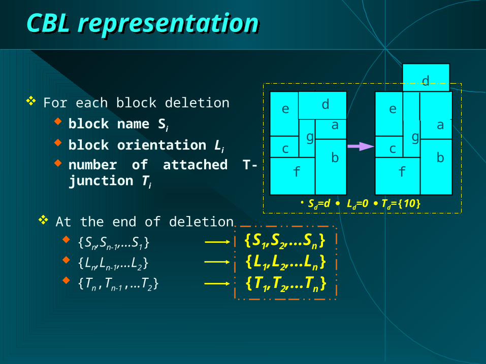
For each block deletion block name Si
block orientation Li
number of attached T-junction Ti
b
a
f
gc
e
• Sd=d Ld=0 Td={10}
b
a
f
gc
ed d
d
At the end of deletion {Sn,Sn-1,…S1} {Ln,Ln-1,…L2} {Tn,Tn-1,…T2}
{S1,S2,...Sn}{L1,L2,...Ln}{T1,T2,...Tn}
The Operation of CBThe Operation of CB
The deletion of CB
b
a
f
gc
e d
• Corner block ‘d’ is vertical and it is deleted.
• An attached T-junctions was pulled to the top.
b
a
f
gc
e d
d
The insertion of CB
b
a
f
gc
e
• Corner block ‘d’ is inserted from top.
• An attached T-junctions was covered.
b
a
f
gc
e d
OUTLINEOUTLINE
IntroductionIntroduction
Problem definitionProblem definition
Review of Corner Block ListReview of Corner Block List
Dead space partition while doing the packing
Computation of possible buffer insertion sites
Experimental Results
Conclusions
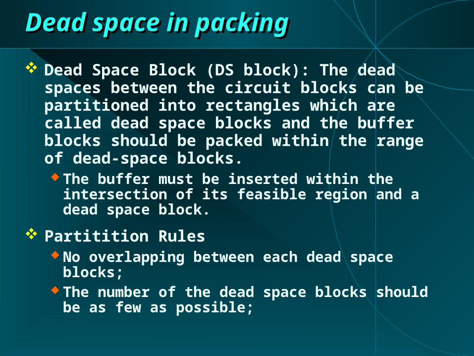
Dead space in packingDead space in packing
Dead Space Block (DS block): The dead spaces between the circuit blocks can be partitioned into rectangles which are called dead space blocks and the buffer blocks should be packed within the range of dead-space blocks. The buffer must be inserted within the intersection of
its feasible region and a dead space block.
Partitition Rules No overlapping between each dead space blocks; The number of the dead space blocks should be as few
as possible;
The dead space partitionThe dead space partition
Based on CBL, we propose the algorithm to obtain the dead space blocks in the floorplanning while doing the packing. The number of the dead space blocks(NDS) in CBL
packing should be less than n –1, where n is the number of the blocks.
The partition method will not generate overlapping between dead space blocks
Review of Corner Block ListReview of Corner Block List
Dead space partition while doing the packingDead space partition while doing the packing
Computation of possible buffer insertion sitesComputation of possible buffer insertion sites
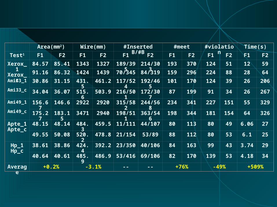
Experimental Results
Conclusions
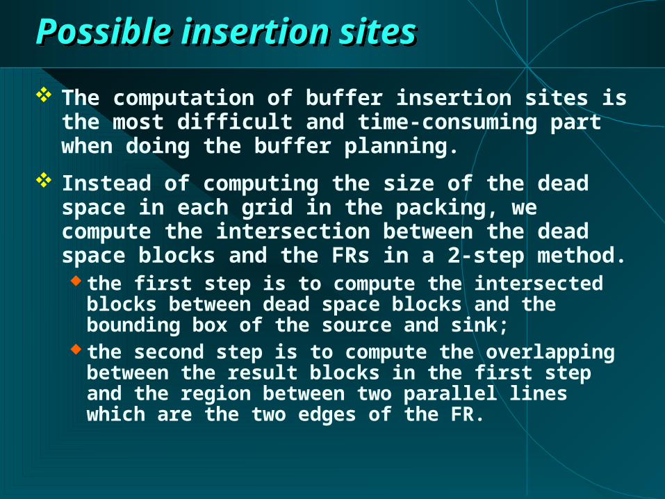
Possible insertion sitesPossible insertion sites
The computation of buffer insertion sites is the most difficult and time-consuming part when doing the buffer planning.
Instead of computing the size of the dead space in each grid in the packing, we compute the intersection between the dead space blocks and the FRs in a 2-step method. the first step is to compute the intersected blocks
between dead space blocks and the bounding box of the source and sink;
the second step is to compute the overlapping between the result blocks in the first step and the region between two parallel lines which are the two edges of the FR.
14 17 19 20
10 18
6 15
3 11
1 2 4 7
Possible buffer insertion sites
14 17 19 20
10 13 16 18
6 9 12 15
3 5 8 11
1 2 4 7
(a) slope is -1
20 19 17 14
18 16 13 10
15 12 9 6
11 8 5 3
7 4 2 1
(b) slope is +11
2 3
5
6
4
S
T
Possible buffer insertion sites are between grid 4 and grid 17
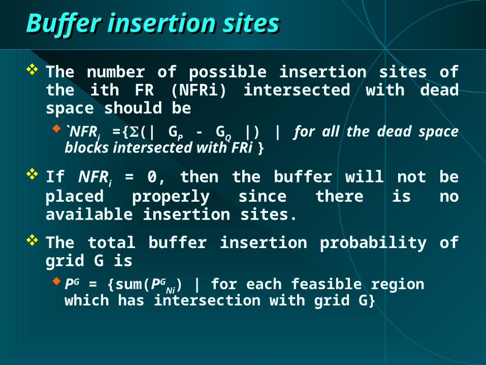
Buffer insertion sitesBuffer insertion sites
The number of possible insertion sites of the ith FR (NFRi) intersected with dead space should be `NFRi ={(| GP - GQ |) | for all the dead space blocks intersected
with FRi }
If NFRi = 0, then the buffer will not be placed properly since there is no available insertion sites.
The total buffer insertion probability of grid G is PG = {sum(PG
Ni) | for each feasible region which has intersection with grid G}
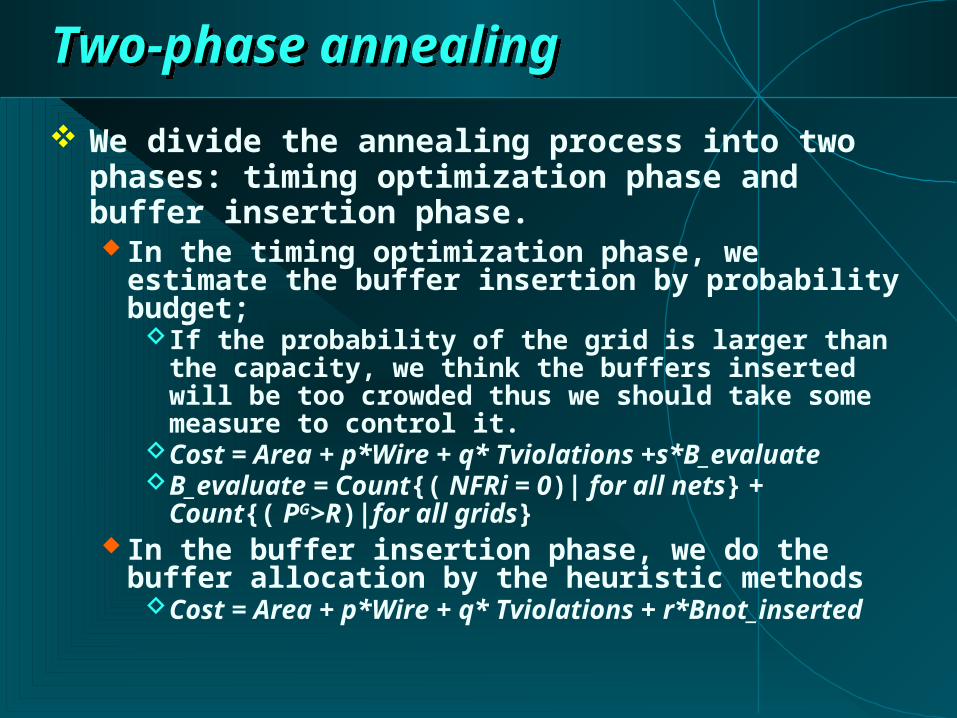
Two-phase annealingTwo-phase annealing
We divide the annealing process into two phases: timing optimization phase and buffer insertion phase. In the timing optimization phase, we estimate the buffer
insertion by probability budget;If the probability of the grid is larger than the capacity, we
think the buffers inserted will be too crowded thus we should take some measure to control it.
Cost = Area + p*Wire + q* Tviolations +s*B_evaluate B_evaluate = Count{( NFRi = 0)| for all nets} + Count{( PG>R)|for
all grids} In the buffer insertion phase, we do the buffer
allocation by the heuristic methodsCost = Area + p*Wire + q* Tviolations + r*Bnot_inserted
OUTLINEOUTLINE
IntroductionIntroduction
Problem definitionProblem definition
Review of Corner Block ListReview of Corner Block List
Dead space partition while doing the packingDead space partition while doing the packing
Computation of possible buffer insertion sitesComputation of possible buffer insertion sites
The buffer allocation is handled as an integral part in the floorplanning process.
Not necessarily to scan the whole packing to find the dead spaces, we can partition the dead space into blocks while doing the packing.
Instead of computing the size of the dead space in each grid, we compute the intersection between the dead space blocks and the FRs in a 2-step method.
The experiments prove the effectiveness of our approach.


![Floorplanning - National Taiwan Universitycc.ee.ntu.edu.tw/~ywchang/Courses/PD_Source/EDA_floorplanning.pdf · Sherwani 1999]. Basically, simulated annealing-based floorplanning relies](https://static.documents.pub/doc/80x56/5a79a4137f8b9a28678c4078/floorplanning-national-taiwan-ywchangcoursespdsourceedafloorplanningpdfsherwani.jpg)


