Andrew Kahng – October 2001 913.001 Layout Techniques for Cost- Driven Control of Lithography-Induced Variability Dennis Sylvester / Andrew B. Kahng U. Michigan EECS Dept. / UC San Diego ECE Dept.
Transcript
Andrew Kahng – October 2001
913.001 Layout Techniques for Cost-Driven Control of Lithography-Induced Variability
Dennis Sylvester / Andrew B. KahngU. Michigan EECS Dept. / UC San Diego ECE Dept.
Andrew Kahng – October 2001
Project OverviewObjective: Develop cost models, design rules, layout methods, and tools to: (1) minimize costs associated with resolution enhancement techniques (RETs), and (2) limit lithography-induced variability• Faculty
– Dennis Sylvester, University of Michigan EECS Dept.– Andrew B. Kahng, University of California, San Diego ECE Dept.
diagonal features)– Cost-reducing variants (IDEAL, GRATEFUL) more constraining
• Process window and yield enhancement: ditto– Forbidden width-spacing combinations (defocus window
sensitivities)– Complex “local DRCs”
• OPC subresolution assist features: ditto– Notch rules, critical-feature rules on local metal
• Other– Dummy fill changes RCX results, creates inter-layer
dependencies, increases data volume– halation rules (width- and length-dependent spacing)
Andrew Kahng – October 2001
Example: Off-Axis Illumination
• Different variants of off-axis illumination act to:– Amplify dense lines while attentuating larger pitches– Print only axis-parallel lines, not 45º lines
F. Schellenberg, Mentor
Andrew Kahng – October 2001
RET-Related Needs in 2001 ITRS• Function- and cost-aware OPC, PSM, dummy fill• Real goal = predictable circuit performance and function• Tools must understand functional intent
– Make only corrections that gain $$$, reduce performance variation– Make only corrections that can be manufactured and verified – Fail only mask errors that affect function– Understand (data volume, verification) costs of breaking hierarchy
• Fix broken flows– Making same OPC corrections 3x (library, router, PV tool)– Layout signoff w/o comprehending later RET insertion (e.g., fill)
Andrew Kahng – October 2001
Key Question
Which should be developed: (A) circuit design techniques that can deal with variability, or (B) process techniques that reduce variability?
• At < 65nm, variation-tolerant circuit techniques may be a more cost-effective way to combat rising process uncertainties
• Should seek better bang for the buck in applying RETs– Function-, cost-driven corrections– Synergies among various correction techniques (e.g., fill helps OPC)
Andrew Kahng – October 2001
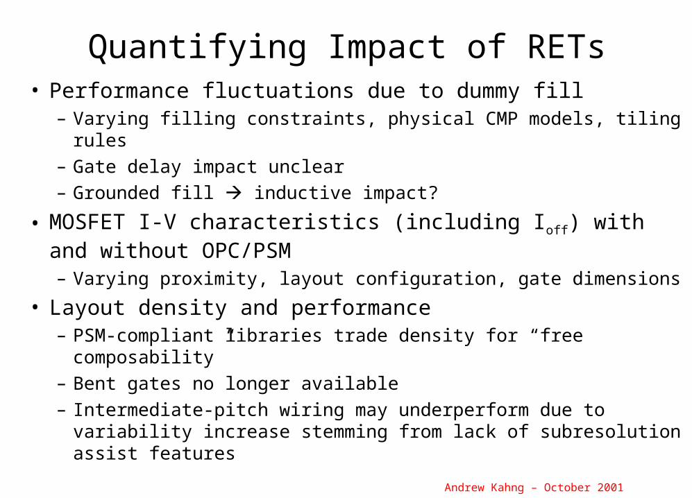
Quantifying Impact of RETs• Performance fluctuations due to dummy fill
• MOSFET I-V characteristics (including Ioff) with and without OPC/PSM– Varying proximity, layout configuration, gate dimensions
• Layout density and performance– PSM-compliant libraries trade density for “free composability”– Bent gates no longer available– Intermediate-pitch wiring may underperform due to variability
increase stemming from lack of subresolution assist features
Andrew Kahng – October 2001
Investigating the Variability/Cost Relationship
Initial driving question: How does the maximum value design compare to the maximum performance design?
• Maximum value is driven by parametric distributions as well as value distributions (e.g., bin sorting)
• What are the design implications for a value maximized design?– E.g., rely more heavily on spatial correlations or strive for more random
behavior (averaging effects) ???• To measure $/wafer, we need (1) detailed models of process
variability, and (2) models of how chip parameters (frequency, testability, etc.) affect value
Andrew Kahng – October 2001
Investigating the Variability/Cost Relationship (1)
• (A) Build a taxonomy of variability sources– Intrinsic vs. dynamic (Vdd,temp)– Random vs. systematic– Intra-die, Intra-reticle, Intra-wafer, etc.– Including correlations (local, global)
• (B) Incorporate a smart Monte Carlo approach– Based on performance sensitivity to sources of uncertainty
• (C) Build generic critical path models– Delay-constrained vs. power-constrained– + Ring-oscillator, clock tree, etc. models
Andrew Kahng – October 2001
“Mapping Design to Value”: (1)
Across-Wafer Frequency Variation
Andrew Kahng – October 2001
“Mapping Design to Value”: (1)
Across-Wafer Frequency Variation
Andrew Kahng – October 2001
AMD Processors
0
50
100
150
200
250
300
350
400
450
0 200 400 600 800 1000 1200 1400 1600
Clock Speed (MHz)
Pri
ce
($
)
Athlon MP
Athlon 4 Mobile
Athlon Desktop
Duron
Duron Mobile
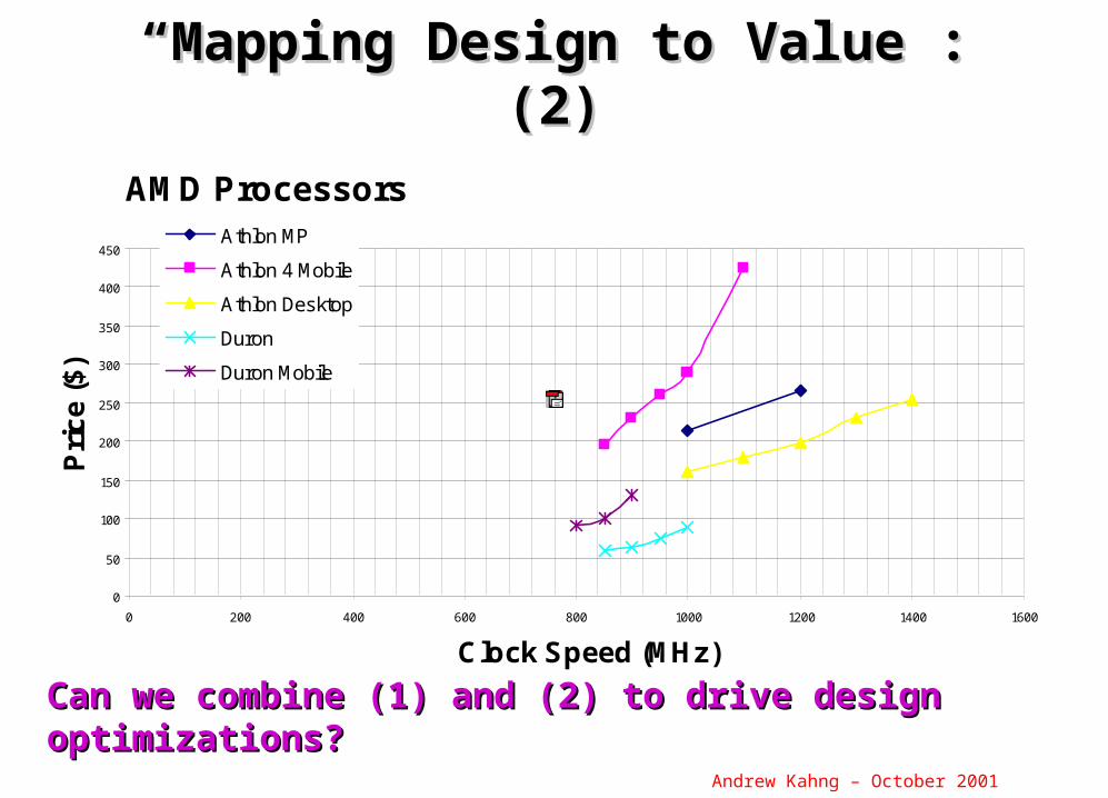
““Mapping Design to Value”: (2)Mapping Design to Value”: (2)
Can we combine (1) and (2) to drive design optimizations?Can we combine (1) and (2) to drive design optimizations?
Andrew Kahng – October 2001
““Mapping Design to Value”: (2)Mapping Design to Value”: (2)
Can we combine (1) and (2) to drive design optimizations?Can we combine (1) and (2) to drive design optimizations?
Andrew Kahng – October 2001
Research Timeline
• Year 1: Assess cost vs. variability tradeoffs, develop cost models for RETs
• Year 2: Develop layout methods and tools for cost-driven insertion of RETs while meeting performance goals
• Year 3: Model calibration/verification using test structures, circuit layout approaches to account for RET-based constraints
Andrew Kahng – October 2001
SPARE SLIDES
Andrew Kahng – October 2001
RET Resource Requirements
1
10
100
1000
1997 1998 1999 2000 2001
Year
Res
ou
rce
s Data Size/Layer
# RET Layers
# CPU's
Hours
Gate Mask Production (Days)
Grobman, Motorola
Andrew Kahng – October 2001
RET RoadmapRET Roadmap
Rule-based OPC
Model-based OPC
Scattering Bars
AA-PSM
Weak PSM
Rule-based Tiling
Optimization-driven MB Tiling
0.25 um 0.18 um 0.13 um 0.10 um 0.07 um
248 nm
248/193 nm
193 nm
Number Of Affected Layers Increases / Generation
Litho
CMP
W. Grobman, Motorola – DAC-2001
Andrew Kahng – October 2001
Mask Data and the $1M Mask NREMask Data and the $1M Mask NRE• Too many data formats
– Most tools have unique data format– Raster to variable shaped-beam conversion is inefficient– Real-time manufacturing tool switch, multiple qualified tools
duplicate fractures to avoid delays if tool switch required• Data volume
– OPC increases figure count acceleration– MEBES format is flat– ALTA machines (mask writers) slow down with > 1GB data– Data volume strains distributed manufacturing resources
• Refracturing mask data– Before: mask industry never touched mask data (risky, no good
reason)– Today: 90% of mask data files manipulated or refractured: