Sp12 CMPEN 411 L24 S.1
CMPEN 411VLSI Digital Circuits
Spring 2012
Lecture 24: Peripheral Memory Circuits
[Adapted from Rabaey’s Digital Integrated Circuits, Second Edition, ©2003 J. Rabaey, A. Chandrakasan, B. Nikolic]
Sp12 CMPEN 411 L24 S.2
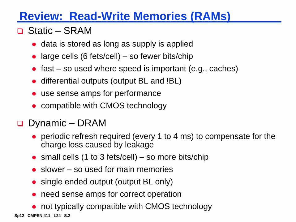
Review: Read-Write Memories (RAMs)
Static – SRAM
data is stored as long as supply is applied
large cells (6 fets/cell) – so fewer bits/chip
fast – so used where speed is important (e.g., caches)
differential outputs (output BL and !BL)
use sense amps for performance
compatible with CMOS technology
Dynamic – DRAM
periodic refresh required (every 1 to 4 ms) to compensate for the charge loss caused by leakage
small cells (1 to 3 fets/cell) – so more bits/chip
slower – so used for main memories
single ended output (output BL only)
need sense amps for correct operation
not typically compatible with CMOS technology
Sp12 CMPEN 411 L24 S.6
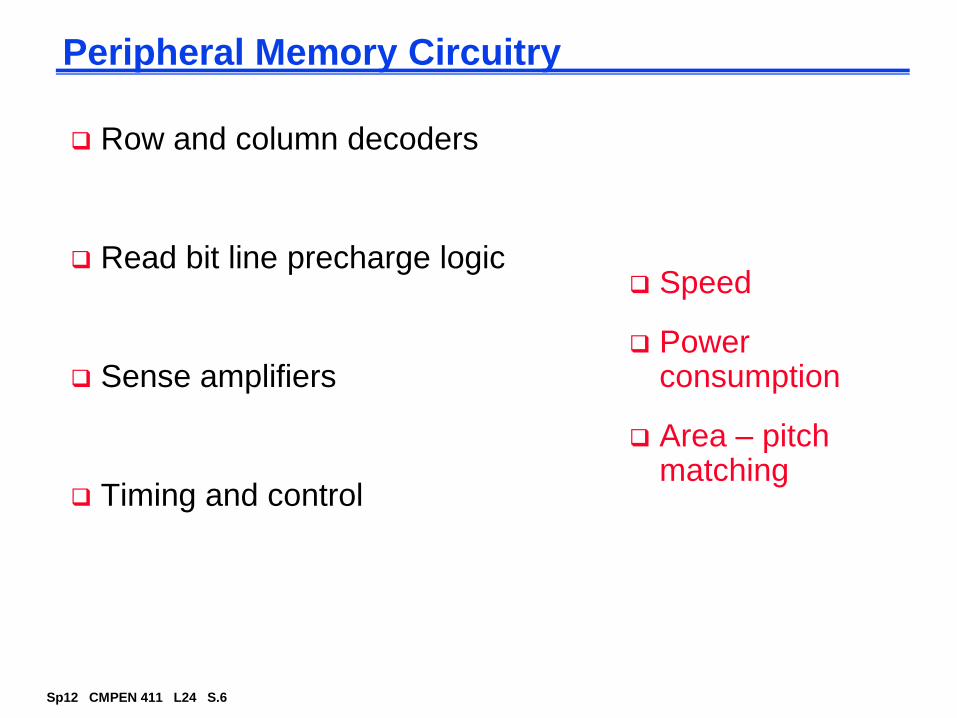
Peripheral Memory Circuitry
Row and column decoders
Read bit line precharge logic
Sense amplifiers
Timing and control
Speed
Power consumption
Area – pitch matching
Sp12 CMPEN 411 L24 S.7
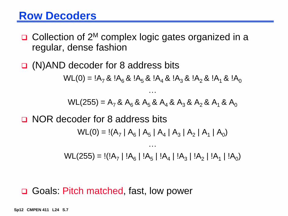
Row Decoders
Collection of 2M complex logic gates organized in a regular, dense fashion
(N)AND decoder for 8 address bits
WL(0) = !A7 & !A6 & !A5 & !A4 & !A3 & !A2 & !A1 & !A0
…
WL(255) = A7 & A6 & A5 & A4 & A3 & A2 & A1 & A0
NOR decoder for 8 address bits
WL(0) = !(A7 | A6 | A5 | A4 | A3 | A2 | A1 | A0)
…
WL(255) = !(!A7 | !A6 | !A5 | !A4 | !A3 | !A2 | !A1 | !A0)
Goals: Pitch matched, fast, low power
Sp12 CMPEN 411 L24 S.8
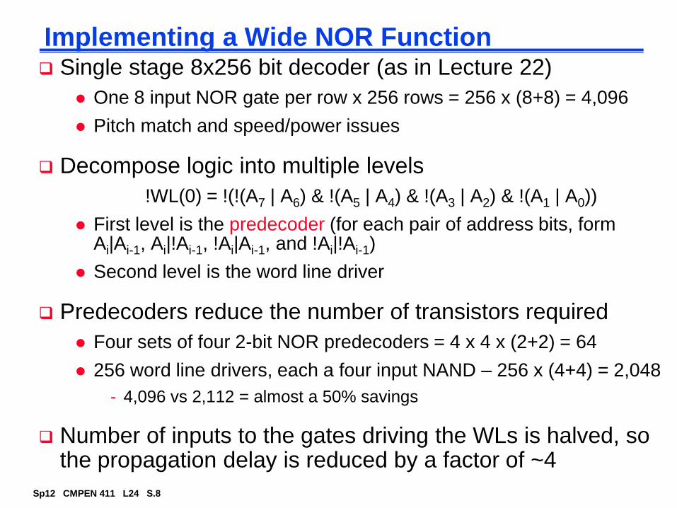
Implementing a Wide NOR Function Single stage 8x256 bit decoder (as in Lecture 22)
One 8 input NOR gate per row x 256 rows = 256 x (8+8) = 4,096
Pitch match and speed/power issues
Decompose logic into multiple levels
!WL(0) = !(!(A7 | A6) & !(A5 | A4) & !(A3 | A2) & !(A1 | A0))
First level is the predecoder (for each pair of address bits, form Ai|Ai-1, Ai|!Ai-1, !Ai|Ai-1, and !Ai|!Ai-1)
Second level is the word line driver
Predecoders reduce the number of transistors required
Four sets of four 2-bit NOR predecoders = 4 x 4 x (2+2) = 64
256 word line drivers, each a four input NAND – 256 x (4+4) = 2,048
- 4,096 vs 2,112 = almost a 50% savings
Number of inputs to the gates driving the WLs is halved, so the propagation delay is reduced by a factor of ~4
Sp12 CMPEN 411 L24 S.9
Hierarchical Decoders
• • •
• • •
A2A2
A 2A3
WL 0
A2A3A2A 3A2A3
A3 A3A 0A0
A0A 1A 0A1A0A1A0A1
A 1 A1
WL 1
Multi-stage implementation improves performance
NAND decoder using
2-input pre-decoders
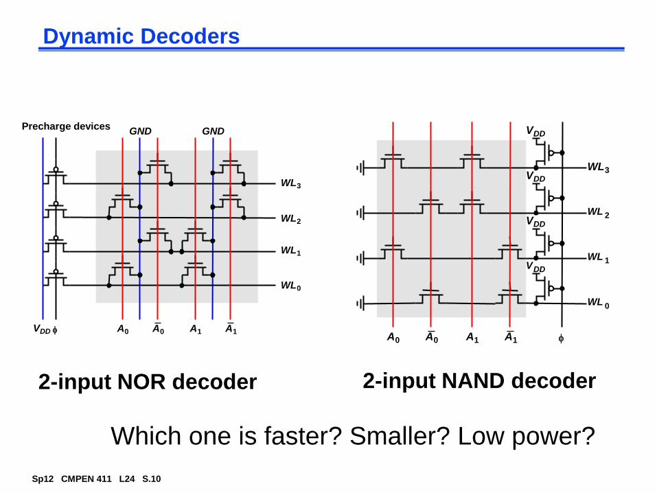
Sp12 CMPEN 411 L24 S.10
Dynamic Decoders
Precharge devices
VDD f
GND
WL3
WL2
WL1
WL0
A0A0
GND
A1A1f
WL3
A0A0 A1A1
WL 2
WL 1
WL 0
VDD
VDD
VDD
VDD
2-input NOR decoder 2-input NAND decoder
Which one is faster? Smaller? Low power?
Sp12 CMPEN 411 L24 S.11
Pass Transistor Based Column Decoder
BL3 BL2 BL1 BL0
data_out
2 input
NO
R d
ecoder
A1
A0
S3
S2
S1
S0
Read: connect BLs to the Sense Amps (SA) Writes: drive one of the BLs low to write a 0 into the cell
Fast since there is only one transistor in the signal path. However, there is a large transistor count ( (K+1)2K + 2 x 2K)
For K = 2 3 x 22 (decoder) + 2 x 22 (PTs) = 12 + 8 = 20
!BL3 !BL2 !BL1 !BL0
!data_out
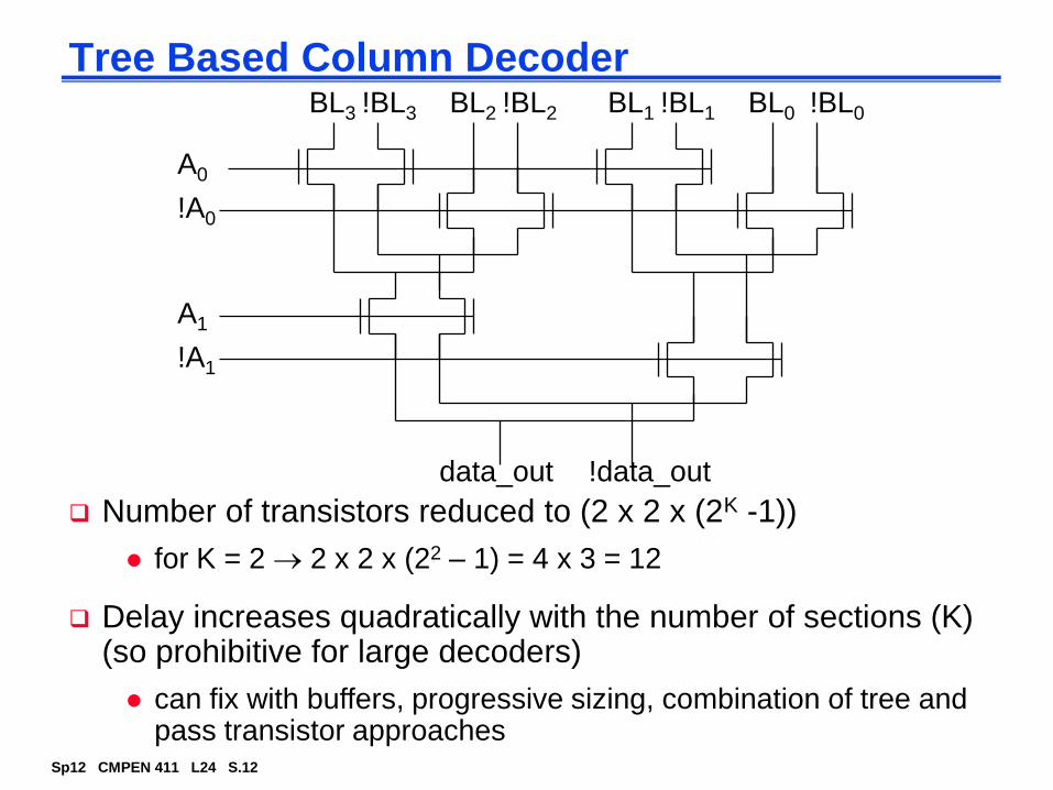
Sp12 CMPEN 411 L24 S.12
Tree Based Column DecoderBL3 BL2 BL1 BL0
A0
!A0
A1
!A1
data_out
Number of transistors reduced to (2 x 2 x (2K -1))
for K = 2 2 x 2 x (22 – 1) = 4 x 3 = 12
Delay increases quadratically with the number of sections (K) (so prohibitive for large decoders)
can fix with buffers, progressive sizing, combination of tree and pass transistor approaches
!BL3 !BL2 !BL1 !BL0
!data_out
Sp12 CMPEN 411 L24 S.13
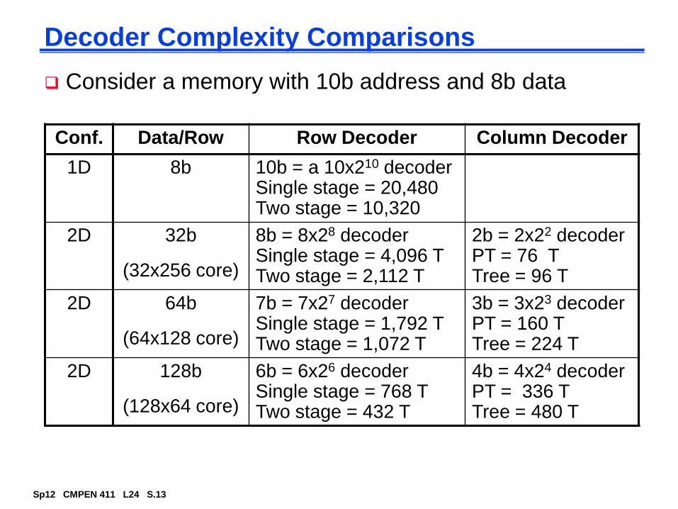
Decoder Complexity Comparisons
Consider a memory with 10b address and 8b data
Conf. Data/Row Row Decoder Column Decoder
1D 8b 10b = a 10x210 decoder Single stage = 20,480 Two stage = 10,320
2D 32b
(32x256 core)
8b = 8x28 decoder Single stage = 4,096 T Two stage = 2,112 T
2b = 2x22 decoder PT = 76 T Tree = 96 T
2D 64b
(64x128 core)
7b = 7x27 decoder Single stage = 1,792 T Two stage = 1,072 T
3b = 3x23 decoder PT = 160 T Tree = 224 T
2D 128b
(128x64 core)
6b = 6x26 decoder Single stage = 768 T Two stage = 432 T
4b = 4x24 decoder PT = 336 T Tree = 480 T
Sp12 CMPEN 411 L24 S.14
Bit Line Precharge Logic
equalization transistor - speeds up
equalization of the two bit lines by
allowing the capacitance and pull-up
device of the nondischarged bit line to
assist in precharging the discharged
line
!PC
!BLBL
First step of a Read cycle is to precharge (PC) the bit lines to VDD
every differential signal in the memory must be equalized to the same voltage level before Read
Turn off PC and enable the WL
the grounded PMOS load limits the bit line swing (speeding up the next precharge cycle)
Sp12 CMPEN 411 L24 S.15
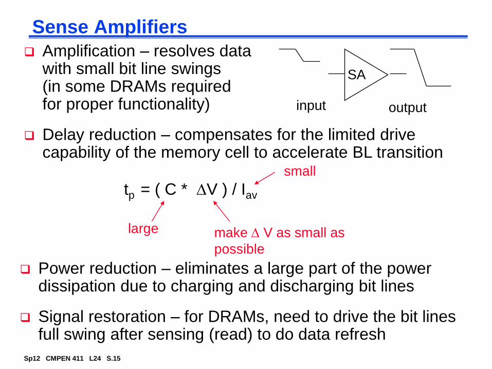
Sense Amplifiers
Amplification – resolves data with small bit line swings (in some DRAMs required for proper functionality)
Delay reduction – compensates for the limited drive capability of the memory cell to accelerate BL transition
SA
input output
tp = ( C * V ) / Iav
large
small
make V as small as
possible
Power reduction – eliminates a large part of the power dissipation due to charging and discharging bit lines
Signal restoration – for DRAMs, need to drive the bit lines full swing after sensing (read) to do data refresh
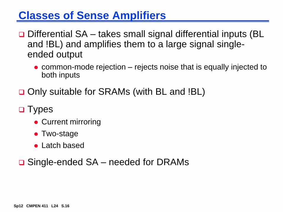
Sp12 CMPEN 411 L24 S.16
Classes of Sense Amplifiers
Differential SA – takes small signal differential inputs (BL and !BL) and amplifies them to a large signal single-ended output
common-mode rejection – rejects noise that is equally injected to both inputs
Only suitable for SRAMs (with BL and !BL)
Types
Current mirroring
Two-stage
Latch based
Single-ended SA – needed for DRAMs
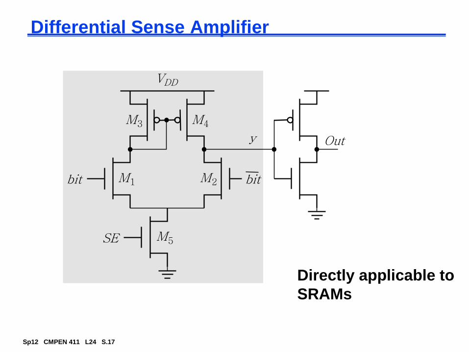
Sp12 CMPEN 411 L24 S.17
Differential Sense Amplifier
Directly applicable to
SRAMs
M4
M1
M5
M3
M2
VDD
bitbit
SE
Outy
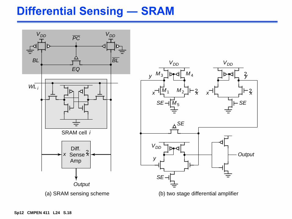
Sp12 CMPEN 411 L24 S.18
Differential Sensing ― SRAM
VDD
VDD
VDD
VDD
BL
EQ
Diff.SenseAmp
(a) SRAM sensing scheme (b) two stage differential amplifier
SRAM cell i
WL i
2xx
VDD
Output
BL
PC
M3
M1
M5
M2
M4
x
SE
SE
SE
Output
SE
x2x 2x
y
y
2y
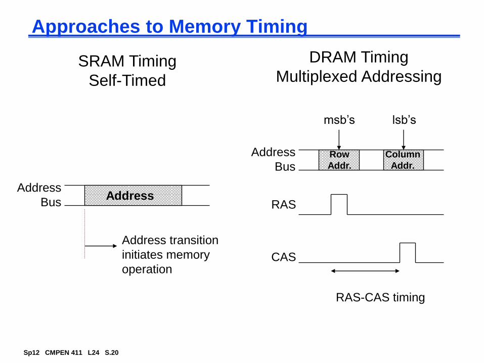
Sp12 CMPEN 411 L24 S.20
Approaches to Memory Timing
DRAM Timing
Multiplexed Addressing
RAS
CAS
RAS-CAS timing
Address
Bus
msb’s lsb’s
Row
Addr.
Column
Addr.
Address
Bus
SRAM Timing
Self-Timed
Address
Address transition
initiates memory
operation
Sp12 CMPEN 411 L24 S.21
Reliability and Yield
Memories operate under low signal-to-noise conditions
word line to bit line coupling can vary substantially over the memory array
- folded bit line architecture (routing BL and !BL next to each other ensures a closer match between parasitics and bit line capacitances)
interwire bit line to bit line coupling
- transposed (or twisted) bit line architecture (turn the noise into a common-mode signal for the SA)
leakage (in DRAMs) requiring refresh operation
suffer from low yield due to high density and structural defects
increase yield by using error correction (e.g., parity bits) and redundancy
and are susceptible to soft errors due to alpha particles and cosmic rays
Sp12 CMPEN 411 L24 S.22
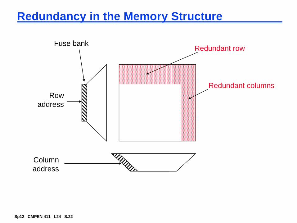
Redundancy in the Memory Structure
Row
address
Column
address
Redundant row
Redundant columns
Fuse bank
Sp12 CMPEN 411 L24 S.23
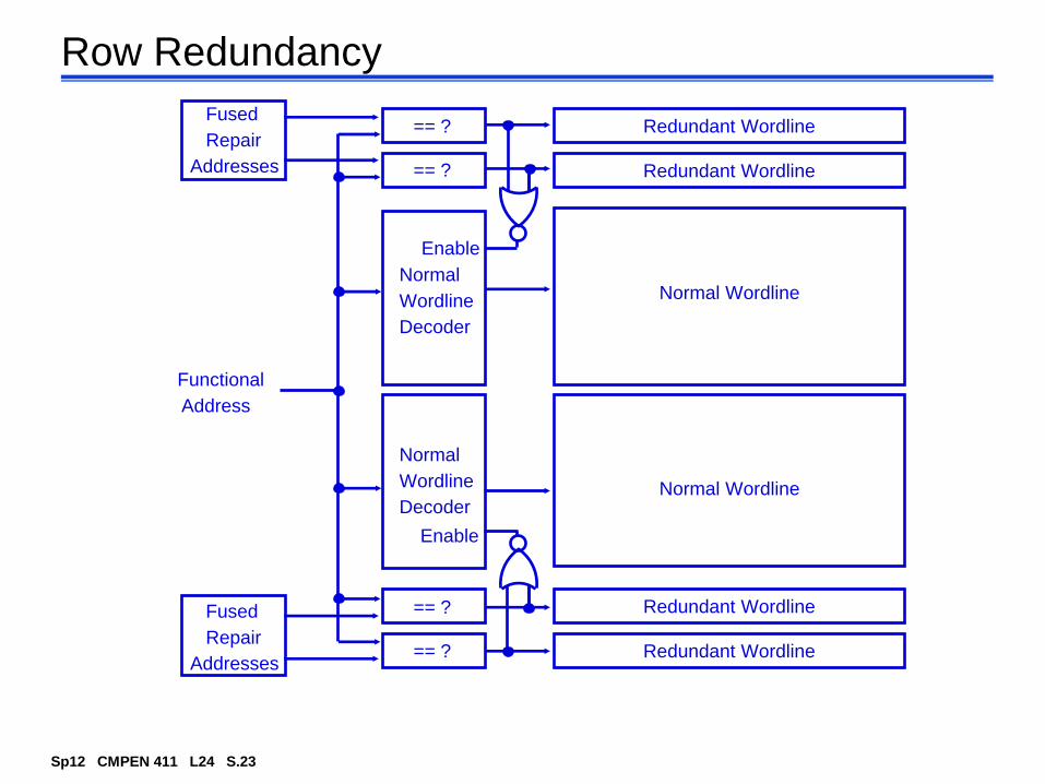
Page 4
== ?
== ?
Redundant Wordline
Redundant Wordline
Fused
Repair
Addresses
Enable
Normal
Wordline
Decoder
Normal Wordline
Functional
Address
== ?
== ?
Redundant Wordline
Redundant WordlineFused
Repair
Addresses
Enable
Normal
Wordline
DecoderNormal Wordline
Row Redundancy
Sp12 CMPEN 411 L24 S.24
Page 5
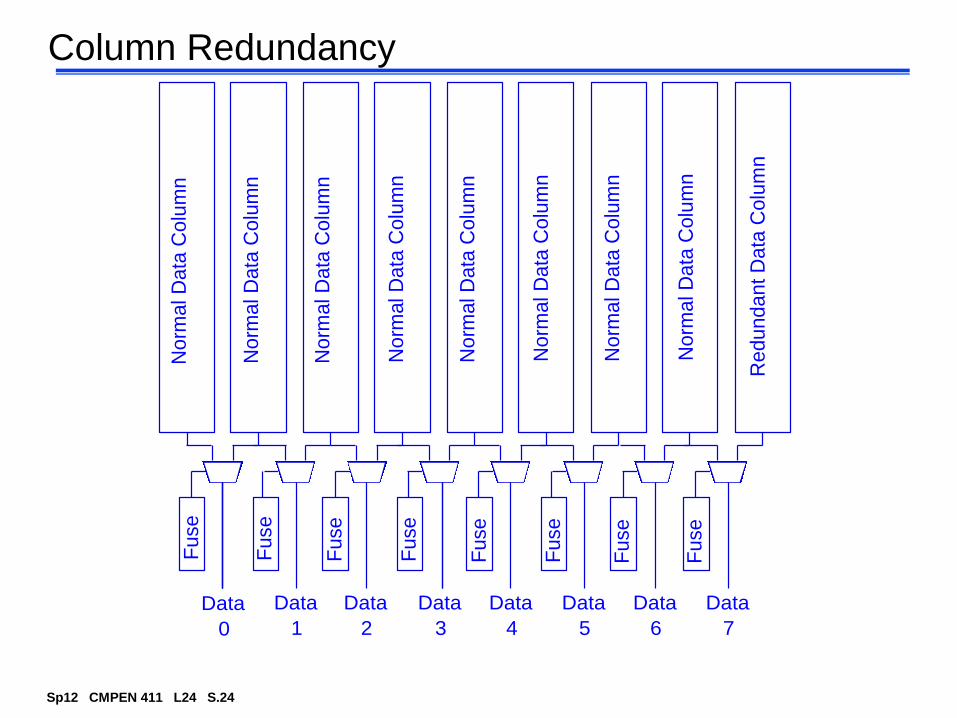
Column Redundancy
Re
du
nd
an
t D
ata
Colu
mn
No
rma
l D
ata
Co
lum
n
No
rma
l D
ata
Co
lum
n
No
rma
l D
ata
Co
lum
n
No
rma
l D
ata
Co
lum
n
No
rma
l D
ata
Co
lum
n
No
rma
l D
ata
Co
lum
n
No
rma
l D
ata
Co
lum
n
No
rma
l D
ata
Co
lum
nF
use
Fu
se
Fu
se
Fu
se
Fu
se
Fu
se
Fu
se
Fu
se
Data
0
Data
1
Data
2
Data
3
Data
4
Data
5
Data
7
Data
6
Sp12 CMPEN 411 L24 S.25
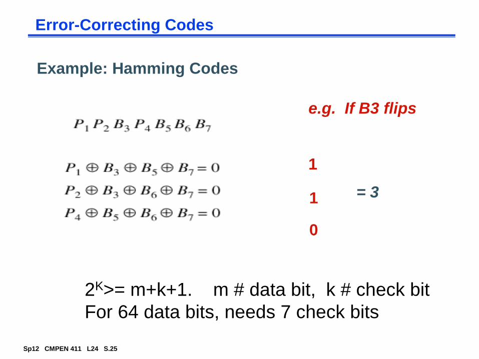
Error-Correcting Codes
Example: Hamming Codes
e.g. If B3 flips
1
1
0
= 3
2K>= m+k+1. m # data bit, k # check bit
For 64 data bits, needs 7 check bits
Sp12 CMPEN 411 L24 S.26
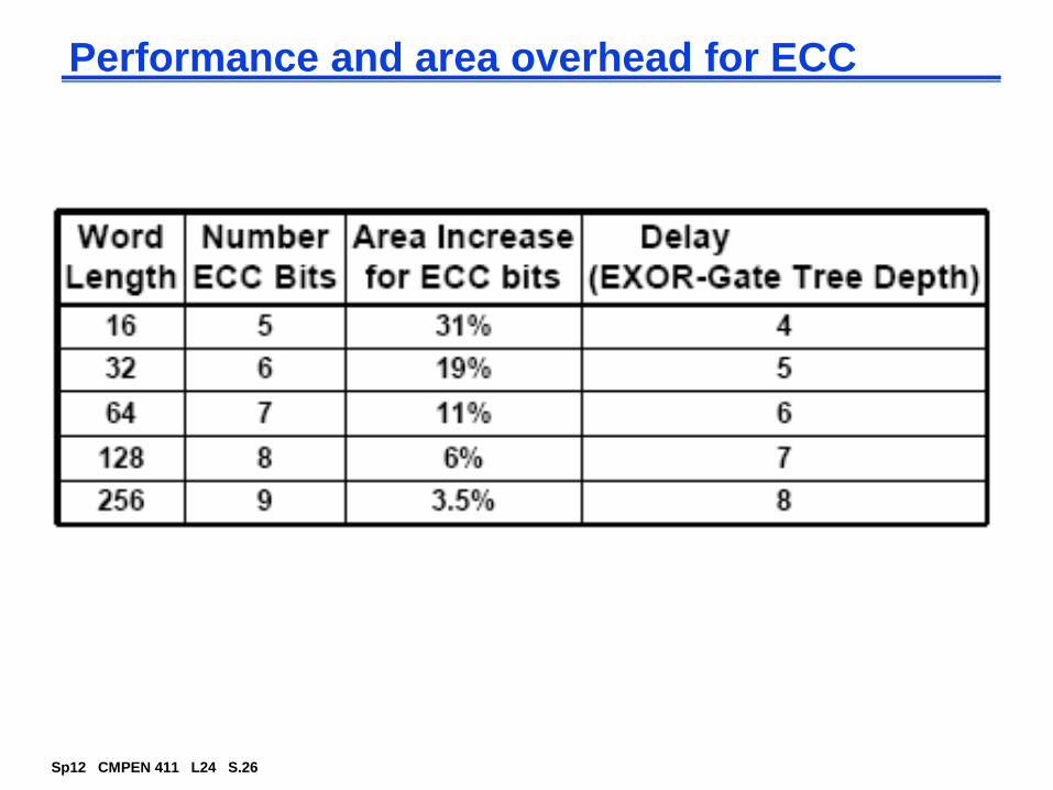
Performance and area overhead for ECC
Sp12 CMPEN 411 L24 S.27
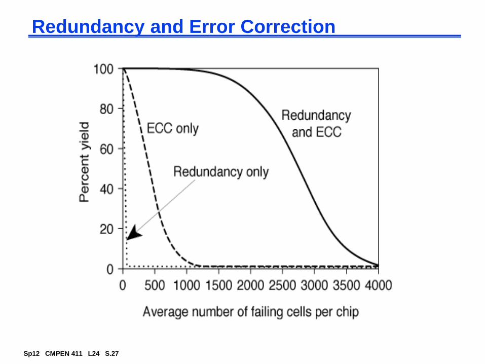
Redundancy and Error Correction
Sp12 CMPEN 411 L24 S.28
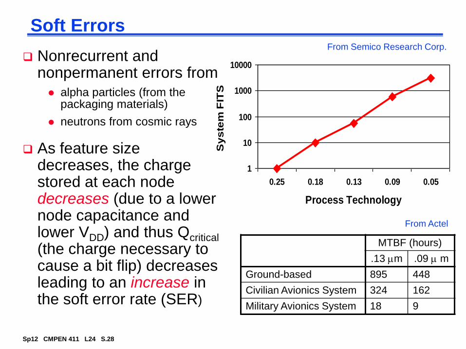
Soft Errors
Nonrecurrent and nonpermanent errors from
alpha particles (from the packaging materials)
neutrons from cosmic rays
As feature size decreases, the charge stored at each node decreases (due to a lower node capacitance and lower VDD) and thus Qcritical
(the charge necessary to cause a bit flip) decreases leading to an increase in the soft error rate (SER)
1
10
100
1000
10000
0.25 0.18 0.13 0.09 0.05
Process Technology
Sy
ste
m F
ITS
From Semico Research Corp.
MTBF (hours)
.13 m .09 m
Ground-based 895 448
Civilian Avionics System 324 162
Military Avionics System 18 9
From Actel
Sp12 CMPEN 411 L24 S.29
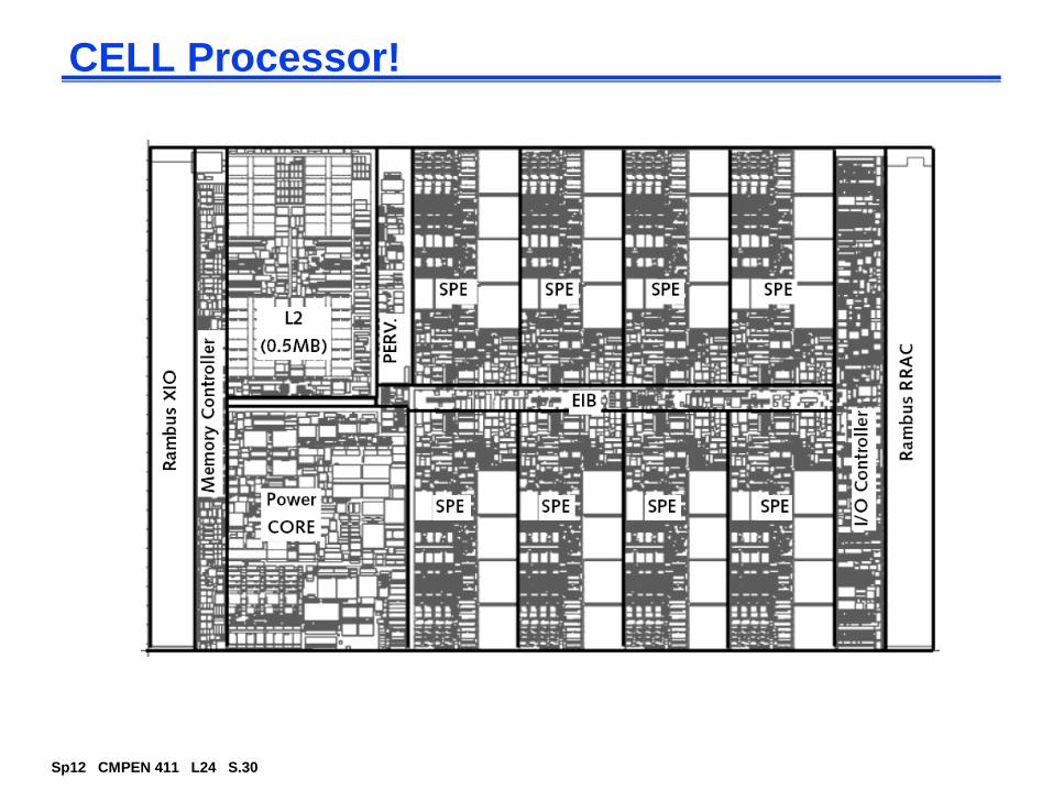
CELL Processor!
See class website for web links
Sp12 CMPEN 411 L24 S.30
CELL Processor!
Sp12 CMPEN 411 L24 S.31
CELL Processor!
Sp12 CMPEN 411 L24 S.32
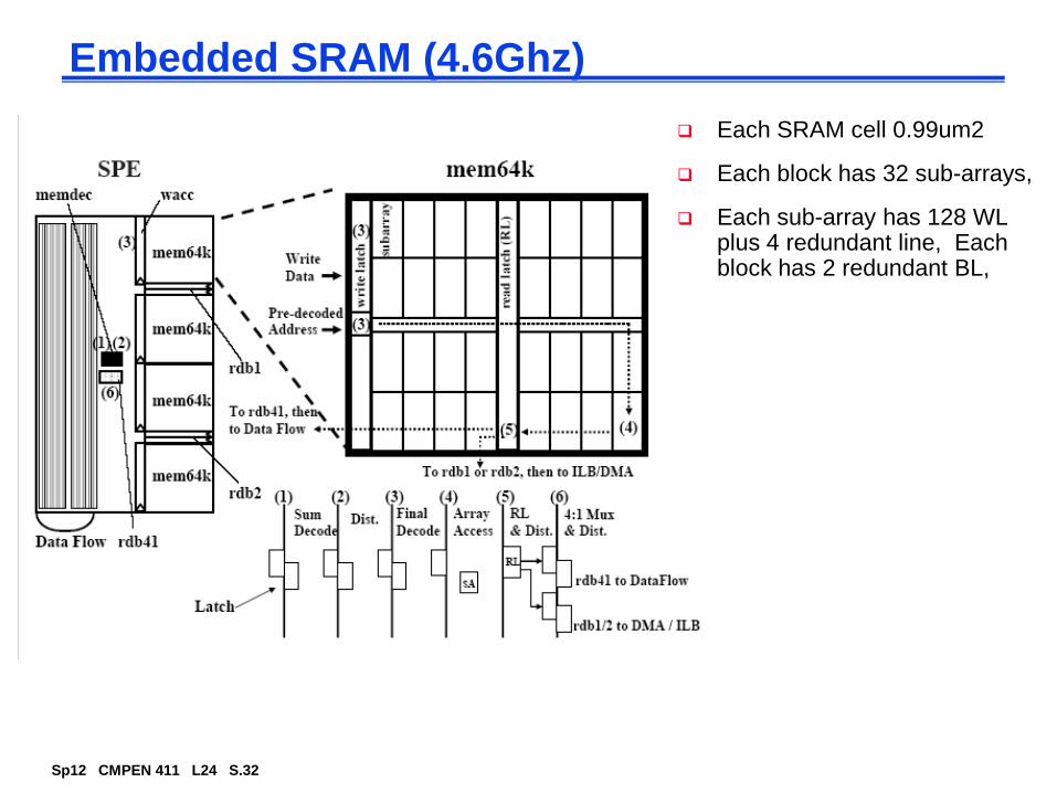
Embedded SRAM (4.6Ghz)
Each SRAM cell 0.99um2
Each block has 32 sub-arrays,
Each sub-array has 128 WL plus 4 redundant line, Each block has 2 redundant BL,
Sp12 CMPEN 411 L24 S.33
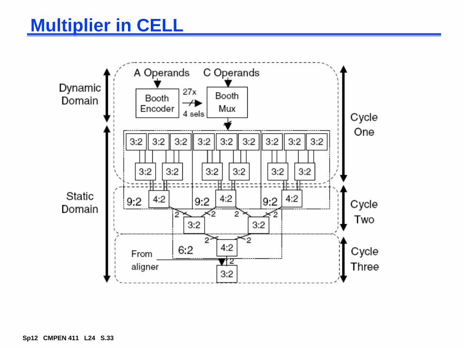
Multiplier in CELL
Sp12 CMPEN 411 L24 S.34
Next Lecture and Reminders
Next lecture
Power consumption in datapaths and memories
- Reading assignment – Rabaey, et al, 11.7; 12.5