Halogen and Antimony Free. “Green” Device (Note 3)
Pin Assignments
(Top View) (Top View)
SOT23 (Package Code: N) SOT23 (Package Code: N1)
(Top View) (Top View)
SOT89 (Option 1) SOT89 (Option 2)
(Top View)
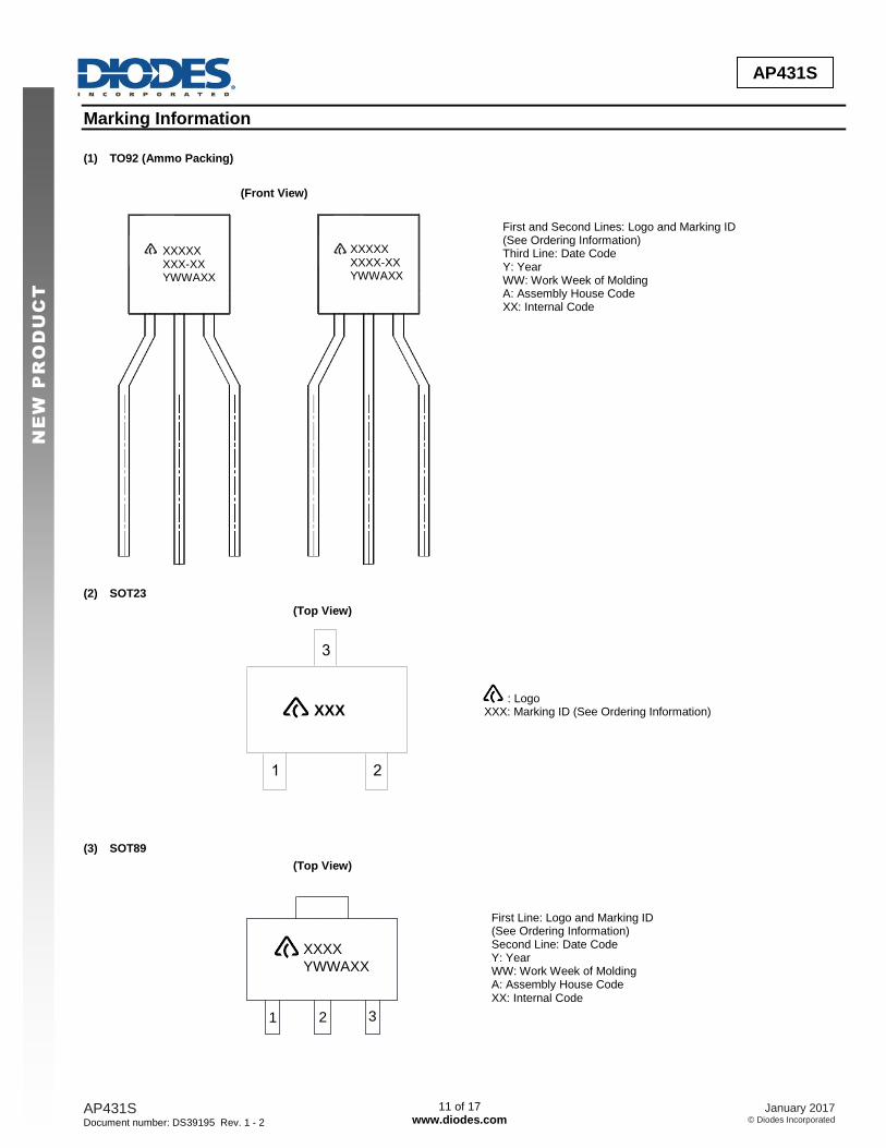
TO92 (Ammo Packing)
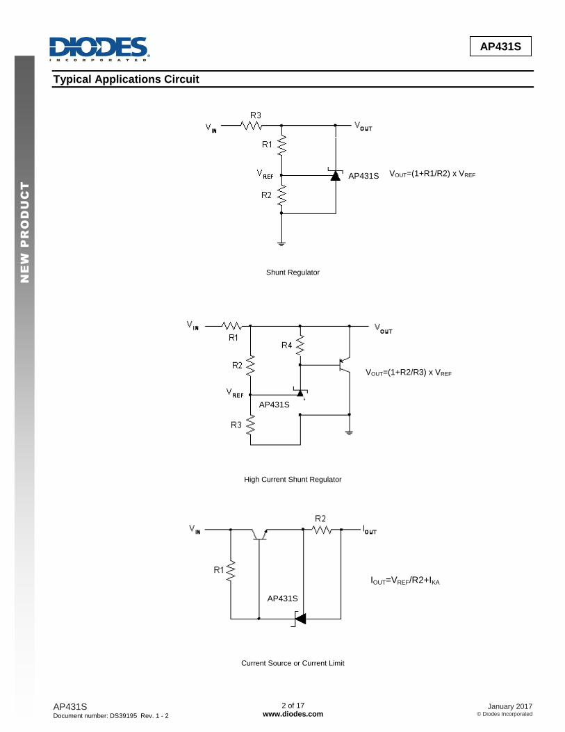
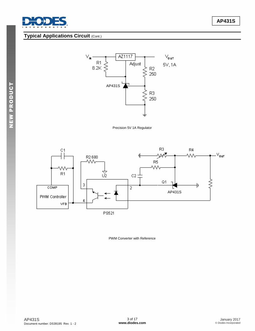
Applications
Charger
Voltage Adapter
Switching Power Supply
Graphic Card
Precision Voltage Reference
Notes: 1. No purposely added lead. Fully EU Directive 2002/95/EC (RoHS) & 2011/65/EU (RoHS 2) compliant.
2. See http://www.diodes.com/quality/lead_free.html for more information about Diodes Incorporated’s definitions of Halogen- and Antimony-free, "Green"
and Lead-free.
3. Halogen- and Antimony-free "Green” products are defined as those which contain <900ppm bromine, <900ppm chlorine (<1500ppm total Br + Cl) and
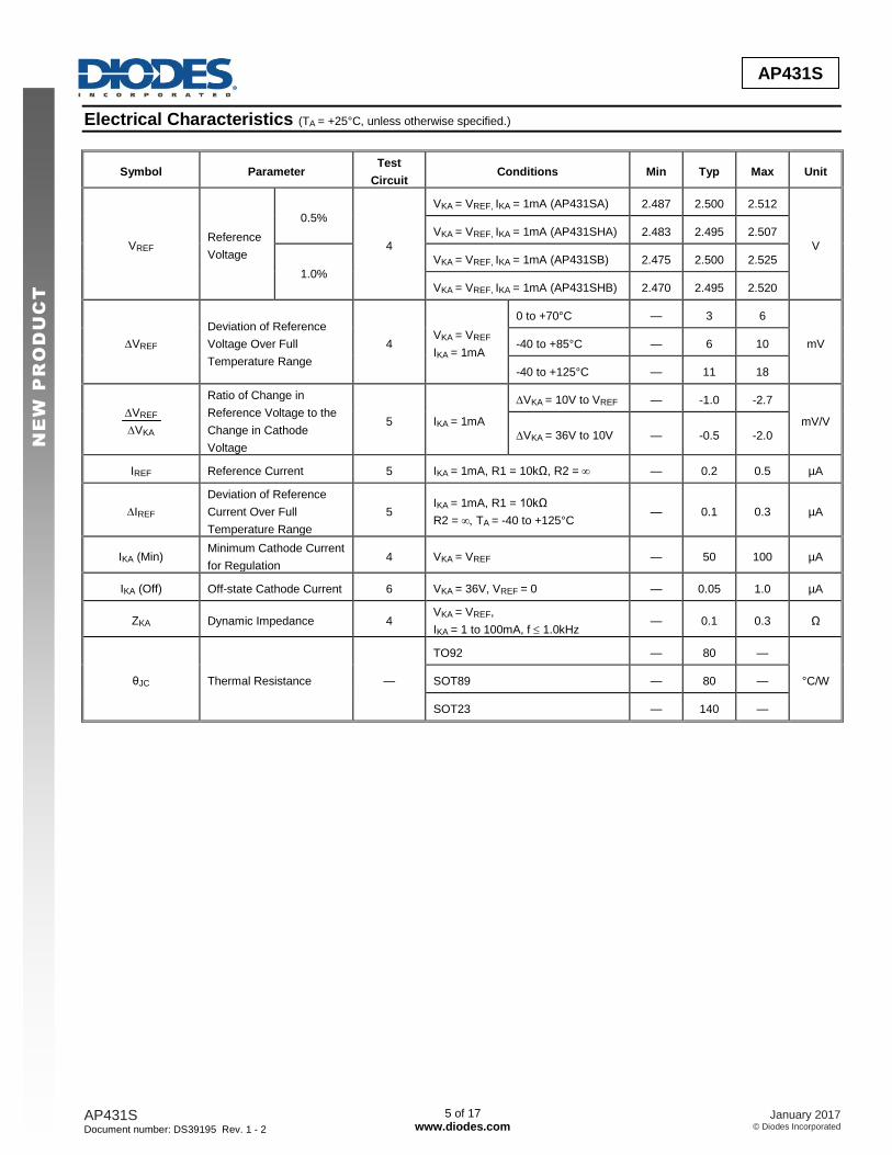
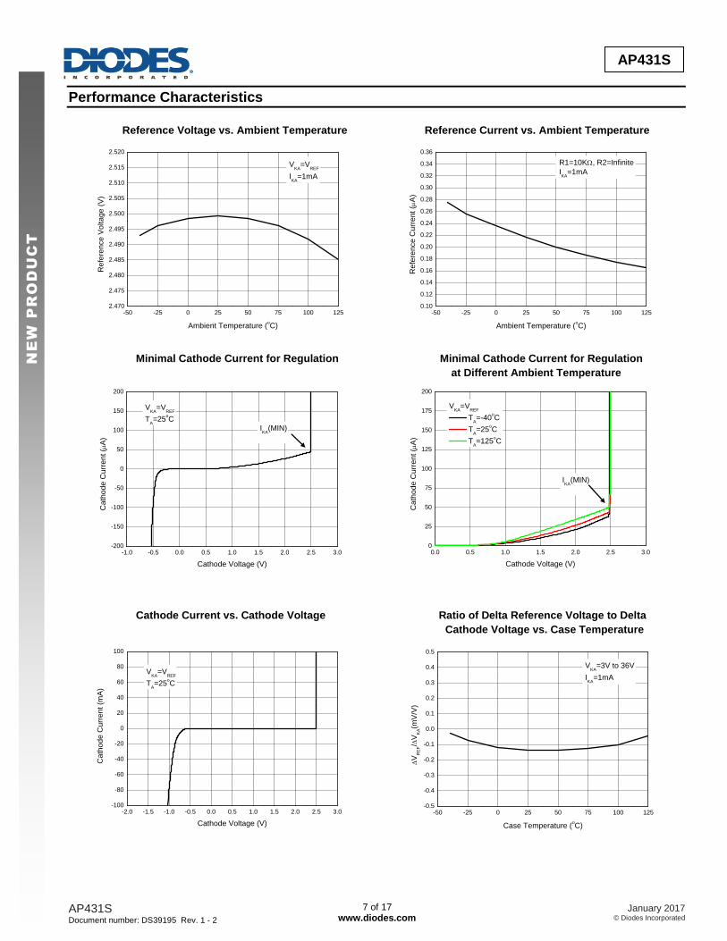
IKA Cathode Current Range (Continuous) -100 to 150 mA
IREF Reference Input Current Range 10 mA
PD Power Dissipation
TO92 750
mW SOT89 750
SOT23 350
TJ Junction Temperature +150 °C
TSTG Storage Temperature Range -65 to +150 °C
ESD ESD (Human Body Model) 5,500 V
ESD ESD (Machine Model) 300 V
Note 4: Stresses greater than those listed under “Absolute Maximum Ratings” may cause permanent damage to the device. These are stress ratings only, and
functional operation of the device at these or any other conditions beyond those indicated under “Recommended Operating Conditions” is not implied.
Exposure to “Absolute Maximum Ratings” for extended periods may affect device reliability.
Recommended Operating Conditions
Symbol Parameter Min Max Unit
VKA Cathode Voltage VREF 36 V
IKA Cathode Current 0.1 100 mA
TA Operating Ambient Temperature Range -40 +125 °C
First and Second Lines: Logo and Marking ID (See Ordering Information) Third Line: Date Code Y: Year WW: Work Week of Molding A: Assembly House Code XX: Internal Code
XXXXX XXX-XX YWWAXX
First Line: Logo and Marking ID (See Ordering Information) Second Line: Date Code Y: Year WW: Work Week of Molding A: Assembly House Code XX: Internal Code
IMPORTANT NOTICE DIODES INCORPORATED MAKES NO WARRANTY OF ANY KIND, EXPRESS OR IMPLIED, WITH REGARDS TO THIS DOCUMENT, INCLUDING, BUT NOT LIMITED TO, THE IMPLIED WARRANTIES OF MERCHANTABILITY AND FITNESS FOR A PARTICULAR PURPOSE (AND THEIR EQUIVALENTS UNDER THE LAWS OF ANY JURISDICTION). Diodes Incorporated and its subsidiaries reserve the right to make modifications, enhancements, improvements, corrections or other changes without further notice to this document and any product described herein. Diodes Incorporated does not assume any liability arising out of the application or use of this document or any product described herein; neither does Diodes Incorporated convey any license under its patent or trademark rights, nor the rights of others. Any Customer or user of this document or products described herein in such applications shall assume all risks of such use and will agree to hold Diodes Incorporated and all the companies whose products are represented on Diodes Incorporated website, harmless against all damages. Diodes Incorporated does not warrant or accept any liability whatsoever in respect of any products purchased through unauthorized sales channel. Should Customers purchase or use Diodes Incorporated products for any unintended or unauthorized application, Customers shall indemnify and hold Diodes Incorporated and its representatives harmless against all claims, damages, expenses, and attorney fees arising out of, directly or indirectly, any claim of personal injury or death associated with such unintended or unauthorized application. Products described herein may be covered by one or more United States, international or foreign patents pending. Product names and markings noted herein may also be covered by one or more United States, international or foreign trademarks. This document is written in English but may be translated into multiple languages for reference. Only the English version of this document is the final and determinative format released by Diodes Incorporated.
LIFE SUPPORT Diodes Incorporated products are specifically not authorized for use as critical components in life support devices or systems without the express written approval of the Chief Executive Officer of Diodes Incorporated. As used herein: A. Life support devices or systems are devices or systems which: 1. are intended to implant into the body, or
2. support or sustain life and whose failure to perform when properly used in accordance with instructions for use provided in the labeling can be reasonably expected to result in significant injury to the user.