Page 1
APS39903 Document number: DS37226 Rev. 2 - 2
1 of 17 www.diodes.com
October 2014 © Diodes Incorporated
APS39903
A Product Line of
Diodes Incorporated
NE
W P
RO
DU
CT
PUMP EXPRESSTM
COMPATIBLE AC/DC PSR SWITCHER
Description
The APS39903 is a high accuracy and low cost switching mode
power supply switcher for battery charger/adapter applications. It is
consists of a primary side regulation controller and a high voltage
transistor. The controller regulates the output voltage and current in
the primary side by piece-wise Pulse Frequency Modulation (p-PFM)
in discontinuous conduction mode (DCM). The switcher uses adaptive
source current to optimize driving current to reduce driving loss. The
system operating frequency reduces linearly from heavy load to light
load in each interval of the p-PFM, and enters constant current mode
when the load current is equal to the maximum system output current.
The output voltage and output current limit of APS39903 can be
adjusted based on the patterns of load current aligned to MTK Pump
Express protocol.
The APS39903 provides operating frequency Jitter function from light
to full load range to improve the power supply EMI performance. The
APS39903 also has built-in fixed cable voltage drop compensation
(6% of nominal system output voltage) and adjustable line voltage
compensation.
The APS39903 can work individually to achieve Ultra-Low standby
power under 5V output.
The APS39903 is packaged in SO-7.
Applications
Adapters/Chargers
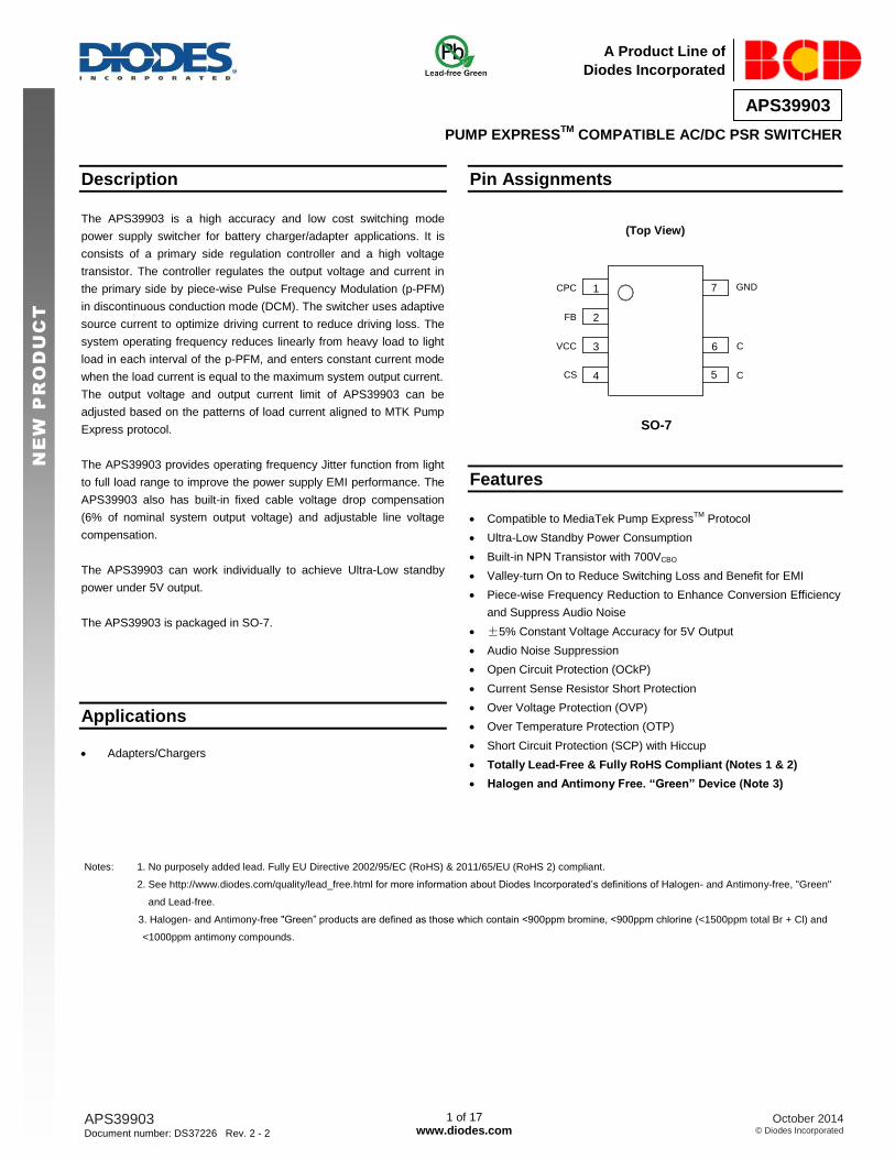
Pin Assignments
(Top View)
1
2
3
4
7
6
5
FB
VCC
GND
C
CCS
CPC
SO-7
Features
Compatible to MediaTek Pump ExpressTM
Protocol
Ultra-Low Standby Power Consumption
Built-in NPN Transistor with 700VCBO
Valley-turn On to Reduce Switching Loss and Benefit for EMI
Piece-wise Frequency Reduction to Enhance Conversion Efficiency
and Suppress Audio Noise
±5% Constant Voltage Accuracy for 5V Output
Audio Noise Suppression
Open Circuit Protection (OCkP)
Current Sense Resistor Short Protection
Over Voltage Protection (OVP)
Over Temperature Protection (OTP)
Short Circuit Protection (SCP) with Hiccup
Totally Lead-Free & Fully RoHS Compliant (Notes 1 & 2)
Halogen and Antimony Free. “Green” Device (Note 3)
Notes: 1. No purposely added lead. Fully EU Directive 2002/95/EC (RoHS) & 2011/65/EU (RoHS 2) compliant.
2. See http://www.diodes.com/quality/lead_free.html for more information about Diodes Incorporated’s definitions of Halogen- and Antimony-free, "Green"
and Lead-free.
3. Halogen- and Antimony-free "Green” products are defined as those which contain <900ppm bromine, <900ppm chlorine (<1500ppm total Br + Cl) and
<1000ppm antimony compounds.
Page 2
APS39903 Document number: DS37226 Rev. 2 - 2
2 of 17 www.diodes.com
October 2014 © Diodes Incorporated
APS39903
A Product Line of
Diodes Incorporated
NE
W P
RO
DU
CT
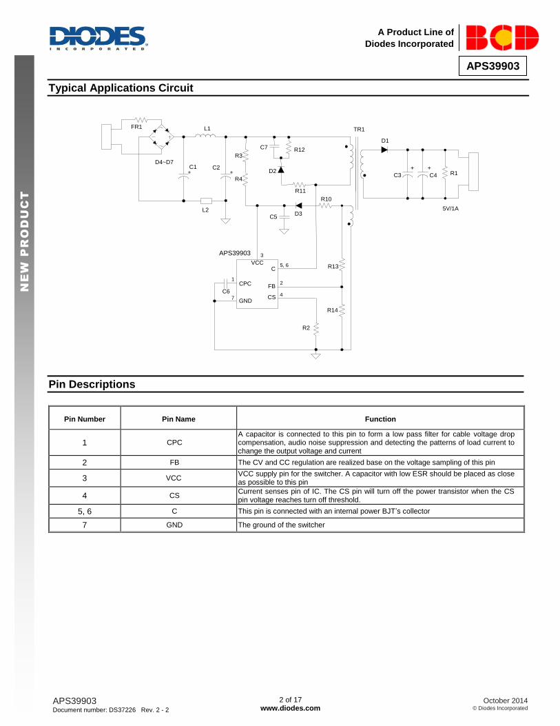
Typical Applications Circuit
+C1
FR1
+C2
L1 TR1
D1
+
FB
R13CVCC
R2
R14
APS39903
CPC
GND
C6
R3
R4
5V/1A
C3
D4~D7
L2
R12C7
D2+
C4
D3C5
R11
CS
R1
R10
7
1
4
2
5, 6
3
Pin Descriptions
Pin Number Pin Name Function
1 CPC A capacitor is connected to this pin to form a low pass filter for cable voltage drop compensation, audio noise suppression and detecting the patterns of load current to change the output voltage and current
2 FB The CV and CC regulation are realized base on the voltage sampling of this pin
3 VCC VCC supply pin for the switcher. A capacitor with low ESR should be placed as close as possible to this pin
4 CS Current senses pin of IC. The CS pin will turn off the power transistor when the CS pin voltage reaches turn off threshold.
5, 6 C This pin is connected with an internal power BJT’s collector
7 GND The ground of the switcher
Page 3
APS39903 Document number: DS37226 Rev. 2 - 2
3 of 17 www.diodes.com
October 2014 © Diodes Incorporated
APS39903
A Product Line of
Diodes Incorporated
NE
W P
RO
DU
CT
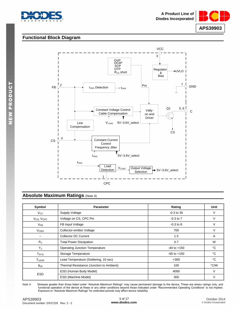
Functional Block Diagram
Regulator&
Bias
OVPOCkP
OTPUVLO
Vally-
on and
Driver
FB
CS
VCC
C
GND
Constant Voltage Control
Cable Compensation
4
3
5, 6
7
1
2
Constant Current
Control
Frequency Jitter
Pro
Line
Compensation
tONStONS Detection
VLOAD
RCS short
SCP
tONS
Load
Detection
CPC
VLOAD Output Voltage
Selection5V~3.6V_select
5V~3.6V_select
5V~3.6V_select
tONS
CS
Q1
Absolute Maximum Ratings (Note 4)
Symbol Parameter Rating Unit
VCC Supply Voltage -0.3 to 35 V
VCS, VCPC Voltage on CS, CPC Pin -0.3 to 7 V
VFB FB Input Voltage -0.3 to 8 V
VCBO Collector-emitter Voltage 700 V
– Collector DC Current 1.5 A
PD Total Power Dissipation 0.7 W
TJ Operating Junction Temperature -40 to +150 °C
TSTG Storage Temperature -65 to +150 °C
TLEAD Lead Temperature (Soldering, 10 sec) +300 °C
θJA Thermal Resistance (Junction to Ambient) 100 °C/W
ESD ESD (Human Body Model) 4000 V
ESD (Machine Model) 300 V
Note 4: Stresses greater than those listed under “Absolute Maximum Ratings” may cause permanent damage to the device. These are stress ratings only, and functional operation of the device at these or any other conditions beyond those indicated under “Recommended Operating Conditions” is not implied. Exposure to “Absolute Maximum Ratings” for extended periods may affect device reliability.
Page 4
APS39903 Document number: DS37226 Rev. 2 - 2
4 of 17 www.diodes.com
October 2014 © Diodes Incorporated
APS39903
A Product Line of
Diodes Incorporated
NE
W P
RO
DU
CT
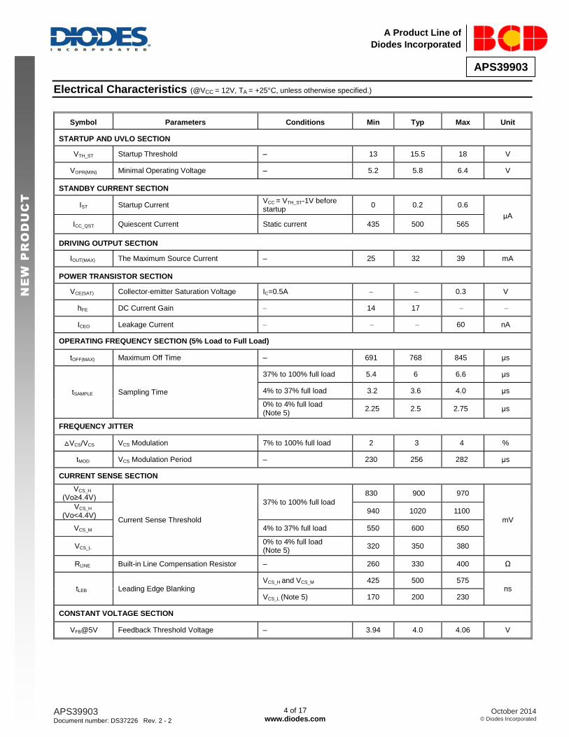
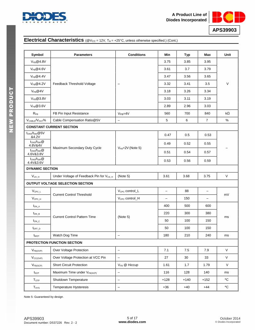
Electrical Characteristics (@VCC = 12V, TA = +25°C, unless otherwise specified.)
Symbol Parameters Conditions Min Typ Max Unit
STARTUP AND UVLO SECTION
VTH_ST Startup Threshold – 13 15.5 18 V
VOPR(MIN) Minimal Operating Voltage – 5.2 5.8 6.4 V
STANDBY CURRENT SECTION
IST Startup Current VCC = VTH_ST-1V before startup
0 0.2 0.6
μA ICC_QST Quiescent Current Static current 435 500 565
DRIVING OUTPUT SECTION
IOUT(MAX) The Maximum Source Current – 25 32 39 mA
POWER TRANSISTOR SECTION
VCE(SAT) Collector-emitter Saturation Voltage IC=0.5A – – 0.3 V
hFE DC Current Gain – 14 17 – –
ICEO Leakage Current – – – 60 nA
OPERATING FREQUENCY SECTION (5% Load to Full Load)
tOFF(MAX) Maximum Off Time – 691 768 845 μs
tSAMPLE Sampling Time
37% to 100% full load 5.4 6 6.6 μs
4% to 37% full load 3.2 3.6 4.0 μs
0% to 4% full load (Note 5)
2.25 2.5 2.75 μs
FREQUENCY JITTER
VCS/VCS VCS Modulation 7% to 100% full load 2 3 4 %
tMOD VCS Modulation Period – 230 256 282 μs
CURRENT SENSE SECTION
VCS_H
(Vo≥4.4V)
Current Sense Threshold
37% to 100% full load
830 900 970
mV
VCS_H
(Vo<4.4V) 940 1020 1100
VCS_M 4% to 37% full load 550 600 650
VCS_L 0% to 4% full load (Note 5)
320 350 380
RLINE Built-in Line Compensation Resistor – 260 330 400 Ω
tLEB Leading Edge Blanking VCS_H and VCS_M 425 500 575
ns VCS_L (Note 5) 170 200 230
CONSTANT VOLTAGE SECTION
VFB@5V Feedback Threshold Voltage – 3.94 4.0 4.06 V
Page 5
APS39903 Document number: DS37226 Rev. 2 - 2
5 of 17 www.diodes.com
October 2014 © Diodes Incorporated
APS39903
A Product Line of
Diodes Incorporated
NE
W P
RO
DU
CT
Electrical Characteristics (@VCC = 12V, TA = +25°C, unless otherwise specified.) (Cont.)
Symbol Parameters Conditions Min Typ Max Unit
[email protected]
Feedback Threshold Voltage –
3.75 3.85 3.95
V
[email protected] 3.61 3.7 3.79
[email protected] 3.47 3.56 3.65
[email protected] 3.32 3.41 3.5
VFB@4V 3.18 3.26 3.34
[email protected] 3.03 3.11 3.19
[email protected] 2.89 2.96 3.03
RFB FB Pin Input Resistance VFB=4V 560 700 840 kΩ
VCABLE/VOUT% Cable Compensation Ratio@5V – 5 6 7 %
CONSTANT CURRENT SECTION
tONS/tSW@5V&4.2V
Maximum Secondary Duty Cycle VFB=2V (Note 5)
0.47 0.5 0.53
–
tONS/[email protected] &4V
0.49 0.52 0.55
tONS/[email protected] &3.8V
0.51 0.54 0.57
tONS/[email protected] &3.6V
0.53 0.56 0.59
DYNAMIC SECTION
VUV_H Under Voltage of Feedback Pin for VCS_H (Note 5) 3.61 3.68 3.75 V
OUTPUT VOLTAGE SELECTION SECTION
VCPC_L Current Control Threshold
VCPC control_L – 88 – mV
VCPC_H VCPC control_H – 150 –
tON_A
Current Control Pattern Time (Note 5)
400 500 600
ms tON_B 220 300 380
tON_C 50 100 150
tOFF_D 50 100 150
tWDT Watch Dog Time – 180 210 240 ms
PROTECTION FUNCTION SECTION
VFB(OVP) Over Voltage Protection – 7.1 7.5 7.9 V
VCC(OVP) Over Voltage Protection at VCC Pin – 27 30 33 V
VFB(SCP) Short Circuit Protection VFB @ Hiccup 1.61 1.7 1.79 V
tSCP Maximum Time under VFB(SCP) – 116 128 140 ms
TOTP Shutdown Temperature – +128 +140 +152 °C
THYS Temperature Hysteresis – +36 +40 +44 °C
Note 5: Guaranteed by design.
Page 6
APS39903 Document number: DS37226 Rev. 2 - 2
6 of 17 www.diodes.com
October 2014 © Diodes Incorporated
APS39903
A Product Line of
Diodes Incorporated
NE
W P
RO
DU
CT
Operation Principle Description
+C1
FR1
+C2
L1 TR1
D1
+
FB
R13CVCC
R2
R14
APS39903
CPC
GND
C6
R3
R4
5V/1A
C3
D4~D7
L2
R12C7
D2+
C4
D3C5
R11
CS
R1
R10
7
1
4
2
5, 6
3
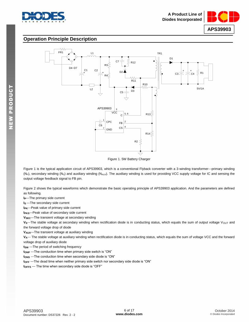
Figure 1. 5W Battery Charger
Figure 1 is the typical application circuit of APS39903, which is a conventional Flyback converter with a 3-winding transformer---primary winding
(NP), secondary winding (NS) and auxiliary winding (NAUX). The auxiliary winding is used for providing VCC supply voltage for IC and sensing the
output voltage feedback signal to FB pin.
Figure 2 shows the typical waveforms which demonstrate the basic operating principle of APS39903 application. And the parameters are defined
as following.
IP---The primary side current
IS ---The secondary side current
IPK---Peak value of primary side current
IPKS---Peak value of secondary side current
VSEC---The transient voltage at secondary winding
VS---The stable voltage at secondary winding when rectification diode is in conducting status, which equals the sum of output voltage VOUT and
the forward voltage drop of diode
VAUX---The transient voltage at auxiliary winding
VA--- The stable voltage at auxiliary winding when rectification diode is in conducting status, which equals the sum of voltage VCC and the forward
voltage drop of auxiliary diode
tSW ---The period of switching frequency
tONP ---The conduction time when primary side switch is “ON”
tONS ---The conduction time when secondary side diode is “ON”
tOFF ---The dead time when neither primary side switch nor secondary side diode is “ON”
tOFFS --- The time when secondary side diode is “OFF”
Page 7
APS39903 Document number: DS37226 Rev. 2 - 2
7 of 17 www.diodes.com
October 2014 © Diodes Incorporated
APS39903
A Product Line of
Diodes Incorporated
NE
W P
RO
DU
CT
Operation Principle Description (Cont.)
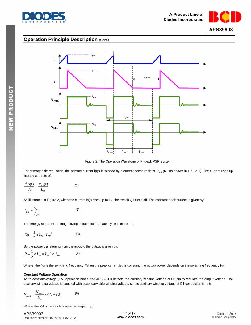
Figure 2. The Operation Waveform of Flyback PSR System
For primary-side regulation, the primary current ip(t) is sensed by a current sense resistor RCS (R2 as shown in Figure 1). The current rises up
linearly at a rate of:
ML
t
dt
tdip )(V)( IN (1)
As illustrated in Figure 2, when the current ip(t) rises up to IPK, the switch Q1 turns off. The constant peak current is given by:
CS
CSPK
R
VI (2)
The energy stored in the magnetizing inductance LM each cycle is therefore:
2
2
1PKM ILEg (3)
So the power transferring from the input to the output is given by:
SWPKM fILP 2
2
1 (4)
Where, the fSW is the switching frequency. When the peak current IPK is constant, the output power depends on the switching frequency fSW.
Constant Voltage Operation
As to constant-voltage (CV) operation mode, the APS39903 detects the auxiliary winding voltage at FB pin to regulate the output voltage. The
auxiliary winding voltage is coupled with secondary side winding voltage, so the auxiliary winding voltage at D1 conduction time is:
VdVoN
NV
S
AUXAUX (5)
Where the Vd is the diode forward voltage drop.
t ONP t ONS
I PK
I PKS
V S
I P
I S t OFFS
t OFF
V SEC
V A V AUX
tSW
Page 8
APS39903 Document number: DS37226 Rev. 2 - 2
8 of 17 www.diodes.com
October 2014 © Diodes Incorporated
APS39903
A Product Line of
Diodes Incorporated
NE
W P
RO
DU
CT
Operation Principle Description (Cont.)
0V
See equation 5
tONS
tSAMPLE
Figure 3. Auxiliary Voltage Waveform
The voltage detection point is at a constant delay time of the D1 on-time. The constant delay time is changed with the different primary peak current. The CV loop control function of APS39903 then generates a D1 off-time to regulate the output voltage.
Constant Current Operation
The APS39903 can work in constant-current (CC) mode. Figure 2 shows the secondary current waveforms.
In CC operation mode, the CC control loop of APS39903 will keep a fixed proportion between D1 on-time tONS and D1 off-time tOFFS. The fixed
proportion is
4
4
OFFS
ONS
t
t (6)
The relationship between the output current and secondary peak current IPKS is given by:
OFFSONS
ONSPKSOUT
tt
tII
2
1 (7)
As to tight coupled primary and secondary winding, the secondary peak current is
PK
S
PPKS I
N
NI (8)
Thus the output constant-current is given by:
PK
S
P
OFFSONS
ONSPK
S
POUT I
N
N
tt
tI
N
NI
8
2
2
1 (9)
Therefore, APS39903 can realize CC mode operation by constant primary peak current and fixed diode conduction duty cycle. Multiple Segment Constant Peak Current
As to the original PFM PSR system, the switching frequency decreases with output current decreasing, which will encounter audible noise issue
since switching frequency decreases to audio frequency range, about less than 20kHz.
In order to avoid audible noise issue, APS39903 uses 3-segment constant primary peak current control method. At constant voltage mode, the
current sense threshold voltage is multiple segment with different loading, as shown in Figure 4, which are VCS_H for high load, VCS_M for
medium load and VCS_L for light load. At constant current mode, the peak current is still VCS_H.
Page 9
APS39903 Document number: DS37226 Rev. 2 - 2
9 of 17 www.diodes.com
October 2014 © Diodes Incorporated
APS39903
A Product Line of
Diodes Incorporated
NE
W P
RO
DU
CT
Operation Principle Description (Cont.)
IOMAX
VCS_L
VCS_M
VCS_H
Light Load
Medium Load
High Load
VCS_REF
IOMAX
fsw
22kHz
2kHz
60kHz
37%4% 100%
12kHz
4kHz
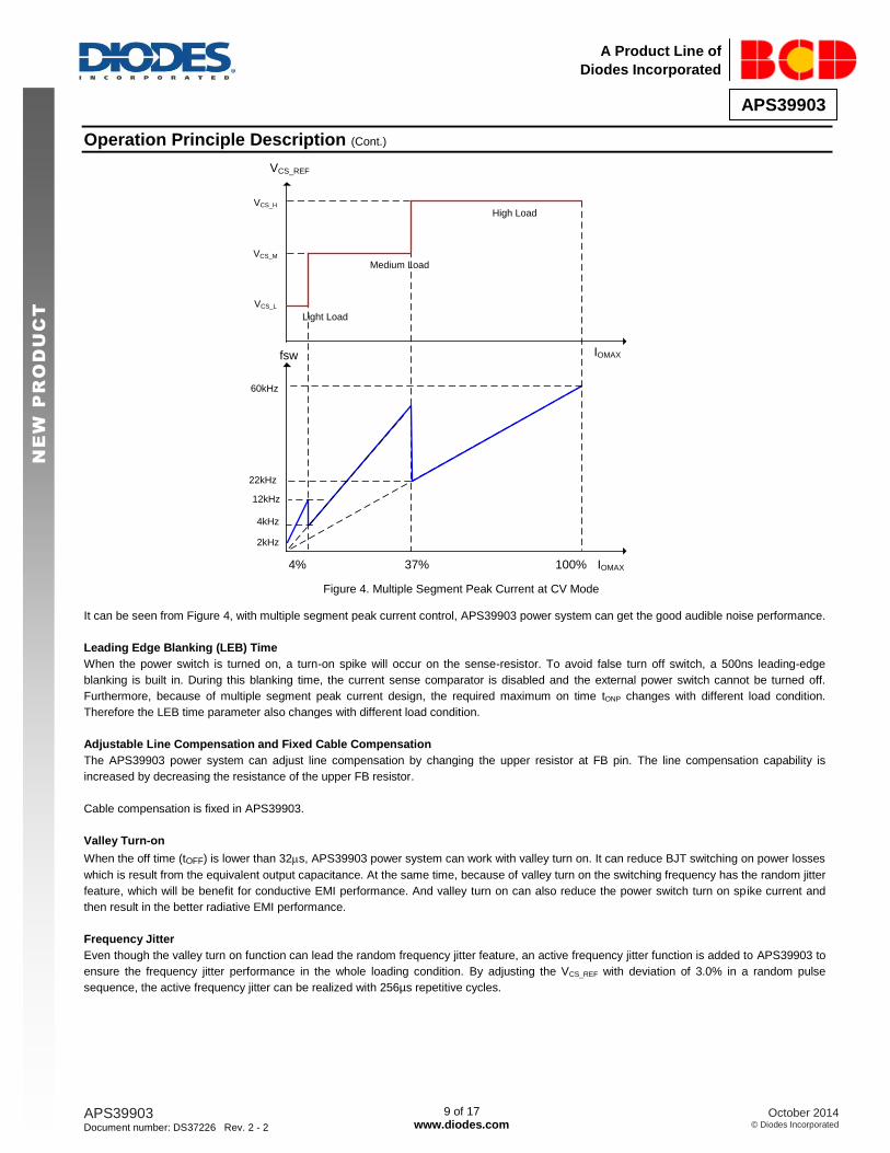
Figure 4. Multiple Segment Peak Current at CV Mode
It can be seen from Figure 4, with multiple segment peak current control, APS39903 power system can get the good audible noise performance.
Leading Edge Blanking (LEB) Time
When the power switch is turned on, a turn-on spike will occur on the sense-resistor. To avoid false turn off switch, a 500ns leading-edge
blanking is built in. During this blanking time, the current sense comparator is disabled and the external power switch cannot be turned off.
Furthermore, because of multiple segment peak current design, the required maximum on time tONP changes with different load condition.
Therefore the LEB time parameter also changes with different load condition.
Adjustable Line Compensation and Fixed Cable Compensation
The APS39903 power system can adjust line compensation by changing the upper resistor at FB pin. The line compensation capability is
increased by decreasing the resistance of the upper FB resistor.
Cable compensation is fixed in APS39903.
Valley Turn-on
When the off time (tOFF) is lower than 32s, APS39903 power system can work with valley turn on. It can reduce BJT switching on power losses
which is result from the equivalent output capacitance. At the same time, because of valley turn on the switching frequency has the random jitter
feature, which will be benefit for conductive EMI performance. And valley turn on can also reduce the power switch turn on spike current and
then result in the better radiative EMI performance.
Frequency Jitter
Even though the valley turn on function can lead the random frequency jitter feature, an active frequency jitter function is added to APS39903 to
ensure the frequency jitter performance in the whole loading condition. By adjusting the VCS_REF with deviation of 3.0% in a random pulse
sequence, the active frequency jitter can be realized with 256µs repetitive cycles.
Page 10
APS39903 Document number: DS37226 Rev. 2 - 2
10 of 17 www.diodes.com
October 2014 © Diodes Incorporated
APS39903
A Product Line of
Diodes Incorporated
NE
W P
RO
DU
CT
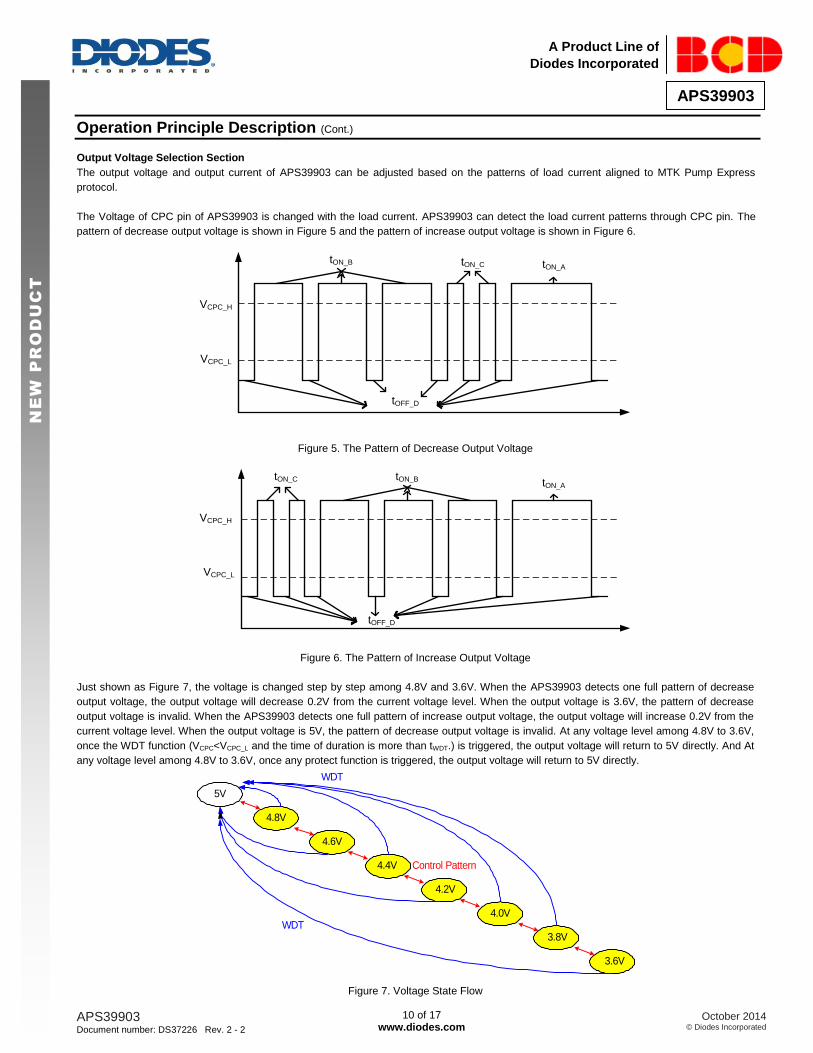
Operation Principle Description (Cont.) Output Voltage Selection Section
The output voltage and output current of APS39903 can be adjusted based on the patterns of load current aligned to MTK Pump Express
protocol.
The Voltage of CPC pin of APS39903 is changed with the load current. APS39903 can detect the load current patterns through CPC pin. The
pattern of decrease output voltage is shown in Figure 5 and the pattern of increase output voltage is shown in Figure 6.
VCPC_L
VCPC_H
tON_B tON_C tON_A
tOFF_D
Figure 5. The Pattern of Decrease Output Voltage
tON_AtON_BtON_C
tOFF_D
VCPC_L
VCPC_H
Figure 6. The Pattern of Increase Output Voltage
Just shown as Figure 7, the voltage is changed step by step among 4.8V and 3.6V. When the APS39903 detects one full pattern of decrease
output voltage, the output voltage will decrease 0.2V from the current voltage level. When the output voltage is 3.6V, the pattern of decrease
output voltage is invalid. When the APS39903 detects one full pattern of increase output voltage, the output voltage will increase 0.2V from the
current voltage level. When the output voltage is 5V, the pattern of decrease output voltage is invalid. At any voltage level among 4.8V to 3.6V,
once the WDT function (VCPC<VCPC_L and the time of duration is more than tWDT.) is triggered, the output voltage will return to 5V directly. And At
any voltage level among 4.8V to 3.6V, once any protect function is triggered, the output voltage will return to 5V directly.
Figure 7. Voltage State Flow
5V
4.8V
4.6V
4.4V
4.2V
4.0V
3.8V
3.6V
WDT
WDT
Control Pattern
Page 11
APS39903 Document number: DS37226 Rev. 2 - 2
11 of 17 www.diodes.com
October 2014 © Diodes Incorporated
APS39903
A Product Line of
Diodes Incorporated
NE
W P
RO
DU
CT
Operation Principle Description (Cont.)
CCM Protection
The APS39903 is designed to operate in discontinuous conduction mode (DCM) in both CV and CC modes. To avoid operating in continuous
conduction mode (CCM), the APS39903 detects the falling edge of the FB input voltage on each cycle. If a 0V falling edge of FB is not detected,
the APS39903 stops working.
OVP & OCkP
The APS39903 includes output over-voltage protection (OVP) and open circuit protection (OCkP) circuitry. If the voltage at FB pin exceeds 7.5V,
90% above the normal detection voltage, or the 0V falling edge of the FB input can’t be monitored, the APS39903 immediately shuts down and
keeps the internal circuitry enabled to discharge the VCC capacitor to the UVLO turn-off threshold. After that, the device returns to the start
state and a start-up sequence ensues.
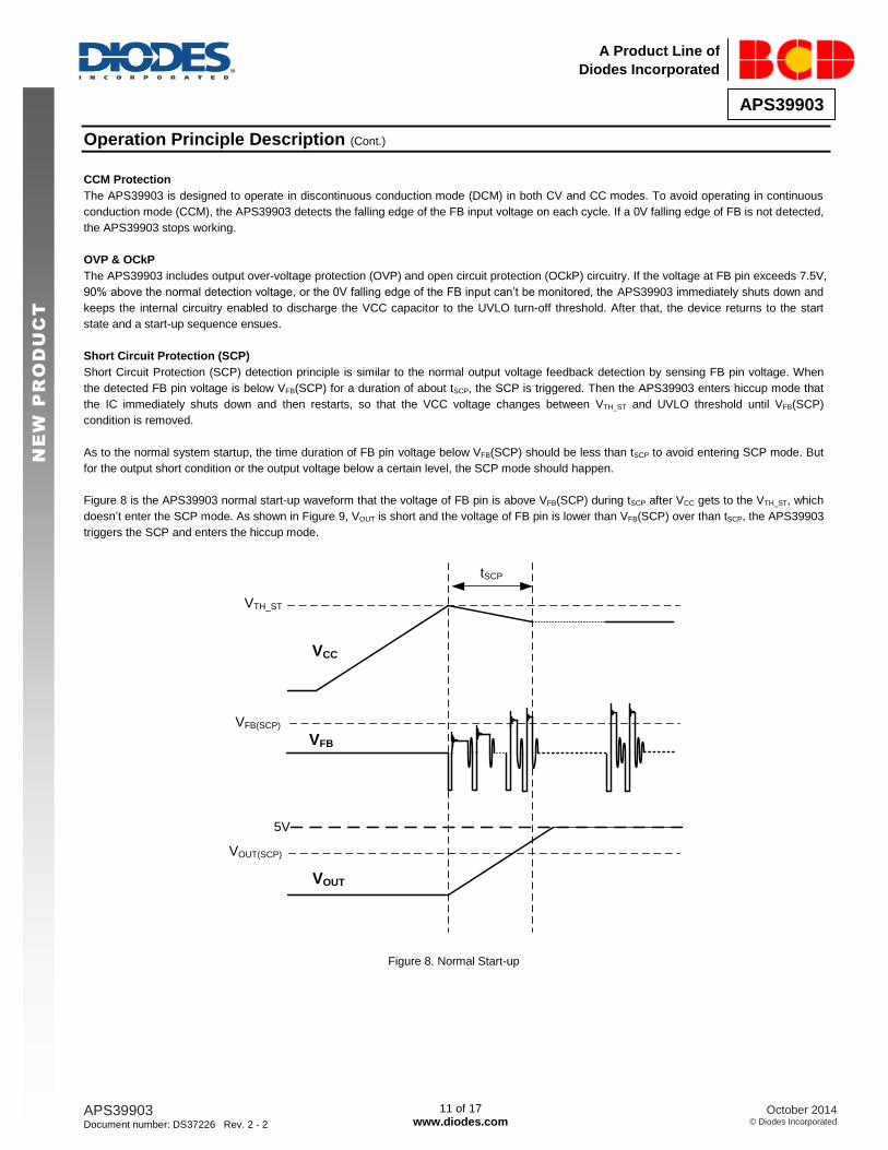
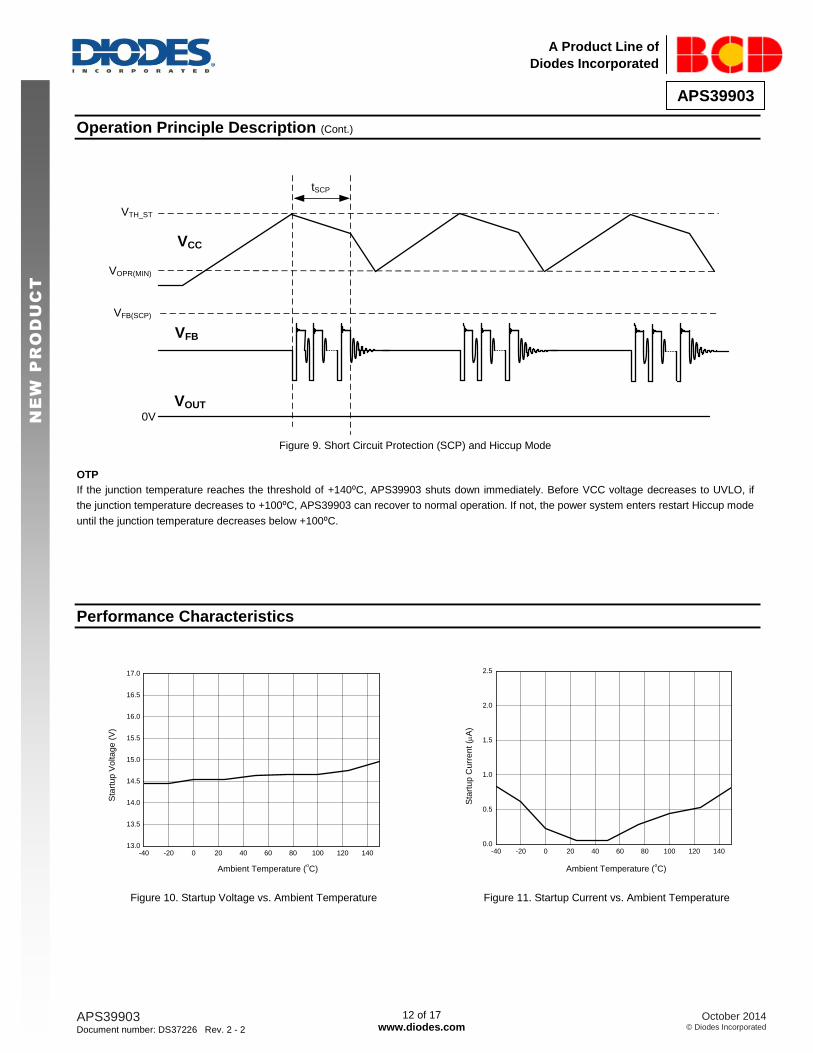
Short Circuit Protection (SCP)
Short Circuit Protection (SCP) detection principle is similar to the normal output voltage feedback detection by sensing FB pin voltage. When
the detected FB pin voltage is below VFB(SCP) for a duration of about tSCP, the SCP is triggered. Then the APS39903 enters hiccup mode that
the IC immediately shuts down and then restarts, so that the VCC voltage changes between VTH_ST and UVLO threshold until VFB(SCP)
condition is removed.
As to the normal system startup, the time duration of FB pin voltage below VFB(SCP) should be less than tSCP to avoid entering SCP mode. But
for the output short condition or the output voltage below a certain level, the SCP mode should happen.
Figure 8 is the APS39903 normal start-up waveform that the voltage of FB pin is above VFB(SCP) during tSCP after VCC gets to the VTH_ST, which
doesn’t enter the SCP mode. As shown in Figure 9, VOUT is short and the voltage of FB pin is lower than VFB(SCP) over than tSCP, the APS39903
triggers the SCP and enters the hiccup mode.
VTH_ST
VFB(SCP)
tSCP
VCC
VFB
VOUT
VOUT(SCP)
5V
Figure 8. Normal Start-up
Page 12
APS39903 Document number: DS37226 Rev. 2 - 2
12 of 17 www.diodes.com
October 2014 © Diodes Incorporated
APS39903
A Product Line of
Diodes Incorporated
NE
W P
RO
DU
CT
Operation Principle Description (Cont.)
VTH_ST
VOPR(MIN)
VFB(SCP)
tSCP
VCC
VFB
VOUT
0V
Figure 9. Short Circuit Protection (SCP) and Hiccup Mode
OTP
If the junction temperature reaches the threshold of +140⁰C, APS39903 shuts down immediately. Before VCC voltage decreases to UVLO, if
the junction temperature decreases to +100⁰C, APS39903 can recover to normal operation. If not, the power system enters restart Hiccup mode
until the junction temperature decreases below +100⁰C.
Performance Characteristics
-40 -20 0 20 40 60 80 100 120 14013.0
13.5
14.0
14.5
15.0
15.5
16.0
16.5
17.0
Ambient Temperature (oC)
Sta
rtu
p V
olta
ge
(V
)
-40 -20 0 20 40 60 80 100 120 1400.0
0.5
1.0
1.5
2.0
2.5
Sta
rtu
p C
urr
en
t (
A)
Ambient Temperature (oC)
Figure 10. Startup Voltage vs. Ambient Temperature Figure 11. Startup Current vs. Ambient Temperature
Page 13
APS39903 Document number: DS37226 Rev. 2 - 2
13 of 17 www.diodes.com
October 2014 © Diodes Incorporated
APS39903
A Product Line of
Diodes Incorporated
NE
W P
RO
DU
CT
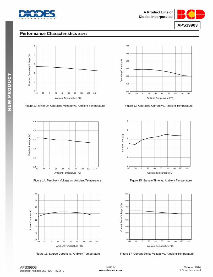
Performance Characteristics (Cont.)
-40 -20 0 20 40 60 80 100 120 1403
4
5
6
7
8
Ambient Temperature (
oC)
Min
imu
m O
pe
ratin
g V
olta
ge
(V
)
-40 -20 0 20 40 60 80 100 120 140400
450
500
550
600
650
700
Ambient Temperature (
oC)
Op
era
tin
g C
urr
en
t (
A)
Figure 12. Minimum Operating Voltage vs. Ambient Temperature Figure 13. Operating Current vs. Ambient Temperature
-40 -20 0 20 40 60 80 100 120 1403.4
3.6
3.8
4.0
4.2
4.4
Fe
ed
ba
ck V
olta
ge
(V
)
Ambient Temperature (oC)
-40 -20 0 20 40 60 80 100 120 1404
5
6
7
8
9
Sa
mp
le T
ime
(s)
Ambient Temperature (oC)
Figure 14. Feedback Voltage vs. Ambient Temperature Figure 15. Sample Time vs. Ambient Temperature
-40 -20 0 20 40 60 80 100 120 14016
18
20
22
24
26
28
30
Ambient Temperature (oC)
So
urc
e C
urr
en
t (m
A)
-40 -20 0 20 40 60 80 100 120 140200
300
400
500
600
700
800
900
Cu
rre
nt S
en
se
Vo
lta
ge
(m
V)
Ambient Temperature (oC)
Figure 16. Source Current vs. Ambient Temperature Figure 17. Current Sense Voltage vs. Ambient Temperature
Page 14
APS39903 Document number: DS37226 Rev. 2 - 2
14 of 17 www.diodes.com
October 2014 © Diodes Incorporated
APS39903
A Product Line of
Diodes Incorporated
NE
W P
RO
DU
CT
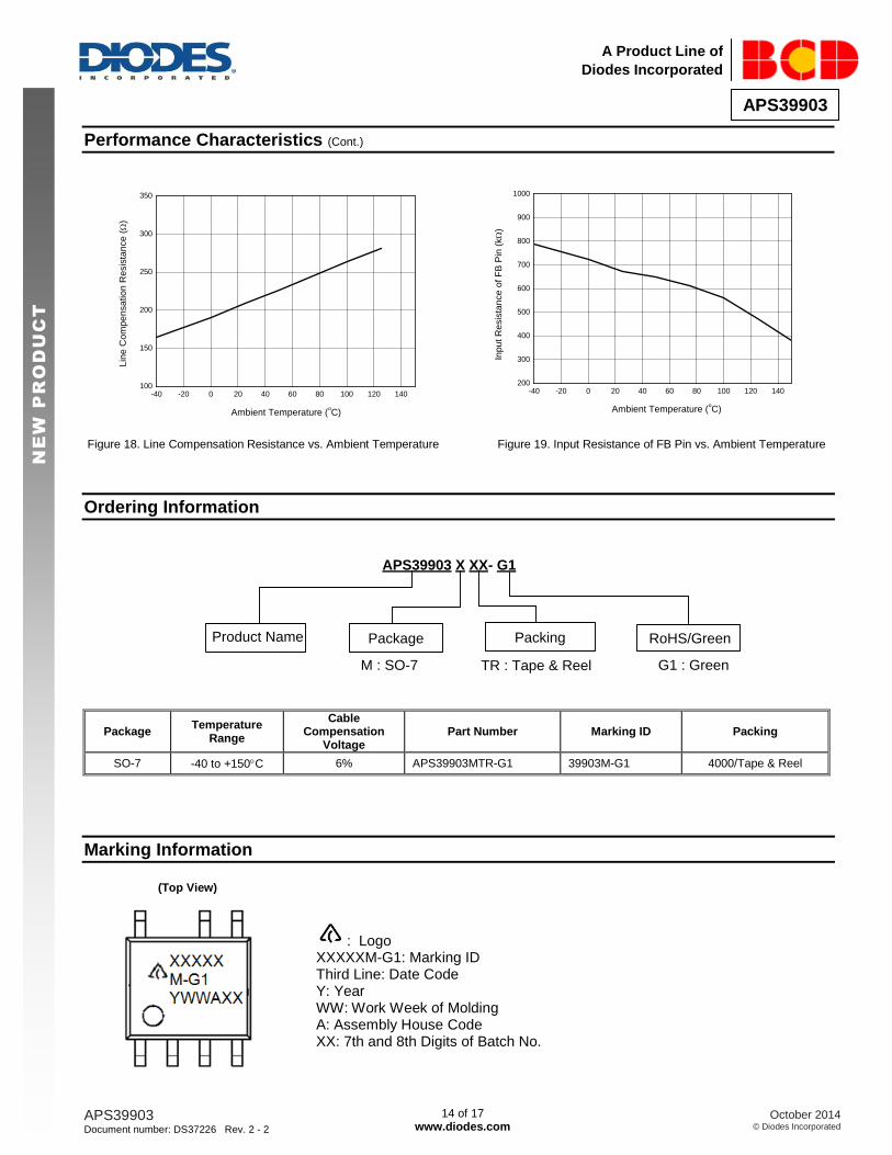
Performance Characteristics (Cont.)
-40 -20 0 20 40 60 80 100 120 140100
150
200
250
300
350
Ambient Temperature (oC)
Lin
e C
om
pe
nsatio
n R
esis
tan
ce (
)
Figure 18. Line Compensation Resistance vs. Ambient Temperature Figure 19. Input Resistance of FB Pin vs. Ambient Temperature
Ordering Information
APS39903 X XX- G1
PackingPackage
TR : Tape & ReelM : SO-7 G1 : Green
Product Name RoHS/Green
Package Temperature
Range
Cable Compensation
Voltage Part Number Marking ID Packing
SO-7 -40 to +150C 6% APS39903MTR-G1 39903M-G1 4000/Tape & Reel
Marking Information
(Top View)
: Logo XXXXXM-G1: Marking ID Third Line: Date Code Y: Year WW: Work Week of Molding A: Assembly House Code XX: 7th and 8th Digits of Batch No.
-40 -20 0 20 40 60 80 100 120 140200
300
400
500
600
700
800
900
1000
Ambient Temperature (oC)
Inp
ut R
esis
tan
ce
of F
B P
in (
k
)
Page 15
APS39903 Document number: DS37226 Rev. 2 - 2
15 of 17 www.diodes.com
October 2014 © Diodes Incorporated
APS39903
A Product Line of
Diodes Incorporated
NE
W P
RO
DU
CT
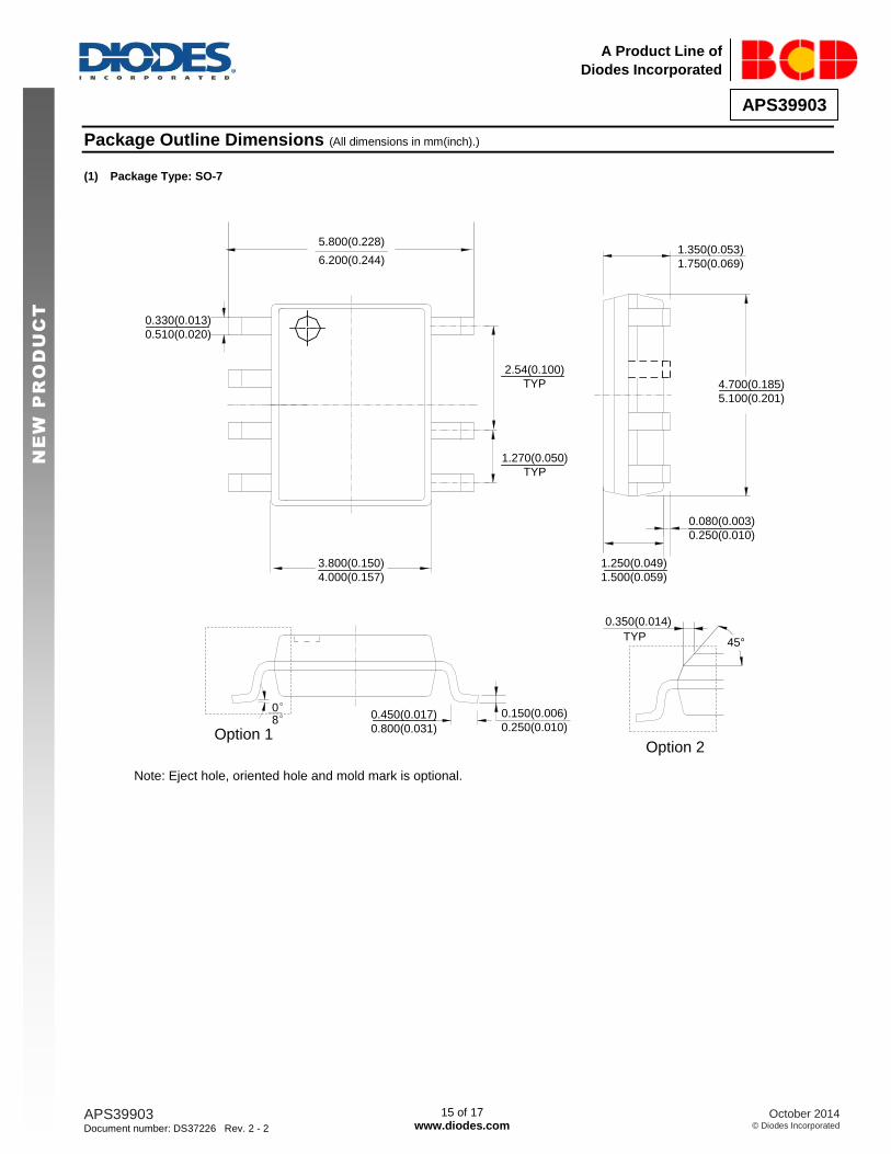
Package Outline Dimensions (All dimensions in mm(inch).)
(1) Package Type: SO-7
3.800(0.150)
4.000(0.157)
1.270(0.050)
TYP
4.700(0.185)
5.100(0.201)
0.330(0.013)
0.510(0.020)
0.150(0.006)
0.250(0.010)
0.080(0.003)
0.250(0.010)
1.350(0.053)
1.750(0.069)
0.450(0.017)
0.800(0.031)8°0°
5.800(0.228)
6.200(0.244)
2.54(0.100)
TYP
1.250(0.049)
1.500(0.059)
Note: Eject hole, oriented hole and mold mark is optional.
Option 2
45°
0.350(0.014)
TYP
Option 1
Page 16
APS39903 Document number: DS37226 Rev. 2 - 2
16 of 17 www.diodes.com
October 2014 © Diodes Incorporated
APS39903
A Product Line of
Diodes Incorporated
NE
W P
RO
DU
CT
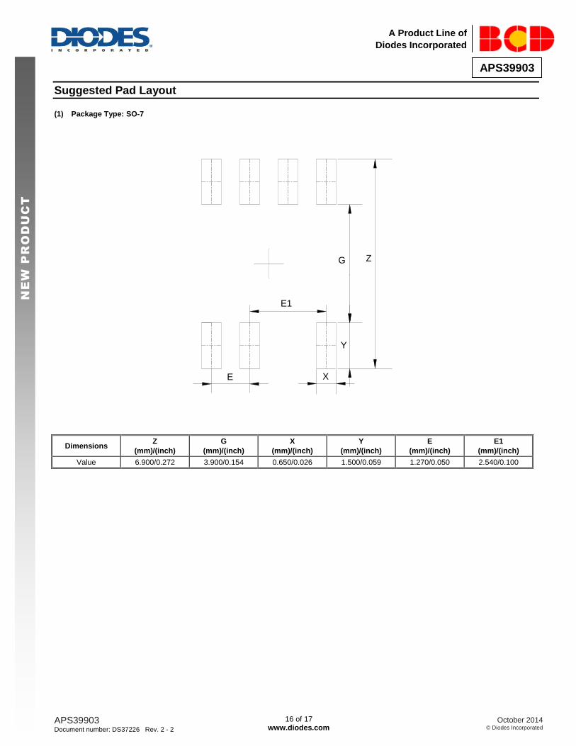
Suggested Pad Layout
(1) Package Type: SO-7
ZG
E1
E X
Y
Dimensions Z
(mm)/(inch)
G
(mm)/(inch)
X
(mm)/(inch)
Y
(mm)/(inch)
E
(mm)/(inch)
E1
(mm)/(inch)
Value 6.900/0.272 3.900/0.154 0.650/0.026 1.500/0.059 1.270/0.050 2.540/0.100
Page 17
APS39903 Document number: DS37226 Rev. 2 - 2
17 of 17 www.diodes.com
October 2014 © Diodes Incorporated
APS39903
A Product Line of
Diodes Incorporated
NE
W P
RO
DU
CT
IMPORTANT NOTICE DIODES INCORPORATED MAKES NO WARRANTY OF ANY KIND, EXPRESS OR IMPLIED, WITH REGARDS TO THIS DOCUMENT, INCLUDING, BUT NOT LIMITED TO, THE IMPLIED WARRANTIES OF MERCHANTABILITY AND FITNESS FOR A PARTICULAR PURPOSE (AND THEIR EQUIVALENTS UNDER THE LAWS OF ANY JURISDICTION). Diodes Incorporated and its subsidiaries reserve the right to make modifications, enhancements, improvements, corrections or other changes without further notice to this document and any product described herein. Diodes Incorporated does not assume any liability arising out of the application or use of this document or any product described herein; neither does Diodes Incorporated convey any license under its patent or trademark rights, nor the rights of others. Any Customer or user of this document or products described herein in such applications shall assume all risks of such use and will agree to hold Diodes Incorporated and all the companies whose products are represented on Diodes Incorporated website, harmless against all damages. Diodes Incorporated does not warrant or accept any liability whatsoever in respect of any products purchased through unauthorized sales channel. Should Customers purchase or use Diodes Incorporated products for any unintended or unauthorized application, Customers shall indemnify and hold Diodes Incorporated and its representatives harmless against all claims, damages, expenses, and attorney fees arising out of, directly or indirectly, any claim of personal injury or death associated with such unintended or unauthorized application. Products described herein may be covered by one or more United States, international or foreign patents pending. Product names and markings noted herein may also be covered by one or more United States, international or foreign trademarks. This document is written in English but may be translated into multiple languages for reference. Only the English version of this document is the final and determinative format released by Diodes Incorporated.
LIFE SUPPORT Diodes Incorporated products are specifically not authorized for use as critical components in life support devices or systems without the express written approval of the Chief Executive Officer of Diodes Incorporated. As used herein: A. Life support devices or systems are devices or systems which: 1. are intended to implant into the body, or
2. support or sustain life and whose failure to perform when properly used in accordance with instructions for use provided in the labeling can be reasonably expected to result in significant injury to the user.
B. A critical component is any component in a life support device or system whose failure to perform can be reasonably expected to cause the failure of the life support device or to affect its safety or effectiveness. Customers represent that they have all necessary expertise in the safety and regulatory ramifications of their life support devices or systems, and acknowledge and agree that they are solely responsible for all legal, regulatory and safety-related requirements concerning their products and any use of Diodes Incorporated products in such safety-critical, life support devices or systems, notwithstanding any devices- or systems-related information or support that may be provided by Diodes Incorporated. Further, Customers must fully indemnify Diodes Incorporated and its representatives against any damages arising out of the use of Diodes Incorporated products in such safety-critical, life support devices or systems. Copyright © 2014, Diodes Incorporated www.diodes.com