© 2018 JETIR October 2018, Volume 5, Issue 10 www.jetir.org (ISSN-2349-5162)
JETIR1810845 Journal of Emerging Technologies and Innovative Research (JETIR) www.jetir.org 437
Design And Implementation of Convolutional Encoder
And Viterbi Decoder On FPGA Sriram.T.K, Rahul Ch
Student, Student, Student
Electronics and Communication Engineering.,
Chaitanya Bharathi Institute of Technology, Hyderabad, India
________________________________________________________________________________________________________
Abstract— The availability of wireless technology has revolutionized the way communication is done in the present scenario. With this
increased accessibility comes increased dependence on the underlying systems to transmit information both quickly and accurately. Because
the communications channels in ‘wireless’ systems can introduce more errors than in “wired” systems, voice and data must use forward error
correction coding to reduce the probability of channel effects corrupting the information being transmitted. One such code which is based on
the forward error correction (FEC) technique is the convolutional code. Convolutional codes can be defined as a set of block codes with
memory where the ‘n’ encoder outputs at any given point of time not only depends on ‘k’ inputs but also depends on ‘m’ memory elements.
The optimum decoding algorithm used for decoding the convolutional codes is the Viterbi algorithm. It is limited to smaller constraint lengths
but it has a greater advantage of using maximum likelihood decoding. Though various platforms can be used for realizing this implementation,
we consider that using an FPGA is advantageous. FPGAs are a technology that gives the designer flexibility of a programmable solution,
minimize the overall cost and enhance the adaptability with optimal device utilization by conserving both board space and system power. In
this project, the Viterbi algorithm is being implemented on an FPGA, Xilinx Spartan 6 XC6SLX45, on designing platform Xilinx ISE design
Suite 14.5 and ChipScope Pro to decode error control codes that are used to enhance the performance of digital communication system by
reducing the probability of channel effects.
Index Terms— Convolutional Codes, FPGA, Wireless Systems, Viterbi Algorithm, Xilinx Spartan 6 ________________________________________________________________________________________________________
I. INTRODUCTION
Objective:
The main aim of this project is FPGA implementation of the convolutional encoder and Viterbi decoder which will allow the receiver
to detect and correct any errors without the need of retransmission. The Convolutional Encoder and the maximum likelihood Viterbi decoder
solve the problem of the transmission of data in an erroneous channel. This project is aimed at designing and implementing the encoder and
decoder on an FPGA so that the receiver can detect and correct any errors without the need of retransmission.
Problem Statement:
Besides the attenuation of the signal in the long distance transmission, every communication channel is exposed to different kinds of
noise sources such as the Anti-White Gaussian noise (AWGN) which fluctuates the voltage around the threshold. The real problem arises
when you discover that the received data has been corrupted and you have to retransmit the whole data again. However, retransmission is
not efficient as it wastes a lot of time and this is not acceptable in applications especially with the advanced communication systems which
have very high data rate. Therefore, there is a need to efficiently transmit data without the need of retransmission.
Contributions
The contributions of this work are as follows:
Design a convolution encoder of rate = ½ and constraint length = 3.
Design a Viterbi Decoder and implement it on an FPGA so that there is no need of retransmission.
II. SYSTEM DESIGN
Architecture
Fig 1:Block Diagram of a Communication System
© 2018 JETIR October 2018, Volume 5, Issue 10 www.jetir.org (ISSN-2349-5162)
JETIR1810845 Journal of Emerging Technologies and Innovative Research (JETIR) www.jetir.org 438
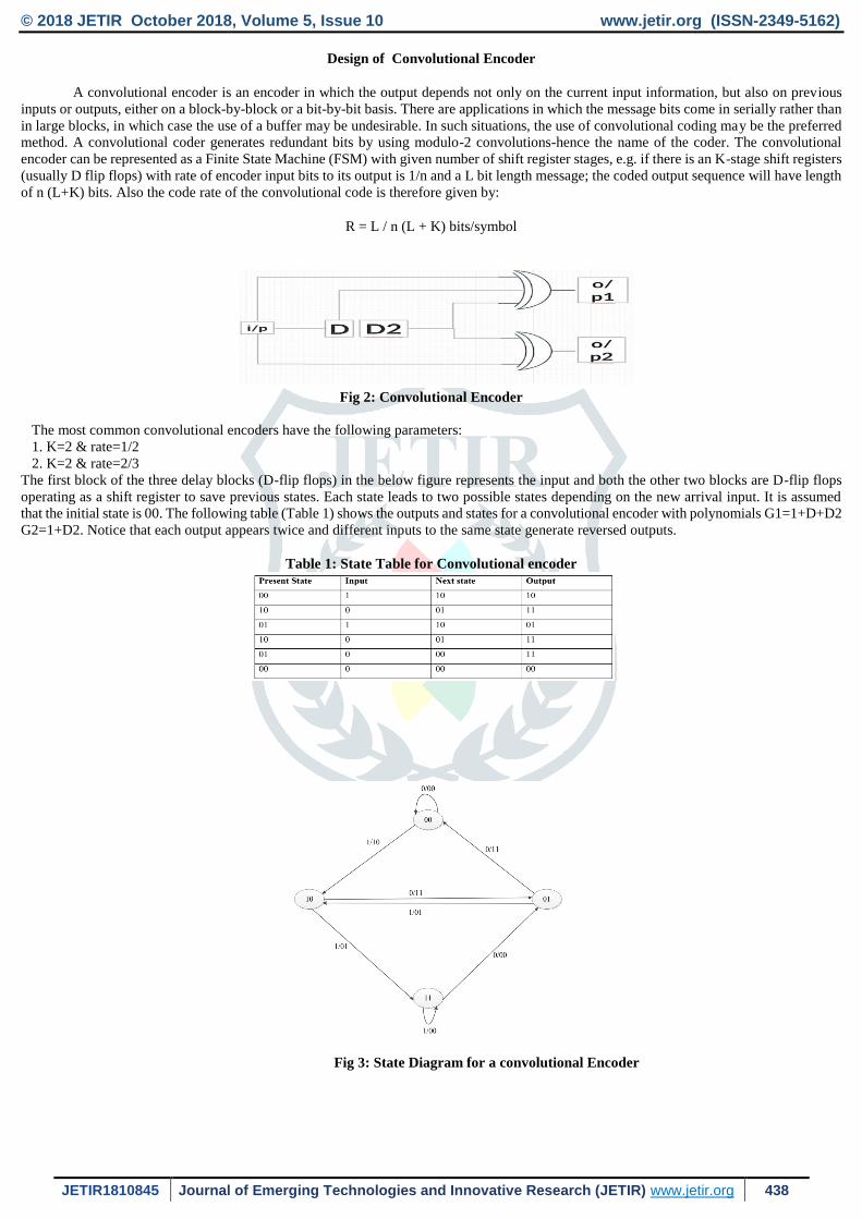
Design of Convolutional Encoder
A convolutional encoder is an encoder in which the output depends not only on the current input information, but also on previous
inputs or outputs, either on a block-by-block or a bit-by-bit basis. There are applications in which the message bits come in serially rather than
in large blocks, in which case the use of a buffer may be undesirable. In such situations, the use of convolutional coding may be the preferred
method. A convolutional coder generates redundant bits by using modulo-2 convolutions-hence the name of the coder. The convolutional
encoder can be represented as a Finite State Machine (FSM) with given number of shift register stages, e.g. if there is an K-stage shift registers
(usually D flip flops) with rate of encoder input bits to its output is 1/n and a L bit length message; the coded output sequence will have length
of n (L+K) bits. Also the code rate of the convolutional code is therefore given by:
R = L / n (L + K) bits/symbol
Fig 2: Convolutional Encoder
The most common convolutional encoders have the following parameters:
1. K=2 & rate=1/2
2. K=2 & rate=2/3
The first block of the three delay blocks (D-flip flops) in the below figure represents the input and both the other two blocks are D-flip flops
operating as a shift register to save previous states. Each state leads to two possible states depending on the new arrival input. It is assumed
that the initial state is 00. The following table (Table 1) shows the outputs and states for a convolutional encoder with polynomials G1=1+D+D2
G2=1+D2. Notice that each output appears twice and different inputs to the same state generate reversed outputs.
Table 1: State Table for Convolutional encoder
Fig 3: State Diagram for a convolutional Encoder
© 2018 JETIR October 2018, Volume 5, Issue 10 www.jetir.org (ISSN-2349-5162)
JETIR1810845 Journal of Emerging Technologies and Innovative Research (JETIR) www.jetir.org 439
Design of a Viterbi Decoder:
An efficient solution to the decoding problem is a dynamic programming algorithm known as the Viterbi algorithm, also known as
the Viterbi Decoder (VD). A Viterbi decoder uses the Viterbi algorithm for decoding a bit stream that has been encoded using convolutional
code or trellis code.The likelihood of a received sequence Ŕ after transmission over a noisy memory less channel for the transmitted coded
sequence Ṽ is the basis in this type of decoding. Viterbi Decoder is a maximum likelihood decoder, in the sense that it finds the closest coded
sequence ṽ to the received sequence ŕ by processing the sequences on a bit-by-bit (branches of the trellis) basis. In other words, instead of
keeping a score of each possible coded sequence, it tracks the states of the trellis.
Fig 4 : Block Diagram of Viterbi Decoder
Fig 5: Trellis Diagram
Fig .6: Survivor Path
© 2018 JETIR October 2018, Volume 5, Issue 10 www.jetir.org (ISSN-2349-5162)
JETIR1810845 Journal of Emerging Technologies and Innovative Research (JETIR) www.jetir.org 440
III: IMPLEMENTATION:
Hardware and Software Tools
Hardware tool used for this project is ATLYS SPARTAN 6 FPGA DEVELOPMEN BOARD. Software tool used for this project is
Xilinx ISE Design Suite 14.5ATLYS SPARTAN 6 FPGA Development Board
In this project we are using Xilinx Spartan 6 XC6SLX45 FPGA package no 3CG324 with speed grade -3. The large FPGA and on-
board collection of high-end peripherals including Gbit Ethernet, HDMI Video, 128MByte 16-bit DDR2 memory, and USB and audio ports
make the Atlys board an ideal host for a wide range of digital systems, including embedded processor designs based on Xilinx’s MicroBlaze.
Atlys is compatible with all Xilinx CAD tools, including ChipScope, so designs can be completed at no extra cost.
Table 2 : No of components used in Convolutional encoder and Viterbi Decoder Combined System.
Design Entry Using Xilinx ISE Design Suite:
In the design entry process, the behavior of circuit is written in hardware description language like VERILOG. Simulation and
synthesis are the two main kinds of tools, which operate on the VERILOG language.
ChipScope Pro Analyzer
Before generating the bit stream file we have to add chip scope pro cores to topmost module and then generate the bit stream file.
Chip Scope Pro allows you to embed the following cores within your design, which assist with on-chip debugging: integrated logic analyzer
(ILA), integrated bus analyzer (IBA), and virtual input/output (VIO) low-profile software cores. For debugging purpose cores which are to be
added can be integrated controller core (ICON) or ILA core or IBA core and virtual input/output core.
The Convolutional Encoder consists of the units ‘rs’, ‘sd’, ‘opshifter’ and ‘fde’.The ‘rs’ unit takes the 6 bit input and transfers it bit by bit to
the ‘sd’ unit. The ‘sd’ unit then gives the 2 bit output corresponding to the input and sends these 2 bits to the ‘opshifter’ unit which inturn acts
like a shift register shifting two bits to the right at a time. The ‘fde’ unit gives the encoded output through the wire ‘op’ once all the encoded
bots have been received from the ‘opshifter’ unit.
Fig 7: RTL Schematic of Convolutional Encoder
The Viterbi Decoder consists of the units ‘bmu’ and ‘acs’. The ‘bmu’ unit is the branch metric unit which calculates the branch metric
for all the branches in the trellis diagtram corresponding to the Viterbi decoder. The ‘acs’ unit is the add, compare and select unit that selects
the branch with the smallest possible metric reaching every node in the Trellis diagram. The ‘acs’ unit also consists of the trace back unit that
calculates the survivor path and the corresponding decoded output.
© 2018 JETIR October 2018, Volume 5, Issue 10 www.jetir.org (ISSN-2349-5162)
JETIR1810845 Journal of Emerging Technologies and Innovative Research (JETIR) www.jetir.org 441
Fig 8: RTL Schematic of Viterbi Decoder
IV: RESULTS
The Simulation result of encoder has a rate that is equal to 1⁄2 that is for one bit of input there are two bits of output. The input is
given to the encoder through the wire ‘ip’ and the output is obtained through the wire ‘op’. The input given in the above case is 6 bit binary
value ‘100100’ and the output so obtained is 12 bit binary value ‘101111101111’.
Fig 9: Simulation Result of Convolutional Encoder
This ChipScope Pro result consists of the waveform generated by the ILA and the output of the VIO console. The input is given through the
VIO console signal ‘encoder in’ and the output is obtained through the signal ‘encoder out’. The input given in the above case is the hexadecimal
value ‘24’ which is equivalent to the binary value ‘100100’ and the output obtained is the hexadecimal value ‘BEF’ which is equivalent to the
binary value ‘101111101111’.The same output can also be seen as the ‘encoder out’ signal in the ILA waveform.
Fig 10: ChipScopePro of Convolutional Encoder
The simulation result of the Viterbi Decoder The encoder has a rate that is equal to 1⁄2, therefore the decoder will give one bit of output for
every two bits of input. The input is given to the decoder through the wire ‘in1’ and the output is obtained through the wire ‘do1’. The input
given in the above case is 12 bit binary value ‘101111101111’ and the output so obtained is 6 bit binary value ‘100100’.
Fig 11: Simulation Result of Viterbi Decoder
© 2018 JETIR October 2018, Volume 5, Issue 10 www.jetir.org (ISSN-2349-5162)
JETIR1810845 Journal of Emerging Technologies and Innovative Research (JETIR) www.jetir.org 442
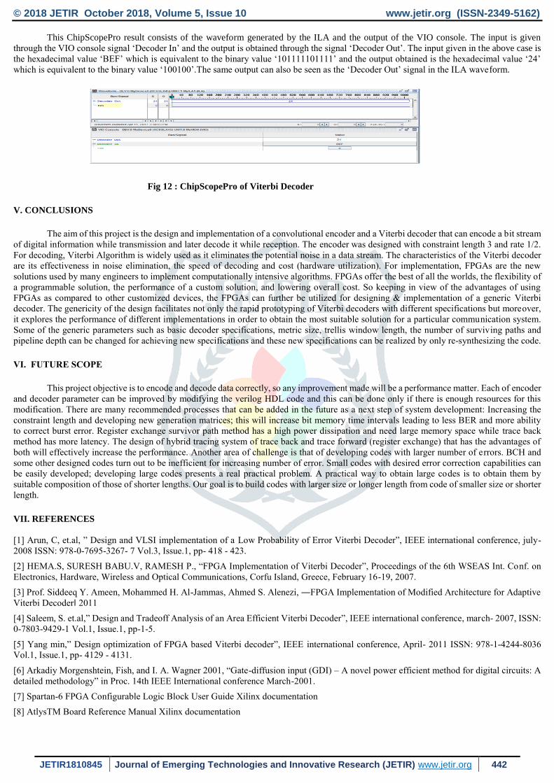
This ChipScopePro result consists of the waveform generated by the ILA and the output of the VIO console. The input is given
through the VIO console signal ‘Decoder In’ and the output is obtained through the signal ‘Decoder Out’. The input given in the above case is
the hexadecimal value ‘BEF’ which is equivalent to the binary value ‘101111101111’ and the output obtained is the hexadecimal value ‘24’
which is equivalent to the binary value ‘100100’.The same output can also be seen as the ‘Decoder Out’ signal in the ILA waveform.
Fig 12 : ChipScopePro of Viterbi Decoder
V. CONCLUSIONS
The aim of this project is the design and implementation of a convolutional encoder and a Viterbi decoder that can encode a bit stream
of digital information while transmission and later decode it while reception. The encoder was designed with constraint length 3 and rate 1/2.
For decoding, Viterbi Algorithm is widely used as it eliminates the potential noise in a data stream. The characteristics of the Viterbi decoder
are its effectiveness in noise elimination, the speed of decoding and cost (hardware utilization). For implementation, FPGAs are the new
solutions used by many engineers to implement computationally intensive algorithms. FPGAs offer the best of all the worlds, the flexibility of
a programmable solution, the performance of a custom solution, and lowering overall cost. So keeping in view of the advantages of using
FPGAs as compared to other customized devices, the FPGAs can further be utilized for designing & implementation of a generic Viterbi
decoder. The genericity of the design facilitates not only the rapid prototyping of Viterbi decoders with different specifications but moreover,
it explores the performance of different implementations in order to obtain the most suitable solution for a particular communication system.
Some of the generic parameters such as basic decoder specifications, metric size, trellis window length, the number of surviving paths and
pipeline depth can be changed for achieving new specifications and these new specifications can be realized by only re-synthesizing the code.
VI. FUTURE SCOPE
This project objective is to encode and decode data correctly, so any improvement made will be a performance matter. Each of encoder
and decoder parameter can be improved by modifying the verilog HDL code and this can be done only if there is enough resources for this
modification. There are many recommended processes that can be added in the future as a next step of system development: Increasing the
constraint length and developing new generation matrices; this will increase bit memory time intervals leading to less BER and more ability
to correct burst error. Register exchange survivor path method has a high power dissipation and need large memory space while trace back
method has more latency. The design of hybrid tracing system of trace back and trace forward (register exchange) that has the advantages of
both will effectively increase the performance. Another area of challenge is that of developing codes with larger number of errors. BCH and
some other designed codes turn out to be inefficient for increasing number of error. Small codes with desired error correction capabilities can
be easily developed; developing large codes presents a real practical problem. A practical way to obtain large codes is to obtain them by
suitable composition of those of shorter lengths. Our goal is to build codes with larger size or longer length from code of smaller size or shorter
length.
VII. REFERENCES
[1] Arun, C, et.al, ” Design and VLSI implementation of a Low Probability of Error Viterbi Decoder”, IEEE international conference, july-
2008 ISSN: 978-0-7695-3267- 7 Vol.3, Issue.1, pp- 418 - 423.
[2] HEMA.S, SURESH BABU.V, RAMESH P., “FPGA Implementation of Viterbi Decoder”, Proceedings of the 6th WSEAS Int. Conf. on
Electronics, Hardware, Wireless and Optical Communications, Corfu Island, Greece, February 16-19, 2007.
[3] Prof. Siddeeq Y. Ameen, Mohammed H. Al-Jammas, Ahmed S. Alenezi, ―FPGA Implementation of Modified Architecture for Adaptive
Viterbi Decoder‖ 2011
[4] Saleem, S. et.al,” Design and Tradeoff Analysis of an Area Efficient Viterbi Decoder”, IEEE international conference, march- 2007, ISSN:
0-7803-9429-1 Vol.1, Issue.1, pp-1-5.
[5] Yang min,” Design optimization of FPGA based Viterbi decoder”, IEEE international conference, April- 2011 ISSN: 978-1-4244-8036
Vol.1, Issue.1, pp- 4129 - 4131.
[6] Arkadiy Morgenshtein, Fish, and I. A. Wagner 2001, “Gate-diffusion input (GDI) – A novel power efficient method for digital circuits: A
detailed methodology” in Proc. 14th IEEE International conference March-2001.
[7] Spartan-6 FPGA Configurable Logic Block User Guide Xilinx documentation
[8] AtlysTM Board Reference Manual Xilinx documentation


![Unifying Performance Metric of Viterbi Decoders · 2.1 Rate-1/2 convolutional encoder with generator polynomials (G0=5, ... [3, 4, 5, 6, 7, 8]. ... of the Viterbi decoder come up](https://static.documents.pub/doc/80x56/5b62c25c7f8b9a54488de550/unifying-performance-metric-of-viterbi-decoders-21-rate-12-convolutional-encoder.jpg)


