NPN Transistors with Monolithic BiasResistor Network
This series of digital transistors is designed to replace a singledevice and its external resistor bias network. The Bias ResistorTransistor (BRT) contains a single transistor with a monolithic biasnetwork consisting of two resistors; a series base resistor and a base−emitter resistor. The BRT eliminates these individual components byintegrating them into a single device. The use of a BRT can reduceboth system cost and board space.
Features• Simplifies Circuit Design
• Reduces Board Space
• Reduces Component Count
• S and NSV Prefix for Automotive and Other Applications RequiringUnique Site and Control Change Requirements; AEC-Q101 Qualifiedand PPAP Capable
• These Devices are Pb−Free, Halogen Free/BFR Free and are RoHSCompliant
MAXIMUM RATINGS (TA = 25°C)
Rating Symbol Max Unit
Collector−Base Voltage VCBO 50 Vdc
Collector−Emitter Voltage VCEO 50 Vdc
Collector Current − Continuous IC 100 mAdc
Input Forward Voltage VIN(fwd) 40 Vdc
Input Reverse Voltage VIN(rev) 10 Vdc
Stresses exceeding those listed in the Maximum Ratings table may damage thedevice. If any of these limits are exceeded, device functionality should not beassumed, damage may occur and reliability may be affected.
PIN 3COLLECTOR
(OUTPUT)
PIN 2EMITTER
(GROUND)
PIN 1BASE
(INPUT)
R1
R2
See detailed ordering, marking, and shipping information inthe package dimensions section on page 2 of this data sheet.
ORDERING INFORMATION
SC−75CASE 463STYLE 1
MARKING DIAGRAMS
XXX = Specific Device CodeM = Date Code*� = Pb−Free Package
(Note: Microdot may be in either location)*Date Code orientation may vary depending up-
†For information on tape and reel specifications, including part orientation and tape sizes, please refer to our Tape and Reel PackagingSpecifications Brochure, BRD8011/D.
*S and NSV Prefix for Automotive and Other Applications Requiring Unique Site and Control Change Requirements; AEC−Q101 Qualified andPPAP Capable.
Figure 1. Derating Curve
AMBIENT TEMPERATURE (°C)
1251007550250−25−500
50
100
150
200
250
300
PD
, PO
WE
R D
ISS
IPA
TIO
N (
mW
)
150
(1) (2) (3) (4) (5)
(1) SC−75 and SC−70/SOT323; Minimum Pad(2) SC−59; Minimum Pad(3) SOT−23; Minimum Pad(4) SOT−1123; 100 mm2, 1 oz. copper trace(5) SOT−723; Minimum Pad
Thermal Resistance, (Note 1)Junction to Ambient (Note 2)
R�JA 600400
°C/W
Junction and Storage Temperature Range TJ, Tstg −55 to +150 °C
THERMAL CHARACTERISTICS (SOT−723) (DTC144EM3)
Total Device DissipationTA = 25°C (Note 1)
(Note 2)Derate above 25°C (Note 1)
(Note 2)
PD2606002.04.8
mW
mW/°C
Thermal Resistance, (Note 1)Junction to Ambient (Note 2)
R�JA 480205
°C/W
Junction and Storage Temperature Range TJ, Tstg −55 to +150 °C
1. FR−4 @ Minimum Pad.2. FR−4 @ 1.0 x 1.0 Inch Pad.3. FR−4 @ 100 mm2, 1 oz. copper traces, still air.4. FR−4 @ 500 mm2, 1 oz. copper traces, still air.
Thermal Resistance, (Note 3)Junction to Ambient (Note 4)
R�JA 493421
°C/W
Thermal Resistance, Junction to Lead(Note 3)
R�JL 193 °C/W
Junction and Storage Temperature Range TJ, Tstg −55 to +150 °C
1. FR−4 @ Minimum Pad.2. FR−4 @ 1.0 x 1.0 Inch Pad.3. FR−4 @ 100 mm2, 1 oz. copper traces, still air.4. FR−4 @ 500 mm2, 1 oz. copper traces, still air.
Product parametric performance is indicated in the Electrical Characteristics for the listed test conditions, unless otherwise noted. Productperformance may not be indicated by the Electrical Characteristics if operated under different conditions.5. Pulsed Condition: Pulse Width = 300 msec, Duty Cycle ≤ 2%.
XXX = Specific Device CodeM = Date Code� = Pb−Free Package
*This information is generic. Please refer todevice data sheet for actual part marking.Pb−Free indicator, “G” or microdot “ �”,may or may not be present.
GENERICMARKING DIAGRAM*
NOTES:1. DIMENSIONING AND TOLERANCING PER ASME Y14.5M, 1994.2. CONTROLLING DIMENSION: MILLIMETERS.3. MAXIMUM LEAD THICKNESS INCLUDES LEAD FINISH.
MINIMUM LEAD THICKNESS IS THE MINIMUM THICKNESS OFTHE BASE MATERIAL.
4. DIMENSIONS D AND E DO NOT INCLUDE MOLD FLASH,PROTRUSIONS, OR GATE BURRS.
ON Semiconductor and are trademarks of Semiconductor Components Industries, LLC dba ON Semiconductor or its subsidiaries in the United States and/or other countries.ON Semiconductor reserves the right to make changes without further notice to any products herein. ON Semiconductor makes no warranty, representation or guarantee regardingthe suitability of its products for any particular purpose, nor does ON Semiconductor assume any liability arising out of the application or use of any product or circuit, and specificallydisclaims any and all liability, including without limitation special, consequential or incidental damages. ON Semiconductor does not convey any license under its patent rights nor therights of others.
98ASB42226BDOCUMENT NUMBER:
DESCRIPTION:
Electronic versions are uncontrolled except when accessed directly from the Document Repository.Printed versions are uncontrolled except when stamped “CONTROLLED COPY” in red.
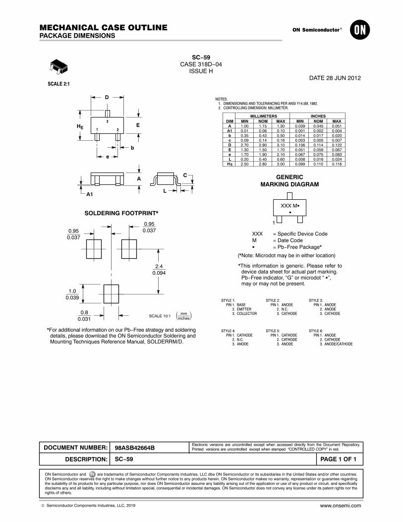
NOTES:1. DIMENSIONING AND TOLERANCING PER ANSI Y14.5M, 1982.2. CONTROLLING DIMENSION: MILLIMETER.
2.40.094
0.950.037
0.950.037
1.00.039
0.80.031
� mminches
�SCALE 10:1
XXX M�
�
XXX = Specific Device CodeM = Date Code� = Pb−Free Package*
GENERICMARKING DIAGRAM
*This information is generic. Please refer todevice data sheet for actual part marking.Pb−Free indicator, “G” or microdot “ �”,may or may not be present.
1
*For additional information on our Pb−Free strategy and solderingdetails, please download the ON Semiconductor Soldering andMounting Techniques Reference Manual, SOLDERRM/D.
ON Semiconductor and are trademarks of Semiconductor Components Industries, LLC dba ON Semiconductor or its subsidiaries in the United States and/or other countries.ON Semiconductor reserves the right to make changes without further notice to any products herein. ON Semiconductor makes no warranty, representation or guarantee regardingthe suitability of its products for any particular purpose, nor does ON Semiconductor assume any liability arising out of the application or use of any product or circuit, and specificallydisclaims any and all liability, including without limitation special, consequential or incidental damages. ON Semiconductor does not convey any license under its patent rights nor therights of others.
98ASB42664BDOCUMENT NUMBER:
DESCRIPTION:
Electronic versions are uncontrolled except when accessed directly from the Document Repository.Printed versions are uncontrolled except when stamped “CONTROLLED COPY” in red.
XX = Specific Device CodeM = Date Code� = Pb−Free Package
GENERICMARKING DIAGRAM
1
STYLE 11:PIN 1. CATHODE
2. CATHODE3. CATHODE
*This information is generic. Please refer todevice data sheet for actual part marking.Pb−Free indicator, “G” or microdot “�”, mayor may not be present. Some products maynot follow the Generic Marking.
MECHANICAL CASE OUTLINE
PACKAGE DIMENSIONS
98ASB42819BDOCUMENT NUMBER:
DESCRIPTION:
Electronic versions are uncontrolled except when accessed directly from the Document Repository.Printed versions are uncontrolled except when stamped “CONTROLLED COPY” in red.
PAGE 1 OF 1SC−70 (SOT−323)
onsemi and are trademarks of Semiconductor Components Industries, LLC dba onsemi or its subsidiaries in the United States and/or other countries. onsemi reservesthe right to make changes without further notice to any products herein. onsemi makes no warranty, representation or guarantee regarding the suitability of its products for any particularpurpose, nor does onsemi assume any liability arising out of the application or use of any product or circuit, and specifically disclaims any and all liability, including without limitationspecial, consequential or incidental damages. onsemi does not convey any license under its patent rights nor the rights of others.
*This information is generic. Please refer todevice data sheet for actual part marking.Pb−Free indicator, “G” or microdot “ �”,may or may not be present.
GENERICMARKING DIAGRAM*
HE
L 0.10 0.15 0.201.50 1.60 1.70
0.004 0.006 0.0080.060 0.063 0.067
0.70 0.80 0.90 0.027 0.031 0.035
0.7870.031
0.5080.020 1.000
0.039
� mminches
�SCALE 10:1
0.3560.014
*For additional information on our Pb−Free strategy and solderingdetails, please download the ON Semiconductor Soldering andMounting Techniques Reference Manual, SOLDERRM/D.
SOLDERING FOOTPRINT*
1 2
3
1.8030.071
MECHANICAL CASE OUTLINE
PACKAGE DIMENSIONS
ON Semiconductor and are trademarks of Semiconductor Components Industries, LLC dba ON Semiconductor or its subsidiaries in the United States and/or other countries.ON Semiconductor reserves the right to make changes without further notice to any products herein. ON Semiconductor makes no warranty, representation or guarantee regardingthe suitability of its products for any particular purpose, nor does ON Semiconductor assume any liability arising out of the application or use of any product or circuit, and specificallydisclaims any and all liability, including without limitation special, consequential or incidental damages. ON Semiconductor does not convey any license under its patent rights nor therights of others.
98ASB15184CDOCUMENT NUMBER:
DESCRIPTION:
Electronic versions are uncontrolled except when accessed directly from the Document Repository.Printed versions are uncontrolled except when stamped “CONTROLLED COPY” in red.
1. DIMENSIONING AND TOLERANCING PER ASMEY14.5M, 1994.
2. CONTROLLING DIMENSION: MILLIMETERS.3. MAXIMUM LEAD THICKNESS INCLUDES LEAD
FINISH. MINIMUM LEAD THICKNESS IS THEMINIMUM THICKNESS OF BASE MATERIAL.
4. DIMENSIONS D AND E DO NOT INCLUDE MOLDFLASH, PROTRUSIONS, OR GATE BURRS.
GENERICMARKING DIAGRAM*
X = Specific Device CodeM = Date Code
*This information is generic. Please referto device data sheet for actual partmarking.Pb−Free indicator, “G” or microdot “ �”,may or may not be present.
DIM MIN MAXMILLIMETERS
A 0.34 0.40b 0.15 0.28
c 0.07 0.17D 0.75 0.85E 0.55 0.65
0.95 1.05L 0.185 REF
HE
D
E
c
A
−Y−
−X−
HE
*For additional information on our Pb−Free strategy and solderingdetails, please download the ON Semiconductor Soldering andMounting Techniques Reference Manual, SOLDERRM/D.
SOLDERING FOOTPRINT*
X M
e
b1 0.10 0.20
STYLE 1:PIN 1. BASE
2. EMITTER 3. COLLECTOR
STYLE 2:PIN 1. ANODE
2. N/C 3. CATHODE
STYLE 3:PIN 1. ANODE
2. ANODE 3. CATHODE
STYLE 4:PIN 1. CATHODE
2. CATHODE 3. ANODE
STYLE 5:PIN 1. GATE
2. SOURCE 3. DRAIN
1
2
3
0.35 0.40
TOP VIEW
SIDE VIEW
3X
BOTTOM VIEW
L2
L3X
DIMENSIONS: MILLIMETERS
1.20
2X
0.263X 0.34
PACKAGEOUTLINE
b
2X b1
e0.08 X Y
L2 0.05 0.15
0.200.38
1
MECHANICAL CASE OUTLINE
PACKAGE DIMENSIONS
ON Semiconductor and are trademarks of Semiconductor Components Industries, LLC dba ON Semiconductor or its subsidiaries in the United States and/or other countries.ON Semiconductor reserves the right to make changes without further notice to any products herein. ON Semiconductor makes no warranty, representation or guarantee regardingthe suitability of its products for any particular purpose, nor does ON Semiconductor assume any liability arising out of the application or use of any product or circuit, and specificallydisclaims any and all liability, including without limitation special, consequential or incidental damages. ON Semiconductor does not convey any license under its patent rights nor therights of others.
98AON23134DDOCUMENT NUMBER:
DESCRIPTION:
Electronic versions are uncontrolled except when accessed directly from the Document Repository.Printed versions are uncontrolled except when stamped “CONTROLLED COPY” in red.
Y14.5M, 1994.2. CONTROLLING DIMENSION: MILLIMETERS.3. MAXIMUM LEAD THICKNESS INCLUDES LEAD
FINISH. MINIMUM LEAD THICKNESS IS THE MINIMUMTHICKNESS OF BASE MATERIAL.
4. DIMENSIONS D AND E DO NOT INCLUDE MOLDFLASH, PROTRUSIONS OR GATE BURRS.
Db1
E
be
A
L
C
H
−Y−
−X−
X0.08 Y2X
E
1 2
3
XX = Specific Device CodeM = Date Code
GENERICMARKING DIAGRAM*
SCALE 4:1
XX MSTYLE 1:
PIN 1. BASE 2. EMITTER 3. COLLECTOR
STYLE 2:PIN 1. ANODE
2. N/C 3. CATHODE
STYLE 3:PIN 1. ANODE
2. ANODE 3. CATHODE
STYLE 4:PIN 1. CATHODE
2. CATHODE 3. ANODE
1
*This information is generic. Please referto device data sheet for actual partmarking. Pb−Free indicator, “G”, mayor not be present.
*For additional information on our Pb−Free strategy and solderingdetails, please download the ON Semiconductor Soldering andMounting Techniques Reference Manual, SOLDERRM/D.
SOLDERING FOOTPRINT*
STYLE 5:PIN 1. GATE
2. SOURCE 3. DRAIN
L2 0.15 0.20 0.250.29 REF
3X
L23X
1
2X
TOP VIEW
BOTTOM VIEW
SIDE VIEW
RECOMMENDED
DIMENSIONS: MILLIMETERS
0.40
1.50
2X
PACKAGEOUTLINE
0.272X
0.523X 0.36
MECHANICAL CASE OUTLINE
PACKAGE DIMENSIONS
ON Semiconductor and are trademarks of Semiconductor Components Industries, LLC dba ON Semiconductor or its subsidiaries in the United States and/or other countries.ON Semiconductor reserves the right to make changes without further notice to any products herein. ON Semiconductor makes no warranty, representation or guarantee regardingthe suitability of its products for any particular purpose, nor does ON Semiconductor assume any liability arising out of the application or use of any product or circuit, and specificallydisclaims any and all liability, including without limitation special, consequential or incidental damages. ON Semiconductor does not convey any license under its patent rights nor therights of others.
98AON12989DDOCUMENT NUMBER:
DESCRIPTION:
Electronic versions are uncontrolled except when accessed directly from the Document Repository.Printed versions are uncontrolled except when stamped “CONTROLLED COPY” in red.
onsemi, , and other names, marks, and brands are registered and/or common law trademarks of Semiconductor Components Industries, LLC dba “onsemi” or its affiliatesand/or subsidiaries in the United States and/or other countries. onsemi owns the rights to a number of patents, trademarks, copyrights, trade secrets, and other intellectual property.A listing of onsemi’s product/patent coverage may be accessed at www.onsemi.com/site/pdf/Patent−Marking.pdf. onsemi reserves the right to make changes at any time to anyproducts or information herein, without notice. The information herein is provided “as−is” and onsemi makes no warranty, representation or guarantee regarding the accuracy of theinformation, product features, availability, functionality, or suitability of its products for any particular purpose, nor does onsemi assume any liability arising out of the application or useof any product or circuit, and specifically disclaims any and all liability, including without limitation special, consequential or incidental damages. Buyer is responsible for its productsand applications using onsemi products, including compliance with all laws, regulations and safety requirements or standards, regardless of any support or applications informationprovided by onsemi. “Typical” parameters which may be provided in onsemi data sheets and/or specifications can and do vary in different applications and actual performance mayvary over time. All operating parameters, including “Typicals” must be validated for each customer application by customer’s technical experts. onsemi does not convey any licenseunder any of its intellectual property rights nor the rights of others. onsemi products are not designed, intended, or authorized for use as a critical component in life support systemsor any FDA Class 3 medical devices or medical devices with a same or similar classification in a foreign jurisdiction or any devices intended for implantation in the human body. ShouldBuyer purchase or use onsemi products for any such unintended or unauthorized application, Buyer shall indemnify and hold onsemi and its officers, employees, subsidiaries, affiliates,and distributors harmless against all claims, costs, damages, and expenses, and reasonable attorney fees arising out of, directly or indirectly, any claim of personal injury or deathassociated with such unintended or unauthorized use, even if such claim alleges that onsemi was negligent regarding the design or manufacture of the part. onsemi is an EqualOpportunity/Affirmative Action Employer. This literature is subject to all applicable copyright laws and is not for resale in any manner.


![[A4] XIAOMEI_Guangzhou BRT and New BRT in China - Ed](https://static.documents.pub/doc/80x56/577ce47b1a28abf1038e73a0/a4-xiaomeiguangzhou-brt-and-new-brt-in-china-ed.jpg)


