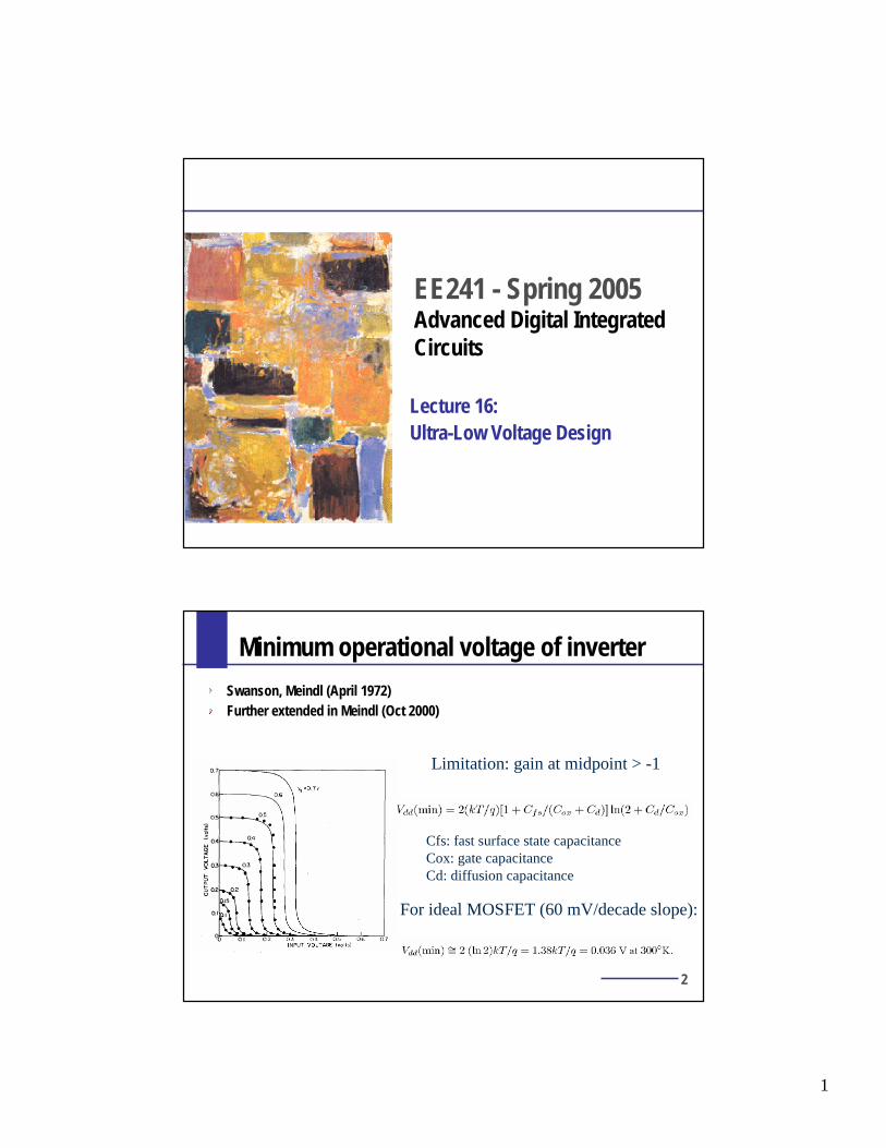
1 EE241 - Spring 2005 Advanced Digital Integrated Circuits Lecture 16: Ultra-Low Voltage Design 2 Minimum operational voltage of inverter Swanson, Meindl (April 1972) Further extended in Meindl (Oct 2000) Limitation: gain at midpoint > -1 Cfs: fast surface state capacitance Cox: gate capacitance Cd: diffusion capacitance For ideal MOSFET (60 mV/decade slope):
Transcript
1
EE241 - Spring 2005Advanced Digital Integrated Circuits
Lecture 16:Ultra-Low Voltage Design
2
Minimum operational voltage of inverter
Swanson, Meindl (April 1972)Further extended in Meindl (Oct 2000)
Limitation: gain at midpoint > -1
Cfs: fast surface state capacitanceCox: gate capacitanceCd: diffusion capacitance
For ideal MOSFET (60 mV/decade slope):
2
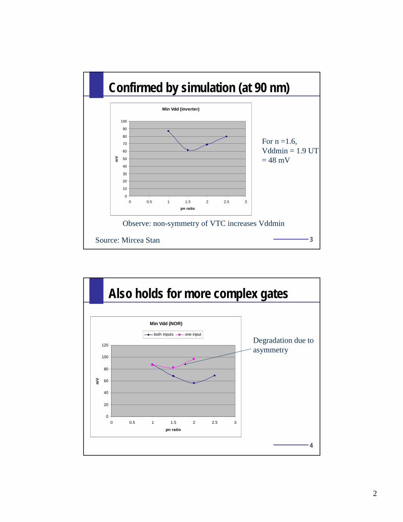
3
Confirmed by simulation (at 90 nm)Min Vdd (inverter)
0
10
20
30
40
50
60
70
80
90
100
0 0.5 1 1.5 2 2.5 3
pn ratio
mV
Source: Mircea Stan
Observe: non-symmetry of VTC increases Vddmin
For n =1.6,Vddmin = 1.9 UT= 48 mV
4
Also holds for more complex gates
Min Vdd (NOR)
0
20
40
60
80
100
120
0 0.5 1 1.5 2 2.5 3
pn ratio
mV
both inputs one input
Degradation due toasymmetry
3
5
Minimum energy per operation
Predicted by von Neumann: kTln(2)
Based on previous result – moving one electron over Vddmin:
Emin = QVDD/2 = q 2(ln2)kT/2q = kTln(2)
Would be approximately three times larger for CMOS inverter withPMOS twice the size of NMOS
At room temperature (300K): Emin = 0.29 10-20 J
Minimum sized CMOS inverter at 90 nm operating at 1VE = CVdd2 = 0.8 10-15 J, or 5 orders of magnitude larger!
6
Why Worry about Power?
Total Energy of Milky Way Galaxy: 1059 J
Minimum switching energy for digital gate (1 electron@100 mV): 1.6 10-20 J (limited by thermal noise)
Upper bound on number of digital operations: 6 1078
Operations/year performed by 1 billion 100 MOPS computers: 3 1024
Energy consumed in 180 years assuming a doubling of computational requirements every year.
4
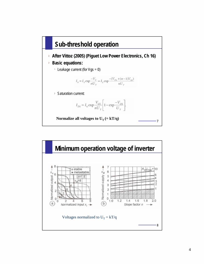
7
Sub-threshold operation
After Vittoz (2005) (Piguet Low Power Electronics, Ch 16)
Basic equations:Leakage current (for Vgs = 0)
Saturation current:
Normalize all voltages to UT (= kT/q)
8
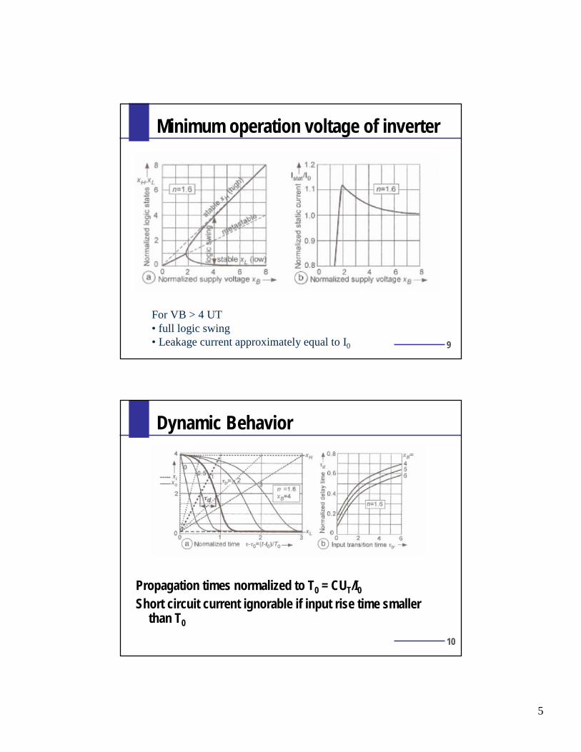
Minimum operation voltage of inverter
Voltages normalized to UT = kT/q
5
9
Minimum operation voltage of inverter
For VB > 4 UT • full logic swing• Leakage current approximately equal to I0
10
Dynamic Behavior
Propagation times normalized to T0 = CUT/I0Short circuit current ignorable if input rise time smaller
than T0
6
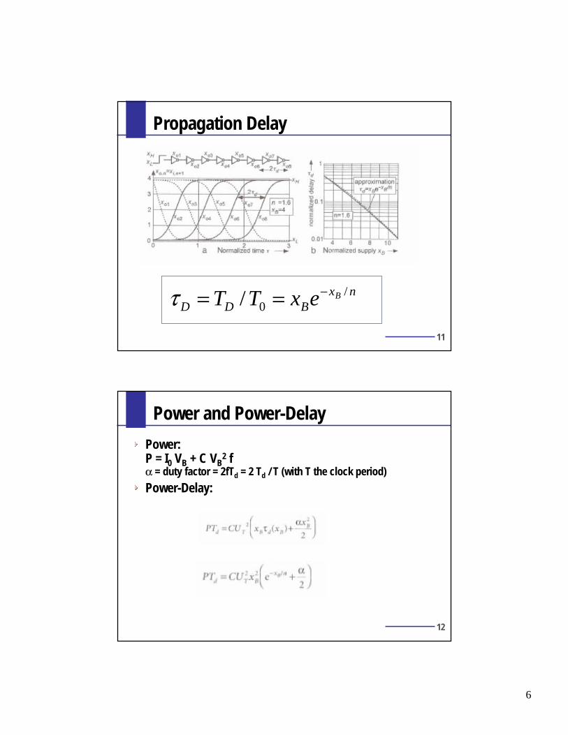
11
Propagation Delay
nxBDD
BexTT /0/ −==τ
12
Power and Power-Delay
Power:P = I0 VB + C VB
2 fα = duty factor = 2fTd = 2 Td / T (with T the clock period)
Power-Delay:
7
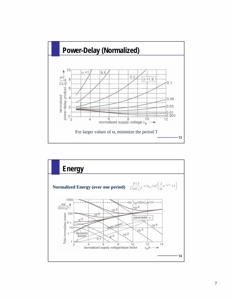
13
Power-Delay (Normalized)
For larger values of α, minimize the period T
14
Energy
Normalized Energy (over one period)
8
15
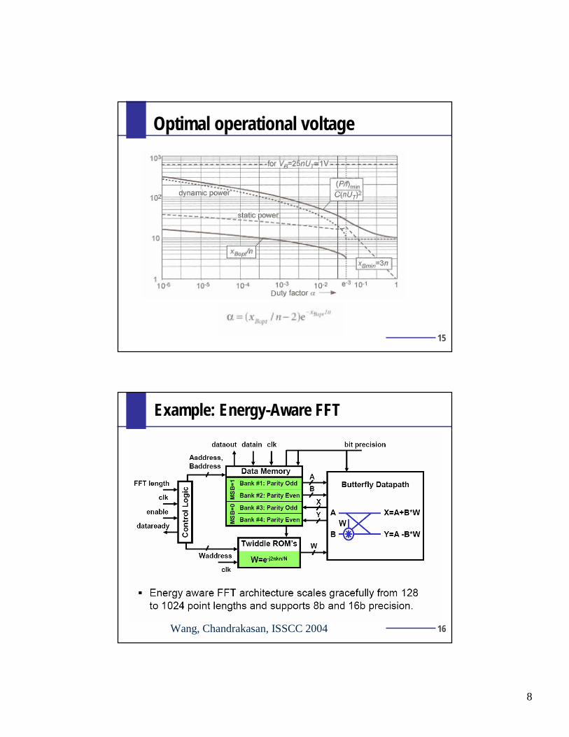
Optimal operational voltage
16
Example: Energy-Aware FFT
Wang, Chandrakasan, ISSCC 2004
9
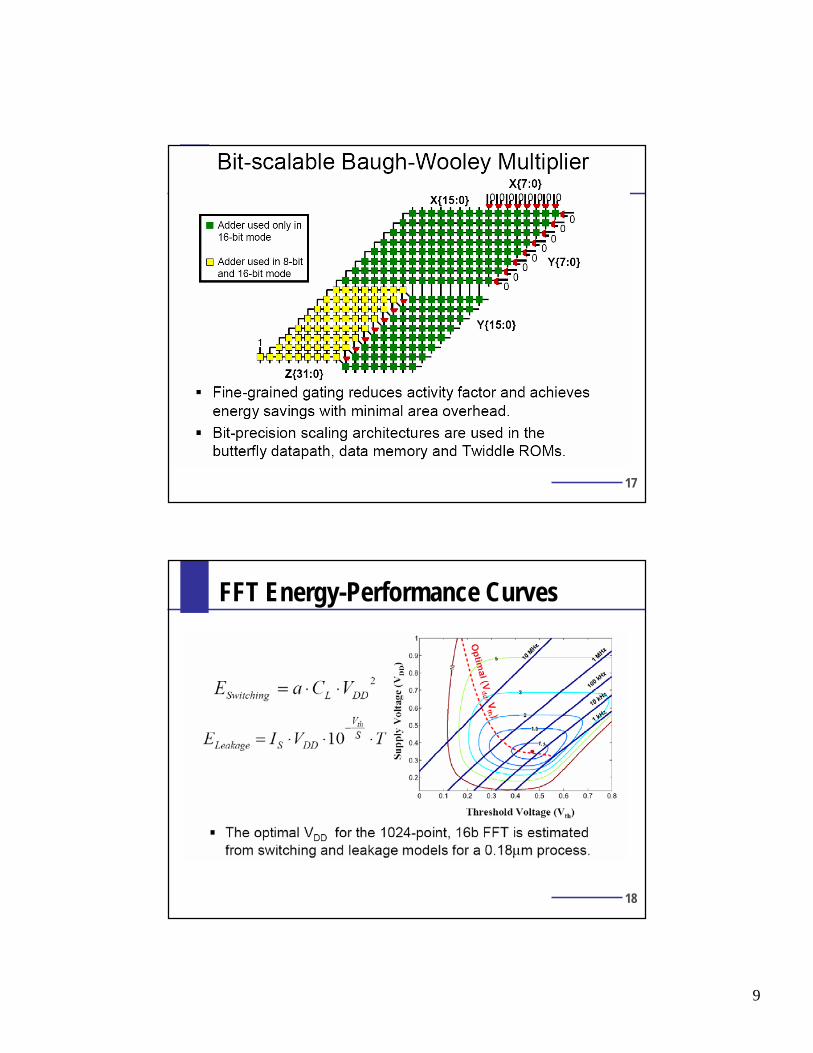
17
18
FFT Energy-Performance Curves
10
19
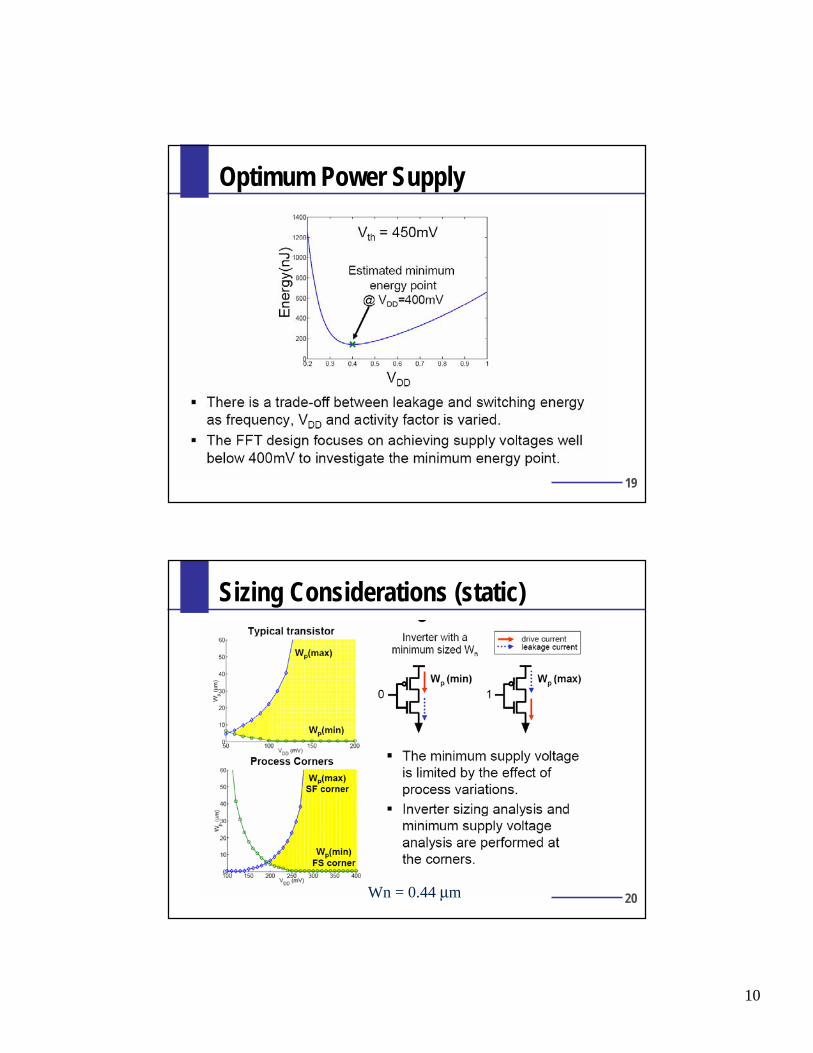
Optimum Power Supply
20
Sizing Considerations (static)
Wn = 0.44 µm
11
21
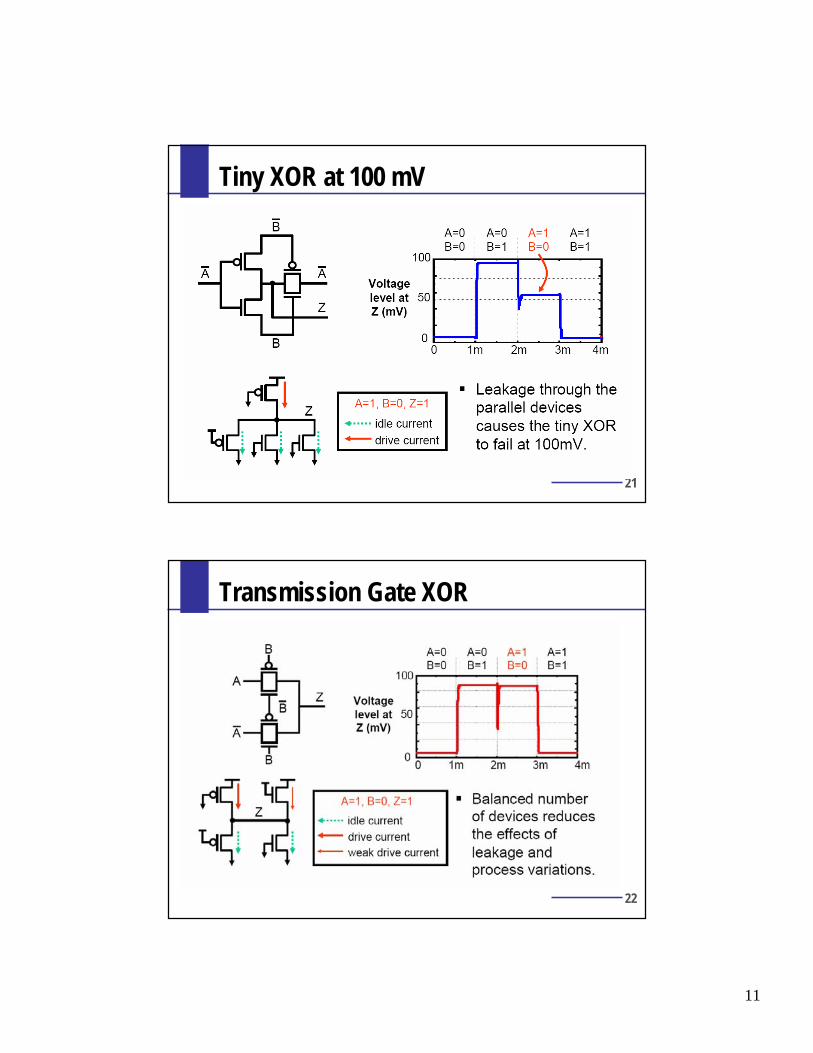
Tiny XOR at 100 mV
22
Transmission Gate XOR
12
23
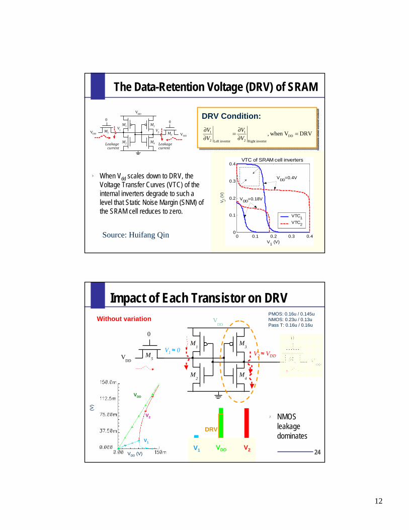
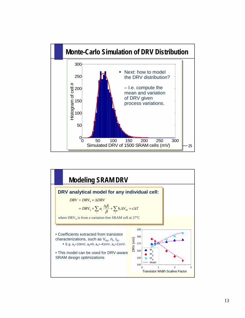
The Data-Retention Voltage (DRV) of SRAM
DRVV when , DD
inverterRight 2
1
inverterLeft 2
1 =∂∂=
∂∂
V
V
V
V
VDD
V1
M4
M3
M6M5
M2
M1
Leakagecurrent
V2
Leakagecurrent
VDDVDD
0 0
0 0.1 0.2 0.3 0.40
0.1
0.2
0.3
0.4
V1 (V)
2
VTC1VTC2
VDD=0.18V
VDD=0.4V
VTC of SRAM cell inverters
V2
(V)
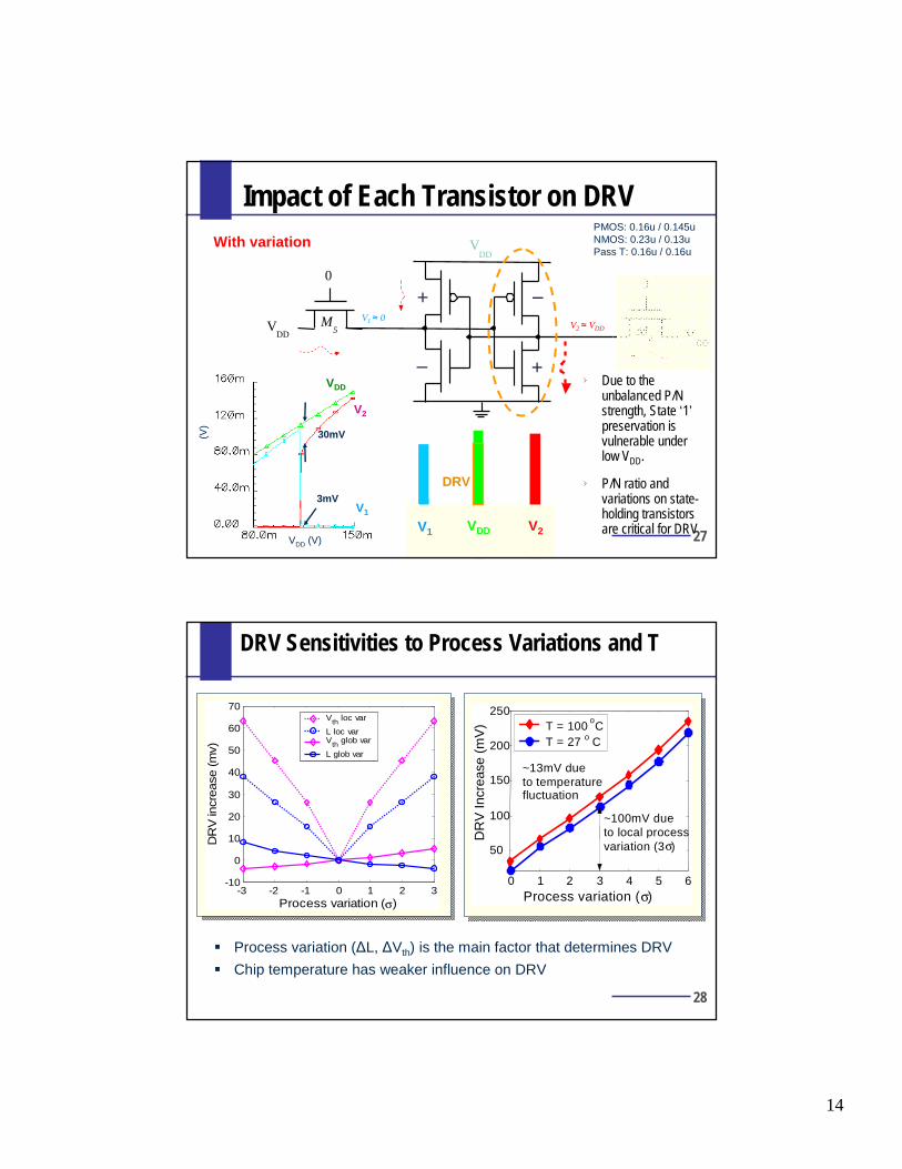
When Vdd scales down to DRV, the Voltage Transfer Curves (VTC) of the internal inverters degrade to such a level that Static Noise Margin (SNM) of the SRAM cell reduces to zero.
Due to the unbalanced P/N strength, State ‘1’preservation is vulnerable under low VDD.
P/N ratio and variations on state-holding transistors are critical for DRV
+
+–
–
DRV
28
DRV Sensitivities to Process Variations and T
0 1 2 3 4 5 6
50
100
150
200
250
Process variation ( σ )
DR
V In
crea
se (
mV
) T = 100 o C T = 27 o C
~100mV due to local process variation (3 σ )
~13mV due to temperature fluctuation
Process variation (∆L, ∆Vth) is the main factor that determines DRV
Chip temperature has weaker influence on DRV
-3 -2 -1 0 1 2 3-10
0
10
20
30
40
50
60
70
Process variation (σ)
DR
V in
crease
(m
v)
Vth loc var
L loc varVth glob var
L glob var
15
29
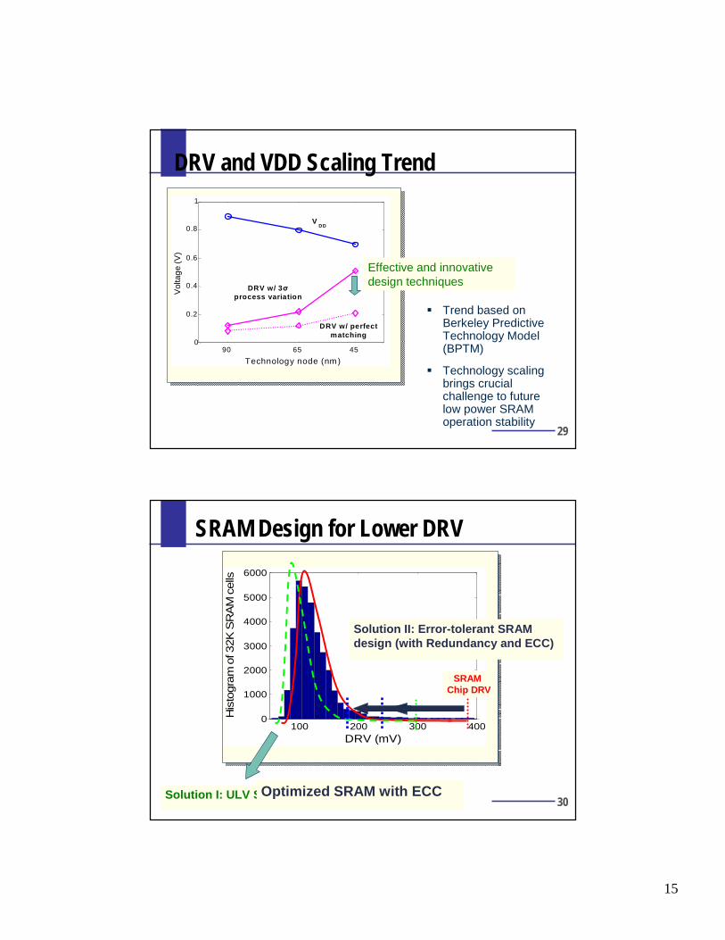
DRV and VDD Scaling Trend
Trend based on Berkeley Predictive Technology Model (BPTM)
Technology scaling brings crucial challenge to future low power SRAM operation stability
45 65 90 0
0.2
0.4
0.6
0.8
1
Technology node (nm)
Vol
tage
(V
)
DRV w/ perfect matching
DRV w/ 3σ process variation
V DD
Effective and innovative design techniques
30
SRAM Design for Lower DRV
100 200 300 4000
1000
2000
3000
4000
5000
6000
DRV (mV)
His
togr
am
of 3
2K S
RA
M c
ells
Solution I: ULV SRAM design optimization
SRAM Chip DRV
Solution II: Error-tolerant SRAM design (with Redundancy and ECC)
Optimized SRAM with ECC
16
31
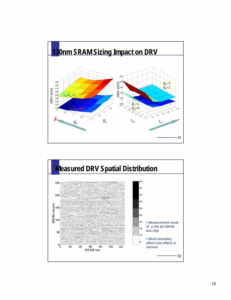
130nm SRAM Sizing Impact on DRV
1
1.5
2
2.5
3
11.5
22.5
3110
120
130
140
150
160
170
180
190
βnβp
DR
V (
mV
)
11.2
1.41.6
1.82
2.2
11.2
1.41.6
1.82
2.2100
120
140
160
180
200
LnLp
DR
V (
mV
)
Ln=Lp=2.2
Ln=Lp=1
βn=3βp=1
βn=1βp=3
32
Measured DRV Spatial Distribution
• Measurement result of a 32k bit SRAM test chip
• Block boundary effect (row effect) is obvious.
17
33
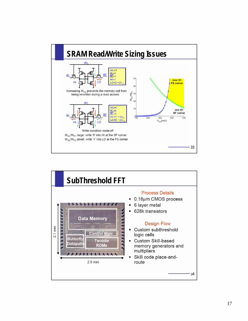
SRAM Read/Write Sizing Issues
34
SubThreshold FFT
18
35
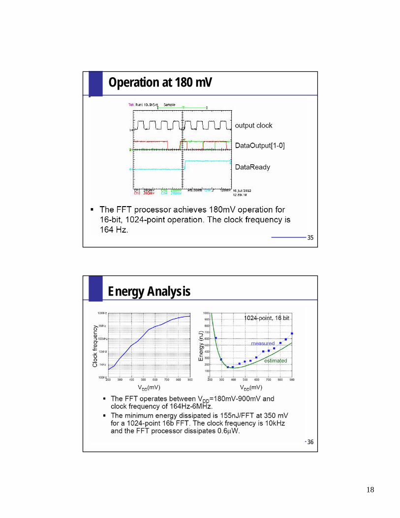
Operation at 180 mV
36
Energy Analysis
19
37
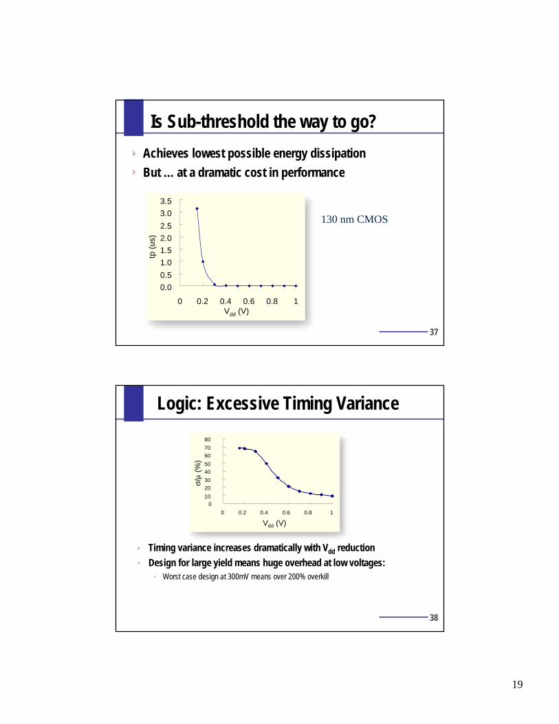
Is Sub-threshold the way to go?
Achieves lowest possible energy dissipation
But … at a dramatic cost in performance
0.0
0.5
1.0
1.5
2.0
2.5
3.0
3.5
0 0.2 0.4 0.6 0.8 1Vdd (V)
tp(u
s)
130 nm CMOS
38
Logic: Excessive Timing Variance
010
2030
4050
6070
80
0 0.2 0.4 0.6 0.8 1
Vdd (V)
σ/µ
(%)
Timing variance increases dramatically with Vdd reduction
Design for large yield means huge overhead at low voltages:Worst case design at 300mV means over 200% overkill
20
39
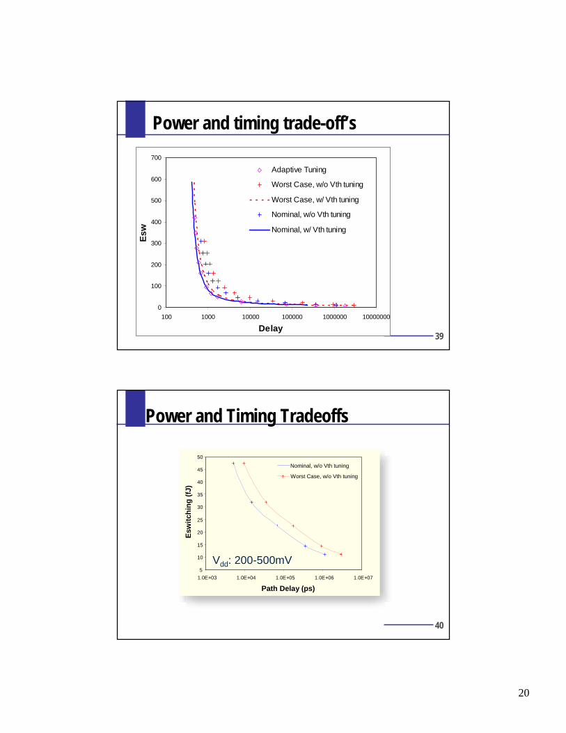
Power and timing trade-off’s
0
100
200
300
400
500
600
700
100 1000 10000 100000 1000000 10000000
Delay
Esw
Adaptive Tuning
Worst Case, w/o Vth tuning
Worst Case, w/ Vth tuning
Nominal, w/o Vth tuning
Nominal, w/ Vth tuning
40
Power and Timing Tradeoffs
5
10
15
20
25
30
35
40
45
50
1.0E+03 1.0E+04 1.0E+05 1.0E+06 1.0E+07
Path Delay (ps)
Esw
itch
ing
(fJ)
Worst Case, w/o Vth tuning
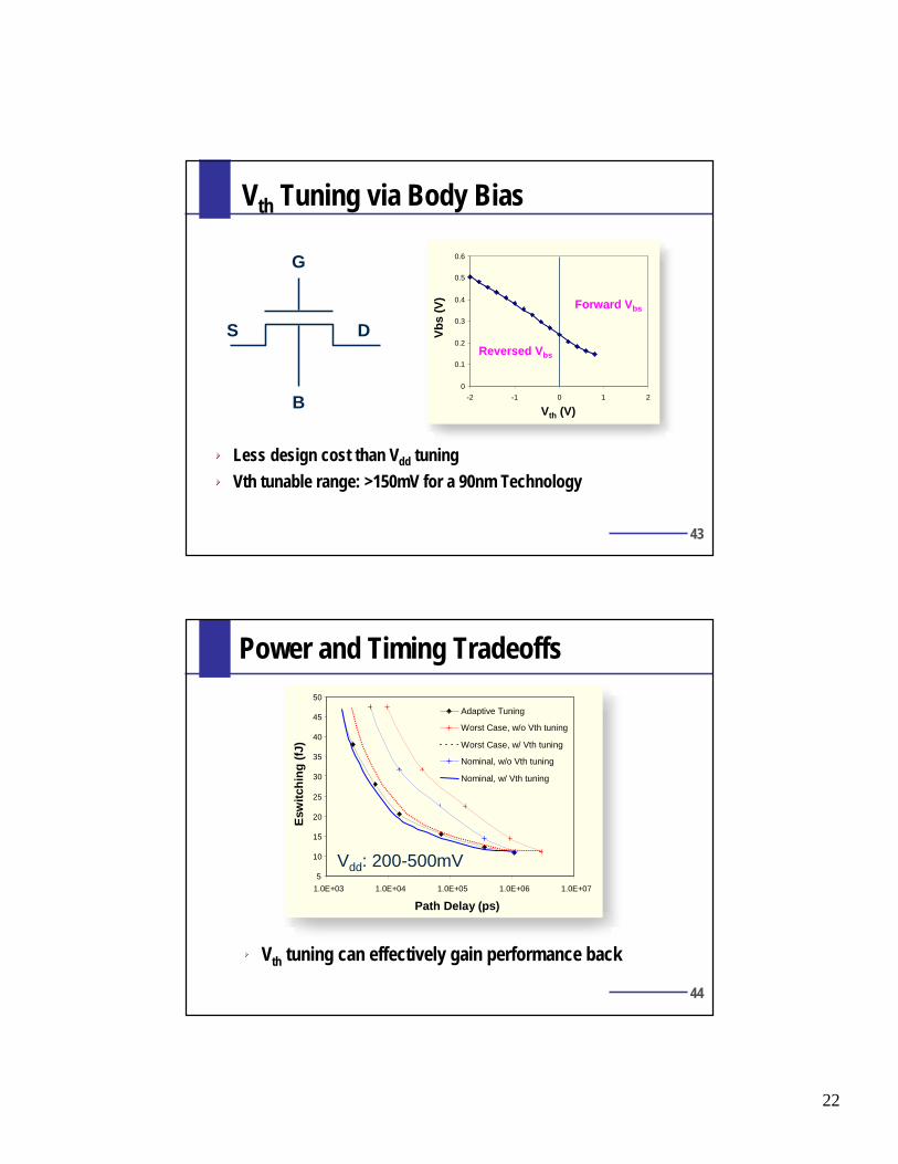
Nominal, w/o Vth tuning
Vdd: 200-500mV
21
41
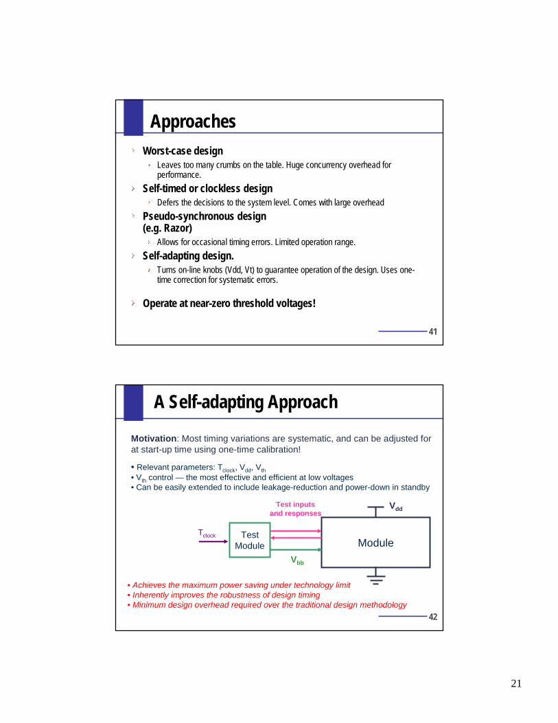
ApproachesWorst-case design
Leaves too many crumbs on the table. Huge concurrency overhead for performance.
Self-timed or clockless designDefers the decisions to the system level. Comes with large overhead
Pseudo-synchronous design (e.g. Razor)
Allows for occasional timing errors. Limited operation range.
Self-adapting design.Turns on-line knobs (Vdd, Vt) to guarantee operation of the design. Uses one-time correction for systematic errors.
Operate at near-zero threshold voltages!
42
A Self-adapting Approach
Module
Motivation: Most timing variations are systematic, and can be adjusted forat start-up time using one-time calibration!
• Relevant parameters: Tclock, Vdd, Vth• Vth control — the most effective and efficient at low voltages• Can be easily extended to include leakage-reduction and power-down in standby
TestModule
Vdd
Vbb
Test inputsand responses
Tclock
• Achieves the maximum power saving under technology limit• Inherently improves the robustness of design timing• Minimum design overhead required over the traditional design methodology