140
FAU Studien Materialwissenschaft und Werkstofftechnik 4 Michael Salinas Interface Engineering with Self-assembled Monolayers for Organic Electronics

FAU Studien Materialwissenschaft und Werkstofftechnik 4
UNIVERSITY P R E S S
Michael Salinas
Interface Engineering with Self-assembled Monolayersfor Organic Electronics
Mic
hael
Sal
inas
In
terfa
ce E
ngin
eerin
g w
ith S
elf-
asse
mbl
ed M
onol
ayer
s fo
r O
rgan
ic E
lect
roni
cs
FAU
UN
IVE
RS
ITY
PR
ES
S 2
014
ISBN 978-3-944057-21-7


Interface Engineering with Self-assembled Monolayers for Organic Electronics
Modifikation von Grenzflächen mit selbst-organisierten
Monolagen in der organischen Elektronik
Der Technischen Fakultät
der Friedrich-Alexander-Universität
Erlangen-Nürnberg
zur Erlangung des Doktorgrades Dr.-Ing.
vorgelegt von
Michael Walter Salinas Batallas
aus Stuttgart

Als Dissertation genehmigt
von der Technischen Fakultät der
Friedrich-Alexander-Universität Erlangen-Nürnberg
Tag der mündlichen Prüfung: 25.03.2014
Vorsitzende des Promotionsorgans:
Prof. Dr.-Ing. habil. Marion Merklein
Gutachter:
Prof. Dr. Marcus Halik Prof. Dr. Christoph J. Brabec

Abstract
The work presented in this thesis focuses on the impact of densely packed dipolar self-assembled monolayers (SAMs) on the electrical characteristics of organic electronic devices. The main achievement was in deducing the relationship between the dipolar character of self-assembled monolayers applied as part of a hybrid dielectric and the switching behavior of organic thin-film transistors (OTFTs). Further important aspects of this work are the general understanding of material properties that contribute to the electrical device characteristics and the estimation of the magnitude of their contribution to specific electrical device parameters. The approach presented in this thesis combines experimental methods applied for the determination of different SAM properties (relative permittivity, layer thickness and packing density) and computational methods applied for the calculation of SAM dipole moments and work functions of organic semiconductors. A model that correlates the threshold voltage shift with the electrostatic potential of a SAM is proposed. The quantitative correlation is supported by the good agreement of calculated values with experimentally determined parameters of the transistors. The change of the charge carrier density in the semiconductor is explained by charge rearrangements induced by the dipole moment of the SAM. Photoconductive and photovoltaic effects in OTFTs were investigated by using SAM molecules with an electro-optical functionality. This approach provided the possibility to tune the photoinduced charge transfer at the interface of semiconductor and SAM. Finally, electron extraction layers of organic solar cells (OSCs) were modified with C60 functionalized SAM molecules, improving the charge transfer to the active material. The modification led to increased fill factors and short circuit current densities of the OSCs.


Kurzfassung
Die vorliegende Arbeit widmet sich dem Einsatz von selbst-organisierten Monolagen (SAMs) in der organischen Elektronik und dem damit verbundenen Einfluss der SAMs auf die Eigenschaften der elektronischen Bauteile. Schwerpunkt der Arbeit ist der Einsatz von SAMs als Be-standteil von hybriden Dielektrika in organischen Dünnfilmtransistoren (OTFTs). Der Zusammenhang zwischen dem Dipol-Charakter der SAMs und dem Schaltverhalten der OTFTs wird hierbei eingehend untersucht. Ein weiteres Ziel dieser Arbeit ist die Entwicklung eines grundlegenden Verständnisses für die Zusammenhänge zwischen Material- und Bauteil-eigenschaften. Hierbei soll auch eine Abschätzung ermöglicht werden, wie stark sich die jeweilige Materialeigenschaft auf einen spezifischen Bauteilparameter auswirkt. Im Rahmen dieser Studie wurden unter anderem die relative Permittivität, die Dicke und die Packungsdichte der eingesetzten Schichten experimentell bestimmt sowie Dipolmomente und Austrittsarbeiten der Materialien berechnet. Auf Grundlage der Ergebnisse dieser Studie wurde ein Modell abgeleitet, das den Zusammenhang zwischen der Transistor-Schwellspannung und dem elektrostatischen Potential von SAMs erklärt. Hierbei induziert das Dipolmoment der SAM eine Umordnung der Ladungsträger an der Grenzfläche, was auch eine Änderung der Ladungsträgerdichte im Halb-leiter zur Folge hat. Die experimentell ermittelten Transistor-Parameter und die anhand des Modells berechneten Werte für das elektrostatische Potential zeigen eine gute Übereinstimmung. Das Auftreten von Photoleitfähigkeit und photovoltaischem Effekt in OTFTs wurde mithilfe des Einsatzes von photoaktiven SAM-Molekülen untersucht. Dieses Konzept bietet die Möglichkeit, den photoinduzierten Ladungstransfer zwischen SAM und Halbleiter in einem gewissen Um-fang zu steuern. Schließlich wurden Elektronen-Transportschichten in organischen Solarzellen mit C60 funktionalisierten SAMs modifiziert. Der dadurch optimierte Ladungstransfer an der Grenzfläche zum aktiven Material führte zu einer Verbesserung des Füllfaktors und der Kurzschluss-stromdichte.


List of contents i
List of contents
1. Introduction .............................................................................................. 1
2. Theoretical background ....................................................................... 3 2.1 Self-assembled monolayers ................................................................................ 3
2.1.1 Self-assembled monolayer systems ................................................................. 3 2.1.2 Formation and growth of SAMs ......................................................................... 4 2.1.3 Characterization of SAMs ...................................................................................... 7 2.1.4 Electronic properties of SAMs ............................................................................ 9
2.2 Optical excitation of organic materials ........................................................ 13 2.3 Electronic devices ............................................................................................... 14
2.3.1 Capacitor .................................................................................................................... 14 2.3.2 Organic thin-film transistor ............................................................................... 15 2.3.3 Concept of threshold voltage in OTFTs and the role of interfacial
dipoles ......................................................................................................................... 21 2.3.4 Organic phototransistor ...................................................................................... 24 2.3.5 Organic solar cells .................................................................................................. 26
3. Experimental .......................................................................................... 29 3.1 Substrates and device layout .......................................................................... 29
3.1.1 OTFT devices ............................................................................................................ 29 3.1.2 OSC devices ............................................................................................................... 31
3.2 Materials ................................................................................................................ 31 3.3 SAM deposition .................................................................................................... 33 3.4 Characterization methods ................................................................................ 34
3.4.1 Static contact angle ................................................................................................ 34 3.4.2 X-ray photoelectron spectroscopy (XPS) ..................................................... 35 3.4.3 X-ray reflectivity (XRR) ....................................................................................... 35 3.4.4 Atomic force microscopy (AFM) ...................................................................... 36 3.4.5 UV/Vis spectroscopy ............................................................................................ 36 3.4.6 Electrical device characterization ................................................................... 36

4. Relationship between threshold voltage and SAM dipole ....... 39 4.1 Introduction .......................................................................................................... 39 4.2 Characterization of SAMs .................................................................................. 39
4.2.1 Dipole moment ....................................................................................................... 40 4.2.2 Thickness and tilt angle ...................................................................................... 42 4.2.3 Packing density ...................................................................................................... 43 4.2.4 Relative permittivity ............................................................................................ 45 4.2.5 SAM electrostatic potential ............................................................................... 47 4.2.6 SAM surface energy .............................................................................................. 48
4.3 Variation of dielectric thickness and impact on capacitor and transistor characteristics ................................................................................. 49
4.4 Variation of dielectric thickness with SAM modification ....................... 52 4.4.1 Semiconductor morphology ............................................................................. 52 4.4.2 Transistor characteristics .................................................................................. 53 4.4.3 Model of SAM electrostatic potentials in OTFTs ...................................... 57
4.5 Quantitative analysis of threshold voltage for p- and n-type semiconductors .................................................................................................... 66
4.6 Redox-active SAM molecules and their impact on hysteresis .............. 74 4.7 Summary ................................................................................................................ 78
5. Photoinduced charge transfer in OTFTs ....................................... 81 5.1 Introduction .......................................................................................................... 81 5.2 Devices and optical characterization ............................................................ 81 5.3 Electrical characterization ............................................................................... 83 5.4 Variation of the illumination power ............................................................. 85 5.5 Dynamics of photoinduced charge transfer ............................................... 87 5.6 Summary ................................................................................................................ 88
6. Interface engineering for polymer solar cells ............................. 91 6.1 Introduction .......................................................................................................... 91

List of contents iii
6.2 Modification of Al doped ZnO with C60-functionalized SAMs ................ 92 6.2.1 Device fabrication and characterization....................................................... 92 6.2.2 Characterization of SAM-modified AZO layers .......................................... 94 6.2.3 Electrical characterization of solar cells ....................................................... 95
6.3 Modification of nanostructured extraction layers with C60-functionalized SAMs ........................................................................................... 98
6.3.1 Spray coated ZnO nanorods ............................................................................... 99 6.3.2 Highly ordered TiO2 nanotube arrays ........................................................ 102
6.4 Summary ..............................................................................................................104
7. Summary ............................................................................................... 107
8. Zusammenfassung ............................................................................. 109
9. Bibliography ........................................................................................ 111
10. Acknowledgements ........................................................................... 125


Introduction 1
1. Introduction
Research in the field of organic electronics has achieved significant improvements in the performance and reliability of such devices during the last decades and has made an entrance of this technology into market applications viable. After the successful introduction of organic light-emitting diodes (OLEDs) in display applications, organic electronic devices are expected to replace and to complement products based on the conventional technologies in other industry sectors, such as the lighting and automotive industry.1 The most intriguing benefits from using organic materials are mechanical flexibility and light weight, making organic electronics an ideal technology for mobile applications or smart clothing.2 The research on this field includes organic thin-film transistors (OTFTs) that are of particular interest for applications requiring electronic functionality over large areas on unconventional substrates, such as plastics.3, 4 Organic solar cells (OSCs) have recently approached and even exceeded certified efficiencies of 12 %, putting this relatively young technology on a level with dye-sensitized solar cells (DSSC) or amorphous silicon solar cells (a-Si:H).5 The active materials applied in organic electronics are often divided into two classes: small-molecular materials and polymers. The division into these two classes mainly relates to the way the thin films are prepared. Small molecules are typically thermally evaporated in vacuum and polymers are processed from solution. Most of the electronic and processing properties of organic materials can be widely tuned by changing their chemical composition.2 These changes can also have an impact on the interface properties of the materials. Consequently, the control of the interface properties in organic electronic devices has become a highly important topic since they affect virtually all (opto)electronic effects known in device physics, e.g. trapping of charges. Thus, interface engineering is a promising route to improve the performance of organic electronic devices. The beneficial effects introduced by a suitable interface treatment reported for OSCs are passivation of charge trap states, control of energy level alignment, enhancement of charge extraction, improvement of active layer morphology and tuning of work functions of both anode and cathode.2, 6-8 In OTFTs, interfaces play a crucial role for the overall performance: the interface between source (or drain) metal electrode and the organic

2 Introduction
semiconductor influences charge carrier injection, while the interface between gate insulator and organic semiconductor interface is important for the formation − or interruption − of a conducting channel.9-12 Numerous attempts have aimed the development of optimized gate dielectrics with increased capacitance density in order to realize OTFTs that can be operated at low voltages (≈ 1 V). This has been accomplished by either decreasing the thickness of the dielectric layer or by applying materials with higher dielectric constants.13, 14 Self-assembled mono-layers (SAMs) composed of densely packed organic molecules deposited on metal oxides constitute hybrid organic-inorganic dielectric systems that have been proven to be excellent candidates for gate dielectrics in low-voltage OTFTs. In spite of being very thin, SAMs in the range of few nanometers reduce efficiently the gate leakage currents in OTFTs.15, 16 Moreover, SAMs can be regarded as a versatile tool to tune interfaces in organic electronics due to the large variety of functional groups that can be synthesized and attached to the backbone of the SAM molecule.17 Every change of the molecular structure may have a large impact on the interface properties and consequently on the device performance. This thesis focuses mainly on the dipolar and optical properties of SAM molecules employed as part of hybrid dielectrics in OTFTs and OSCs. Chapter 2 provides the theoretical background on the formation and growth of self-assembled monolayer systems and their electrical properties. Device operation principles of OTFTs and OSCs are explained. Chapter 3 describes the experimental techniques and methods used in this thesis. In Chapter 4, the relationship between OTFT turn-on behavior and the dipolar character of SAMs is discussed. This involves a detailed SAM characterization including the calculation of dipole moments and the determination of SAM thickness, packing density, permittivity and electrostatic potential. As a result of the detailed analysis of SAM modified OTFTs, a model that explains SAM induced threshold voltage shifts is proposed. In Chapter 5 the impact of photoactive groups introduced into the SAM on the electrical characteristics of illuminated OTFTs is explored. The effect of the SAM modification of charge extraction layers in organic solar cells is evaluated in Chapter 6. The potential and the limitations of porous charge extraction layers modified with SAMs are discussed in this chapter as well. Finally, in Chapter 7 the main results of this work will be summarized.

Theoretical background 3
2. Theoretical background
2.1 Self-assembled monolayers
“Self-assembly is a process in which components, either separate or linked, spontaneously form ordered aggregates”.18 The driving force for the spontaneous formation of SAMs is the specific affinity of the surfactant to the substrate surface which is based on the strong binding properties of one of the functional groups contained in the surfactant molecule. The chemisorption of the surfactants on the substrate can occur from gas or from liquid phase which makes SAMs a very attractive tool for surface engineering of large areas. Most importantly, SAMs can be used as model systems to investigate various physical and chemical phenomena related to the intermolecular, molecule/substrate and molecule-solvent interactions such as ordering, growth, wetting of SAMs and provide the needed design flexibility to study specific interactions at interfaces.19-21 This chapter will introduce the most important properties of SAMs including different SAM systems, formation and growth of SAMs and characterization of SAMs. The last part of this chapter focuses on the electrostatic potential of SAMs which will be discussed in more detail together with the electrical results obtained for SAM modified organic thin-film transistors.
2.1.1 Self-assembled monolayer systems One of the first systematic studies on the relationship between the structural properties of SAM molecules and the macroscopic properties of the SAM surface were carried out on alkanethiols deposited on gold surfaces by Bain et al.22-24 Basic investigations regarding the formation and growth of monolayers have been carried out using contact angle measurements and optical ellipsometry. The conductive substrate (gold) enabled investigations of the electrical transport in monomolecular layers as well as the use of scanning tunneling microscopy to get a deeper insight into the structural order of alkanethiol SAMs on gold.25 Alkanethiol SAMs were initially applied as ultra-thin resist materials in several approaches to lithographic patterning.26-29 The Whitesides group

4 Theoretical background
developed the patterning of SAMs with stamps for production of metal masks using the microcontact printing technique.30, 31 Later on, the versatility of SAMs for surface modifications became also interesting for other applications, such as organic electronics.25 Organosilicon monolayers on hydroxylated surfaces represent another important SAM system that has been employed as passivation layer in organic electronics, for instance.32 In the case of alkyltrichlorosilanes on oxidized silicon the molecules are bound to the surface and to each other by a Si-O-Si network making this system very robust and temperature resistant. However, this system shows a critical sensitivity to several processing parameters such as humidity and temperature which makes reproducibility of the SAM formation difficult.7 Similar to silanes, phosphonic acids (PAs) exhibit properties that make them interesting for the use in organic electronics, such as good resistance to mechanical stress and high temperatures (> 400 °C).33 Moreover, they can form stable, covalently bound SAMs on various metal oxide surfaces used in organic electronics, e.g. aluminum oxide (Al2O3), titanium dioxide (TiO2), indium tin oxide (ITO) or zinc oxide (ZnO).34
2.1.2 Formation and growth of SAMs
Figure 1: Schematic illustrating the formation of a SAM.
The scheme in Figure 1 shows a very general picture of the formation mechanism of SAMs which is based mainly on the specific interaction between anchor group of the molecules (green triangles) and the substrate surface. The result of a successful SAM deposition is a new surface formed by the head groups (blue rectangles) of the SAM
1) 2)
3) 4)
θdSAM
Theoretical background 5
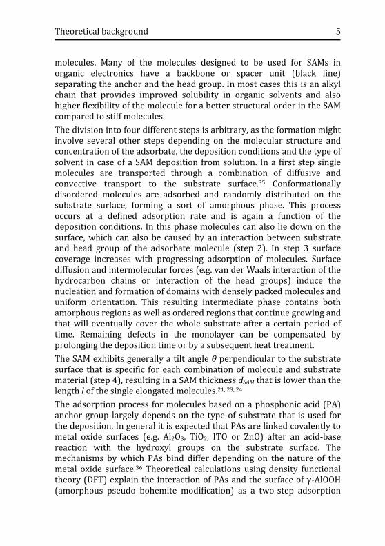
molecules. Many of the molecules designed to be used for SAMs in organic electronics have a backbone or spacer unit (black line) separating the anchor and the head group. In most cases this is an alkyl chain that provides improved solubility in organic solvents and also higher flexibility of the molecule for a better structural order in the SAM compared to stiff molecules. The division into four different steps is arbitrary, as the formation might involve several other steps depending on the molecular structure and concentration of the adsorbate, the deposition conditions and the type of solvent in case of a SAM deposition from solution. In a first step single molecules are transported through a combination of diffusive and convective transport to the substrate surface.35 Conformationally disordered molecules are adsorbed and randomly distributed on the substrate surface, forming a sort of amorphous phase. This process occurs at a defined adsorption rate and is again a function of the deposition conditions. In this phase molecules can also lie down on the surface, which can also be caused by an interaction between substrate and head group of the adsorbate molecule (step 2). In step 3 surface coverage increases with progressing adsorption of molecules. Surface diffusion and intermolecular forces (e.g. van der Waals interaction of the hydrocarbon chains or interaction of the head groups) induce the nucleation and formation of domains with densely packed molecules and uniform orientation. This resulting intermediate phase contains both amorphous regions as well as ordered regions that continue growing and that will eventually cover the whole substrate after a certain period of time. Remaining defects in the monolayer can be compensated by prolonging the deposition time or by a subsequent heat treatment. The SAM exhibits generally a tilt angle θ perpendicular to the substrate surface that is specific for each combination of molecule and substrate material (step 4), resulting in a SAM thickness dSAM that is lower than the length l of the single elongated molecules.21, 23, 24 The adsorption process for molecules based on a phosphonic acid (PA) anchor group largely depends on the type of substrate that is used for the deposition. In general it is expected that PAs are linked covalently to metal oxide surfaces (e.g. Al2O3, TiO2, ITO or ZnO) after an acid-base reaction with the hydroxyl groups on the substrate surface. The mechanisms by which PAs bind differ depending on the nature of the metal oxide surface.36 Theoretical calculations using density functional theory (DFT) explain the interaction of PAs and the surface of γ-AlOOH (amorphous pseudo bohemite modification) as a two-step adsorption
6 Theoretical background
process.37 In the first step, electrostatics and weak hydrogen bonding lead to physisorption of the molecule at the surface. Subsequently, the acid-base reaction results in chemisorption of the physisorbed species. As shown in Figure 2, the P-OH groups react stepwise with two hydroxyl groups to generate first a monodentate and then a bidentate adsorption complex. From theoretical point of view, the latter configuration is regarded as the most favorable on amorphous aluminum oxide. However, this is in contrast to the results obtained by vibrational spectroscopy (IR), which suggest the formation of a tridentate adsorption complex.38
Figure 2: Acid-base reactions of phosphonic acid group on aluminum oxide surface.
Assuming a bidentate binding mode, theoretical calculations predict surface coverage of 4.3 molecules per square nanometer on β-Al(OH)3 and 4.7 nm-2 on γ-AlOOH. These values are in the range of the maximum packing density N = 4.35 nm-2 for close-packed monolayers of alkyphosphonic acids, which was estimated by the cross-sectional area of the phosphonic acid anchor group.37, 39, 40 The packing density in the self-assembled monolayer does not only depend on the anchor group size but is also dictated by the molecular structure and configuration of the head group and spacer unit. Therefore, thickness dSAM, tilt angle θ and packing density N of the SAM are a function of various interactions that are possible between substrate and the different components (anchor group, spacer unit and head group). For phosphonic acids tilt angles between 15° and 30° are expected depending on the binding mode.39

Theoretical background 7
2.1.3 Characterization of SAMs This chapter will introduce the most common techniques used for SAM characterization. A large number of different characterization techniques have been applied to investigate SAMs. Given the small dimensions and the numerous properties of organic molecules used for self-assembled monolayers, a detailed characterization of SAMs is still challenging and often hampered by the lack of local and lateral resolution. Microscopic techniques such as scanning tunneling microscopy (STM) or atomic force microscopy (AFM) provide a direct image of the molecular structure. These techniques allow the detection of defects or different materials (e.g. molecules) at nanometer scale which makes them ideal tools for the characterization of SAMs. Molecular analysis by STM requires conductive substrates and reasonable tunneling currents through the molecular structures. This limits the technique to very thin or conductive SAMs.21, 41 The AFM uses a cantilever made of silicon or silicon nitride with a sharp tip. The cantilever raster-scans the sample surface while its deflection or oscillation amplitude is measured. This signal is obtained by reflection of a laser beam reflected off the cantilever. Detected changes in cantilever deflection or oscillation are corrected to a setpoint value by actuating the cantilever in z-direction via a feedback-controlled piezo. The corrected signal is then converted into a high resolution topographical map of the surface. The AFM offers different modes to investigate a surface. In contact mode, for instance, the tip physically touches the surface of interest. In tapping mode, the cantilever is driven to oscillate up and down near its resonance frequency.42 Special techniques related to AFM enable the measurement of further surface properties such as elasticity, friction or the surface potential.43, 44 Spectroscopic techniques are based on the interaction between radiation of a specific energy and the irradiated material. Information on the surface coverage, the composition and the structure of SAMs can be obtained. Fourier transform infrared spectroscopy (FTIR) can provide information on the molecular orientation and ordering in a SAM by evaluation of the absorbed infrared light and the shape of the obtained spectrum, respectively. For instance, the peak positions of symmetric and asymmetric stretching modes of CH2 groups give the required information about the molecular order in the monolayers.45

8 Theoretical background
X-ray photoelectron spectroscopy (XPS) is a characterization method that is used to analyze the elemental composition of a sample surface. XPS can provide information on the mass coverage, the surface composition and binding states of SAMs.46, 47 The sample is irradiated with X-rays of a specific wavelength. As a result of the interaction between X-rays and atoms of the sample surface photoelectrons are emitted from the material due to the photoelectric effect. The photoelectrons that are collected in the detector provide information on the elemental composition of the surface as their specific kinetic energy correlates directly with their binding energy in the material.48 Diffraction-based techniques such as grazing-incidence X-ray diffraction (GIXD) are used to characterize the details of the crystallographic structure of thin films.49 Further techniques employed for the analysis of SAMs are low energy electron diffraction (LEED) and X-ray reflectivity (XRR). These methods typically require the use of synchrotron radiation and provide information about electron densities, thickness and roughness at Angstrom resolution.50 The XRR technique provides the specular reflection R(Qz) which is related to the distribution of the electron density in depth ρ(z). The evaluation of the experimental data requires the application of models that take into account certain boundary conditions, such as the roughness, thickness and electron density of the substrate and the thin film. The method is based on a system that is divided into several different layers. The most appropriate model is determined by a systematic fit of these layers and their parameters for the best matching of experimental data and the R(Qz) curve. As a result of the fitting procedure, the obtained scattering length density profile (SLD) shows the electron density distribution perpendicular to the surface in the analyzed film.51, 52 Further techniques that are used for the characterization of SAMs but that were not assigned to one of the above listed classes of methods are ellipsometry, quartz crystal microbalance and wetting experiments. Ellipsometry is employed for the determination of the SAM thickness.50 The quartz crystal microbalance is a tool that is mainly used for the investigation of adsorption kinetics and the surface coverage of SAMs.53 Wetting measurements are a simple but effective technique to determine the surface energy of self-assembled monolayers. A drop of liquid is placed on the surface using a syringe and the contact angle is then determined. Liquids with different polarity are used to calculate the surface energy and its polar and dispersive components from the contact

Theoretical background 9
angle data. Typically, an estimation of the SAM surface coverage and structure can be obtained by the data obtained from the wetting measurements.22-24 Apart from the conventional experimental methods, computational modeling and simulation of organic molecules and their properties have become a powerful technique to complement and to verify experimental results obtained by other techniques. Molecular dynamics (MD) and density functional theory (DFT) are readily available methods to simulate and to calculate different properties of SAMs.54
2.1.4 Electronic properties of SAMs SAMs have become a very attractive component in organic electronic devices due to their large versatility regarding the modification and optimization of interfaces. Two main application routes can be identified that originate from the electrical properties of the molecules used for the SAM system. SAMs with semiconducting groups (e.g. fullerenes) are interesting for applications that require an enhanced charge transfer at an interface. On the other hand, when it comes to optimizing the interface with an insulating material (e.g. the dielectric in organic thin-film transistors), molecules with good insulating properties are required. SAMs made of alkyl trichlorosilanes exhibit very low leakage currents (4 − 5 orders of magnitude lower than silicon dioxide of equivalent thickness). That made alkyl SAMs a potential candidate for device applications as high performance insulators at nanometer scale.32, 55 Similar SAMs based on the trichlorosilane anchor group have been applied as dielectric in OTFTs and have led to the reduction of the operating voltage and power dissipation in such devices thanks to their large capacitance compared to silicon dioxide.15 Charge conduction through SAMs can be described by different theoretical models. Nonresonant tunneling is the most common transport mechanism observed for insulating, saturated alkyl SAMs.56-58 In the simplest model the SAM can be regarded as a finite potential barrier ΦB that can be overcome completely (direct tunneling) or partially (Fowler-Nordheim tunneling) by electrons (cf. Figure 3). It is important to note that the actual tunneling mechanism depends on several conditions, such as temperature, applied voltage and conformation, type and thickness of the SAM. For instance, charge conduction through π-conjugated molecular SAMs may be described with near-resonant tunneling through the molecular orbitals.56, 58-60

10 Theoretical background
Further conduction mechanisms, such as thermionic emission, Poole-Frenkel emission and hopping conduction show temperature dependence, while both direct and Fowler-Nordheim tunneling are temperature independent. In general, the different models describe the relationship between tunneling current, the applied voltage and the shape of the electrical barrier. Detailed descriptions of the models can be found in literature.45, 56
Figure 3: SAMs described as potential barriers in energy band diagrams for direct and Fowler-Nordheim tunneling mechanisms.
Other applications require SAMs that enhance the electronic transfer at an interface, e.g. in case of electron injection from electrodes into the semiconductor. In such cases dipolar SAMs are typically used to reduce the barrier height for charge injection. A popular example for the versatility of SAMs in organic electronics is the modification of gold electrodes with functionalized thiols in OTFTs. It has been shown that this procedure allows the optimization of both electron as well as hole injection into the semiconductor by control of the molecular dipoles and the reduction of the contact resistance at the interface.61, 62 The ability of SAMs to tune injection barriers relies on their electrostatic potential. Every adsorbed species that exhibits a permanent dipole moment perpendicular to the surface µ⊥ causes a change of the work function ∆φ of the substrate material according to the Helmholtz equation.2, 63
Further properties of the SAM, such as the relative permittivity εSAM, the packing density N and the tilt angle of the SAM θ have an impact on the
ΦΒ ΦΒ
Direct Fowler-Nordheim
∆𝝓 =𝒒 ∙ 𝑵 ∙ 𝝁⊥𝜺𝟎 ∙ 𝜺𝑺𝑨𝑴
(1)

Theoretical background 11
magnitude of the work function change. ε0 is the permittivity of free space and q the elementary charge. Figure 4 illustrates the origin of a permanent molecular dipole moment using the example of chloromethane. The difference in electronegativity of the carbon atom and the chlorine atom leads to intramolecular charge separation and to an individual bond moment, as indicated by the partial charges δ+ and δ-. The total dipole moment µ of a molecule corresponds to the sum of all individual bond moments.64
Figure 4: Permanent molecular dipole moment µ of chloromethane. The arrow shows the direction of the total dipole moment in this two dimensional projection.
Bruening et al. studied functionalized disulfide ligands forming SAMs on gold and CuInSe2 and compared experimental work function values obtained from contact potential difference (CPD) measurements with calculated values obtained by the Helmholtz equation.65 The layers were characterized with ellipsometry, electrochemistry and FTIR spectroscopy to obtain the information about SAM thickness, surface coverage and orientation. The results confirmed the possibility to predict changes of the work function by determining the SAM parameters on the right-hand side of Equation (1).65, 66 In a study carried out by Ellison et al., SAM dipoles calculated from experimental results obtained from Kelvin Probe Force Microscopy (KFM) differed significantly from values estimated for the individual molecules with a semiempirical quantum chemistry program (MOPAC).43 An explanation for this finding could be a reduction of the layer dipole moment because of screening and depolarization effects due to dipole-dipole interactions in the SAM. Consequently, computed molecular dipole moments for single molecules would overestimate the experimental layer dipole.43, 67 These effects were described by Cahen et al. as cooperative effects that become significant when the molecules form well-oriented and closely packed layers. If the distance between two molecules in the layer is smaller than the length of the dipole, and if the size of the molecular domains is much larger than the dipole length,

12 Theoretical background
then the system can be approximated to behave as an infinite 2D dipole layer with uniform electrostatic drop over the width of the layer.68 Such dipole layers have properties that differ significantly from those of a mere collection of isolated molecules. For instance, there is strong evidence that SAM formation induces a charge-transfer process that redistributes charge within the molecules forming the SAM and that may result in a smaller layer dipole.43, 68 Depolarization, a process well known in atomic surface physics, implies a charge transfer between adsorbate and the substrate. This is shown schematically for a SAM in Figure 5.
Figure 5: Schematic illustrating the redistribution of charges in SAMs as a result of depolarization.68

Theoretical background 13
2.2 Optical excitation of organic materials
Organic compounds, especially those with a high degree of conjugation, absorb light in the UV or visible regions of the electromagnetic spectrum, which is caused by the promotion of an electron from one orbital (usually ground-state) to a higher orbital. The amount of energy necessary to make this transition depends mostly on the nature of the two orbitals involved and the degree of conjugation in the molecule. Functional groups that cause absorption are called chromophores and can be detected through analysis of the absorbance spectrum in a spectrophotometer.64, 69 The different excited states of organic molecules are difficult to measure because of their generally short lifetimes. But if accurately analyzed, differences from the ground state can be detected as changes of the molecular geometry, dipole moment, and acid or base strength. An excited state can drop to the ground state by giving off the energy difference between the two states in the form of light or heat, depending on the type of excited state and physical pathway of the deactivation. Fluorescence and phosphorescence are two important effects related to optical excitations of organic molecules that can be detected and used for the analytics of such materials. Another important effect in the field of organic electronics and particularly in organic optoelectronics is photosensitization. This effect describes the transfer of excess energy from the excited molecule to another molecule in the environment. The excited molecule, called donor, thus drops to ground state while the other molecule, called acceptor, becomes excited.64 In an organic solar cell, the charge transfer of an excited donor to the acceptor leads to the generation of a photocurrent that can be collected at the electrodes. This process is called the photovoltaic effect and is explained in more detail in Chapter 2.3.5. The occurrence of the photovoltaic effect in OTFTs is discussed in Chapter 2.3.4. In Chapters 5 and 6, it will be demonstrated how photoactive SAMs can be used to modify and optimize the function of photosensitive OTFTs and OSCs.

14 Theoretical background
2.3 Electronic devices
2.3.1 Capacitor A capacitor is a passive electrical component used to store energy electrostatically in an electric field. In its simplest version a capacitor is built up with two parallel conductor plates and a dielectric placed in between the plates, as depicted in Figure 6(a). The capacitance C of a parallel plate capacitor is defined by
with εo as the permittivity of free space, εr the relative permittivity of the dielectric material, A as the area of the electrodes and d as the thickness of the dielectric layer. In this work, capacitor devices are mainly used to characterize the dielectric properties of SAMs. The layout of a capacitor device with a hybrid dielectric consisting of aluminum oxide and a SAM is shown in Figure 6(b).
Figure 6: Schematics of parallel plate capacitors: with dielectric layer of thickness d and relative permittivity εr (a), and with a hybrid dielectric composed of AlOx and a SAM connected in series (b).
In a simplified model, both components of the hybrid dielectric can be regarded as single capacitors connected in series. The total capacitance Ctotal of the hybrid dielectric can then be calculated according to
Dielectric
Top Contact
Bottom Contact
εrd
CSAM
CAlOx
(a) (b)Top Contact
Bottom Contact
AlOx
𝑪 = 𝜺𝟎 ∙ 𝜺𝒓 ∙𝑨𝒅 (2)
𝟏𝑪𝒕𝒐𝒕𝒂𝒍
=𝟏
𝑪𝑨𝒍𝑶𝒙+
𝟏𝑪𝑺𝑨𝑴
(3)

Theoretical background 15
Consequently, measuring the total capacitance Ctotal of the capacitor devices shown in Figure 6(b) allows the calculation of the permittivity of the SAM if the capacitance of the aluminum oxide layer CAlOx and the thickness dSAM of the SAM are known. Charges accumulate at each side of the dielectric when an electrical potential between the top and bottom contacts is applied. Each contact holds opposite and equal amounts of charges, which leads to the formation of an electric field in the dielectric. The amount of charges Q that can be stored in the capacitor element is directly proportional to the capacitance C and the potential V applied between the two plates.
2.3.2 Organic thin-film transistor Transistors are three-terminal devices in which the resistance of a semiconductor between two of the contacts (source and drain) is controlled by the third (gate). A field-effect transistor (FET) is a transistor where the channel resistance is controlled capacitively by an electric field. An example is the MOSFET (metal-oxide-semiconductor field-effect transistor), which is the most important device for integrated circuits used in microprocessors. A thin-film transistor (TFT) is a FET in which all layers are deposited as a thin film. Typical thin films, such as amorphous silicon, exhibit a higher density of defects and interface traps, which is the reason for the lower performance of TFTs compared to conventional FETs. The same applies for organic thin-film transistors (OTFTs) where one or more of the active layers consist of organic materials.70 A schematic layout of OTFT devices used in this work is shown in Figure 7. The transistor channel is defined by the width W of the electrodes and the distance L between the electrodes. The electric field induced by applying a potential between source and gate electrode results in accumulation of charge carriers in the semiconductor at the interface to the dielectric. The voltage VGS, applied between the two electrodes, allows for the modulation of the charge carrier density in the semiconductor close to the interface.
𝑸 = 𝑪 ∙ 𝑽 (4)

16 Theoretical background
Figure 7: Schematic layout of an OTFT device.
The accumulation of holes is visualized exemplarily for a p-type semiconductor in Figure 8. The energy band model was originally established to describe electronic states of inorganic materials, such as Si or GaAs and was adapted to organic semiconductor materials. Due to the molecular structure of these materials charge transport in organic semiconductors can be described in the energy band model more adequately by replacing conductive and valence band with lowest unoccupied molecular orbital (LUMO) and highest occupied molecular orbital (HOMO), respectively.71
Figure 8: Energy band diagram of a MIS capacitor under flat-band condition (a). In (b) a negative bias is applied shifting the electrode´s Fermi level towards higher energy and bending the HOMO and LUMO level of the semiconductor.
Substrate
Gate
Dielectric
Semiconductor
Source DrainL
WVGS
VDS
LUMO
HOMO
Ef V <0G
(a) (b)Vacuum level
φm
χ
Eg Ei

Theoretical background 17
Figure 8(a) shows a simplified band diagram for an ideal MIS (metal-insulator-semiconductor) capacitor. In this case the bands of a p-type semiconductor are flat for zero applied voltage and the following equation for the flat-band potential VFB is fulfilled.72
with φm as the metal workfunction, χ the electron affinity, Eg the bandgap and φf the potential difference between the Fermi level Ef and the intrinsic Fermi level Ei of the organic semiconductor. Applying a negative voltage to the electrode leads to an upward band bending at the interface and to accumulation of the majority charge carriers which in case of a p-type semiconductor corresponds to holes (Figure 8(b)). Voltages of opposite sign result in depletion of holes and accumulation of minority charge carriers (electrons) in the LUMO (not shown in Figure 8). In order to obtain a constant supply of electric current, a potential between source and drain electrode VDS has to be applied. The electric field between both electrodes leads to charge carrier injection into the semiconductor at the source electrode and charge carrier extraction at the drain electrode, as shown in Figure 9(a) for a p-type semiconductor.
Figure 9: Principle of charge carrier injection and transport in the semiconductor of an operating transistor (a), and layout of an OTFT with a patterned gate electrode with channel length L and overlap ΔL (b).
A crucial aspect for the performance of a transistor is the device layout. In general, patterning of the semiconductor layer improves the performance by reducing parasitic currents. Another important layout feature is the overlap of gate and source/drain electrodes (ΔL) shown in Figure 9(b). Reducing the overlap results in lower leakage currents and improved switching behavior of the device.73 Another possibility to tune
Source Drain
Substrate
Gate
Dielectric
Gate
Substrate
L∆L ∆L(a) (b)
𝑽𝑭𝑩 = 𝝓𝒎 − 𝝌 +𝑬𝒈𝟐𝒒 + 𝝓𝒇 = 𝟎 (5)

18 Theoretical background
transistor performance is to change the order of the layers. The top-contact bottom-gate approach shown in Figure 9 has the advantage of a large contact area between electrode and semiconductor. On the other hand, charges injected into the transistor channel have to pass first the whole thickness of the semiconductor layer to reach the interface to the dielectric. For characterization of transistor devices two main measurement setups are used. In the transfer characteristic the drain current ID is measured as a function of VGS at a constant VDS. In Figure 10(a) the transfer characteristic of a p-type OTFT is depicted. At positive bias the hole density near the interface is very low, hence the drain current is at a very low level. As the bias is swept to more negative voltage, holes begin to accumulate near the interface. At a critical charge carrier density the drain current starts to increase abruptly and the transistor is switched on. The diagram shows two curves recorded at different VDS.
Figure 10: Transfer characteristic of a p-type OTFT at two different constant drain-source voltages (a). The output characteristic shows the progression of the drain current at a constant gate-source voltage and an increasing drain-source voltage. The dashed line indicates the range of linear and saturation regime.
Depending on the value of VDS the device will operate either in the linear (at low |VDS|) or in the saturation regime (at high |VDS|). The transition between linear and saturation regime can be regarded as a third regime. The existence of the three regimes is a cause of the concurrence of the two electric fields which determine the charge carrier distribution in the channel. A more detailed description can be found in Reference [74]. In the output characteristic the drain current is plotted as a function of VDS at a constant VGS (see Figure 10(b)). The dashed line in the diagram
(a) (b)

Theoretical background 19
indicates the classification of linear and saturation regimes. In the linear regime the drain current characteristic can be described by:
In the saturation regime ID can be described by:
with µ as the field-effect mobility, VTH as the threshold voltage and W as the width and L the length of the transistor channel (Figure 7). The normalized capacitance Ci is given by:
Most of the transistor parameters can be extracted from the transfer measurement curves, as depicted exemplarily in Figure 11 for a p-type semiconductor. The ON/OFF current ratio is the ratio between the drain current in the ON-state at maximum VGS and the drain current in the OFF-state. A large ON/OFF ratio is desirable for a clear distinction between the two states and the application as a logical switch. Similarly, a high ratio of drain current and gate current ID/IG in the ON-state is an important criterion for a well-performing transistor device. A low gate (or leakage) current indicates a good isolating behavior of the dielectric. The shift between drain current characteristic in the forward measurement (from positive to negative bias) and the backward measurement (from negative to positive bias) is referred to as hysteresis and is related mainly to defect states near the interface of semiconductor and dielectric. These defects act as charge trapping sites and hinder the lateral charge carrier transport in the transistor channel.
𝑰𝑫 = 𝝁 ∙ 𝑪𝒊 ∙𝑾𝑳 ∙ (𝑽𝑮𝑺 − 𝑽𝑻𝑯) ∙ 𝑽𝑫𝑺 (6)
𝒇𝒐r 𝑽𝑫𝑺 << 𝑽𝑮𝑺 − 𝑽𝑻𝑯
𝑰𝑫 = 𝝁 ∙ 𝑪𝒊 ∙𝑾𝟐 ∙ 𝑳 ∙
(𝑽𝑮𝑺 − 𝑽𝑻𝑯)𝟐 (7)
𝒇𝒐𝒓 𝑽𝑫𝑺 ≥ 𝑽𝑮𝑺 − 𝑽𝑻𝑯
𝑪𝒊 =𝜺𝟎 ∙ 𝜺𝒓𝒅 (8)

20 Theoretical background
Figure 11: Plot of drain, gate and square-root of drain current as a function of the gate-source voltage indicating the parameters that can be extracted from the transfer characteristic.
An important parameter for characterization of the transistor performance is the field-effect mobility µ. It can be inferred from the transistor characteristic and is directly related to the drain current as suggested by Equations (6) and (7). The most widespread technique is plotting the square root of the saturation drain current as a function of the gate-source voltage at high VDS. The slope m of the square root of drain current can be defined as:
At VGS much larger than VTH Equation (7) can be rewritten and solved for the mobility:
The threshold voltage VTH is obtained from the interception of the linear fit of the square root of drain current and the gate-source voltage axis. The use of this parameter is adopted from conventional MOSFETs. Although the operation mechanisms in transistors based on silicon differ significantly from those based on organic materials, the parameter VTH is widely used to characterize the turn-on behavior of OTFTs and is defined
VTH
VON
OFF-State
ON-State
HysteresisSlope m
𝒎 = 𝝏𝑰𝑫𝝏𝑽𝑮𝑺
(9)
𝝁 =𝟐 ∙ 𝑳
(𝑾 ∙ 𝑪𝒊)∙ 𝒎𝟐 =
𝟐 ∙ 𝑳(𝑾 ∙ 𝑪𝒊)
∙ 𝝏𝑰𝑫𝝏𝑽𝑮𝑺
𝟐
(10)

Theoretical background 21
as the minimum source-gate voltage required to obtain a reasonable drain current. Another parameter used in literature to characterize the turn-on behavior of organic transistors is the turn-on (or switch-on) voltage VON. As depicted in Figure 11, VON is the voltage at which the drain current starts to increase exponentially. Below the turn-on voltage the drain current is limited by charge leakage through the semiconductor, through the gate dielectric, or across the substrate surface.73 The region that extends between VON and VTH is denominated as the subthreshold region. The subthreshold slope (or subthreshold swing) S is defined as:
S is a measure for the quality of the interface of semiconductor and dielectric as it is directly related to the density of interfacial trap states Nit (k is the Boltzmann constant, T is the temperature and q the electronic charge). Silicon MOSFETs with low interface trap densities have S values close to the ideal room-temperature subthreshold swing of 60 mV/dec while OTFTs exhibit typically larger S values due to larger interface trap densities.70 It is important to note that the operation of transistors depends on the frequency of the applied signal. The frequencies demanded for the envisioned applications of OTFTs, such as active-matrix displays, are typically below 100 kHz.75, 76 However, operation of OTFTs with cutoff frequencies of a few MHz for more demanding applications has already been demonstrated.77 The main limitation of the cutoff frequency is the rather low charge carrier mobility of organic semiconductors.
2.3.3 Concept of threshold voltage in OTFTs and the role of interfacial dipoles
The concept of threshold voltage is defined specifically for silicon MOSFETs and is based on the formation of an inversion layer at the dielectric-semiconductor interface (i.e. the density of minority charge carriers exceeds that of majority charge carriers). For OTFTs this is not the case, as they operate in accumulation mode where no inversion layer is formed.72, 78 The origin of a threshold voltage is ascribed mainly to the occurrence of trap states that have to be filled before the charge carriers induced by the field-effect can be mobile in the transistor channel.
𝑺 =𝒌𝑻𝒒 𝒍𝒏𝟏𝟎𝟏 +
𝒒𝑵𝒊𝒕
𝑪𝒊 (11)

22 Theoretical background
According to Equation (7) the square-root of the saturation drain current as function of the gate voltage should result in a straight line. However, for OTFTs this is usually not the case, as can be noticed from the upward curvature at low gate voltages in the characteristic shown in Figure 11. This behavior is related to the nature of the organic semiconductors and to the larger trap density in OTFT devices resulting for instance in large contact resistances and gate voltage dependent mobilities. These effects have an impact on the turn-on behavior and thus on the practical extraction of the threshold voltage that involves arbitrary selection of the fit region for the linear regression line around the inflection point. This has to be born in mind when using the threshold voltage as parameter to characterize and to compare different transistor devices. For this reason, using the turn-on voltage VON for these purposes can be more appropriate in some cases. Using the above described extraction method of VTH for OTFT characterization constitutes rather a compromise due to the lack of other characterization approaches. An alternative VTH extraction method for MOSFETs has been presented by Wong and coworkers. Their method consists of plotting the second derivative of the linear drain current as a function of gate voltage and is called transconductance change (TC) method.74, 79 If constant charge carrier mobility µ is assumed, then the threshold voltage of an OTFT may be defined by:
In Equation (12), the threshold voltage VTH is the gate voltage for which the channel conductance is equal to that of the whole semiconducting layer, with q as the elemental charge, n as the charge carrier density, dc the channel thickness and Ci the insulator capacitance.78 Note that this expression does not account for built-in potentials that contribute to the threshold voltage. For instance, the flat-band potential VFB (introduced in Equation (5) for the MIS capacitor) accounts for any work-function difference between the semiconductor and the gate.70, 72 Further contributions to VTH can be caused by built-in dipoles (e.g. of a SAM) impurities and interface states, so that the effective threshold voltage will be the sum of all contributions arising from electrostatic effects in the bulk and the interfaces of the device.80 The superposition of the different contributions makes it difficult to determine and to predict the exact value of each contribution due to the
𝑽𝑻𝑯 = ±𝒒 ∙ 𝒏 ∙ 𝒅𝒄
𝑪𝒊 (12)

Theoretical background 23
lack of characterization methods and analytical expressions for the different contributions. However, for well-oriented and closely-packed SAMs a uniform electrostatic drop over the width of the dipole layer can be assumed so that according to the Helmholtz equation we can define the following relationship for the electrostatic potential of a SAM (cf. Equation (1)):
Here, µz represents the z-component of an isolated SAM molecule. It is assumed that the effective dipole moment of the SAM with tilt angle θ corresponds to the term µz × cosθ. This suggests that a SAM formed of molecules with a distinct dipole moment perpendicular to the substrate surface (µz × cosθ) leads to a shift of the threshold voltage VTH due to its electrostatic potential VSAM (cf. Figure 12). This potential can either generate mobile charge carriers in the semiconductor channel or withdraw them, depending on the direction of the dipole.81
Figure 12: Principle of threshold voltage shift due to the dipole moment of a SAM. The dipole moment has a direct effect on the charge carrier density in the semiconductor and leads to a reduction of mobile holes for a SAM dipole moment pointing away from the semiconductor (left) and to an additional accumulation of mobile holes for a SAM dipole moment pointing towards the semiconductor (right).
In 2004, Kobayashi et al. and Pernstich et al. used organosilanes with different functional groups on SiO2 as the dielectric in OTFTs.82, 83 They indeed observed that the electrical properties of OTFTs could be changed by the nature of the applied SAM molecules and that the threshold
-3 -2 -1 0 10
2x10⁻⁴
4x10⁻⁴
6x10⁻⁴
8x10⁻⁴
VDS = -1V
Gate-source voltage (V)
Squa
re ro
ot o
f dra
in c
urre
nt (√
A)
VTH VTH
VTH shift
µz
µz
Source Drain
SubstrateGate
Dielectric
Source Drain
SubstrateGate
Dielectric
𝑽𝑺𝑨𝑴 =𝑵 ∙ 𝝁𝒛 ∙ 𝒄𝒐𝒔𝜽𝜺𝟎𝜺𝑺𝑨𝑴
(13)

24 Theoretical background
voltage shifted qualitatively according to the direction of the dipole moment of the applied SAM molecules. The topic of SAM induced threshold voltage shifts was discussed controversially in the studies that followed. Device simulations indicated that the dipolar contributions were too small to explain the large VTH shifts that were observed experimentally.84 None of the experimental studies could confirm the predictive power of Equation (13) which relates the dipole moment µz of a molecule to the electrostatic potential of its SAM. Instead, it was reported that other effects, such as space charge layers, residual charge carriers or trapped charges in the dielectric, had a considerable impact on the shift of the threshold voltage.84-86 Thus, the mechanisms responsible for the SAM induced threshold voltage shift remained under debate. In 2012, Gholamrezaie et al. reported that the VTH shifts could not originate from the SAMs dipolar character by applying Scanning Kelvin-Probe Microscopy (SKPM).86 They exfoliated the semiconductor of OTFTs in order to measure the surface potentials of the SAMs after electrical characterization of the devices. From the comparison of the surface potential of freshly prepared SAMs on the one hand and SAMs that had been electrically stressed during the device operation on the other hand, they concluded that charges trapped in the SAM had to be responsible for the VTH shifts.
2.3.4 Organic phototransistor Phototransistors are devices that combine the functions of light detection, photocurrent modulation and electrical field controlled switching. The ease of integration into electronic circuits and their comparably high photosensitivity made phototransistors based on silicon the preferred light detector choice over conventional photodiodes.87, 88 The first organic phototransistors were presented by Narayan’s group in 2001.88, 89 The functionality of organic phototransistors is based on the combination of two effects. The photovoltaic effect (i.e generation of a photocurrent due to charge separation of charge carriers at a donor-acceptor interface) leads to a photocurrent in the ON-state operation of the transistor, while the photoconductive effect is responsible for the transistor´s photocurrent in the OFF-state.90 The threshold voltage shift observed in light responsive transistors is strongly related to trapping of photoinduced charges at the semiconductor/dielectric interface and is a

Theoretical background 25
direct consequence of the photoconductive and photovoltaic effects, as shown in Figure 13.91-93
Figure 13: Transfer characteristics for p-type OTFT in the dark and under illumination. The increase of the OFF-current (photoconductive effect) and the shift of the characteristic (photovoltaic effect) are indicated by red arrows.
It is assumed that the photocurrent in the OFF-state is generated due to photogenerated electrons trapped in the dielectric, while holes can move freely in the p-type channel. Additional holes are supplied by the source to compensate for the trapped electrons and thus lead to the increase of OFF-current (photoconductive effect). Trapping of electrons also leads to a shift of the characteristic towards more positive VGS (photovoltaic effect). The name of the effect indicates that an internal voltage difference between the channel and the bulk of the transistor is created by the separation of photogenerated holes and electrons.93 The most important parameters for phototransistors are the responsivity Rlight defined as
and the photosensitivity Plight defined as
-3 -2 -1 0 1 210-14
10-12
10-10
10-8
10-6
Gate-source voltage (V)
dark illuminated
Gat
e cu
rren
t (A)
Dr
ain
curr
ent (
A)
1
2
1
2
Photoconductiveeffect
Photovoltaiceffect
𝑹𝒍𝒊𝒈𝒉𝒕 = 𝑰𝒍𝒊𝒈𝒉𝒕 − 𝑰𝒅𝒂𝒓𝒌
𝑷𝒊𝒍𝒍 (14)
𝑷𝒍𝒊𝒈𝒉𝒕 = 𝑰𝒍𝒊𝒈𝒉𝒕 − 𝑰𝒅𝒂𝒓𝒌
𝑰𝒅𝒂𝒓𝒌 (15)
26 Theoretical background
where Ilight is the drain current under illumination, Idark the drain current under dark conditions and Pill the incident illumination power. The responsivities of the first organic devices employing a single layer of poly(3-octylthiophene-2,5-diyl) (P3OT) as the photoactive semi-conductor were quite low (≈ 1 A/W).88 In the subsequent studies that employed conjugated polymer/fullerene blends and highly photo-sensitive biphenyl end-capped fused bithiophene oligomers R-values of 5 A/W and up to 82 A/W were reached, respectively.94, 95
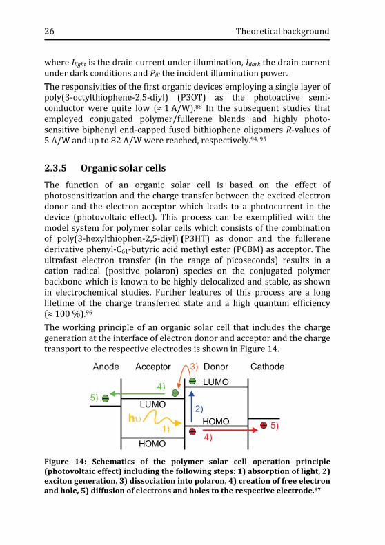
2.3.5 Organic solar cells The function of an organic solar cell is based on the effect of photosensitization and the charge transfer between the excited electron donor and the electron acceptor which leads to a photocurrent in the device (photovoltaic effect). This process can be exemplified with the model system for polymer solar cells which consists of the combination of poly(3-hexylthiophen-2,5-diyl) (P3HT) as donor and the fullerene derivative phenyl-C61-butyric acid methyl ester (PCBM) as acceptor. The ultrafast electron transfer (in the range of picoseconds) results in a cation radical (positive polaron) species on the conjugated polymer backbone which is known to be highly delocalized and stable, as shown in electrochemical studies. Further features of this process are a long lifetime of the charge transferred state and a high quantum efficiency (≈ 100 %).96 The working principle of an organic solar cell that includes the charge generation at the interface of electron donor and acceptor and the charge transport to the respective electrodes is shown in Figure 14.
Figure 14: Schematics of the polymer solar cell operation principle (photovoltaic effect) including the following steps: 1) absorption of light, 2) exciton generation, 3) dissociation into polaron, 4) creation of free electron and hole, 5) diffusion of electrons and holes to the respective electrode.97
LUMO
HOMO
LUMO
HOMO
Acceptor DonorAnode Cathode
hυ1)
2)
3)
4)
4)
5)
5)

Theoretical background 27
The most important characterization tool for a solar cell is the determination of the current density (j)-voltage (V) behavior. Typically, for each characterization the dark as well as the illuminated characteristic was measured. A representative j-V characteristic under illumination is shown in Figure 15 together with the typical diode behavior in the dark.
Figure 15: j-V-characteristic of an organic solar cell with key parameters.
The most important features in the j-V characteristic of a solar cell are the short circuit current density (jSC), open-circuit voltage (VOC) and the maximum power point (MPP). Further important parameters are the fill factor FF defined as:
with jMP as the current density and VMP as the voltage at maximum power point, respectively. If the solar cell characteristics are measured under standardized conditions with a solar simulator, the power conversion efficiency PCE can be defined as:
PIN is the incident light intensity measured by a calibrated reference cell and M is the spectral mismatch factor that accounts for deviations in the
-0.2 0 0.2 0.4 0.6 0.8-10
-5
0
5
10
15
20 dark illuminated
Curre
nt d
ensi
ty (m
A/cm
²)
Voltage (V)
VMPVOC
MPP
jSC
jMP
𝑭𝑭 = 𝒋𝑴𝑷 ∙ 𝑽𝑴𝑷𝒋𝑺𝑪 ∙ 𝑽𝑶𝑪
(16)
𝑷𝑪𝑬 = 𝒋𝑺𝑪 ∙ 𝑽𝑶𝑪 ∙ 𝑭𝑭
𝑷𝑰𝑵∙ 𝑴 (17)

28 Theoretical background
spectral output of the solar simulator with respect to the standard AM1.5 spectrum. The parallel resistance RP and the serial resistance RS of the solar cell under dark conditions are the inverse values of the slope at jSC and VOC, respectively.
Experimental 29
3. Experimental
3.1 Substrates and device layout
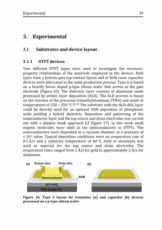
3.1.1 OTFT devices Two different OTFT types were used to investigate the structure-property relationships of the materials employed in the devices. Both types have a bottom-gate top-contact layout and in both cases capacitor devices were fabricated in the same production process. Type A is based on a heavily boron doped p-type silicon wafer that serves as the gate electrode (Figure 16). The dielectric layer consists of aluminum oxide processed by atomic layer deposition (ALD). The ALD process is based on the reaction of the precursor trimethylaluminum (TMA) and water at temperatures of 250 – 350 °C.98, 99 The substrate with the ALD-AlOx layer could be directly used for an optional SAM deposition of phosphonic acids yielding a hybrid dielectric. Deposition and patterning of the semiconductor layer and the top source and drain electrodes was carried out with a shadow mask approach (cf. Figure 17). In this work small organic molecules were used as the semiconductors in OTFTs. The semiconductors were deposited in a vacuum chamber at a pressure of < 10-6 mbar. Typical deposition conditions were an evaporation rate of 0.1 Å/s and a substrate temperature of 60 °C. Gold or aluminum was used as material for the top source and drain electrodes. The evaporation rates ranged from 1 Å/s for gold to approximately 2 Å/s for aluminum.
Figure 16: Type A layout for transistor (a) and capacitor (b) devices processed on a p-type silicon wafer.
Drain (Au)Source (Au)
Gate (p-type Si)ALD-AlOx
SAMSemiconductor
(a) (b)

30 Experimental
Type B transistors were fully patterned on a heavily doped p-type silicon wafer with 100 nm thermally grown silicon dioxide. The first step in the fabrication of the bottom-gate top-contact transistors was the formation of the gate electrode by thermal evaporation of 30 nm aluminum through a shadow mask.
Figure 17: Fabrication of a transistor with the shadow mask technique; the arrow indicates the direction of the mask shift for the step-wise patterning of the different functional layers.
In layout B the aluminum oxide dielectric layer was generated by plasma treatment in oxygen atmosphere at a pressure of 0.2 mbar and a duration of 3 minutes in a Diener Electronic Pico device (200 W). The thickness of the aluminum oxide that could be achieved with this type of plasma treatment was approximately 3.6 nm.16 Hybrid dielectrics were formed optionally by subsequent immersion in a SAM solution. For the deposition of the structured semiconductor layer the mask has to be fixed on the processed substrate according to the scheme shown in Figure 17 so that the semiconductor layer could be evaporated onto the gate dielectric. The evaporation conditions for the semiconductor and the top contacts were the same as described for layout Type A. The measures of the transistor channels were identical for both types of transistor devices with channel lengths of 10 µm, 20 µm and 40 µm and widths of 150 µm, 300 µm and 600 µm, respectively.
Figure 18: Type B layout for transistor (a) and capacitor (b) devices processed on a p-type silicon wafer with 100 nm thermally grown silicon dioxide.
1. gate
2. semiconductor
3. source-drain
Gate (Al)AlOx
SAMSemiconductor
Drain (Au)Source (Au)(a) (b)

Experimental 31
3.1.2 OSC devices The typical layout used for the investigation of SAMs in organic solar cells was an inverted structure as depicted in Figure 19. Different approaches with aluminum doped zinc oxide (AZO) nanoparticles, spray coated zinc oxide (ZnO) nanorod layers and titanium dioxide (TiO2) nanotubes used as the electron extraction layer (EEL) were tested in this work. The SAMs were applied as modifiers of the EEL metal oxide layers. Either neat poly(3-hexylthiophen-2,5-diyl) (P3HT) or the blend of P3HT and phenyl-C61-butyric acid methyl ester (PCBM) were applied as the active layer. Poly(3,4-ethylenedioxythiophene) poly(styrenesulfonate) (PEDOT:PSS) was used as the hole extraction layer (HEL). A 100 nm thick Ag layer was thermally evaporated to form the top electrode. The active area of the investigated devices was 10.4 mm².
Figure 19: Layout of an inverted organic solar cell.
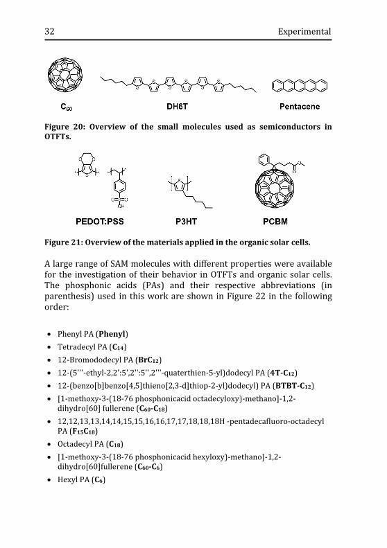
3.2 Materials
The molecules applied as semiconductors in OTFTs were fullerene-C60 (C60), α,ω-dihexylsexithiophene (DH6T) and pentacene (cf. Figure 20). C60 (sublimed, 99.9 %) and pentacene were purchased from Aldrich. Pentacene was purified by gradient sublimation at the Experimental Physics Institute of University Würzburg (AG Pflaum). DH6T was obtained from Heraeus Precious Metals. The active materials in the organic solar cells were P3HT and PCBM. PEDOT:PSS was used as hole extraction layer material (cf. Figure 21). P3HT was purchased from Merck, technical grade PCBM from Solenne and PEDOT:PSS (Clevios PH) from H.C. Starck.
GlassAnode
Active layer
HELCathode
EEL
32 Experimental
Figure 20: Overview of the small molecules used as semiconductors in OTFTs.
Figure 21: Overview of the materials applied in the organic solar cells.
A large range of SAM molecules with different properties were available for the investigation of their behavior in OTFTs and organic solar cells. The phosphonic acids (PAs) and their respective abbreviations (in parenthesis) used in this work are shown in Figure 22 in the following order: • Phenyl PA (Phenyl) • Tetradecyl PA (C14) • 12-Bromododecyl PA (BrC12) • 12-(5'''-ethyl-2,2':5',2'':5'',2'''-quaterthien-5-yl)dodecyl PA (4T-C12) • 12-(benzo[b]benzo[4,5]thieno[2,3-d]thiop-2-yl)dodecyl) PA (BTBT-C12) • [1-methoxy-3-(18-76 phosphonicacid octadecyloxy)-methano]-1,2-
dihydro[60] fullerene (C60-C18) • 12,12,13,13,14,14,15,15,16,16,17,17,18,18,18H -pentadecafluoro-octadecyl
PA (F15C18) • Octadecyl PA (C18) • [1-methoxy-3-(18-76 phosphonicacid hexyloxy)-methano]-1,2-
dihydro[60]fullerene (C60-C6) • Hexyl PA (C6)

Experimental 33
Phenyl was purchased from Aldrich, C14, C18 and C6 were purchased from PCI Synthesis, BrC12 was purchased from Sikémia, 4T-C12 and BTBT-C12 were purchased from Heraeus Precious Metals. C60-C18 and C60-C6 were synthesized at the Institute Organic Chemistry II of FAU Erlangen. F15C18 was purchased from Dr. Matthias Schlörholz.
Figure 22: Overview of the molecules used for SAM formation on different metal oxides.
3.3 SAM deposition
For transistor devices based on layout B the treatment with oxygen plasma was essential to generate the approximately 3.6 nm thick aluminum oxide layer on the aluminum gate as previously described (cf. Chapter 3.1.1). At the same time, the oxygen plasma served for the removal of organic contaminants and for the activation of the surface through an increase of the density of reactive OH-groups. Samples based on ALD-AlOx dielectric (Type A) were also treated with the oxygen plasma before the next processing step to obtain the same cleaning and surface activation effect. After the plasma treatment, the substrates were immediately immersed into the solution containing SAM molecules. The concentration of SAM molecules in the isopropanol solution and the immersion time was determined according to the substrate type and the SAM molecule. The decisive factors were the solubility of the molecules and the stability of the substrate surface. A typical concentration for the

34 Experimental
deposition of phophonic acid SAMs on aluminum oxide was approx. 0.1 mmol/l. In case of AZO nanoparticle layers on ITO/glass substrates, the concentration had to be decreased to 0.01 mmol/l due to the acidity of the phosphonic acids that resulted in dissolution of the AZO layers at higher concentrations. For the same reason, the typical immersion time for transistor samples of 72 hours had to be reduced to 24 hours for the solar cell samples. After formation of the SAM in the solution the samples were rinsed with isopropanol to remove residual molecules that were not grafted on the surface. Afterwards, the substrates were dried in a flow of nitrogen and placed on a hotplate at a temperature of 60 °C for 3 minutes to remove residual solvent.
3.4 Characterization methods
A detailed characterization was essential for the investigation of structure-property relationships of SAMs in OTFTs and organic solar cells. In this chapter the most important methods applied in the frame of this work are introduced.
3.4.1 Static contact angle Static contact angle (SCA) measurements were carried out in order to determine the wettability and surface energy of the sample surfaces, especially those that were modified with SAMs. The method was mainly used as a tool to monitor the formation of the SAM. Figure 23 shows exemplarily the change of the surface wettability through SAM modification with a drop of water on the reference ALD-AlOx surface and on a surface modified with SAM molecule F15C18. The resulting SCA depends on the chemical composition of the surface and is therefore a specific value for each SAM. The increased contact angle after the SAM modification indicates an increased hydrophobicity and a lower surface energy compared to the reference ALD-AlOx surface. The SCA of a liquid drop on a solid surface is defined by three interfacial tensions: γlv (liquid-vapor), γsv (solid-vapor) and γsl (solid-liquid) according to Young´s equation.100
By using liquids of different polarity it is possible to determine the surface energy and its polar and dispersive components. The contact
𝜸𝒍𝒗 ∙ 𝒄𝒐𝒔(𝑺𝑪𝑨) = 𝜸𝒔𝒗 − 𝜸𝒔𝒍 (18)

Experimental 35
angles were determined with the Contact Angle System OCA from Data Physics. The test liquids were water, diiodmethane and formamide. The surface energies were calculated according to the method of Owens & Wendt.101
Figure 23: Water drops on aluminum oxide (left) and on a surface covered with F15C18 SAM. The interfacial tensions and the resulting SCA are indicated in red color.
3.4.2 X-ray photoelectron spectroscopy (XPS) XPS spectra were recorded with a Perkin-Elmer Physical Electronics 5600 spectrometer using Al Kα radiation at 13kV under an emission angle of 45°. The dimension of the elliptical spot on the surface was 600 µm x 400 µm. The survey spectra were recorded with a resolution of 0.8 eV. A more accurate scan with a resolution of 0.1 eV was performed for each of the target elements in their specific binding energy range in order to determine the surface composition and atomic concentration. The aluminum Al2p peak at 75 eV was applied for calibration of the measurement setup.
3.4.3 X-ray reflectivity (XRR) X-ray reflectivity measurements were carried out at the ID10B beamline at the ESRF (Grenoble, France) with a photon wavelength λ = 1.55 Å. The beam had a size of 50 µm x 500 µm after collimation with an incident flux on the sample in the order of 10 photons/s. The specularly reflected X-rays and the parasitic background for correction were collected using a Vantec linear position sensitive detector. XRR experiments were performed in ambient air.

36 Experimental
3.4.4 Atomic force microscopy (AFM) AFM measurements in tapping mode were carried out on a Veeco Dimension 3100 AFM system to investigate the roughness of the substrates and the morphology of organic semiconductors deposited on different SAM surfaces. Conductive AFM (c-AFM) measurements were carried out at the Fraunhofer Institute for Integrated Systems and Device Technology (IISB) to investigate the successful deposition of SAMs on Al doped ZnO layers.
3.4.5 UV/Vis spectroscopy UV/Vis spectroscopy is a technique that measures the absorbance of electromagnetic radiation with a wavelength in the range between 200 - 800 nm in a solution or film. The detector measures the light transmitted through a reference (solvent or neat substrate) (I0) and compares it to the intensity of light transmitted through the solution or the transparent sample coated with the film of interest (I).69 The absorbance A can then be calculated from the following relationship:
UV-light (200 - 400 nm) or visible light (400 - 800 nm) has enough energy to promote electronic transitions from a ground to an excited state. According to Beer-Lambert law the absorbance of a solution is directly proportional to the concentration of the absorbing species. Therefore, UV/Vis spectroscopy can be used to determine concentrations of a species in a solution. Moreover, the wavelengths of the peaks in the absorbance spectrum can be correlated with the types of bonds in a given molecule and are valuable in determining the functional groups within a molecule. UV/Vis measurements were performed with a Cary 6000i UV-Vis-NIR spectrophotometer from Varian Inc.
3.4.6 Electrical device characterization Two different systems were available for electrical characterization of transistor and capacitor devices. An electrical probing station connected to an Agilent B1500 parameter analyzer for measurements under ambient conditions. A second parameter analyzer (Agilent 4156C) with a probing station installed inside a glove box provided measurement
𝑨 = 𝒍𝒐𝒈𝟏𝟎𝑰𝟎𝑰 (19)

Experimental 37
conditions under nitrogen atmosphere for oxygen and water sensitive materials. The current density-voltage (j-V) characteristics of solar cells were recorded with a source measurement unit from BoTest under ambient conditions. Illumination was provided by an OrielSol 1A Solarsimulator with AM1.5G spectra at 0.1 W/cm2.


Relationship between threshold voltage and SAM dipole 39
4. Relationship between threshold voltage and SAM dipole
4.1 Introduction
This chapter is dedicated to the impact of the SAM dipolar character on the threshold voltage shift in organic thin-film transistors. As introduced in Chapters 2.3.2 and 2.3.3 the threshold voltage of a transistor depends on several properties related to the layout and the materials used in the device. The impact of interfacial dipoles between semiconductor and dielectric has been discussed controversially in the literature. Most of the results presented during the last years point to effects that are not related to the SAM dipole moment.84-86 However, the study presented in this chapter could provide new insights into the mechanisms related to threshold voltage shifts induced by the SAM dipole moment. In this chapter the general approach to investigate the impact of electric dipoles at the interface of dielectric and semiconductor in an OTFT is presented. It will be shown that several other parameters of the dipolar molecules as well as the complete dielectric have to be taken into account. In Chapter 4.2, the focus lies on the characterization of the SAMs that were used in this study. In Chapter 4.3, the results of the electrical characterization of transistors without SAM modification are discussed. In Chapter 4.4, the impact of the SAM modification on the turn-on behavior is examined in detail and an attempt to develop a model that could explain the observations is proposed. The chapter concludes with a study focusing on the influence of redox-active and electrically chargeable systems employed as part of the SAM on the hysteresis in the transfer characteristic.
4.2 Characterization of SAMs
The four molecules Phenyl, C14, BrC12 and F15C18 were used in this part of the study. A detailed characterization of the SAMs, including the determination of dipole moment, thickness, tilt angle, packing density, relative permittivity, electrostatic potential and surface energy of the SAMs, is presented in this chapter.
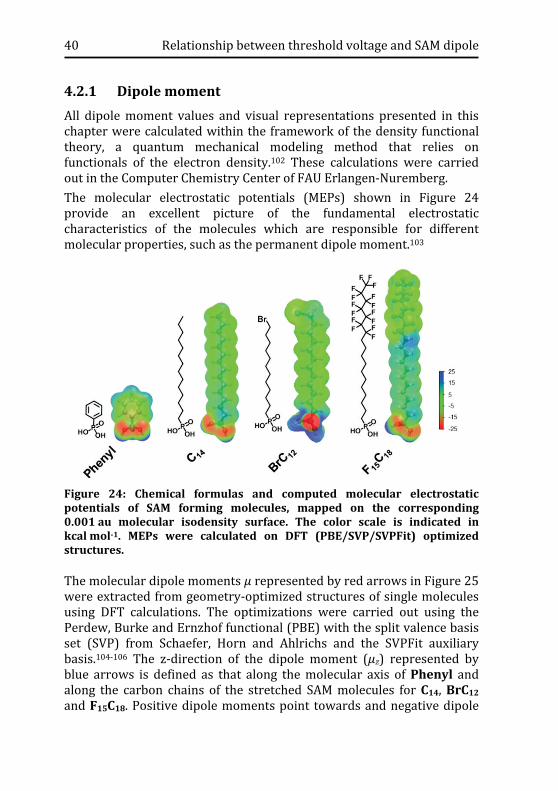
40 Relationship between threshold voltage and SAM dipole
4.2.1 Dipole moment All dipole moment values and visual representations presented in this chapter were calculated within the framework of the density functional theory, a quantum mechanical modeling method that relies on functionals of the electron density.102 These calculations were carried out in the Computer Chemistry Center of FAU Erlangen-Nuremberg. The molecular electrostatic potentials (MEPs) shown in Figure 24 provide an excellent picture of the fundamental electrostatic characteristics of the molecules which are responsible for different molecular properties, such as the permanent dipole moment.103
Figure 24: Chemical formulas and computed molecular electrostatic potentials of SAM forming molecules, mapped on the corresponding 0.001 au molecular isodensity surface. The color scale is indicated in kcal mol-1. MEPs were calculated on DFT (PBE/SVP/SVPFit) optimized structures.
The molecular dipole moments µ represented by red arrows in Figure 25 were extracted from geometry-optimized structures of single molecules using DFT calculations. The optimizations were carried out using the Perdew, Burke and Ernzhof functional (PBE) with the split valence basis set (SVP) from Schaefer, Horn and Ahlrichs and the SVPFit auxiliary basis.104-106 The z-direction of the dipole moment (µz) represented by blue arrows is defined as that along the molecular axis of Phenyl and along the carbon chains of the stretched SAM molecules for C14, BrC12 and F15C18. Positive dipole moments point towards and negative dipole

Relationship between threshold voltage and SAM dipole 41
moments point away from the substrate surface, respectively. The values for µ and µz are listed in Table 1.
Figure 25: The total dipole moments (in red) and the z-component of the dipole moment (in blue) are depicted together with a three-dimensional representation of the SAM molecules. The green reference arrow indicates the value of 1 D. Element color assignment: white for H, grey for C, gold for P, red for O, blue for Br and green for F.
A special case in the calculation of the dipole moments is given for molecule BrC12. Unlike the other molecules, different conformations of BrC12 result in different dipole moments due to the substitution with only one Br-atom (cf. Figure 25). The value listed in Table 1 is the result of a Boltzmann statistics weighting the dipole moment values according to the probability of their conformation (quantified in terms of their energy at room temperature).
Table 1: Total dipole moments µ and their z-components µz.
Molecule Dipole moment µ (D) µz (D) Phenyl 1.234 0.721 C14 1.069 0.274 BrC12 2.106 -0.852 F15C18 2.792 -2.270

42 Relationship between threshold voltage and SAM dipole
4.2.2 Thickness and tilt angle The thickness and the tilt angle of the SAMs were extracted from X-ray reflectivity measurements (XRR) performed on silicon wafers coated with 10 nm aluminum oxide by atomic layer deposition (ALD).
Figure 26: Definition of the tilt angle of a densely packed SAM.
The definition of the tilt angle is shown in Figure 26, so that the following relationship between thickness of the SAM dSAM and length of the molecule lmolecule can be used to determine the tilt angle θ:
The reflected X-ray intensity R was plotted as a function of the wave vector qz. This data served as basis for modeling the electron density of the SAMs as function of the distance from the substrate z. For instance, the electron rich part of molecule F15C18 containing the fluorine atoms can be recognized clearly in the scattering length density profile (SLD) between z = -1 nm and -2 nm, while the alkyl chain of the molecules exhibits a comparably low SLD of roughly 1×10⁻³ nm-2. The effective thickness of each SAM was determined by the half-height method as indicated in Figure 27 with vertical dotted lines in different colors. The line at z = 0 nm corresponds to the substrate surface. The values obtained for the different SAMs are summarized in Table 2. The tilt angles obtained for molecules C14, BrC12 and F15C18 match quite well in the range of values that are expected for alkyl-PA based SAMs between 15° and 30°.39 The XRR measurements for Phenyl could not be reproduced satisfactorily at the ESRF. Thus, the value for the length of Phenyl was taken as substitute for the SAM thickness in this study.
θdSAM
lmolecule
𝒄𝒐𝒔𝜽 =𝒅𝑺𝑨𝑴
𝒍𝒎𝒐𝒍𝒆𝒄𝒖𝒍𝒆 (20)

Relationship between threshold voltage and SAM dipole 43
Figure 27: SLD profiles of the different SAMs on ALD-AlOx and the XRR measurement data depicting the specular reflectivity R(Qz) as a function of the scattering vector qz (circles) and corresponding fit (blue line).
Table 2: Average SAM thickness and tilt angle of the SAMs.
Molecule Length l a) (nm) Thickness dSAM (nm) Tilt angle θ (°) Phenyl 0.57 N/A N/A C14 1.86 1.74 21 BrC12 1.68 1.62 15 F15C18 2.38 2.17 24 a) determined in ChemBioDraw Ultra 13.0
4.2.3 Packing density X-ray photoelectron spectroscopy (XPS) measurements were performed in order to estimate relative packing densities of SAMs. The substrates were silicon wafers covered with 10 nm ALD aluminum oxide. The SAMs were deposited as described in Chapter 3.3. The photoelectron spectra

44 Relationship between threshold voltage and SAM dipole
as a function of kinetic energy were analyzed in the energy range of 0 - 1400 eV (cf. Figure 28).
Figure 28: Photoelectron spectra for the different SAMs and the AlOx reference scanned over the complete energy range.
Figure 29 shows high resolution scans of the aluminum (≈ 75 eV) and phosphorus (≈ 134 - 135 eV) peak for each SAM and the ALD-AlOx sample. The phosphorus signal was taken as a measure for the concentration and packing density of the molecules on the substrate. The intensity of the aluminum signal served for a rough estimation of the attenuation of the signals and was used for correction of the absolute phosphorus signal.
Figure 29: XPS scans for aluminum (a) and phosphorus (b).
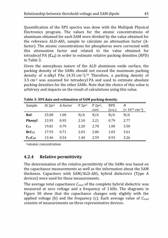
Relationship between threshold voltage and SAM dipole 45
Quantification of the XPS spectra was done with the Multipak Physical Electronics program. The values for the atomic concentrations of aluminum obtained for each SAM were divided by the value obtained for the reference ALD-AlOx sample to calculate an attenuation factor (A-factor). The atomic concentrations for phosphorus were corrected with this attenuation factor and related to the value obtained for tetradecyl PA (C14) in order to estimate relative packing densities (RPD) in Table 3. Given the amorphous nature of the ALD aluminum oxide surface, the packing density of the SAMs should not exceed the maximum packing density of n-alkyl PAs (4.35 cm-2).39 Therefore, a packing density of 3.5 cm-2 was assumed for tetradecyl PA and used to estimate absolute packing densities for the other SAMs. Note that the choice of this value is arbitrary and impacts on the result of calculations using this value.
Table 3: XPS data and estimation of SAM packing density. Sample Al 2pa) A-factor P 2pa) P 2pa),
corr. RPD (a.u.)
N (× 1014 cm-2)
Ref. 25.08 1.00 N/A N/A N/A N/A Phenyl 23.95 0.95 2.10 2.21 0.79 2.77 C14 19.81 0.79 2.20 2.78 1.00 3.50 BrC12 17.93 0.71 2.03 2.86 1.03 3.61 F15C18 13.46 0.54 1.40 2.59 0.93 3.26 a)atomic concentration
4.2.4 Relative permittivity The determination of the relative permittivity of the SAMs was based on the capacitance measurements as well as the information about the SAM thickness. Capacitors with SAM/ALD-AlOx hybrid dielectrics (Type A devices) were used for these measurements. The average total capacitance Ctotal of the complete hybrid dielectric was measured at zero voltage and a frequency of 1 kHz. The diagrams in Figure 30 show that the capacitance changes only slightly with the applied voltage (b) and the frequency (c). Each average value of Ctotal consists of measurements on three representative devices.

46 Relationship between threshold voltage and SAM dipole
Figure 30: Capacitor device layout (a); capacitance Ctotal measured voltage-dependent (b) and frequency-dependent (c).
According to Equation (3), the capacitance of the SAM CSAM can be determined with the knowledge of CAlOx. The capacitance of the AlOx layer was calculated with εAlOx = 7.5, a representative value for aluminum oxide films deposited by atomic layer deposition.107 The relative permittivities for the SAMs were obtained by inserting the values for CSAM and dSAM into Equation (8). Table 4 lists the parameters and values used to calculate the relative permittivity εSAM for samples with an aluminum oxide thickness of 10 nm. The relative permittivities obtained for other AlOx thicknesses are listed in the rows beneath. Molecules Phenyl, C14 and BrC12 exhibit εSAM values between 1.12 and 2.37 without systematic trend for the different AlOx thicknesses. For molecule F15C18 the values are close to 1. The values obtained here are relatively low compared to the representative value of ε = 2.5 reported in the literature for SAMs of n-alkyl silanes and phosphonic acids.16, 108, 109
SAM
ALD-AlOx
Bottom electrode (p-type Si)
Top electrode (Au)
-3 -2 -1 0 1 2 30.1
0.2
0.3
0.4
0.5
0.6
0.7dAlOx = 10 nm
Phenyl C14 BrC12 F15C18
C tota
l (µF
/cm
2 )
Voltage (V)
Frequency = 1 kHz
103 104 105 1060.1
0.2
0.3
0.4
0.5
0.6
0.7
Phenyl C14 BrC12 F15C18
C tota
l (µF
/cm
2 )
Frequency (Hz)
dAlOx = 10 nm Voltage = 0 V
(a)
(b) (c)

Relationship between threshold voltage and SAM dipole 47
Table 4: Relative permittivities εSAM of SAMs.
SAM Phenyl C14 BrC12 F15C18 Ctotal, 10 nm (µF/cm-2) 0.481 0.346 0.351 0.268 CAlOx, 10 nm (µF/cm-2) 0.664 0.664 0.664 0.664 CSAM, 10 nm (µF/cm-2) 1.745 0.722 0.745 0.451 dSAM, 10 nm (nm) 0.57 1.74 1.62 2.17 εSAM, 10 nm (a.u.) 1.12 1.42 1.36 1.10 εSAM, 20 nm (a.u.) 1.43 1.51 1.57 1.09 εSAM, 40 nm (a.u.) 2.26 1.76 1.68 1.04 εSAM, 80 nm (a.u.) 1.71 2.34 2.37 1.13
4.2.5 SAM electrostatic potential Knowledge of the dipole moment, thickness, tilt angle, packing density and relative permittivity for the different SAMs allows for the calculation of the electrostatic potential VSAM according to Equation (13). The average values for 3 devices are listed in Table 5 according to the AlOx dielectric thickness of the samples. The obtained values are in the range between 0.14 V (for C14) and -2.44 V (for F15C18) and agree fairly well with SAM electrostatic potentials reported in literature. A typical value of the electrostatic potential induced by dipole moments of this order of magnitude is around 1 V.66, 82, 85 Fleischli and coworkers reported values between -0.74 V and 0.88 V for SAM molecules with dipole moments between -2.6 D and 3.1 D.85 Kobayashi et al. investigated alkyl- and fluoralkylsilanes with dipole moments of 0.831 D and -2.202 D and their impact on the threshold voltage shifts in OTFTs.82
Table 5: Electrostatic potentials calculated according to Equation (13).
SAM Phenyl C14 BrC12 F15C18 µz (D) 0.721 0.274 -0.852 -2.270 VSAM, 10 nm (V) 0.67 0.24 -0.82 -2.30 VSAM, 20 nm (V) 0.52 0.22 -0.71 -2.33 VSAM, 40 nm (V) 0.33 0.19 -0.66 -2.44 VSAM, 80 nm (V) 0.44 0.14 -0.47 -2.25

48 Relationship between threshold voltage and SAM dipole
4.2.6 SAM surface energy In the frame of this work, the determination of the water static contact angle (SCA) was used to monitor the quality of the SAM, ensuring a reproducible fabrication process. It is known from studies on SAM formation kinetics that the occupancy of the substrate with SAM molecules can be monitored with SCA measurements by analyzing the time needed until saturation of the adsorption curve is observed.23, 24, 110 Deviations of the saturation SCA value can therefore help to identify an error during the processing step of SAM deposition. The SCA values reflect the wettability with the test liquid. Reference surfaces with ALD aluminum oxide treated with oxygen plasma show hydrophilic behavior resulting in SCA values below 10°. Each value in Figure 31 represents the average for five SCA values on the same sample.
Figure 31: Surface energies calculated by Owens & Wendt method (black and red columns) and water contact angles (green squares) obtained for Phenyl, C14, BrC12 and F15C18 SAMs.
C14 and F15C18 exhibit hydrophobic surfaces showing high SCA values (111.5° ± 0.8° for C14 and 122° ± 2.4° for F15C18) and low surface energies (20.93 mN/m for C14 and 8.34 mN/m for F15C18) in the wetting experiments. Similar SCA values were reported for other SAM systems, such as thiols or silanes and with a surface-exposed CH3- or CF3-group, confirming the closely-packed nature of these SAMs.23, 24, 111 Phenyl and BrC12 exhibit lower SCA values (72.6° ± 0.8° for Phenyl and 89.1° ± 1.4° for BrC12) and higher surface energies (41.84 mN/m for Phenyl and
05
1015202530354045505560
Surfa
ce E
nerg
y (m
N/m
)
SE dispersive polar
Phenyl C14 BrC12 F15C18
Molecule
60
70
80
90
100
110
120
130
140 SCA water
SCA (°)

Relationship between threshold voltage and SAM dipole 49
41.16 mN/m for BrC12). These values might indicate either are more disordered surface (probably the case for Phenyl) or a more polar nature of the surface end-groups, which in case of molecule BrC12 could be due to the substitution of just one H-atom with the more electronegative Br-atom.
4.3 Variation of dielectric thickness and impact on capacitor and transistor characteristics
Transistor and capacitor devices of Type A (p-type silicon wafers covered with ALD aluminum oxide as depicted in Figure 16) were used in this series of experiments. Four different aluminum oxide thicknesses (10 nm, 20 nm, 40 nm, 80 nm) were selected to investigate the impact of the dielectric thickness on the turn-on behavior of the transistors. AFM images of all ALD surfaces show a slight increase of the roughness (RMS value) from 0.31 nm for 10 nm AlOx up to 0.39 nm for 80 nm AlOx (cf. Figure 32).
Figure 32: AFM images of different ALD-AlOx surfaces. The RMS values were 0.31 nm for the sample with a 10 nm thick AlOx layer, 0.31 nm for 20 nm AlOx, 0.34 nm for 40 nm AlOx and 0.39 nm for 80 nm AlOx.
All samples were treated with oxygen plasma prior to the deposition of the semiconductor. The evaporation of the semiconductor pentacene was carried out subsequently to the SAM deposition with a constant rate of 0.1 Å/s and a constant substrate temperature of 60 °C. The pentacene layer as well as the gold electrodes had a thickness of 30 nm. Figure 33(a) shows the transfer characteristics of OTFTs with different dielectric thicknesses. It can be observed, that the starting bias was
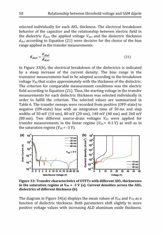
50 Relationship between threshold voltage and SAM dipole
selected individually for each AlOx thickness. The electrical breakdown behavior of the capacitor and the relationship between electric field in the dielectric Ediel, the applied voltage Vdiel and the dielectric thickness ddiel according to Equation (21) were decisive for the choice of the bias range applied in the transfer measurements.
In Figure 33(b), the electrical breakdown of the dielectrics is indicated by a steep increase of the current density. The bias range in the transistor measurements had to be adapted according to the breakdown voltage VBD that scales approximately with the thickness of the dielectric. The criterion for comparable measurement conditions was the electric field according to Equation (21). Thus, the starting voltage in the transfer measurements for each dielectric thickness was selected individually in order to fulfill the criterion. The selected values are summarized in Table 6. The transfer sweeps were recorded from positive (OFF-state) to negative (ON-state) bias with an integration time of 50 ms and step widths of 50 mV (10 nm), 80 mV (20 nm), 140 mV (40 nm) and 260 mV (80 nm). Two different source-drain voltages VDS were applied for transfer measurements in the linear regime (VDS = -0.1 V) as well as in the saturation regime (VDS = -3 V).
Figure 33: Transfer characteristics of OTFTs with different AlOx thicknesses in the saturation regime at VDS = -3 V (a). Current densities across the AlOx dielectrics of different thickness (b).
The diagram in Figure 34(a) displays the mean values of VON and VTH as a function of dielectric thickness. Both parameters shift slightly to more positive voltage values with increasing ALD aluminum oxide thickness.
𝑬𝒅𝒊𝒆𝒍 =𝑽𝒅𝒊𝒆𝒍𝒅𝒅𝒊𝒆𝒍
(21)

Relationship between threshold voltage and SAM dipole 51
VON increases by 13 mV/nm and VTH by 7.6 mV/nm. These shifts could be explained with the increase of trap states in thicker dielectrics and the charge induced by the molecular dipole of OH-groups on the surface of the dielectric. Compared to other dielectrics, the effect on the VTH shift is not very pronounced. Ou-Yang et al. had reported threshold voltage shifts of 180 mV/nm for silicon dioxide dielectrics that were tested in a thickness range between 40 and 500 nm.112 The right diagram in Figure 34(b) displays the measured capacitance of the aluminum oxide dielectric as a function of the aluminum oxide thickness and compares it to the calculated values according to Equation (8). A representative relative permittivity for ALD aluminum oxide of 7.5 was assumed.107 The values calculated for 40 nm and 80 nm thick AlOx are in good agreement with the experimental values. For 20 nm and 10 nm AlOx thickness, a discrepancy can be observed, which could be explained with the charge induced by the OH-groups. The layer of OH-groups can be regarded as a single capacitor connected in series with the aluminum oxide dielectric, altering the capacitance especially in the case of thinner AlOx layers (cf. Chapter 2.3.1). A more detailed investigation of interfacial layers and their impact on the capacitance of ALD AlOx layers can be found in Reference [107].
Figure 34: VTH and VON as a function of the ALD AlOx thickness (a). The measured capacitance as a function of the ALD AlOx thickness is compared to calculated values (b).
Based on the results obtained for the OTFTs and capacitors with unmodified AlOx dielectric (cf. Table 6), the final measurement parameters, especially the bias range for the transfer measurements was determined. The thickness of the ALD aluminum oxide dmeasured was determined by ellipsometry. The capacitance Ci was determined at a frequency of 1 kHz.
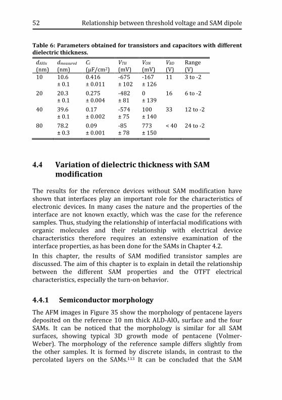
52 Relationship between threshold voltage and SAM dipole
Table 6: Parameters obtained for transistors and capacitors with different dielectric thickness.
dAlOx (nm)
dmeasured (nm)
Ci (µF/cm2)
VTH (mV)
VON (mV)
VBD (V)
Range (V)
10 10.6 ± 0.1
0.416 ± 0.011
-675 ± 102
-167 ± 126
11 3 to -2
20 20.3 ± 0.1
0.275 ± 0.004
-482 ± 81
0 ± 139
16 6 to -2
40 39.6 ± 0.1
0.17 ± 0.002
-574 ± 75
100 ± 140
33 12 to -2
80 78.2 ± 0.3
0.09 ± 0.001
-85 ± 78
773 ± 150
< 40 24 to -2
4.4 Variation of dielectric thickness with SAM modification
The results for the reference devices without SAM modification have shown that interfaces play an important role for the characteristics of electronic devices. In many cases the nature and the properties of the interface are not known exactly, which was the case for the reference samples. Thus, studying the relationship of interfacial modifications with organic molecules and their relationship with electrical device characteristics therefore requires an extensive examination of the interface properties, as has been done for the SAMs in Chapter 4.2. In this chapter, the results of SAM modified transistor samples are discussed. The aim of this chapter is to explain in detail the relationship between the different SAM properties and the OTFT electrical characteristics, especially the turn-on behavior.
4.4.1 Semiconductor morphology The AFM images in Figure 35 show the morphology of pentacene layers deposited on the reference 10 nm thick ALD-AlOx surface and the four SAMs. It can be noticed that the morphology is similar for all SAM surfaces, showing typical 3D growth mode of pentacene (Volmer-Weber). The morphology of the reference sample differs slightly from the other samples. It is formed by discrete islands, in contrast to the percolated layers on the SAMs.113 It can be concluded that the SAM
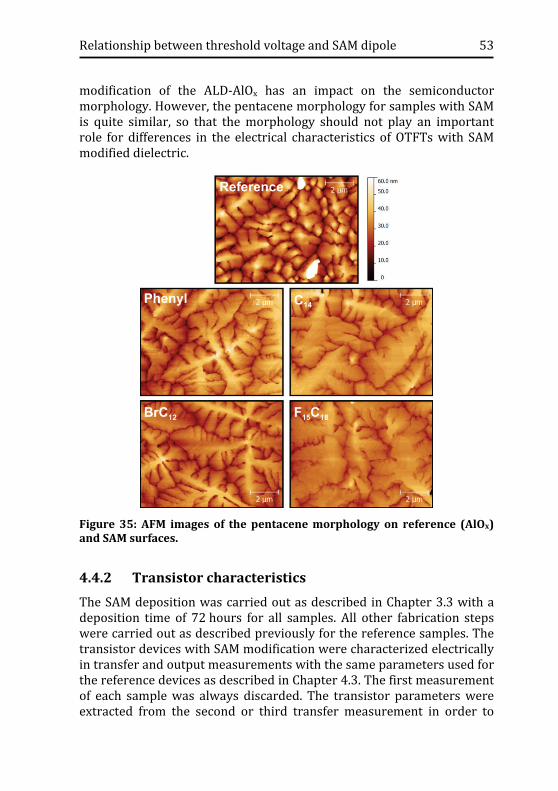
Relationship between threshold voltage and SAM dipole 53
modification of the ALD-AlOx has an impact on the semiconductor morphology. However, the pentacene morphology for samples with SAM is quite similar, so that the morphology should not play an important role for differences in the electrical characteristics of OTFTs with SAM modified dielectric.
Figure 35: AFM images of the pentacene morphology on reference (AlOx) and SAM surfaces.
4.4.2 Transistor characteristics The SAM deposition was carried out as described in Chapter 3.3 with a deposition time of 72 hours for all samples. All other fabrication steps were carried out as described previously for the reference samples. The transistor devices with SAM modification were characterized electrically in transfer and output measurements with the same parameters used for the reference devices as described in Chapter 4.3. The first measurement of each sample was always discarded. The transistor parameters were extracted from the second or third transfer measurement in order to

54 Relationship between threshold voltage and SAM dipole
avoid a possible impact of the bias stress effect on the device characteristics.114 Figure 36 shows representative transfer characteristics for all samples tested in this series. None of the samples showed a pronounced hysteresis (< 50 mV) in the transfer characteristic (the backward measurement from ON to OFF-state is not shown in Figure 36). Each diagram displays the characteristics obtained for the respective thickness of the ALD-AlOx dielectric indicated in the lower left corner of each diagram.
Figure 36: Transfer characteristics for different SAMs and for different ALD-AlOx thicknesses: 10 nm (a), 20 nm (b), 40 nm (c) and 80 nm (d).
The characteristics of samples modified with SAMs of molecule F15C18 (µz = -2.27 D) exhibit the largest VTH shift from 1083 mV for 10 nm AlOx to 13908 mV for 80 nm AlOx. Samples with BrC12 (µz = -0.85 D) exhibit a VTH range between -563 mV for 10 nm AlOx and 2047 mV for 80 nm AlOx. Compared to F15C18 the VTH shift with increasing AlOx thickness is thus not that pronounced for BrC12. For the reference sample only a slight shift to positive bias can be observed, as previously described in Chapter 4.3. For Phenyl (µz = 0.72 D) and C14 (µz = 0.27 D) the shifts of VTH were even less pronounced as for the reference samples. They

Relationship between threshold voltage and SAM dipole 55
remained nearly constant for all AlOx thicknesses. The same applied for the VON values. All VTH and VON values are summarized in Table 7 and Table 8.
Table 7: Average threshold voltage VTH in mV.
dAlOx (nm) Ref. Pheny
C14 BrC12 F15C18 10 -675
± 102 -1007 ± 16
-720 ± 15
-563 ± 18
1083 ± 15
20 -482 ± 81
-878 ± 69
-486 ± 118
23 ± 63
3041 ± 132
40 -574 ± 75
-1084 ± 99
-458 ± 247
880 ± 93
6429 ± 299
80 -85 ± 78
-818 ± 120
-667 ± 116
2047 ± 66
1390 ± 394
Table 8: Average turn-on voltage VON in mV.
dAlOx (nm) Ref. Pheny
C14 BrC12 F15C18 10 -167
± 126 -417 ± 58
-267 ± 29
117 ± 29
2100 ± 10
20 0 ± 139
-427 ± 46
-53 ± 122
747 ± 92
4293 ± 122
40 100 ± 140
-693 ± 81
147 ± 323
2200 ± 370
8127 ± 450
80 773 ± 150
513 ± 150
167 ± 150
3720 ± 260
15767 ± 397
The saturation charge carrier mobilities µsat were determined as described in Chapter 2.3.2. Samples with dielectrics modified with C14 and F15C18 exhibit the highest mobility values with a maximum average mobility of 0.867 cm2/Vs for F15C18 on 40 nm AlOx and 0.779 cm2/Vs for C14 on 40 nm AlOx. The surfaces with a high surface energy (C14 and F15C18) result in a favorable orientation of pentacene molecules at the first monolayer on the SAM which result in good charge transport properties. In contrast, Phenyl and BrC12 exhibit lower mobilities compared to the reference (µsat = 0.165 cm2/Vs for dAlOx = 40 nm). This can be explained with the disturbed (Phenyl) or more polar surface (BrC12) provided by these molecules, as described in Chapter 4.2.6. All µsat values are summarized in Table 9. These do not reveal a consistent relationship between charge carrier mobility and thickness of AlOx.

56 Relationship between threshold voltage and SAM dipole
For the subthreshold swing S, however, a clear increase with increasing AlOx thickness is observed for all samples (cf. Table 10). This indicates an increase of the interfacial trap state density probably due to an increased roughness at thicker AlOx layers (cf. Figure 32).
Table 9: Average charge carrier mobilities µsat in cm2/Vs.
dAlOx (nm) Ref. Phenyl C14 BrC12 F15C18 10 0.134
± 0.014 0.072 ± 0.003
0.769 ± 0.011
0.241 ± 0.011
0.681 ± 0.040
20 0.157 ± 0.002
0.036 ± 0.001
0.594 ± 0.045
0.333 ± 0.022
0.352 ± 0.009
40 0.165 ± 0.013
0.040 ± 0.002
0.779 ± 0.035
0.327 ± 0.007
0.867 ± 0.043
80 0.150 ± 0.033
0.027 ± 0.003
0.447 ± 0.071
0.185 ± 0.039
0.316 ± 0.027
Table 10: Average subthreshold swing S in mV/dec. dAlOx (nm) Ref. Phenyl C14 BrC12 F15C18 10 97 ± 3 135 ± 1 98 ± 5 114 ± 1 101 ± 5 20 131 ± 2 181 ± 3 124 ± 5 164 ± 5 197 ± 2 40 211 ± 3 174 ± 2 150 ± 5 193 ± 1 245 ± 6 80 334 ± 6 347 ± 2 277 ± 8 301 ± 4 369 ± 6
The diagrams in Figure 37 clarify the dependency of VON and VTH from the AlOx thickness. The SAMs exhibiting negative electrostatic potentials (BrC12 and F15C18) show the largest shifts of the transfer characteristic and exceed the shifts observed for the reference samples. The reference samples exhibit a small shift of 7.6 mV/nm and 13.0 mV/nm for VTH and VON, respectively. For F15C18, the shifts amount to 184 mV/nm (VTH) and 200 mV/nm (VON). As all other components of the transistor devices were fabricated under identical conditions, the larger shifts of VTH and VON compared to the reference have to be related to the SAM. In the next chapter an attempt to explain the effect of the SAM electrostatic potential on the turn-on behavior of OTFTs will be presented.
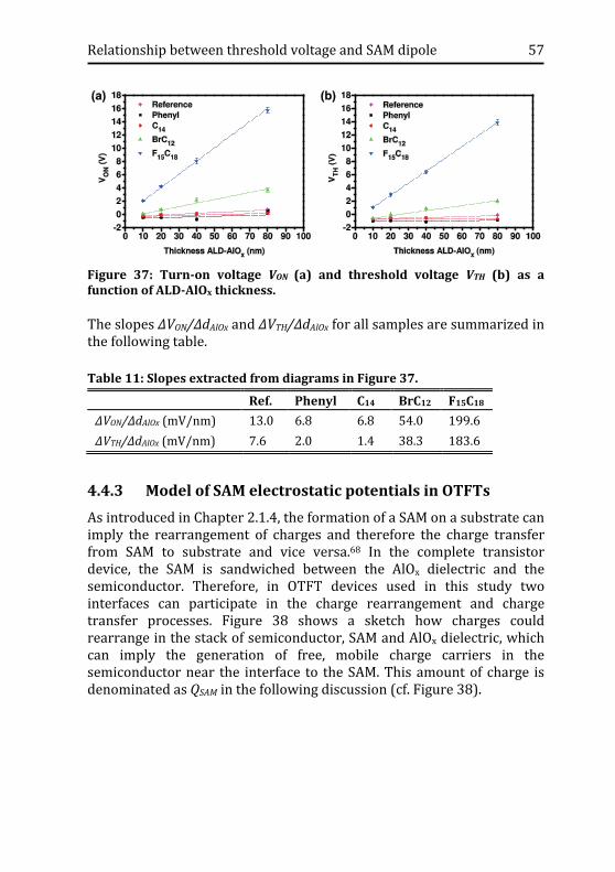
Relationship between threshold voltage and SAM dipole 57
Figure 37: Turn-on voltage VON (a) and threshold voltage VTH (b) as a function of ALD-AlOx thickness.
The slopes ΔVON/ΔdAlOx and ΔVTH/ΔdAlOx for all samples are summarized in the following table.
Table 11: Slopes extracted from diagrams in Figure 37.
Ref. Phenyl C14 BrC12 F15C18 ΔVON/ΔdAlOx (mV/nm) 13.0 6.8 6.8 54.0 199.6 ΔVTH/ΔdAlOx (mV/nm) 7.6 2.0 1.4 38.3 183.6
4.4.3 Model of SAM electrostatic potentials in OTFTs As introduced in Chapter 2.1.4, the formation of a SAM on a substrate can imply the rearrangement of charges and therefore the charge transfer from SAM to substrate and vice versa.68 In the complete transistor device, the SAM is sandwiched between the AlOx dielectric and the semiconductor. Therefore, in OTFT devices used in this study two interfaces can participate in the charge rearrangement and charge transfer processes. Figure 38 shows a sketch how charges could rearrange in the stack of semiconductor, SAM and AlOx dielectric, which can imply the generation of free, mobile charge carriers in the semiconductor near the interface to the SAM. This amount of charge is denominated as QSAM in the following discussion (cf. Figure 38).

58 Relationship between threshold voltage and SAM dipole
Figure 38: Schematic of charge rearrangement in the proximity of the SAM. The negative dipole moment perpendicular to the surface of the SAM induces mobile holes in semiconductor (QSAM).
If an external potential VGS is applied between gate and source electrodes of a transistor device (cf. Figure 39), the effective amount of charge carriers Qeff accumulated in the semiconductor in the vicinity of the interface to the dielectric is proportional to the effective voltage at this interface and the total capacitance of the dielectric Ctotal:
The dielectric of the transistor in Figure 39 has a hybrid dielectric composed of AlOx and a SAM. The capacitance of the semiconductor CSC is neglected in this case because only the charges that are generated directly at the semiconductor/dielectric interface are considered. Thus, the total capacitance of the dielectric can be calculated by:
Figure 39: Effect of the electrostatic potential in the OTFT device. Additional mobile holes are induced in the semiconductor.
QSAM
µz µz
Source Drain
Substrate
Gate
AlOx
CSAM
CAlOx
CSC
𝑸𝒆𝒇𝒇 = 𝑽𝑮𝑺,𝒆𝒇𝒇 ∙ 𝑪𝒕𝒐𝒕𝒂𝒍 (22)
𝑪𝒕𝒐𝒕𝒂𝒍 = 𝟏
𝑪𝑨𝒍𝑶𝒙+
𝟏𝑪𝑺𝑨𝑴
−𝟏
(23)

Relationship between threshold voltage and SAM dipole 59
Mobile charges that are induced by the SAM due to its electrostatic potential add up to the charges accumulated at the interface of semiconductor and dielectric. Thus, the potential between source and drain electrode screens this additional charges and is shifted accordingly. It is assumed that the shift is approximately proportional to the amount of charges induced by the SAM (QSAM). Therefore, it can be written:
The amount of charges can be approximated by the following relationship:
It is assumed that during operation of the transistor the potential drop across the SAM is equivalent to VSAM and that ΔVGS,eff is identical to the shift of the threshold voltage ΔVTH or the turn-on voltage ΔVON. Finally, by inserting Equation (25) into Equation (24), a relationship that describes the effect of the SAM electrostatic potential on the shift of the OTFT characteristic quantitatively is proposed:
The sign for the change of threshold voltage ΔVTH and turn-on voltage ΔVON results from the definition that was made for the direction of the dipole moment (a negative dipole moment leads to accumulation of holes and a shift to positive bias and vice versa). A similar relationship has been used by Huang and coworkers to explain the threshold voltage or turn-on voltage shifts in SAM-modified OTFTs.115 However, the agreement between experimental and calculated data was quite poor in this study. The next two Figures (Figure 40 and Figure 41) compare experimental data for VON and VTH with values calculated by Equation (26). The values for VSAM were taken from Table 5 and therefore differ for each AlOx thickness. Note that it is not possible to predict absolute values of VON and VTH with Equation (26), since further contributions (e.g. the flat-band potential) are either not known or simply neglected in this calculation (cf. Chapter 2.3.3). However, as the reference samples without SAM
∆𝑽𝑮𝑺,𝒆𝒇𝒇 =𝑸𝑺𝑨𝑴
𝑪𝒕𝒐𝒕𝒂𝒍 (24)
𝑸𝑺𝑨𝑴 = 𝑪𝑺𝑨𝑴 ∙ 𝑽𝑺𝑨𝑴 (25)
∆𝑽𝑮𝑺,𝒆𝒇𝒇 = 𝑽𝑺𝑨𝑴 ∙ 𝑪𝑺𝑨𝑴𝑪𝒕𝒐𝒕𝒂𝒍
= −∆𝑽𝑻𝑯 = −∆𝑽𝑶𝑵 (26)

60 Relationship between threshold voltage and SAM dipole
exhibit VON and VTH values in the range of 0 ± 1 V (cf. Table 7 and Table 8) a comparison between calculated shifts and measured values can be justified. In general, it can be stated that the calculated values agree better with measured VON values than with VTH values. According to Pernstich et al., the threshold voltage VTH is tied to the turn-on voltage VON via the trap density.83 This explains why the calculated values have a better agreement with VON, since the threshold voltage includes the contribution of the trap density. Additionally, it is assumed that the trap density increases with increasing AlOx thickness (due to increasing subthreshold swing S), so that the difference between VON and VTH also depends on the dielectric thickness.
Figure 40: Comparison of experimental values for VON with values calculated by Equation (26) for ALD-AlOx thickness of 10 nm (a), 20 nm (b), 40 nm (c) and 80 nm (d).
The plotted values in the VON vs. VSAM diagram in Figure 40 reveal that the calculated values agree quite well with the measured ones for F15C18. For BrC12 the prediction by Equation (26) is also quite fair for 10 nm and 20 nm AlOx thickness. For 40 nm and 80 nm AlOx thickness, the calculated values are much larger than the measured VON values. In case

Relationship between threshold voltage and SAM dipole 61
of Phenyl and C14, the prediction by Equation (26) is also quite accurate for 10 nm AlOx. But with increasing thickness of AlOx, the discrepancy between measured and predicted values gets larger, especially for molecule Phenyl. The same observations apply for the plot of VTH vs. VSAM (cf. Figure 41). The diagrams in Figure 42 and Figure 43 show the difference between the theoretical values predicted by Equation (26) and the experimental values for VON and VTH and illustrate more clearly the results of Figure 40 and Figure 41.
Figure 41: Comparison of experimental values for VTH with values calculated by Equation (26) for ALD-AlOx thickness of 10 nm (a), 20 nm (b), 40 nm (c) and 80 nm (d).

62 Relationship between threshold voltage and SAM dipole
Figure 42: Difference between values predicted by Equation (26) and experimental values for VON.
Figure 43: Difference between values predicted by Equation (26) and experimental values for VTH.
Relationship between threshold voltage and SAM dipole 63
In summary, it can be observed that Equation (26) provides a quite accurate prediction of VON for F15C18. It overestimates VON for C14 and BrC12, and for molecule Phenyl the prediction fails completely for thicker AlOx. An attempt to explain these observations will be presented in the following discussion. In Figure 44, the band diagrams show the stack of gate electrode, AlOx dielectric and pentacene. In (a) an ideal MIS capacitor under flat-band conditions is shown. Applying a potential VG < VTH leads to accumulation of holes in the semiconductor near the interface to the AlOx dielectric (b). In the band diagrams below, the two cases of negative and positive dipole moments µz are considered. In (c) and (d) the negative dipole moment µz of the SAM molecules induces additional holes under flat-band condition and under negative bias, respectively. A SAM with a positive dipole moment µz leads to an increase of the electron density in the semiconductor in the proximity to the SAM (e). The negative gate potential compensates the additional electrons at the interface (f). Further increase of the potential would lead to accumulation of holes as in (b) and (d). The electrostatic potential of the SAM (VSAM) has the same effect as an external potential VG on the band bending of HOMO and LUMO in this simple model. Also, it was shown that the shifts of VTH and VON can be predicted quite accurately with Equation (26) for some SAMs. But it must be clarified if the equation has a general character and if it is able to describe VTH and VON shifts for different cases, e.g. positive and negative electrostatic potentials and p-type and n-type semiconductors. As observed for Phenyl in Figure 40 and Figure 41, the prediction of ΔVTH or ΔVON with Equation (26) does not result in a good agreement for thicker AlOx. Of course this could be due to an erroneous estimation of the electrostatic potential. But the failure of the application of Equation (26) could also be related to the nature of the semiconductor.

64 Relationship between threshold voltage and SAM dipole
Figure 44: Band diagrams of MIS structures showing different cases of dielectric modification: No SAM modification of the dielectric ((a) and (b)), SAM with negative µz ((c) and (d)) and SAM with positive µz ((e) and (f)). The left diagrams show the MIS structure under flat-band conditions. The right diagrams show the MIS structure under negative bias at the gate electrode.
It is known that in OTFTs there is normally no formation of inversion layers, i.e. the formation of a layer conformed by minority charge carriers.116, 117 This means that unlike for holes, there is no screening of
Gate AlOx Pentacene
LUMO
HOMOEf
SAM
V <VG TH
(a) (b)
(c) (d)
(e) (f)
Ener
gy

Relationship between threshold voltage and SAM dipole 65
electrons by the electric field between source and gate. As a result, Equation (26) fails to predict shifts of VTH and VON. On the other hand, it was observed that the VTH and VON values for molecules with positive dipole moment (Phenyl and C14) are shifted to more negative values compared to the reference (cf. values in Table 7 and Table 8). This would agree with the direction of the shift predicted by Equation (26). The magnitude of the VTH and VON shifts is in the range of the electrostatic potential VSAM for the two molecules (VSAM (Phenyl) = 0.33 V – 0.67 V and VSAM (C14) = 0.14 – 0.24 V). These observations lead to the conclusion that Equation (26) applies only when the electrostatic potential of the SAMs results in a generation of mobile charge carriers that can be screened by the external field. It is assumed that the SAM electrostatic potential induces a polarization of the semiconductor molecules near the interface to the SAM. This polarization leads to a change of the charge carrier density.81 The generation of mobile charge carriers relies on the external injection and constant supply of the charge carriers from the electrodes. However, the work-function difference of pentacene and the gold electrodes is too large to enable electron injection into the semiconductor.117 Therefore, only a static shift of VTH and VON due to the change of the charge carrier density in the semiconductor is obtained. This static shift should be equal to VSAM if it is assumed that no inversion layer is formed. The next aspect that has to be clarified is the validity of the model for n-type semiconductors. According to the model, in the case of n-type semiconductors, SAMs with a negative electrostatic potential should lead to a static shift (equal to VSAM) of VTH and VON to more positive bias. An additional accumulation of electrons and a shift of the transfer characteristic to more negative bias is expected for SAMs with positive VSAM. The original aim was to conduct the same series of transistor devices with the n-type semiconductor Buckminster Fullerene (C60). Unfortunately, it was not possible to fabricate working devices with this material under the same fabrication conditions that were applied in the case of pentacene transistors. The AFM images in Figure 45 show that the semiconductor layer evaporated onto the ALD-AlOx/SAM substrates is not covering the whole area. Thus, the morphology of the semiconductor could be a reason for the nonfunctional devices.

66 Relationship between threshold voltage and SAM dipole
Figure 45: AFM images of C60 deposited on different SAMs.
4.5 Quantitative analysis of threshold voltage for p- and n-type semiconductors
The study in this chapter has been published in Reference [118] (Copyright © 2012, American Chemical Society). The results for a series of transistors (and capacitors) based on device layout Type B (Figure 18 in Chapter 3.1.1) will be presented in the following. In this series the range of tested materials was extended to six SAM molecules and three semiconductors: pentacene, α,ω-dihexyl-sexithiophene (DH6T) and C60. Devices with C60 were fabricated with aluminum source and drain (or top) electrodes in order to reduce contact resistance by better matching of the work functions (C60: 3.7 eV, Al: 4.2 eV) compared to gold electrodes (Au: 5.1 eV).70, 119
Figure 46: AFM image of an oxygen plasma-oxidized aluminum oxide surface.

Relationship between threshold voltage and SAM dipole 67
In contrast to layout A with unpatterned p-type Si gate electrode and ALD-AlOx dielectric, the devices with layout B consisted of an ultra-thin AlOx dielectric that was generated through an oxygen plasma treatment of the patterned aluminum gate (or bottom) electrode. These films exhibit an increased roughness (RMSPlasma-AlOx ≈ 1.32 nm @ 0.5 µm2) compared to ALD films (RMSALD-AlOx ≈ 0.3 – 0.4 nm @ 0.5 µm2). The morphology of the semiconductors on top of the dielectrics of layout B is shown exemplarily in Figure 47 for SAM molecules C14 and F15C18. Pentacene exhibits a discrete island growth on both SAM molecules, similar to the growth mode observed for the ALD-AlOx reference sample (cf. Figure 35). Percolated layer growth might be inhibited by the larger surface roughness of the plasma-oxidized AlOx layers that offer more nucleation sites than the ALD layer. The morphology of C60 on C14 and F15C18 SAMs on plasma-oxidized AlOx exhibited similar morphologies as observed on ALD-AlOx layers with pronounced gaps between the single grains. In contrast to the ALD-AlOx samples, devices based on plasma-oxidized AlOx yielded functional devices.
Figure 47: Morphology of DH6T, pentacene and C60 on SAMs of molecules C14 (upper row) and F15C18 (lower row), respectively. The layer of 30 nm pentacene on molecule F15C18 exhibits large gaps in comparison to all other combinations of SAMs and semiconductors. Adapted with permission from Reference [118]. Copyright © 2012, American Chemical Society.

68 Relationship between threshold voltage and SAM dipole
All molecules used in this series are summarized in Figure 48 and are arranged according to their dipole moment µz. Compared to the series based on transistor devices with layout A, the amount of molecules was extended to six molecules, with BrC12 being substituted by 4T-C12, BTBT-C12 and C60-C18 in order to have a broader range of µz values.
Figure 48: The total dipole moments (in red) and the z-component of the dipole moment (in blue) are depicted together with a three-dimensional representation of the SAM molecules. The green reference arrow indicates the value of 1 D. Adapted with permission from Reference [118]. Copyright © 2012, American Chemical Society.
The capacitance was measured on samples with gold top electrodes (Al/AlOx-SAM/Au) at a frequency of 100 kHz. The electrical characterization of the transistors was done in the glove box under nitrogen atmosphere. All transfer scans were measured with an integration time of 50 ms, steps of 40 mV, 2 s hold time and swept from positive to negative bias for p-type semiconductors and vice versa for C60. The transistor parameters VTH and µsat were determined by plotting the square root of the saturation current vs. source-gate voltage. Additionally, a backward threshold voltage (VTH, back) was determined from the backward scan for SAMs that exhibit a notable hysteresis in the transfer scan analogously to VTH in the forward scan. For such samples, the threshold voltage depends strongly on the starting bias applied in the transfer scan because of varying numbers of trapped charges induced by different biases. In order to rule out any effect of the measuring
Ref
eren
ce µ
z(1
D)

Relationship between threshold voltage and SAM dipole 69
conditions on the threshold voltage, the starting bias was kept constant in the transfer measurements for each semiconductor (1 V for the p-type SCs and −0.5 V for C60). The first measurement of each sample was always discarded and only fresh samples were used to avoid the known bias stress effect on the threshold voltage.
Figure 49: Representative transfer characteristics for OTFTs with DH6T and C60 and different SAMs. Adapted with permission from Reference [118]. Copyright © 2012, American Chemical Society.
The charge carrier mobilities ranged from 0.009 - 0.034 cm2/Vs for DH6T, 0.001 - 0.833 cm2/Vs for pentacene and 0.004 - 0.164 cm2/Vs for C60. Independently of the semiconductor, a pronounced shift of VTH from negative to more positive values with increasing dipole moment of the SAM molecules could be observed (Figure 49). The average values of VTH for all SAMs and all semiconductors are listed in Table 12. Each value consists of measurements on at least four representative devices. Large values for hysteresis (> 50 mV) were obtained for samples with SAMs of molecules 4T-C12 and C60-C18, therefore the values for VTH, back for these two molecules are indicated in Table 12. Although the results in Chapter 4.4 revealed that the predicted values calculated with the electrostatic potential VSAM were in better agreement with the turn-on voltage VON, the following discussion of the results is constrained to the values obtained for the threshold voltage VTH, because for some of the samples VON could not be determined accurately due to high leakage currents. Another drawback compared to the series of
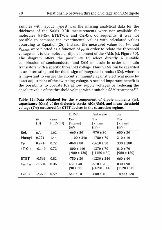
70 Relationship between threshold voltage and SAM dipole
samples with layout Type A was the missing analytical data for the thickness of the SAMs. XRR measurements were not available for molecules 4T-C12, BTBT-C12 and C60-C18. Consequently, it was not possible to compare the experimental values with calculated values according to Equation (26). Instead, the measured values for VTH and VTH,back were plotted as a function of μz in order to relate the threshold voltage shift to the molecular dipole moment of the SAMs (cf. Figure 50). The diagram offers the possibility to select directly a suitable combination of semiconductor and SAM molecule in order to obtain transistors with a specific threshold voltage. Thus, SAMs can be regarded as an interesting tool for the design of integrated circuits (ICs), where it is important to ensure the circuit´s immunity against electrical noise by exact adjustment of the switching voltage. A second important benefit is the possibility to operate ICs at low supply voltages by reducing the absolute value of the threshold voltage with a suitable SAM treatment.120
Table 12: Data obtained for the z-component of dipole moments (μz), capacitance (Ctotal) of the dielectric stacks AlOx/SAM, and mean threshold voltage (VTH) measured for OTFT devices in the saturation regime.
DH6T Pentacene C60
μz (D)
Ctotal
(µF/cm2) VTH
[VTH,back]
(mV)
VTH
[VTH,back]
(mV)
VTH
[VTH,back]
(mV)
Ref. n/a 1.62 -660 ± 50 -970 ± 30 600 ± 30 Phenyl 0.721 1.44 -1100 ± 240 -1780 ± 70 310 ± 10 C14 0.274 0.72 -860 ± 80 -1610 ± 50 330 ± 180 4T-C12 -0.149 0.72 -800 ± 140
[-900 ± 120] -1370 ± 70 [-1460 ± 30]
810 ± 70 [980 ± 150]
BTBT -0.561 0.82 -750 ± 20 -1230 ± 240 660 ± 40 C60-C18 -1.584 0.86 450 ± 40
[90 ± 30] -510 ± 70 [-1090 ± 140]
830 ± 90 [1120 ± 20]
F15C18 -2.270 0.59 640 ± 10 -600 ± 40 1890 ± 120

Relationship between threshold voltage and SAM dipole 71
Figure 50: Mean values for VTH plotted as a function of µz for different semiconductors. The solid black line indicates the theoretical correlation described by Equation (13). Data for C60 is marked in blue, for DH6T in red and for pentacene in green. Adapted with permission from Reference [118]. Copyright © 2012, American Chemical Society.
The black solid line in Figure 50 indicates the theoretical correlation between the electrostatic potential induced by the SAM dipole VSAM and the dipole moment along the molecular axis (μz), according to Equation (13). For the packing density N a value of 3.5 x 1014 cm-2 was selected, assuming densely packed SAMs of all molecules. This value corresponds to the packing density of C14, assumed in Chapter 4.2.3 for the evaluation of the XPS measurements. Comparable values for N are expected for molecules 4T-C12 and BTBT-C12, where the packing densities should be dictated by the footprint of the phosphonic acid anchor group. In the case of C60-C18, a reduced packing density is expected because of the large C60 head group with a diameter of roughly 1 nm.121 For Phenyl, the XPS measurements indicated a reduced packing density of 2.77 x 1014 cm-2. A representative value of 20° was assumed for the tilt angle θ, based on the results of the XRR measurements (cf. Chapter 4.2.2). The results in Chapter 4.2.4 for capacitors based on device layout Type A gave relative permittivities between 1.12 and 2.37 for the different SAMs. These values were slightly lower than the value of ε = 2.5 reported in the literature for SAMs of n-alkyl silanes and phosphonic acids.16, 108, 109
-2.5 -2.0 -1.5 -1.0 -0.5 0 0.5 1.0-2500-2000-1500-1000-500
0500
1000150020002500
C60-C18 F15C18 4T-C12 (back) C60-C18 (back)
VSAM - 700 mV VSAM - 1500 mV VSAM + 500 mV
Phenyl C14 4T-C12 BTBT-C12
VSAM(µz) V
TH (m
V)
µz (D)
72 Relationship between threshold voltage and SAM dipole
A representative value of εSAM = 2 was chosen for the correlation shown in Figure 50. The choice of this value is arbitrary and has an impact on the slope of the black solid line. The theoretical description of VSAM(µz) can be shifted vertically along the ordinate to match the data points for C14, indicated in dashed lines and different colors for each semiconductor. The trend suggested by the correlation between VSAM and µz is supported fairly well by the data obtained for the other SAM molecules, as predicted by Equation (13). According to Equation (26), the threshold voltage shift ΔVTH is described by the product of the electrostatic potential VSAM and the quotient of CSAM/Ctotal. The fair agreement of measured values and theoretical values for VSAM (cf. Figure 50) suggests that the quotient CSAM/Ctotal has to be close to unity in order to satisfy Equation (26). An estimation of CSAM/Ctotal for C14 confirms the correlation. The total capacitance Ctotal measured for the stack of AlOx/C14 is 0.72 µF/cm2. The theoretical capacitance CSAM of a C14 SAM is approximately 1.0 µF/cm2 for εSAM = 2 and a SAM thickness of 1.74 nm (cf. with value for C14 in Table 2). All molecules in this study exhibit values of Ctotal and CSAM in a similar range as for molecule C14. Therefore, the quotient CSAM/Ctotal should be in the range of unity for all molecules, which supports the relationship predicted by Equation (26). The quotient CSAM/Ctotal becomes quite large for thicker dielectrics modified with SAMs due to the lower capacitance of the entire dielectric Ctotal. This was the case for the samples with thicker ALD-AlOx in Chapter 4.4. Similar observations are found in the literature. For SiO2 dielectrics with a thickness of several hundred nanometers, the potential shifts induced by silane SAMs can be enhanced considerably, leading to large VTH shifts in the range of several tens of volts.82, 83 Space charge layers, residual charge carriers or trapped charges in the dielectric, introduced by charge transfer between the SAM or dielectric defects and the semiconductor, are often discussed as the most probable effects that affect the threshold voltage of SAM-modified transistors, as described by Possanner et al., Fleischli et al. and Gholamrezaie et al., respectively.84-86 However, the fair agreement between the experimental data and the theoretical expectations suggest that these effects do not play a major role in the devices investigated in this study. The shifts from the black solid line for the different semiconductors (Figure 50) may allow an estimation of additional contributions to the threshold voltage, such as the flat-band potential, which accounts for any work-function difference between semiconductor and the gate electrode.

Relationship between threshold voltage and SAM dipole 73
For this purpose, calculated work functions for the three semiconductors were related to the deviations from the theoretical correlation given by Equation (13). The work function WF of the semiconductors was estimated by:
with 𝜒 as the electron affinity and Eg as the electronic band gap. To estimate the work-functions of the different organic semiconductors, the band gaps were calculated from the lowest-energy excited states using the semiempirical UNO-CIS method using the AM1 Hamiltonian. Vertical and adiabatic electron affinities were calculated using different ab initio and DFT methods on geometries optimized at the PBEPBE/SVP/SVPFit level of theory. Details about the calculations can be found in the supporting information of Reference [118]. The values obtained for the work functions (pentacene = 1.73 eV, DH6T = 2.08 eV, C60 = 3.29 eV) scale qualitatively with the order of the shifts (pentacene = -1500 mV, DH6T = -700 mV, C60 = 500 mV), and therefore support the assignment of the contribution of the flat-band potential to the measured threshold voltages. Further contributions to the charge accumulation, and consequently to the measured threshold voltage, can originate from interfacial traps. An ohmic drop through the semiconductor and polarization of the organic semiconductor at the metal electrodes can also play an important role for the charge injection into the organic semiconductor and can therefore impact VTH.122, 123 Thus, the dipole effect cannot be defined exactly as several additional effects related to the properties of the SAM molecules and the SAM morphology also contribute to the absolute values of VTH. Charge trapping affects the threshold voltage, as has been extensively reviewed by Dhar et al.123 If charge trapping is involved, it is difficult to relate the measured values for VTH with the properties of the dielectric layer unless the number of trapped charges is known. The absolute VTH values have to be further corrected for fixed oxide charges.
𝑾𝑭 = 𝝌 + 𝑬𝒈𝟐 (27)
74 Relationship between threshold voltage and SAM dipole
4.6 Redox-active SAM molecules and their impact on hysteresis
In the previous chapters, the influence of permanent molecular dipoles on the turn-on characteristics of OTFTs with SAM-modified hybrid dielectrics was discussed. The effect relies on the additional electrostatic field of the dipolar SAM-molecules which reduces or enhances the applied gate field. It has been shown that by varying the stoichiometric composition of SAMs that consist of mixtures of molecules with different dipoles a continuous control of VTH (or VON) in p- and n-type OTFTs can be realized.120, 124 However, in many cases the VTH shift caused by SAM dipoles is overlaid with other changes in the device characteristics. For instance, the appearance and nature of hysteresis during operation are typically attributed to the dielectric layer, whereas variations of the charge-carrier mobility are associated with the semiconductor and changes in its arrangement on the dielectric surface (grain size, orientation etc.).83, 125 Thus, molecular rearrangements or charging of the dielectrics are reasonable causes for hysteresis. Charging in particular leads to a change of the dielectric permittivity and thus to a shift in VTH, as used exquisitely in floating-gate memory transistors.126, 127 The large variety of molecules that form SAMs allows ones that have approximately equal dipole moments, but different abilities to attract and trap charges to be synthesized. Using such molecular dielectrics in operating devices helps distinguish between the effects of molecular dipoles and the ability to trap charge on VTH-shift and hysteresis. In order to explore this approach, a series of thin-film transistor devices using pure and mixed SAMs of C60-C18 and F15C18 in hybrid AlOx/SAM dielectrics has been investigated and published in Reference [128] (Copyright © 2012, AIP Publishing LLC). The molecules are shown by density-functional theory (DFT) calculations to have very similar components along the molecular axes (µz(C60-C18) = -1.584 D and µz(F15C18) = -2.270 D as defined in Table 12 in Chapter 4). They were used in combination with two different p-type organic semiconductors (pentacene and DH6T). A second device series of pure and mixed SAM dielectrics of C18 (µz(C18) = 0.274 D) and C60-C18 was used in TFTs with DH6T in order to investigate the effect of their different dipole moments in the SAM with as few extraneous perturbations as possible. The devices were fabricated in a fully patterned bottom-gate, top-contact configuration on SiO2 substrates according to device layout Type B

Relationship between threshold voltage and SAM dipole 75
described in Chapter 3.1.1. An excess of the alkyl- or fluoroalkyl molecules (C18 or F15C18) over the Fullerene derivative C60-C18 was used to prepare the mixed SAMs by adjusting the stoichiometries of the solutions of the compounds yielding two different mixed SAMs with molar ratios of 99:1 and 95:5. The low molar content of C60-C18 was chosen because the C60 head-group of approximately 1 nm diameter covers a larger surface than C18 or F15C18 and therefore contributes proportionately more strongly to the surface area. This leads to pronounced changes in device characteristics, even at low C60 content.124 The SAM composition was tracked with static contact angle (SCA) measurements. A schematic cross section of the SAM hybrid dielectric is shown in Figure 51.
Figure 51: Schematic of pure and mixed SAM hybrid dielectrics composed of F15C18 and C60-C18. Adapted with permission from Reference [128]. Copyright © 2012, AIP Publishing LLC.
The data discussed in the following was obtained from transfer measurements recorded with an integration time of 50 ms, steps of 40 mV, 2 s hold time and swept from positive to negative bias. Clockwise and anticlockwise hysteresis refer to a transfer characteristic that is shifted to more positive bias and to more negative bias in the backward measurement, respectively. The reference series with DH6T and C18:C60-C18 as pure and mixed SAM dielectrics exhibited a clear shift in VTH from -880 mV to 770 mV with increasing C60-C18 content and showed a rising anticlockwise hysteresis from 5 mV to 350 mV (Figure 52). These two types of behavior can be attributed to the different dipoles of the molecules and charging of the fullerenes, respectively, during device operation.124 The very small component of the molecular dipole moment of C18 along the molecular axis (0.274 D) reduces the applied gate field slightly and leads to a relatively strong negative VTH of -880 mV. The component of the dipole moment of the Fullerene derivative C60-C18 along the molecular axis is -1.584 D. Consequently, the applied negative
AlAlOx
100:0 99:1 95:5 0:100
SAM
Semiconductor

76 Relationship between threshold voltage and SAM dipole
gate field is enhanced, and the devices operate with a more positive VTH, which depends on the amount of C60 within the mixed SAMs.81, 120
Figure 52: Transfer characteristics of devices with pure and mixed SAM hybrid dielectrics composed of C18:C60-C18 and DH6T (a), of F15C18:C60-C18 and DH6T (b), of F15C18:C60-C18 and pentacene (c). Relationship between the molar composition of the SAM dielectrics and the device parameters (threshold voltage and hysteresis) (d). Adapted with permission from Reference [128]. Copyright © 2012, AIP Publishing LLC.
In contrast, the DH6T series with pure and mixed SAMs of F15C18 and C60-C18 gave completely different results. All TFTs operated with a distinctly positive VTH (600 mV for pure F15C18, 1100 mV for F15C18:C60-C18 (99:1), 1000 mV for F15C18:C60-C18 (95:5), and 800 mV for pure C60-C18 SAM dielectrics). VTH remained positive (close to 770 mV from the reference series with pure C60-C18) and did not depend significantly on the stoichiometric composition of the SAM (Figure 52). The hysteresis depended strongly on the SAM composition and
-3 -2 -1 0 10
0.5
1.0
1.5
2.0
Squa
re ro
ot o
f dra
in c
urre
nt (√
mA)
Gate-source voltage (V)
VDS = -2 V
(F15C18:C60-C18)
(100:0) (99:1) (95:5) (0:100)
Pentacene
-5000
50010001500
V TH (m
V)
0 5 95 100-200
0
200
400
Hyst
eres
is (m
V)
C60 molar content (%)
DH6T (F15C18)
Pentacene (F15C18)
-2 -1 0 1 20
0.2
0.4
0.6
0.8
1.0
1.2
Squa
re ro
ot o
f dra
in c
urre
nt (√
mA)
Gate-source voltage (V)
VDS = -2 V
(F15C18:C60-C18) (100:0) (99:1) (95:5) (0:100)
DH6T
-2 -1 0 1 20
0.2
0.4
0.6
0.8
1.0
Gate-source voltage (V)
VDS = -1 V
Squa
re ro
ot o
f dra
in c
urre
nt (√
mA)
(C18:C60-C18) (100:0) (99:1) (95:5) (0:100)
DH6T
(a) (b)
(c) (d)
DH6T (F15C18)DH6T (C18)Pentacene (F15C18)

Relationship between threshold voltage and SAM dipole 77
increased from a clockwise hysteresis of -10 mV for pure F15C18 to an anticlockwise one of 400 mV for pure C60-C18. Due to the similar µz values (µz(C60-C18) = -1.584 D and µz(F15C18) = -2.270 D) the difference in the dipole effect should be minimal for the two molecules. However, whereas F15C18 is redox-inactive, the C60 head group of C60-C18 is a strong reversible electron acceptor (electron affinity = 2.68 eV).129 This finding suggests that the hysteresis results from charging the C60 during operation and should therefore depend on the concentration of C60 in the SAM. Moreover, it has been shown that mixed SAMs of C18 and C60-C18 can act as charge-storage dielectric layers in organic TFTs.124
Table 13: Electrical characteristics of devices with pure and mixed SAM hybrid dielectrics composed of F15C18 and C60-C18. Data for DH6T transistors with dielectrics composed of C18 and C60-C18 [in parentheses] is taken from Reference [124].
F15C18 [C18] 99:1 95:5 C60-C18 SAM SCA water (°) 121.5 121 120 75 Capacitance (µF cm-2) 0.5 0.5 0.55 0.71
DH
6T Mobility (cm2 V-1 s-1) 0.03 0.025 0.035 0.035
VTH (V) 0.6 [-0.9] 1.1 [-0.3] 1 [0.2] 0.8 [0.8]
Max. hysteresisa) (mV) -10 [5] 5 [45] 60 [230] 400 [350]
Pent
acen
e Mobility (cm2 V-1 s-1) 0.16 0.055 0.009 0.13
VTH (V) -0.5 -0.5 -0.7 -0.7
Max. hysteresisa) (mV) -50 -30 180 400 a)Clockwise hysteresis is dedicated to negative signs and anticlockwise hysteresis to positive signs. For further corroboration of this hypothesis, a series of TFTs with pentacene as semiconductor with F15C18 and C60-C18 as pure and mixed SAM dielectrics was fabricated. All pentacene TFTs of this series showed a narrow distribution of VTH between -500 mV and -700 mV (cf. Figure 52 and Table 13), while typically a more negative VTH of approx. -1200 mV for pentacene TFTs with n-alkyl-PA in hybrid dielectrics is obtained.130 No significant shift of VTH or dependence of the shift on the C60-content was observed, but the hysteresis changed from clockwise -50 mV (pure F15C18) to anticlockwise 400 mV (pure C60-C18) with increasing C60-content. In contrast to the series with DH6T, in which the devices
78 Relationship between threshold voltage and SAM dipole
exhibited almost constant charge-carrier mobility of 0.03 ± 0.005 cm2/Vs independent of the SAM composition. The pentacene devices with pure SAMs showed good charge-carrier mobility of 0.16 cm2/Vs (F15C18) and 0.13 cm2/Vs (C60-C18), but the mixed SAMs showed dramatically reduced mobility (0.009 cm2/Vs). It is assumed that this impact on the mobility is related with a more sensitive thin film-growth behavior of pentacene to the alkyl-substituted DH6T on mixed SAMs. However, the trends obtained with pentacene devices support the distinction between VTH-shift and operation hysteresis and their assignment to the dipole and charge-trapping effects, respectively, outlined above.
4.7 Summary
In summary, the results presented in Chapter 4 provide a general approach to tuning the threshold voltage of organic thin-film transistors with dipolar monolayers and even for predicting VTH-values from the z-component of the molecular dipole moment of the SAM molecules. The theoretical predictions regarding the impact of molecular modifications of organic electronic materials and even whole devices can be used for self-assembled monolayers that serve as a part of the gate dielectric in OTFTs. An exact prediction of absolute threshold voltage values, however, requires specific properties of organic materials, such as redox properties or thin-film growth behavior, and their impact on the transistor parameters to be considered. The correlation between z-component of the dipole moment of the SAM molecules and the OTFT threshold voltage enables the selection of a suitable combination of semiconductor and SAM molecule in order to obtain transistors with a specific threshold voltage. Thus, SAMs can be regarded as an interesting tool for the design of integrated circuits (ICs), where it is important to ensure the circuit´s immunity against electrical noise by exact adjustment of the switching voltage. A second important benefit is the possibility to reduce the supply voltage of an IC by reducing the absolute value of the threshold voltage with a suitable SAM treatment. The incorporation of electrically chargeable units in the SAM (e.g. C60) leads to hysteresis due to trapping of charge carriers in these moieties. In randomly mixed SAMs composed of molecules that combine dipolar and/or chargeable properties, the device characteristics VTH and hysteresis depend on the concentrations of the components of the mixed

Relationship between threshold voltage and SAM dipole 79
SAMs. In general, the concept of mixed SAMs enables the continuous control of VTH (or VON) by varying the stoichiometric composition of the SAMs that consist of mixtures of molecules with different dipoles.


Photoinduced charge transfer in OTFTs 81
5. Photoinduced charge transfer in OTFTs
5.1 Introduction
Since most organic materials applied in OTFT devices are based on extended π-conjugated systems (e.g. pentacene) the absorption of visible light and the resulting photo-conductive and photovoltaic effects may cause a strong impact on the device characteristics. The understanding and the control of these effects are essential in order to prevent malfunction of the devices in ambient light. On the other hand, taking advantage of these features enables the realization of photosensitive transistors that can be used, e.g., for light detection and light induced switches (cf. Chapter 2.3.4).88, 89, 95, 131-135 It has been shown that applying molecules with electron acceptor functionality in a self-assembled monolayer (SAM) on a thick SiO2 dielectric leads to a large photosensitivity in combination with pentacene as the semiconductor.136, 137 The study presented in this chapter is based on this concept and was published in Reference [138] (Copyright © 2013, AIP Publishing LLC). Phosphonic acids containing photoactive C60 head groups have been integrated into SAMs deposited on a thin aluminum oxide (AlOx) dielectric to investigate the photo-induced charge transfer in pentacene and DH6T transistor devices operated at low voltages.
5.2 Devices and optical characterization
OTFT and capacitor devices were fabricated on silicon substrates with 100 nm thermal SiO2 according to device layout B shown in Figure 18 (a) in Chapter 3.1.1. The SAMs were formed by immersing the samples into the SAM solution (concentration was approximately 0.05 mmol/l) for 3 days. The three differently composed SAMs used in this investigation are depicted in Figure 53. The pure SAMs were formed by C14 and C60-C18. The mixed SAM C14:C60-C6 (99:1) was formed by stoichiometric mixing C60-C6 and tetradecyl phosphonic acid. The molar ratio in the solution of molecules C14 and C60-C6 was roughly 99:1. The average water static contact angles were 111° for C14, 109° for C14:C60-C6 (99:1) and 73° for C60-C18.

82 Photoinduced charge transfer in OTFTs
Figure 53: Schematics of the different SAM compositions. Adapted with permission from Reference [138]. Copyright © 2013, AIP Publishing LLC.
The organic semiconductors were thermally evaporated onto the hybrid dielectric with a rate of 0.1 Å/s to form films with a thickness of 35 nm (pentacene) or 30 nm (DH6T). Top drain and source electrodes were formed by deposition of a 10 nm thick gold layer through a gate aligned shadow mask creating devices with a channel length of 10 µm and a channel width of 150 µm.
Figure 54: UV/Vis spectra of 35 nm pentacene (red) and 30 nm DH6T (blue) evaporated on quartz glass and wavelengths of the laser diodes indicated by vertical lines. Adapted with permission from Reference [138]. Copyright © 2013, AIP Publishing LLC.
The normalized absorption spectra of thin layers of pentacene and DH6T evaporated on quartz glass are shown in Figure 54. Illumination of the transistor devices was performed by a laser module (Thorlabs MCLS1) equipped with laser diodes of 658 nm or 406 nm wavelength (indicated in Figure 53 (b) with vertical lines). The laser beam was coupled out through a fiber perpendicular to the sample surface and focused on the sample surface through a fiber port. The illumination intensity was
AlAlOx
AlAlOx
C14 C14:C60-C6 (99:1) C60-C18
AlAlOx
SS
SS
SS
300 400 500 600 700 8000
0.2
0.4
0.6
0.8
1.0 406 nm
Abso
rban
ce (a
. u.)
Wavelength (nm)
658 nm
Photoinduced charge transfer in OTFTs 83
determined by a power meter (Thorlabs PM100D console with S120VC photodiode power sensor).
5.3 Electrical characterization
The initial electrical characterization of the capacitor and OTFT devices was carried out in a dark environment in ambient air. The capacitances were measured at 100 kHz. The following average Ci values for three devices of each sample were obtained: 0.72 µF/cm2 for C14, 0.82 µF/cm2 for C14:C60-C6 (99:1) and 0.86 µF/cm2 for C60-C18. The bias range in all transfer measurements was held constant for each semiconductor. The sweeps were recorded with an integration time of 20 ms, steps of 50 mV (pentacene) or 40 mV (DH6T) and swept from positive to negative bias and back. The saturation mobilities (µsat) of pentacene devices were approximately 0.05 cm2/Vs for C14 and C60-C18, and 0.04 cm2/Vs for C14:C60-C6 (99:1). DH6T transistors exhibited µsat values of approx. 0.02 cm2/Vs for C14 and C14:C60-C6 (99:1), and 0.01 cm2/Vs for C60-C18. Figure 55 shows representative transfer measurements for all devices in the saturation regime at VDS = −2 V. Each sample was first measured under dark conditions (solid line). The characteristic under illumination (λ = 658 nm) was recorded immediately after switching on the laser and is represented by the dashed line. The samples were illuminated during the whole sweep with a constant intensity of 10 mW/cm2. Independently from the SAM applied in the hybrid dielectric, the pentacene transistors show a clear response upon illumination (see first line in Figure 55 for pentacene transistors). The resulting shift of the transfer curve to more positive bias and the occurrence of hysteresis are related to trapping of photo-generated charges at the interface of semiconductor and dielectric, as described for other systems.91, 92 By adapting this explanation to the characteristics in Figure 55, this implies that photoinduced charges can accumulate at the AlOx surface even through the densely packed tetradecyl phosphonic acid SAM (C14-thickness of 1.74 nm according to Table 2 in Chapter 4.2.2). As a result of this, the threshold voltage (VTH) is shifted by approximately 1 V to positive bias. The increase in gate current, especially when electrons are attracted to the gate electrode at positive bias, supports this interpretation. Note that a complete passivation of the interface that is able to block photoinduced charges requires thicker spacer layers of organic materials.91, 92

84 Photoinduced charge transfer in OTFTs
Figure 55: Transfer characteristics for pentacene ((a) – (c)) and DH6T ((d) - (f)) in the dark (solid lines) and under illumination with λ = 658 nm and 10 mW/cm2 (dashed lines) in the saturation regime at VDS = -2 V. Inset in (d) shows a characteristic measured under illumination with λ = 406 nm. Adapted with permission from Reference [138]. Copyright © 2013, AIP Publishing LLC.
While adding one molar percentage of the Fullerene molecule to the SAM does not lead to a significant increase of the VTH shift, the use of a pure Fullerene SAM in the dielectric (C60-C18) produces a slightly larger VTH shift upon illumination (1.2 V). That might indicate an increased electron transfer from pentacene to the Fullerene moieties, in accordance with previous reports of Park et al.136, 137 For DH6T an additional effect can be observed (see second line in Figure 55 for DH6T characteristics). Due to the larger optical band gap of DH6T (2.42 eV 139) compared to pentacene (1.86 eV 140) illumination with the 658 nm laser does not lead to generation of photoinduced charges, hence no effect on the characteristic can be observed. However, using laser light with 406 nm wavelength and an intensity of 10 mW/cm2 provides suitable energy for photoinduced charge transfer through the SAM, as shown in the inset in the characteristic of DH6T on C14 in Figure 55. Introducing only 1 % of the photoactive C60 moieties into the alkyl SAM enables photoinduced charge transfer between C60 and DH6T and leads to a large shift of the transfer curve upon illumination with the 658 nm laser. This effect is attributed to photoexcitation of the C60 moiety with a reported optical bandgap of
-2 -1 0 110-14
10-12
10-10
10-8
10-6
DH6T - dark laser on
Gat
e cu
rren
t (A)
Dr
ain
curr
ent (
A)
Gate-source voltage (V)-1 0 1 2
DH6T - dark laser on
Gate-source voltage (V)-1 0 1
DH6T - dark laser on
Gate-source voltage (V)
-3 -2 -1 0 110-14
10-12
10-10
10-8
10-6 pentacene - dark laser on
Gat
e cu
rren
t (A)
Dr
ain
curr
ent (
A)
-2 -1 0 1
pentacene - dark laser on
-2 -1 0 1 2
pentacene - dark laser on
-2 -1 0 1 210-14
10-10
10-6 DH6T - dark 406 nm
C14 C14:C60-C6 (99:1) C60-C18
(a) (b) (c)
(d) (e) (f)

Photoinduced charge transfer in OTFTs 85
1.7 eV.141 DH6T transistors with a pure Fullerene SAM (C60-C18) exhibit large positive VTH values of approximately 1.5 V due to the large negative dipole moment of the SAM molecule and the electrical charging during operation.118, 124 Illumination of the samples does not change the characteristic significantly in the turn-on behavior. In this case the contribution of photoinduced charges is almost negligible since the Fullerene SAM is already saturated with trapped electrons in the dark. Photoinduced shifts of the threshold voltage and the increase of hysteresis are related to trapping at the dielectric interface and are therefore assisted by the gate-source field.91 Thus, the photosensitivity of the drain current depends strongly on the gate voltage.132 In the OFF-state, the increase of drain current upon illumination is dominated by the transition of photoinduced charge carriers into the dielectric due to the applied gate-field. In the ON-state, photo induced charges can contribute to the drain current. The photosensitivity Plight (defined in Equation 15 in Chapter 2.3.4) reaches maximum values of approximately 1.5×10⁶ for pentacene on C14 and 3×10⁴ for DH6T on C14:C60-C6 (99:1) determined at the onset voltage (VON). The corresponding responsivites (Equation 14) are Rlight = 1 A/W for the pentacene device and 0.2 A/W for the DH6T device.
5.4 Variation of the illumination power
The impact of different illumination intensities (λ = 658 nm) on the transfer characteristics is illustrated in Figure 56 for the DH6T samples. Variation of the illumination intensity does not impact on the transfer characteristic of DH6T transistors combined with C14, as expected. For C14:C60-C6 (99:1) increasing the laser power leads to an additional shift of the characteristic due to increased photoinduced charge transfer at the interface between semiconductor and SAM. For C60-C18 it is interesting to observe that an increased photoinduced charge transfer due to higher illumination intensity causes a decrease of the drain current at negative VGS in the ON-state. This effect could be associated with an increased recombination of charge carriers and a constrained transport of charge carriers along the interface and was also observed for pentacene transistors with C60-C18 (Figure 55 (c)).

86 Photoinduced charge transfer in OTFTs
Figure 56: Variation of illumination intensity (λ = 658 nm) and impact on the transfer characteristics for samples with C14 (a), C14:C60-C6 (99:1) (b) and C60-C18 (c).
If the onset voltage of a transistor is shifted close to 0 V by a proper SAM treatment, as presented in Chapter 4 for the SAM dipolar character, it becomes possible to operate the transistor effectively only by illumination with the laser light, without applying a gate voltage. This is shown for a pentacene transistor with C60-C18 and a DH6T transistor with C14:C60-C6 (99:1) in Figure 57. The output characteristics at VGS = 0 V show that modulation of the drain current can be controlled simply by varying the illumination intensity. Therefore, SAMs offer the possibility to reduce and to tune the gate voltage needed for modulation of photoinduced drain currents.
Figure 57: Output characteristics for pentacene on C60-C18 (a) and DH6T on C14:C60-C6 (99:1) (b) at VGS = 0 V and under different illumination intensities with the 658 nm laser. Adapted with permission from Reference [138]. Copyright © 2013, AIP Publishing LLC.
The output characteristic for the DH6T transistor shows a more pronounced modulation behavior than the pentacene transistor. This difference in the modulation behavior can be attributed to the dynamics
-2 -1 0 10
2x10⁻⁴
4x10⁻⁴
6x10⁻⁴
8x10⁻⁴ C14
Squa
re ro
ot o
f dra
in c
urre
nt (√
A)
Gate-source voltage (V)-1 0 1
C14:C60-C6 (99:1)
dark 1 mW/cm2
2 mW/cm2
3 mW/cm2
Gate-source voltage (V)-1 0 1 2
C60-C18
Gate-source voltage (V)
(a) (b) (c)
-2.0 -1.5 -1.0 -0.5 0-5x10⁻⁹
-4x10⁻⁹
-3x10⁻⁹
-2x10⁻⁹
-1x10⁻⁹
0
VGS = 0 V
Drai
n cu
rren
t (A)
Drain-source voltage (V)
DH6T on C14:C20-C6 (99:1)-2.0 -1.5 -1.0 -0.5 0-4x10⁻⁹
-3x10⁻⁹
-2x10⁻⁹
-1x10⁻⁹
0
Drain-source voltage (V)
VGS = 0 V
10 mW/cm2 40 mW/cm2
20 mW/cm2 50 mW/cm2
30 mW/cm2 60 mW/cm2
Drai
n cu
rren
t (A)
Pentacene on C60-C18

Photoinduced charge transfer in OTFTs 87
of the photoinduced charge transfer at the interface, discussed in the next chapter.
5.5 Dynamics of photoinduced charge transfer
Characteristic time scales for trapping of charges in the dielectric are in the range of several seconds.137, 142 Therefore, the contribution of photoinduced charges due to trapping should be rather small within the time scale of the output measurement (1 second). Hence, the main contribution is attributed to the photoconductive effect which relies on the fast charge transfer between electron donor and electron acceptor within the lifetime of excitons (850 ps for pentacene).143 The time dependency of the photocurrent and the switching behavior were investigated at VDS = −2 V and VGS = 0 V for pentacene on C60-C18 and DH6T on the mixed SAM C14:C60-C6 (99:1) and at VDS = −2 V and VGS = −1 V (VGS close to VON) for the pentacene transistor with C14 (Figure 58).
Figure 58: (a) Principle of photoinduced switching of devices based on pentacene and C60-C18 SAM. (b) Ratio of photocurrent and dark current as a function of time and switching behavior for pentacene on C60-C18 (black) and C14 (green) and DH6T on mixed SAM C14:C60-C6 (99:1) (red). The resolution of the measurement was 8 ms, the laser (λ = 658 nm, intensity of 30 mW/cm2) was turned on after approx. 13 s. Adapted with permission from Reference [138]. Copyright © 2013, AIP Publishing LLC.
The laser was switched on in all measurements after approximately 13 s. The initial increase of the drain current by a factor of 50 for the pentacene transistor with C60-C18 and the DH6T transistor can be
e-
h+
Laser off Laser on
0 25 50 75 100 1250
50
100
150
200
VDS = -2 V Pentacene on C60-C18 (VGS = 0 V) DH6T on Mixed SAM (VGS = 0 V) Pentacene on C14 (VGS = -1 V)
I phot
o/Ida
rk
Time (s)
(a) (b)

88 Photoinduced charge transfer in OTFTs
ascribed to the photoconductive effect, while the subsequent slower increase can be related to trapping of charges as mentioned above.
Figure 59: Fits of the time-dependent characteristics. Adapted with per-mission from Reference [138]. Copyright © 2013, AIP Publishing LLC.
According to a method applied by Park et al. the time-dependent characteristics of the drain current after the initial increase have been fitted with an exponential function, which gave time constants of 5 s for the DH6T transistor with mixed SAM C14:C60-C6 (99:1) and 3.2 s for the pentacene transistor with C60-C18 (Figure 59). These time constants are much lower than the time constant of 32 s that was obtained for pentacene on thick SiO2 modified with a C60-SAM.137 Due to the absence of C60 acceptor states, the photoconductive effect for the pentacene sample with C14 is considerably smaller (increase of Iphoto/Idark by a factor of approximately 20 upon illumination) than for the other two devices. Moreover, the characteristic for this sample exhibits a very shallow subsequent increase of the current (Figure 58). Therefore, incorporating acceptor moieties into the SAM of our transistor devices not only increased the photosensitivity due to increased photoconductive effect, but also accelerated trapping of charges in the dielectric compared to a densely packed alkane SAM.
5.6 Summary
The versatility of thin hybrid dielectrics composed of AlOx and SAMs to tune the optical response of organic thin-film transistors has been demonstrated. The photoconductive and photovoltaic effects rely on fast charge transfer between an electron donor and acceptor and on trapping of charges at the interface of semiconductor and dielectric. If the energy
0 5 10 15 20 250.01
0.1
1
Pentacene on C60-C18Norm
aliz
ed re
mai
ning
cha
nge
in d
rain
cur
rent
(a. u
.)
Time (s)
Laser on
∝ e-t / 3.2 s
0 5 10 15 20 250.01
0.1
1
∝ e-t / 5 s
DH6T on Mixed SAMNorm
aliz
ed re
mai
ning
cha
nge
in d
rain
cur
rent
(a. u
.)
Time (s)
Laser on
(a) (b)

Photoinduced charge transfer in OTFTs 89
of the light source is larger than the bandgap of the π-conjugated chromophore, photoinduced charge transfer results in a shift of the characteristic to more positive bias. SAMs provide the possibility to manipulate the charge carrier density in the semiconductor and can therefore be used to reduce and to tune the voltages needed to switch the transistors optically. In best case phototransistors can be realized in a two electrode setup without electrical gating. An improvement of the switching behavior can be realized by incorporating strong electron acceptors, e.g. C60 into the SAM. This also enables phototransistor operation even without a photoresponse of the semiconductor at the excitation wavelength. In general, SAM modifications of the interface have an impact on the dynamics of the photoinduced charge transfer, which has to be considered for predicting the behavior of the transistor characteristics under illumination.


Interface engineering for polymer solar cells 91
6. Interface engineering for polymer solar cells
6.1 Introduction
Absorbed photons create heavily bound excitons in organic materials as the dielectric constant is much lower than in inorganic materials.144 The strongly bound "Frenkel"-excitons need to be seperated at the interface of two materials, donor and acceptor, with an offset of the energy levels. The photoactive materials in the polymer solar cell are typically applied as a bulk heterojunction, which means that the materials are processed as a mixture from solution and that the resulting active layer exhibits an interpenetrating network of both materials (donor and acceptor). This technique yields a large interface between donor and acceptor and thus an increased photocurrent density of the device compared to planar heterojunctions that are limited in performance due to the typically short diffusion length of excitons. Furthermore, the interfaces of the active materials to the electrodes can limit the achievable performance due to recombination processes and electronic barriers at the electrodes. Therefore, interface engineering became a decisive challenge for the improvement of organic solar cell performance and lifetime in the last years. So called buffer layers have been used to control the injection conditions by forming ohmic contacts.145, 146 Depending on their function, buffer layers are either denominated as electron extraction layer (EEL) or hole extraction layer (HEL) as illustrated in Figure 60.
Figure 60: Schematic of organic solar cell with interfacial layers enhancing the extraction of charge carriers.
LUMO
HOMO
LUMO
HOMO
Acceptor DonorAnode Cathode
hυ
EEL HEL

92 Interface engineering for polymer solar cells
From the schematics in the energy diagram it becomes evident that the main task of a buffer layer is to reduce the energy barrier between active material and electrode, thus enhancing charge extraction. Other factors promoting the development of new buffer materials are environmental stability and mechanical robustness. The typical hole extraction layer material poly(3,4-ethylene dioxythiophene):(poly-styrene sulfonic acid) (PEDOT:PSS), for instance, has some drawbacks concerning its stability in the device due to its hygroscopic and acidic nature.147 Therefore, more stable alternatives, such as the transition metal oxides WO3 and MoO3 are being investigated currently.148, 149 Another strategy to circumvent the problem of stability is the change to a different device layout. In the inverted architecture PEDOT:PSS is sandwiched between the active layer and a more environmentally stable, high work function electrode, such as silver or gold (in contrast to low work function metals like aluminum which is usually employed in the standard architecture). For the electron extraction layer ZnO and TiOx nanoparticles or sol-gel precursors have been applied.7, 150-153 Self-assembled monolayers have recently been identified as a suitable component for the fine-tuning of buffer layers.7 Yip and co-workers have demonstrated organic solar cells of conventional architecture comprising a SAM-modified ZnO/metal bilayer cathode. The device performance was significantly improved depending on the dipole direction and chemical bonding between the SAM and metal.6 Also in solar cells with inverted architecture, SAM modified ZnO nanoparticles decorated with SAMs have resulted in significant improvement of the device performance.151, 154
6.2 Modification of Al doped ZnO with C60-functionalized SAMs
The study presented in this chapter was conducted together with the Institute for Materials for Electronics and Energy Technology (I-MEET). It explores Al doped ZnO (AZO) modified with different SAMs and has been published in Reference [155].
6.2.1 Device fabrication and characterization The AZO layers were used as electron extraction layers in inverted polymer solar cells that were fabricated according to the layer stack
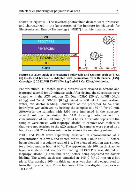
Interface engineering for polymer solar cells 93
shown in Figure 61. The inverted photovoltaic devices were processed and characterized in the laboratories of the Institute for Materials for Electronics and Energy Technology (I-MEET) in ambient atmosphere.
Figure 61: Layer stack of investigated solar cells and SAM molecules: (a) C6, (b) C60-C6 and (c) C60-C18. Adapted with permission from Reference [155]. Copyright © 2012, WILEY-VCH Verlag GmbH & Co. KGaA, Weinheim.
Pre-structured ITO coated glass substrates were cleaned in acetone and isopropyl alcohol for 10 minutes each. After drying, the substrates were coated with the AZO solution (Zn(OAc)2*2H2O (20 g), Al(OH)(OAc)2 (0.3 g) and Zonyl FSO-100 (0.6 g) mixed in 200 ml of demineralized water) via doctor blading. Conversion of the precursor to AZO via hydrolysis was achieved by heating the samples to 150 °C for 10 min. Afterwards the samples with SAM were immersed in the isopropyl alcohol solution containing the SAM forming molecules with a concentration of ca. 0.01 mmol/l for 24 hours. After SAM deposition the samples were rinsed with isopropyl alcohol to remove SAM molecules that were not attached to the AZO surface. The samples were placed on a hot plate at 60 °C for three minutes to remove the remaining solvent. P3HT and PCBM were separately dissolved in chlorobenzene at a concentration of 2 wt% and stirred for at least 1 hour at 60 °C before being blended in a volume ratio of 1:1. The blended solution was stirred for at least another hour at 60 °C. The approximately 100 nm thick active layer was deposited via doctor blading. PEDOT:PSS was diluted in isopropyl alcohol (1:3 volume ratio) before being deposited via doctor blading. The whole stack was annealed at 140 °C for 10 min on a hot plate. Afterwards, a 100 nm thick Ag layer was thermally evaporated to form the top electrode. The active area of the investigated devices was 10.4 mm².

94 Interface engineering for polymer solar cells
6.2.2 Characterization of SAM-modified AZO layers Figure 62 (a) shows an AFM image obtained in tapping mode for an AZO layer fabricated as described above. Figure 62 (b) illustrates the etching and partial disintegration of the particle-like AZO layer at high concentrations of the SAM molecules in the isopropyl alcohol solution (approximately 0.1 mmol/l) due to the acidic nature of the phosphonic acid anchor group. Similar effects have been observed by Hau et al. for the deposition of C60-functionalized alkyl phosphonic acids on ZnO.154 Therefore, a suitable procedure with adapted concentration of the SAM solution and reduced reaction time in the solution was ascertained for a proper deposition of the SAMs.
Figure 62: AFM images of the particle-like AZO layer (a) and etching damage of the AZO layer at higher concentrations (approx. 0.1 mmol/l) of phosphonic acids in the SAM solution (b).
The SAM deposition on the AZO layers was monitored with SCA and c-AFM measurements. Applying a SAM molecule concentration of 0.01 mmol/l and a deposition time of 24 hours, the average water SCA values raised from 50.8° measured for the reference sample without SAM treatment to 120.6° for C6, 77.2° for C60-C6 and 75.7° for C60-C18 and confirmed the formation of densely packed SAMs. In literature, hydrophobic alkyl phosphonic acids were found to show large contact angles (> 95°), while C60 terminated SAMs resulted in layers with smaller contact angles on aluminum oxide.124, 156 The morphology and coverage of the SAMs on reference AZO layers was confirmed by c-AFM measurements (Figure 63). Proper termination of the ZnO surface resulted in a reduction of the current (integral over all pixels) by one order in magnitude for both investigated SAMs.

Interface engineering for polymer solar cells 95
Figure 63: c-AFM measurements on bare AZO, AZO covered with C6-SAM and C60-C6-SAM. “Integrated Current” resembles the addition of the currents for all pixels. Adapted with permission from Reference [155]. Copyright © 2012, WILEY-VCH Verlag GmbH & Co. KGaA, Weinheim.
6.2.3 Electrical characterization of solar cells j-V characteristics were measured with a source measurement unit from BoTest. Illumination was provided by an OrielSol 1A Solarsimulator with AM1.5G spectra at 0.1 W/cm2.
Figure 64: j-V characteristics of best solar cells (a) and corresponding logarithmic plot of dark j-V characteristics (b). Adapted with permission from Reference [155]. Copyright © 2012, WILEY-VCH Verlag GmbH & Co. KGaA, Weinheim.
-0.6 -0.4 -0.2 0 0.2 0.4 0.6 0.8 1.0 1.2-15
-10
-5
0
5
10
15
Curre
nt d
ensi
ty (m
A/cm
²)
Voltage (V)-0.6 0 0.6 1.2 1.8
10-3
10-2
10-1
100
101
102
103
Curre
nt d
ensi
ty ( m
A/cm
²)
Voltage (V)
AZO AZO-SAM(C6) AZO-SAM(C60-C6) AZO-SAM(C60-C18)
(a) (b)

96 Interface engineering for polymer solar cells
The reference cells with only the AZO EEL have an open circuit voltage (VOC) of 602 mV, a short circuit current density (jSC) of -9.23 mA/cm², a fill factor (FF) of 51.9 % and a power conversion efficiency (PCE) of 2.88 %. The series resistance (RS) is 1.2 Ωcm² and the parallel resistance (RP) is 655 Ωcm². Deposition of the C6 SAM deteriorates the device performance. The VOC drops to 354 mV, the jSC to -3.94 mA/cm², and the FF is reduced to 25.3 %. Consequently, the PCE drops down to 0.38 % (see Figure 64 and Table 14 for complete data). The j-V characteristics show an s-shape commonly referred to as second diode behavior. The occurrence of an s-shape was discussed in terms of surface recombination,157 work function mismatch and interface barrier,153, 158 or low transport properties.153 Here, the s-shape is ascribed to the insulating layer formed by the short alkane chains, which is probably best understood as interface barrier with low transport properties. As a result, the non-conductive alkane chains hinder the charge transfer from PCBM to AZO, and the RS of the devices is increased to 9.5 Ωcm². The RP is increased to 1011 Ωcm², which is due to the decoration of the AZO nanoparticles by an insulating nanolayer, resulting in a suppression of the leakage current density. The solar cells with a C60-C6 SAM modified AZO EEL show a drastically improved performance as compared to alkane based SAMs. On the average, the C60-C6 terminated AZO does indeed perform slightly better than the pristine AZO reference.
Table 14: Key parameter set of the solar cells: Average of at least 5 cells on a typical substrate. “Best” corresponds to the best cell on the substrate.
Device VOC (mV)
jSC (mAcm-2)
FF (%)
PCE (%)
RS (Ωcm²)
RP (Ωcm²)
AZO [Best]
602 [620]
-9.23 [-9.00]
51.9 [53.6]
2.88 [2.98]
1.2 [1.2]
655 [692]
AZO-(C6) [Best]
354 [398]
-3.94 [-5.48]
25.3 [28.7]
0.38 [0.63]
9.5 [9.9]
1011 [1141]
AZO-(C60-C6) [Best]
583 [578]
-9.92 [-10.46]
57.4 [57.1]
3.32 [3.46]
0.6 [0.6]
1473 [919]
AZO-(C60-C18) [Best]
584 [577]
-9.24 [-9.90]
53.5 [56.8]
2.88 [3.25]
0.9 [0.6]
1353 [887]

Interface engineering for polymer solar cells 97
The performance data of the C60-C6 terminated AZO yield a VOC of 583 mV, a jSC of -9.92 mA/cm², a FF of 57.4 %, and a PCE of 3.32 %. The improvement is mainly due to an increased FF and a slightly higher jSC. The parallel resistance increases up to 1473 Ωcm², obviously due to the same mechanism as for the C6 SAM. In addition to that, the fullerene at the end of the alkane chain does successfully mediate charge transfer from the active layer into the AZO. The good series resistance together with the increased parallel resistance explains the better FF compared to the reference device. Hau et al. ascribed the jSC increase to an improved morphology of the active layer, induced by the surface energy modification at the interface.151 A better stratification of the fullerene – polymer microstructure is known to suppress recombination at the EEL/active layer interface. Finally, it was verified that the length of the alkane chain in the SAM forming fullerene molecules only slightly influences the charge transport processes. The performance of best devices incorporating C60-C18 SAMs is almost comparable to the cells with a short spacer chain (see Figure 64). In particular the injected current density is equal for both fullerene containing SAMs, which proves that the increased spacer chain length from 6 to 18 units is not hindering the charge transfer between AZO and the organic semiconductor bulk. One explanation for this observation is that the Fullerene SAMs assemble in a densely packed but disordered manner with random distribution of C60 moieties within the layer thickness. A C60-C18 SAM on flat AlOx was found to be only 2.5 nm thick, while the fully stretched molecule is 3.5 nm long.156 The same effect was observed on spherical objects with C60-C18 SAMs on ZnO nanorods.159 Assuming a similar assembly behavior of the SAMs on AZO, the alkane chains are compressed or tilted in a way that the fullerene moiety can have direct contact with the AZO, which is certainly favored by the mismatch between the fullerene and the alkane chain/anchoring group. The AFM and c-AFM measurements in Figure 63 strongly support this hypothesis and suggest that such mismatch may preferentially occur at more irregular or rough layer regions, as expected for instance at the intersection of larger ZnO regimes. For the C60 terminated SAM layers, higher current densities are observed specifically at those regimes where the height profile varies. As this behavior applies for both fullerene SAMs, it could explain the similar performance of the solar cells.
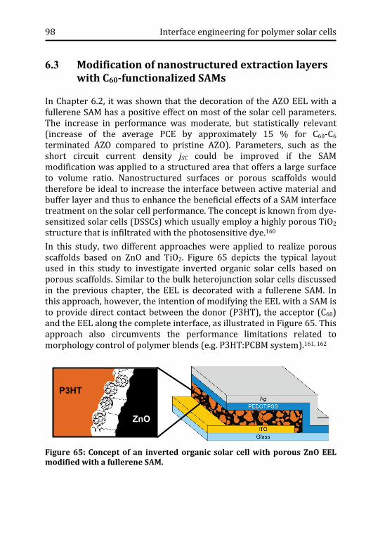
98 Interface engineering for polymer solar cells
6.3 Modification of nanostructured extraction layers with C60-functionalized SAMs
In Chapter 6.2, it was shown that the decoration of the AZO EEL with a fullerene SAM has a positive effect on most of the solar cell parameters. The increase in performance was moderate, but statistically relevant (increase of the average PCE by approximately 15 % for C60-C6 terminated AZO compared to pristine AZO). Parameters, such as the short circuit current density jSC could be improved if the SAM modification was applied to a structured area that offers a large surface to volume ratio. Nanostructured surfaces or porous scaffolds would therefore be ideal to increase the interface between active material and buffer layer and thus to enhance the beneficial effects of a SAM interface treatment on the solar cell performance. The concept is known from dye-sensitized solar cells (DSSCs) which usually employ a highly porous TiO2 structure that is infiltrated with the photosensitive dye.160
In this study, two different approaches were applied to realize porous scaffolds based on ZnO and TiO2. Figure 65 depicts the typical layout used in this study to investigate inverted organic solar cells based on porous scaffolds. Similar to the bulk heterojunction solar cells discussed in the previous chapter, the EEL is decorated with a fullerene SAM. In this approach, however, the intention of modifying the EEL with a SAM is to provide direct contact between the donor (P3HT), the acceptor (C60) and the EEL along the complete interface, as illustrated in Figure 65. This approach also circumvents the performance limitations related to morphology control of polymer blends (e.g. P3HT:PCBM system).161, 162
Figure 65: Concept of an inverted organic solar cell with porous ZnO EEL modified with a fullerene SAM.
P3HT
ZnO

Interface engineering for polymer solar cells 99
6.3.1 Spray coated ZnO nanorods Before processing the porous layer, the 100 nm thick ITO films on the glass substrates (obtained from PGO) were patterned using a photolithographic approach (etch solution: 12 parts HCl, 1 part HNO3 and 12 parts H2O; etch time: 10 minutes). In the first approach, a solution of ZnO nanorods (NRs) was prepared for the fabrication of the porous scaffold. The NRs were prepared according to the synthesis route of Voigt et al. with a concentration of 50 mg/ml zinc acetate dehydrate in methanol resulting in an approximate length of 50 nm and width of 15 nm.163 The dispersions were spin coated on the ITO substrate in order to obtain a dense film of the ZnO NRs that prevents direct contact of subsequently processed layers with the ITO electrode. Then, a second layer of ZnO NRs was spray coated onto the substrates applying a commercially available airbrush system (purchased from Conrad) to obtain a porous structure formed by randomly distributed ZnO nanorods. The resulting film is shown in Figure 66.
Figure 66: Images of the ZnO nanorod layer taken with a light microscope (magnification 100x) (a) and with an AFM (b).
The light microscope image illustrates the inhomogeneity of the film, characterized by the coffee-ring effect and resulting in height differences of several hundreds of nanometers. The AFM image shows an inhomogeneous, densely packed film of ZnO nanorods, rather than a structure with high porosity. Prior to SAM deposition, the samples were treated with an oxygen plasma (0.2 mbar, 3 minutes) to remove hydrocarbon contamination. The deposition of C60-C6 was done either by immersion of the sample into the solution with a concentration of 0.01 mmol/l in isopropanol and

100 Interface engineering for polymer solar cells
a deposition time of 24 hours or by spin coating approximately 100 µl of the SAM solution onto the ZnO layer. In both cases the samples were rinsed afterwards with isopropanol and dried on a hot plate at 60 °C for 5 minutes. Solutions of the active layer (P3HT or P3HT:PCBM with a volume ratio of 1:1) were prepared in chlorobenzene with a concentration of 2 wt%. 250 µl of the solution were dropped onto the sample and remained on the sample for 5 minutes, allowing the infiltration of the solution into the ZnO layer. The remains of the solution were removed by a spin coating step (20 s at 1000 rpm). AFM images proved that this procedure did not lead to a full coverage of the ZnO layer. Therefore, additional 60 µl of the solution were doctor bladed onto the samples. Then, PEDOT:PSS was diluted in isopropyl alcohol (1:5 volume ratio) before being deposited via doctor blading. The stack was annealed at 140 °C for 10 min on a hot plate. Afterwards, a 100 nm thick Ag layer was thermally evaporated to form the top electrode. The active area of the investigated devices was 10.4 mm². Current density-voltage (j-V) characteristics were measured with a source measurement unit from BoTest. Illumination was provided by an OrielSol 1A Solarsimulator with AM1.5G spectra at 0.1 W/cm2.
Figure 67: j-V characteristics of best solar cells (a) and corresponding logarithmic plot of dark j-V characteristics (b).
The reference cells with only P3HT deposited on the ZnO layer have an average open circuit voltage (VOC) of 496 mV, a short circuit current density (jSC) of -0.39 mA/cm², a fill factor (FF) of 43.2 % and a power conversion efficiency (PCE) of 0.08 %. The series resistance (RS) is 12.0 Ωcm² and the parallel resistance (RP) is 53148 Ωcm².
-0.6 0 0.6 1.2 1.810-5
10-4
10-3
10-2
10-1
100
101
102
Curre
nt d
ensi
ty (m
A/cm
2 )
Voltage (V)
P3HT C60-C6 + P3HT C60-C6(s. c.) + P3HT C60-C6(s. c.) + P3HT:PCBM
-0.6 -0.4 -0.2 0 0.2 0.4 0.6 0.8-4
-2
0
2
4
Curre
nt d
ensi
ty (m
A/cm
2 )
Voltage (V)
(a) (b)

Interface engineering for polymer solar cells 101
Table 15: Key parameter set of the solar cells: Average of at least 3 cells on a typical substrate. “Best” corresponds to the best cell on the substrate. Device VOC
(mV) jSC (mAcm-2)
FF (%)
PCE (%)
RS (Ωcm²)
RP (Ωcm²)
P3HT [Best]
496 [519]
-0.39 [-0.46]
43.2 [42.5]
0.08 [0.10]
12.0 [9.3]
53148 [44025]
C60-C6 + P3HT [Best]
293 [320]
-0.84 [-0.79]
42.8 [43.9]
0.11 [0.11]
12.6 [10.8]
5031 [3147]
C60-C6 (s. c.) + P3HT [Best]
314 [340]
0.86 [-0.88]
43.4 [46.6]
0.12 [0.14]
19.2 [19.6]
6192 [4486]
C60-C6 (s. c.) + P3HT:PCBM [Best]
387 [382]
1.59 [-1.90]
43.5 [41.2]
0.27 [0.30]
35.9 [31.4]
14156 [3973]
Deposition of the C60-C6 SAM improves the device performance slightly. The jSC rises to -0.84 mA/cm² (immersed) and -0.86 mA/cm² (spin coated). Using the P3HT:PCBM blend as the active material leads to an additional improvement (VOC = 387 mV, jSC = -1.59 mA/cm², FF = 43.5 % and PCE = 0.27 %) compared to the samples with neat P3HT (see Figure 67 and Table 15 for complete data). The VOC of the devices without SAM modification of the ZnO are lower than values found in the literature for similar heterojunction solar cells. Hau et al. investigated inverted heterojunction solar cells with P3HT as the active material and a thin layer of ZnO nanoparticles as EEL and obtained a much higher VOC of 0.66 V, a jSC of 1.28 mA/cm2, a FF of 37.8 % and PCE of 0.32 %.154 They found that by modifying the ZnO layer with a fullerene SAM the jSC, FF and PCE are increased significantly, while the VOC decreases. This was attributed to the interfacial dipole formed by the anchor group of the SAM. They explained that in bulk heterojunction solar cells with P3HT:PCBM blends as the active material the detrimental impact of the SAM modification on the VOC was not observable due to the larger interface between P3HT (donor) and PCBM (acceptor) compared to the heterojunction with P3HT as the donor and the C60 SAM as the acceptor. The low short-circuit currents obtained in the devices could indicate high recombination losses at the interfaces. Modification of the ZnO surface with the C60 SAM reduces the recombination and thus the jSC increases considerably, as was also observed in Chapter 6.2 for the bulk heterojunction devices and in other studies.151, 154

102 Interface engineering for polymer solar cells
6.3.2 Highly ordered TiO2 nanotube arrays Another approach presented in various studies is the application of ordered heterojunctions. This concept is also based on the infiltration of highly ordered porous structures and has been demonstrated for well-alligned ZnO nanorods and TiO2 nanotubes (NTs).164-170 Oriented TiO2-NT arrays prepared by anodization of titanium metal combine high surface area with well-defined pore geometry and have been investigated in dye sensitized solar cells as an attractive alternative to films fabricated by the sol-gel route. While the fabrication of such nanostructures has been extensively investigated and optimized for anodization of titanium foils,171, 172 there exist only few reports on the realization of the TiO2 NT growth from titanium thin films on glass substrates that could be used for the fabrication of semi-transparent solar cells.168-170 In this second approach TiO2 NT arrays were grown from evaporated thin films of titanium on ITO covered glass slides. The nanotube arrays were employed as transport layer for electrons and have been decorated with fullerene SAM. The standard procedure for SAM deposition described in Chapter 3 has also been applied for this type of samples. It has been shown that phosphonic acids form strong and stable bonds after adsorption on TiO2.173, 174 The TiO2-NT fabrication on the ITO covered glass substrates was conducted at the Chair for Surface Science and Corrosion (FAU Erlangen-Nürnberg), the final solar cell fabrication was carried out at I-MEET. After patterning the ITO, the substrates were ultrasonicated in deionized water, actone and isopropyl alcohol. Then the samples were covered with an approximately 300 nm thick titanium layer. The evaporation of titanium (purity of Ti ≈ 99.99 %) was carried out at a pressure in the range of 10-6 mbar and an evaporation rate of 0.1 nm/s. The nanotubes were formed by anodic oxidation, using electrolyte based on ethylene glycol with 0.1 M NH4F and a maximum potential of 45 V, resulting in a nanotube layer thickness of approximately 600 nm. It was not possible to obtain completely uniform NT arrays, since the applied anodization potential was not homogeneously distributed over the whole device area (the current was higher in the center than in the margins of the sample). Other issues related to non-uniform TiO2-NTs formed from evaporated titanium layers is the bad adhesion of Ti on ITO that can lead to delamination. Thus, the pre-treatment of the surfaces before the titanium evaporation and the evaporation conditions are crucial for the
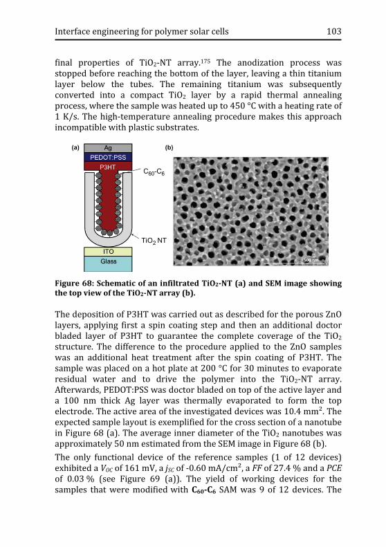
Interface engineering for polymer solar cells 103
final properties of TiO2-NT array.175 The anodization process was stopped before reaching the bottom of the layer, leaving a thin titanium layer below the tubes. The remaining titanium was subsequently converted into a compact TiO2 layer by a rapid thermal annealing process, where the sample was heated up to 450 °C with a heating rate of 1 K/s. The high-temperature annealing procedure makes this approach incompatible with plastic substrates.
Figure 68: Schematic of an infiltrated TiO2-NT (a) and SEM image showing the top view of the TiO2-NT array (b).
The deposition of P3HT was carried out as described for the porous ZnO layers, applying first a spin coating step and then an additional doctor bladed layer of P3HT to guarantee the complete coverage of the TiO2 structure. The difference to the procedure applied to the ZnO samples was an additional heat treatment after the spin coating of P3HT. The sample was placed on a hot plate at 200 °C for 30 minutes to evaporate residual water and to drive the polymer into the TiO2-NT array. Afterwards, PEDOT:PSS was doctor bladed on top of the active layer and a 100 nm thick Ag layer was thermally evaporated to form the top electrode. The active area of the investigated devices was 10.4 mm². The expected sample layout is exemplified for the cross section of a nanotube in Figure 68 (a). The average inner diameter of the TiO2 nanotubes was approximately 50 nm estimated from the SEM image in Figure 68 (b). The only functional device of the reference samples (1 of 12 devices) exhibited a VOC of 161 mV, a jSC of -0.60 mA/cm², a FF of 27.4 % and a PCE of 0.03 % (see Figure 69 (a)). The yield of working devices for the samples that were modified with C60-C6 SAM was 9 of 12 devices. The

104 Interface engineering for polymer solar cells
solar cells exhibited an average VOC of 285 mV, a jSC of -2.11 mA/cm², a FF of 31.4 % and a PCE of 0.21 %. The j-V characteristic of the best device (PCE = 0.55 %) is depicted in Figure 69 (a). It could not be proven if the P3HT was successfully infiltrated into the nanotubes (see SEM image in Figure 69), which could be one reason for the rather bad performance compared to similar devices published by Mor et al. They used TiO2-NTs with a length of 270 nm and a pore size of 50 nm and successfully infiltrated the pores with a P3HT:PCBM blend and obtained a VOC of 641 mV, a jSC of -12.43 mA/cm², a FF of 51.1 % and a PCE of 4.07 %.168 In another study, they obtained an increase of the PCE from 0.34 % for TiO2 NTs infiltrated with neat P3HT to 3.2 % by modifying the TiO2-NTs with an organic dye.169
Figure 69: j-V characteristics of best solar cells for reference sample and for SAM modified sample (a); SEM image of nanotubes after the solar cell fabrication (b).
6.4 Summary
In conclusion, the possibility of fine-tuning buffer layers in polymer solar cells by interface modification with SAMs has been demonstrated. The successful and rather complete decoration of the AZO surface with phosphonic acid anchored SAMs was proven and resulted in a modification of the electronic properties of the AZO. SAM modification of AZO electrodes resulted in an increased parallel resistance. SAM layers without a covalently linked fullerene form an insulating barrier, which increases series resistance and deteriorates the device performance significantly. By employing the fullerene SAM, the charge transfer from PCBM to AZO is improved, and the series resistance is reduced while the
(a) (b)
-0.6 -0.4 -0.2 0 0.2 0.4 0.6 0.8-4
-2
0
2
4TiO2 nanotubes
w/o SAM with SAM
Curre
nt d
ensi
ty (m
A/cm
2 )
Voltage (V)
PCE = 0.55 %

Interface engineering for polymer solar cells 105
shunt resistance remains high. As a result, the average solar cell efficiency could be improved by approximately 15 % from 2.9 to 3.3 %. For the approaches based on the application of porous charge extraction layers, it was observed that the modification with the fullerene SAM had a beneficial effect on the device performance. However, the solar cell performance for this approach was generally low compared to the bulk heterojunction concept. The study shows that the introduction of such porous structures into the solar cell architecture of a (bulk) heterojunction solar cell is very challenging. The greatest challenge in this approach seems to be the wetting behavior and the infiltration of such structures with the active materials. A more detailed investigation of the crucial properties impacting the infiltration behavior will be necessary for further improvements. Among others, this includes analysis of the surface energy of the structures and the viscosity of the solutions and the processing conditions applied for the infiltration of the active material.


Summary 107
7. Summary
This work presents a study on the effect of densely packed dipolar self-assembled monolayers (SAMs) on the threshold voltage (VTH) of organic thin-film transistors OTFTs. The SAMs were employed as part of a hybrid dielectric on ultra-thin plasma-oxidized aluminum oxide and on thicker aluminum oxide layers with varying thickness processed by atomic layer deposition. A detailed characterization was carried out in order to determine the electrostatic potentials of the SAMs. X-ray reflectivity (XRR) experiments were applied to determine the SAM thickness, X-ray photoelectron spectroscopy (XPS) measurements to estimate the SAM packing density, capacitance measurements to determine the relative permittivity and density functional theory (DFT) calculations to compute the respective dipole moments. The results of this study provide evidence for the quantitative relationship between the electrostatic potential of a SAM and the threshold voltage shift observed in OTFT transfer characteristics. The generality of the relationship was demonstrated for both p-type (pentacene, DH6T) and n-type (C60) semiconductors. It was also shown that the absolute threshold voltage depends on the work function of the semiconductor. Consequently, this study offers a consistent explanation for the large threshold voltage shifts of several tens of volts reported for thick SAM-modified SiO2 dielectrics in literature. The proposed model in Chapter 4.4.3 provides a general approach for predicting VTH-values for OTFTs with SAM-modified dielectrics. Thus, SAMs can be regarded as a valuable tool for the design of integrated circuits (ICs), where it is important to ensure the circuit´s immunity against electrical noise by exact adjustment of the switching voltage. A second important benefit is the possibility to reduce the supply voltage of an IC by reducing the absolute value of the threshold voltage with a suitable SAM treatment. The accurateness of each analytical method applied for the SAM characterization limited the correctness of the theoretical predictions. Nevertheless, the fair agreement between theoretical calculations and experimentally determined threshold voltage values led to the conclusions presented in this work. The results of this study are valuable tools for future research on OTFT devices that exhibit densely packed dipolar layers at the interface of dielectric and semiconductor.

108 Summary
In general, mixed SAMs of molecules with different dipole moments provide the possibility to continuously tune VTH. SAM molecules exhibiting a large dipole moment and redox-activity have an impact on the shift of the transfer characteristic and on the hysteresis. By introducing redox-active C60 functionalized molecules into pure and mixed SAMs, it was shown that the two effects can be clearly distinguished and that the hysteresis of the transfer characteristic can be explicitly attributed to the redox properties of the SAM molecules. Consequently, the magnitude of the hysteresis can be correlated with the amount of redox-active molecules in the SAM. The C60 functionalized molecules also served as photoactive moieties in pure and mixed SAMs. The concept presented in Chapter 5 demonstrated the versatility of these SAM molecules that led to an enhanced photoresponsivity compared to devices without photoactive SAMs. It was further shown that the interface properties dictated by the photoactive SAM have an impact on the dynamics of the photo induced charge transfer in such OTFT devices. Finally, it was demonstrated that SAM treatments of charge transport layers in organic solar cells can have a beneficial effect on the performance. The PCE of inverted P3HT:PCBM bulk-heterojunction solar cells was increased by approximately 15 % from 2.9 to 3.3 % by modifying the Al-doped ZnO electron extraction layer (EEL) with a C60 functionalized SAM. The beneficial effect of a SAM treatment was also demonstrated for nanostructured EELs, such as spray coated ZnO nanorod and TiO2 nanotube layers.
Zusammenfassung 109
8. Zusammenfassung
In dieser Arbeit wurde der Einfluss von selbst organisierten Monolagen (SAMs) auf die Schwellspannung von organischen Dünnschichttran-sistoren (OTFTs) untersucht. Die SAMs wurden dabei als Bestandteil von hybriden Dielektrika sowohl auf dünnen, plasmaoxidierten Aluminium-oxidschichten als auch auf dickeren Aluminiumoxidschichten, die über Atomlagenabscheidung hergestellt wurden, eingesetzt. Eine detaillierte Charakterisierung der SAMs ermöglichte die Berechnung des elektro-statischen Potentials der SAMs. Röntgenreflektometrie (XRR), Röntgen-photoelektronenspektroskopie (XPS) und Kapazitätsmessungen wurden eingesetzt, um die Dicke, die Packungsdichte und die relative Permittivität der SAMs zu ermitteln. Die computerbasierte Berechnung der Dipolmomente der SAMs erfolgte mithilfe der Methode der Dichte-funktionaltheorie (DFT). Die Ergebnisse in dieser Arbeit belegen, dass zwischen dem elektro-statischen Potential der SAM und der Verschiebung der Transistor-Schwellspannung ein quantitativer Zusammenhang besteht. Die Allge-meingültigkeit dieses Zusammenhangs wurde sowohl für p-Halbleiter (Pentacen, DH6T) als auch für n-Halbleiter (C60) gezeigt. Es wurde weiterhin gezeigt, dass die Schwellspannung von der Austrittsarbeit des Halbleiters abhängt. Das in dieser Arbeit beschriebene Modell beschreibt den Effekt des SAM Dipolmoments auf die Ladungsträgerdichte im angrenzenden Halbleiter und bietet die Möglichkeit, Schwellspannungen von OTFTs mit SAM-modifizierten Dielektrika zu berechnen. Die gezielte Einstellung von Transistor-Schwellspannungen mithilfe von SAMs bietet vor allem in Bezug auf die Störanfälligkeit von Integrierten Schaltungen (ICs) entscheidende Vorteile. Die Genauigkeit der Berechnung von elektrostatischen Potentialen wurde durch die Genauigkeit der angewendeten analytischen Methoden begrenzt. Trotz dieser Einschränkung zeigten die experimentell be-stimmten Transistor-Kennwerte und die theoretischen Berechnungen eine gute Übereinstimmung. Somit stellen die Ergebnisse dieser Arbeit ein wertvolles Hilfsmittel für die weitere Forschung an OTFTs mit SAM-modifizierten Dielektrika dar.

110 Zusammenfassung
SAM-Moleküle mit Elektronenakzeptor-Eigenschaften (z. B. C60) haben einen wesentlichen Einfluss auf die Hysterese in der OTFT Transfer-Charakteristik. Dies wurde durch gemischte SAMs, die C60-funktiona-lisierte SAM-Moleküle in unterschiedlichen Konzentrationen beinhal-teten, gezeigt. Die beobachtete Schwellspannungs-Verschiebung sowie auch die Hysterese konnten hierbei eindeutig der jeweils dafür verantwortlichen Eigenschaft (Dipolmoment und Elektronenakzeptor-Eigenschaft) zugeordnet werden. C60-funktionalisierte SAM-Moleküle wurden ebenso für die Herstellung von photosensitiven OTFTs verwendet. Durch den Einsatz der C60-funktionalisierten SAM-Moleküle im hybriden Dielektrikum konnte die Lichtempfindlichkeit der Bauteile gegenüber OTFTs ohne C60-funktiona-lisierte SAM-Moleküle deutlich gesteigert werden. Des Weiteren konnte beobachtet werden, dass die C60-funktionalisierten SAM-Moleküle einen wesentlichen Einfluss auf die Zeitabhängigkeit des photoinduzierten Ladungstransfers an der Grenzfläche von SAM und Halbleiter haben. Im letzten Abschnitt dieser Arbeit wurde gezeigt, dass eine geeignete SAM-Modifizierung von Ladungsträgertransportschichten einen positiv-en Effekt auf den Wirkungsgrad von organischen Solarzellen haben kann. Durch die Modifizierung einer Al-dotierten ZnO Elektronentransport-schicht mit einer C60-funktionalisierten SAM konnte der Wirkungsgrad von P3HT:PCBM Solarzellen um 15 % von 2.9 % auf 3.3 % gesteigert werden. Der positive Effekt einer SAM-Modifizierung auf den Wirkungs-grad wurde auch für organische Solarzellen mit nanostrukturierten Ladungsträgertransportschichten bestehend aus aufgesprühten ZnO-Nanorods oder geordneten TiO2-Nanotube Schichten erzielt.

Bibliography 111
9. Bibliography
1. Press release. http://www.osram.de/osram_de/ (October, 2013). 2. Koch, N. Organic electronic devices and their functional interfaces.
ChemPhysChem 8, 1438-1455 (2007). 3. Press release. http://www.plasticlogic.com/ (October, 2013). 4. Press release. http://www.polyic.de/ (October, 2013). 5. Press release. http://www.heliatek.com/ (October, 2013). 6. Yip, H.-L., Hau, S.K., Baek, N.S., Ma, H. & Jen, A.K.Y. Polymer Solar Cells
That Use Self-Assembled-Monolayer-Modified ZnO/Metals as Cathodes. Advanced Materials 20, 2376-2382 (2008).
7. Ma, H., Yip, H.-L., Huang, F. & Jen, A.K.Y. Interface Engineering for Organic Electronics. Advanced Functional Materials 20, 1371-1388 (2010).
8. Ma, H., Acton, O., Hutchins, D.O., Cernetic, N. & Jen, A.K.Y. Multifunctional phosphonic acid self-assembled monolayers on metal oxides as dielectrics, interface modification layers and semiconductors for low-voltage high-performance organic field-effect transistors. Physical Chemistry Chemical Physics 14, 14110-14126 (2012).
9. Gundlach, D.J., Jia, L. & Jackson, T.N. Pentacene TFT with improved linear region characteristics using chemically modified source and drain electrodes. IEEE Electron Device Letters 22, 571-573 (2001).
10. Klauk, H. et al. High-mobility polymer gate dielectric pentacene thin film transistors. Journal of Applied Physics 92, 5259-5263 (2002).
11. Yang, H. et al. Conducting AFM and 2D GIXD studies on pentacene thin films. Journal of the American Chemical Society 127, 11542-11543 (2005).
12. Asadi, K., Wu, Y., Gholamrezaie, F., Rudolf, P. & Blom, P.W.M. Single-layer pentacene field-effect transistors using electrodes modified with self-assembled monolayers. Advanced Materials 21, 4109-4114 (2009).
13. Yang, S.Y., Kim, S.H., Shin, K., Jeon, H. & Park, C.E. Low-voltage pentacene field-effect transistors with ultrathin polymer gate dielectrics. Applied Physics Letters 88, 173507 (2006).
14. Kim, S.H. et al. Low-operating-voltage pentacene field-effect transistor with a high-dielectric-constant polymeric gate dielectric. Applied Physics Letters 89, 183516 (2006).
15. Halik, M. et al. Low-voltage organic transistors with an amorphous molecular gate dielectric. Nature 431, 963-966 (2004).
112 Bibliography
16. Klauk, H., Zschieschang, U., Pflaum, J. & Halik, M. Ultralow-power organic complementary circuits. Nature 445, 745-748 (2007).
17. Halik, M. & Hirsch, A. The potential of molecular self-assembled monolayers in organic electronic devices. Advanced Materials 23, 2689-2695 (2011).
18. Whitesides, G.M. & Boncheva, M. Beyond molecules: Self-assembly of mesoscopic and macroscopic components. Proceedings of the National Academy of Sciences of the United States of America 99, 4769-4774 (2002).
19. Ulman, A. Formation and Structure of Self-Assembled Monolayers. Chemical Reviews 96, 1533-1554 (1996).
20. Schreiber, F. et al. Adsorption mechanisms, structures, and growth regimes of an archetypal self-assembling system: Decanethiol on Au(111). Physical Review B 57, 12476-12481 (1998).
21. Schreiber, F. Structure and growth of self-assembling monolayers. Progress in Surface Science 65, 151-257 (2000).
22. Bain, C.D. & Whitesides, G.M. Correlations between wettability and structure in monolayers of alkanethiols adsorbed on gold. Journal of the American Chemical Society 110, 3665-3666 (1988).
23. Bain, C.D. et al. Formation of monolayer films by the spontaneous assembly of organic thiols from solution onto gold. Journal of the American Chemical Society 111, 321-335 (1989).
24. Bain, C.D., Evall, J. & Whitesides, G.M. Formation of monolayers by the coadsorption of thiols on gold: variation in the head group, tail group, and solvent. Journal of the American Chemical Society 111, 7155-7164 (1989).
25. Love, J.C., Estroff, L.A., Kriebel, J.K., Nuzzo, R.G. & Whitesides, G.M. Self-Assembled Monolayers of Thiolates on Metals as a Form of Nanotechnology. Chemical Reviews 105, 1103-1170 (2005).
26. Dulcey, C.S. et al. Deep UV Photochemistry of Chemisorbed Monolayers: Patterned Coplanar Molecular Assemblies. Science 252, 551-554 (1991).
27. Tiberio, R.C. et al. Self-assembled monolayer electron beam resist on GaAs. Applied Physics Letters 62, 476 (1993).
28. Lercel, M.J. et al. Pattern transfer of electron beam modified self-assembled monolayers for high-resolution lithography. Journal of Vacuum Science & Technology B 13, 1139-1143 (1995).
29. Whelan, C.S., Lercel, M.J., Craighead, H.G., Seshadri, K. & Allara, D.L. Improved electron-beam patterning of Si with self-assembled monolayers. Applied Physics Letters 69, 4245 (1996).

Bibliography 113
30. Whidden, T.K. et al. Pattern transfer to silicon by microcontact printing and RIE. Nanotechnology 7, 447-451 (1996).
31. Wilbur, J.L., Kumar, A., Kim, E. & Whitesides, G.M. Microfabrication by microcontact printing of self-assembled monolayers. Advanced Materials 6, 600-604 (1994).
32. Vuillaume, D., Boulas, C., Collet, J., Davidovits, J.V. & Rondelez, F. Organic insulating films of nanometer thicknesses. Applied Physics Letters 69, 1646-1648 (1996).
33. Bashir, A. et al. High-Performance Zinc Oxide Transistors and Circuits Fabricated by Spray Pyrolysis in Ambient Atmosphere. Advanced Materials 21, 2226-2231 (2009).
34. Gao, W., Dickinson, L., Grozinger, C., Morin, F.G. & Reven, L. Self-Assembled Monolayers of Alkylphosphonic Acids on Metal Oxides. Langmuir 12, 6429-6435 (1996).
35. Schwartz, D.K. Mechanisms and kinetics of self-assembled monolayer formation. Annual Review of Physical Chemistry 52, 107-137 (2001).
36. Hotchkiss, P.J. et al. The modification of indium tin oxide with phosphonic acids: Mechanism of binding, tuning of surface properties, and potential for use in organic electronic applications. Accounts of Chemical Research 45, 337-346 (2012).
37. Luschtinetz, R. et al. Adsorption of phosphonic and ethylphosphonic acid on aluminum oxide surfaces. Surface Science 602, 1347-1359 (2008).
38. Ramsier, R.D., Henriksen, P.N. & Gent, A.N. Adsorption of phosphorus acids on alumina. Surface Science 203, 72-88 (1988).
39. Luschtinetz, R., Oliveira, Augusto F., Duarte, Hélio A. & Seifert, G. Self-assembled Monolayers of Alkylphosphonic Acids on Aluminum Oxide Surfaces - A Theoretical Study. Zeitschrift für anorganische und allgemeine Chemie 636, 1506-1512 (2010).
40. D'Andrea, S.C. & Fadeev, A.Y. Covalent Surface Modification of Calcium Hydroxyapatite Using n-Alkyl- and n-Fluoroalkylphosphonic Acids. Langmuir 19, 7904-7910 (2003).
41. Bumm, L.A., Arnold, J.J., Dunbar, T.D., Allara, D.L. & Weiss, P.S. Electron Transfer through Organic Molecules. Journal of Physical Chemistry B 103, 8122-8127 (1999).
42. Geisse, N.A. AFM and combined optical techniques. Materials Today 12, 40-45 (2009).
43. Ellison, D.J., Lee, B., Podzorov, V. & Frisbie, C.D. Surface potential mapping of SAM-functionalized organic semiconductors by Kelvin probe force microscopy. Advanced Materials 23, 502-507 (2011).

114 Bibliography
44. Kuna, J.J. et al. The effect of nanometre-scale structure on interfacial energy. Nature Materials 8, 837-842 (2009).
45. Aswal, D.K., Lenfant, S., Guerin, D., Yakhmi, J.V. & Vuillaume, D. Self assembled monolayers on silicon for molecular electronics. Analytica Chimica Acta 568, 84-108 (2006).
46. Lagutchev, A.S., Song, K.J., Huang, J.Y., Yang, P.K. & Chuang, T.J. Self-assembly of alkylsiloxane monolayers on fused silica studied by XPS and sum frequency generation spectroscopy. Chemical Physics 226, 337-349 (1998).
47. Hauffman, T. et al. Study of the Self-Assembling of n-Octylphosphonic Acid Layers on Aluminum Oxide. Langmuir 24, 13450-13456 (2008).
48. Moulder, J.F., Stickle, W.F., Sobol, P.E. & Bomben, K.D. Handbook of X Ray Photoelectron Spectroscopy (Perkin-Elmer Corporation, 1992).
49. DeLongchamp, D.M., Kline, R.J., Fischer, D.A., Richter, L.J. & Toney, M.F. Molecular characterization of organic electronic films. Advanced Materials 23, 319-337 (2011).
50. Wasserman, S.R. et al. The structure of self-assembled monolayers of alkylsiloxanes on silicon: a comparison of results from ellipsometry and low-angle x-ray reflectivity. Journal of the American Chemical Society 111, 5852-5861 (1989).
51. Argekar, S.U., Kirley, T.L. & Schaefer, D.W. Determination of structure-property relationships for 3-aminopropyltriethoxysilane films using x-ray reflectivity. Journal of Materials Research 28, 1118-1128 (2013).
52. Dong, X., Wang, P., Argekar, S. & Schaefer, D.W. Structure and composition of trivalent chromium process (TCP) films on Al alloy. Langmuir 26, 10833-10841 (2010).
53. Kim, H.J. et al. Adsorption kinetics of alkanethiols studied by quartz crystal microbalance. Thin Solid Films 327–329, 191-194 (1998).
54. Gannon, G., Greer, J.C., Larsson, J.A. & Thompson, D. Molecular Dynamics Study of Naturally Occurring Defects in Self-Assembled Monolayer Formation. ACS Nano 4, 921-932 (2010).
55. Vuillaume, D. Molecular-scale electronics. Comptes Rendus Physique 9, 78-94 (2008).
56. DiBenedetto, S.A., Facchetti, A., Ratner, M.A. & Marks, T.J. Charge Conduction and Breakdown Mechanisms in Self-Assembled Nanodielectrics. Journal of the American Chemical Society 131, 7158-7168 (2009).
Bibliography 115
57. Maisch, S., Buckel, F. & Effenberger, F. Preparation of High Quality Electrical Insulator Self-Assembled Monolayers on Gold. Experimental Investigation of the Conduction Mechanism through Organic Thin Films. Journal of the American Chemical Society 127, 17315-17322 (2005).
58. Akkerman, H.B., Blom, P.W., de Leeuw, D.M. & de Boer, B. Towards molecular electronics with large-area molecular junctions. Nature 441, 69-72 (2006).
59. Fan, F.-R.F. et al. Charge Transport through Self-Assembled Monolayers of Compounds of Interest in Molecular Electronics. Journal of the American Chemical Society 124, 5550-5560 (2002).
60. Selzer, Y., Salomon, A. & Cahen, D. The Importance of Chemical Bonding to the Contact for Tunneling through Alkyl Chains. Journal of Physical Chemistry B 106, 10432-10439 (2002).
61. Cheng, X. et al. Controlling Electron and Hole Charge Injection in Ambipolar Organic Field-Effect Transistors by Self-Assembled Monolayers. Advanced Functional Materials 19, 2407-2415 (2009).
62. Marmont, P. et al. Improving charge injection in organic thin-film transistors with thiol-based self-assembled monolayers. Organic Electronics 9, 419-424 (2008).
63. Weber, R. et al. Photoemission from Azobenzene Alkanethiol Self-Assembled Monolayers. Journal of Physical Chemistry B 107, 7768-7775 (2003).
64. Smith, M.B. March´s Advanced Organic Chemistry : Reactions, Mechanisms, and Structure (John Wiley & Sons, Inc., 2013).
65. Bruening, M. et al. Simultaneous control of surface potential and wetting of solids with chemisorbed multifunctional ligands. Journal of the American Chemical Society 119, 5720-5728 (1997).
66. Ashkenasy, G., Cahen, D., Cohen, R., Shanzer, A. & Vilan, A. Molecular Engineering of Semiconductor Surfaces and Devices. Accounts of Chemical Research 35, 121-128 (2002).
67. Natan, A., Kronik, L., Haick, H. & Tung, R.T. Electrostatic Properties of Ideal and Non-ideal Polar Organic Monolayers: Implications for Electronic Devices. Advanced Materials 19, 4103-4117 (2007).
68. Cahen, D., Naaman, R. & Vager, Z. The cooperative molecular field effect. Advanced Functional Materials 15, 1571-1578 (2005).
69. Anderson, R.J., Bendell, D.J. & Groundwater, P.W. Organic Spectroscopic Analysis (The Royal Society of Chemistry, 2004).
70. Sze, S.M. Physics of Semiconductor Devices (John Wiley & Sons, Inc., 2007).

116 Bibliography
71. Brütting, W., Adachi, C. & Holmes, R.J. Physics of Organic Semiconductors (Wiley-VCH Verlag GmbH & Co. KGaA, 2012).
72. Horowitz, G., Hajlaoui, R., Bouchriha, H., Bourguiga, R. & Hajlaoui, M. The concept of "threshold voltage" in organic field-effect transistors. Advanced Materials 10, 923-927 (1998).
73. Klauk, H. Organic thin-film transistors. Chemical Society Reviews 39, 2643-2666 (2010).
74. Horowitz, G. in Organic Field-Effect Transistors 73-101 (CRC Press, 2007).
75. Gelinck, G.H. et al. Flexible active-matrix displays and shift registers based on solution-processed organic transistors. Nature Materials 3, 106-110 (2004).
76. Kawaguchi, H., Someya, T., Sekitani, T. & Sakurai, T. Cut-and-paste customization of organic FET integrated circuit and its application to electronic artificial skin. IEEE Journal of Solid-State Circuits 40, 177-185 (2005).
77. Ante, F. et al. Contact resistance and megahertz operation of aggressively scaled organic transistors. Small 8, 73-79 (2012).
78. Horowitz, G. Organic Field-Effect Transistors. Advanced Materials 10, 365-377 (1998).
79. Wong, H.-S., White, M.H., Krutsick, T.J. & Booth, R.V. Modeling of transconductance degradation and extraction of threshold voltage in thin oxide MOSFET's. Solid-State Electronics 30, 953-968 (1987).
80. Zaumseil, J. & Sirringhaus, H. Electron and Ambipolar Transport in Organic Field-Effect Transistors. Chemical Reviews 107, 1296-1323 (2007).
81. Chung, Y. et al. Controlling electric dipoles in nanodielectrics and its applications for enabling air-stable n-channel organic transistors. Nano Letters 11, 1161-1165 (2011).
82. Kobayashi, S. et al. Control of carrier density by self-assembled monolayers in organic field-effect transistors. Nature Materials 3, 317-322 (2004).
83. Pernstich, K.P. et al. Threshold voltage shift in organic field effect transistors by dipole monolayers on the gate insulator. Journal of Applied Physics 96, 6431 (2004).
84. Possanner, S.K., Zojer, K., Pacher, P., Zojer, E. & Schürrer, F. Threshold Voltage Shifts in Organic Thin-Film Transistors Due to Self-Assembled Monolayers at the Dielectric Surface. Advanced Functional Materials 19, 958-967 (2009).
Bibliography 117
85. Fleischli, F.D., Suarez, S., Schaer, M. & Zuppiroli, L. Organic thin-film transistors: The passivation of the dielectric-pentacene interface by dipolar self-assembled monolayers. Langmuir 26, 15044-15049 (2010).
86. Gholamrezaie, F. et al. Charge Trapping by Self-Assembled Monolayers as the Origin of the Threshold Voltage Shift in Organic Field-Effect Transistors. Small 8, 241–245 (2012).
87. Schanz, M., Brockherde, W., Hauschild, R., Hosticka, B.J. & Schwarz, M. Smart CMOS image sensor arrays. IEEE Transactions on Electron Devices 44, 1699-1705 (1997).
88. Narayan, K.S. & Kumar, N. Light responsive polymer field-effect transistor. Applied Physics Letters 79, 1891 (2001).
89. Guo, Y., Yu, G. & Liu, Y. Functional organic field-effect transistors. Advanced Materials 22, 4427-4447 (2010).
90. Cho, M.Y. et al. Gate-field dependent photosensitivity of soluble 1,2,4,5-tetra(5ʹ-hexyl-[2,2ʹ]terthiophenyl-5-vinyl)-benzene based organic thin film transistors. Journal of Applied Physics 108, 023703 (2010).
91. Opitz, A. et al. Bipolar charge transport in organic field-effect transistors: Enabling high mobilities and transport of photo-generated charge carriers by a molecular passivation layer. Organic Electronics 13, 1614-1622 (2012).
92. Debucquoy, M. et al. Correlation between bias stress instability and phototransistor operation of pentacene thin-film transistors. Applied Physics Letters 91, 103508 (2007).
93. Debucquoy, M. Charge Trappin in Organic Field-Effect Transistors and Applications for Photodetectors and Memory Devices. Dissertation, Katholieke Universiteit Leuven (2009).
94. Marjanović, N. et al. Photoresponse of organic field-effect transistors based on conjugated polymer/fullerene blends. Organic Electronics 7, 188-194 (2006).
95. Noh, Y.-Y. et al. High-photosensitivity p-channel organic phototransistors based on a biphenyl end-capped fused bithiophene oligomer. Applied Physics Letters 86, 043501 (2005).
96. Brabec, C.J., Dyakonov, V., Parisi, J. & Sariciftci, N.S. Organic photovoltaics: concepts and realization (Springer, 2003).
97. Seemann, A. Design of Transparent Electrodes and Their Influence on Organic Solar Cells. Dissertation, Friedrich-Alexander-Universität Erlangen-Nürnberg (2010).
98. Puurunen, R.L. Surface chemistry of atomic layer deposition: A case study for the trimethylaluminum/water process. Journal of Applied Physics 97, 121301 (2005).

118 Bibliography
99. Groner, M.D., Fabreguette, F.H., Elam, J.W. & George, S.M. Low-Temperature Al2O3 Atomic Layer Deposition. Chemistry of Materials 16, 639-645 (2004).
100. Kwok, D.Y. & Neumann, A.W. Contact angle measurement and contact angle interpretation. Advances in Colloid and Interface Science 81, 167-249 (1999).
101. Owens, D.K. & Wendt, R.C. Estimation of the surface free energy of polymers. Journal of Applied Polymer Science 13, 1741-1747 (1969).
102. Cohen, A.J., Mori-Sanchez, P. & Yang, W. Insights into current limitations of density functional theory. Science 321, 792-794 (2008).
103. Leboeuf, M., Koster, A.M., Jug, K. & Salahub, D.R. Topological analysis of the molecular electrostatic potential. The Journal of Chemical Physics 111, 4893 (1999).
104. Perdew, J.P., Burke, K. & Ernzerhof, M. Generalized gradient approximation made simple. Physical Review Letters 77, 3865-3868 (1996).
105. Schafer, A., Horn, H. & Ahlrichs, R. Fully optimized contracted Gaussian basis sets for atoms Li to Kr. The Journal of Chemical Physics 97, 2571-2577 (1992).
106. Eichkorn, K., Treutler, O., Ohm, H., Haser, M. & Ahlrichs, R. Auxiliary Basis-Sets to Approximate Coulomb Potentials (Vol 240, Pg 283, 1995). Chemical Physics Letters 242, 652-660 (1995).
107. Groner, M.D., Elam, J.W., Fabreguette, F.H. & George, S.M. Electrical characterization of thin Al2O3 films grown by atomic layer deposition on silicon and various metal substrates. Thin Solid Films 413, 186-197 (2002).
108. Jedaa, A. et al. The impact of self-assembled monolayer thickness in hybrid gate dielectrics for organic thin-film transistors. Organic Electronics 10, 1442-1447 (2009).
109. Fontaine, P. et al. Octadecyltrichlorosilane monolayers as ultrathin gate insulating films in metal-insulator-semiconductor devices. Applied Physics Letters 62, 2256 (1993).
110. Lenz, T., Schmaltz, T., Novak, M. & Halik, M. Self-assembled monolayer exchange reactions as a tool for channel interface engineering in low-voltage organic thin-film transistors. Langmuir 28, 13900 (2012).
111. Janssen, D., De Palma, R., Verlaak, S., Heremans, P. & Dehaen, W. Static solvent contact angle measurements, surface free energy and wettability determination of various self-assembled monolayers on silicon dioxide. Thin Solid Films 515, 1433-1438 (2006).
112. Ou-Yang, W. et al. Modeling of threshold voltage in pentacene organic field-effect transistors. Journal of Applied Physics 107, 124506 (2010).
Bibliography 119
113. Kim, S.H., Jang, M., Yang, H. & Park, C.E. Effect of pentacene–dielectric affinity on pentacene thin film growth morphology in organic field-effect transistors. Journal of Materials Chemistry 20, 5612 (2010).
114. Zschieschang, U., Weitz, R.T., Kern, K. & Klauk, H. Bias stress effect in low-voltage organic thin-film transistors. Applied Physics A 95, 139-145 (2009).
115. Huang, C., Katz, H.E. & West, J.E. Solution-processed organic field-effect transistors and unipolar inverters using self-assembled interface dipoles on gate dielectrics. Langmuir 23, 13223-13231 (2007).
116. Lindner, T. & Paasch, G. Inversion layer formation in organic field-effect devices. Journal of Applied Physics 102, 054514 (2007).
117. Brondijk, J.J., Spijkman, M., van Seijen, F., Blom, P.W.M. & de Leeuw, D.M. Formation of inversion layers in organic field-effect transistors. Physical Review B 85, 165310 (2012).
118. Salinas, M. et al. The Relationship between Threshold Voltage and Dipolar Character of Self-Assembled Monolayers in Organic Thin-Film Transistors. Journal of the American Chemical Society 134, 12648-12652 (2012).
119. Michaelson, H.B. Relation Between an Atomic Electronegativity Scale and the Work Function. IBM Journal of Research and Development 22, 72-80 (1978).
120. Zschieschang, U. et al. Mixed self-assembled monolayer gate dielectrics for continuous threshold voltage control in organic transistors and circuits. Advanced Materials 22, 4489 (2010).
121. Rumpel, A. et al. Tuning the molecular order of C60 functionalized phosphonic acid monolayers. Langmuir 27, 15016 (2011).
122. Amy, F., Chan, C. & Kahn, A. Polarization at the gold/pentacene interface. Organic Electronics 6, 85-91 (2005).
123. Dhar, B.M., Özgün, R., Dawidczyk, T., Andreou, A., Katz, H.E. Threshold voltage shifting for memory and tuning in printed transistor circuits. Materials Science and Engineering R 72, 49-80 (2011).
124. Burkhardt, M. et al. Concept of a molecular charge storage dielectric layer for organic thin-film memory transistors. Advanced Materials 22, 2525 (2010).
125. Novak, M., Schmaltz, T., Faber, H. & Halik, M. Influence of self-assembled monolayer dielectrics on the morphology and performance of α,ω-dihexylquaterthiophene in thin film transistors. Applied Physics Letters 98, 093302 (2011).
126. Sekitani, T. et al. Organic nonvolatile memory transistors for flexible sensor arrays. Science 326, 1516 (2009).

120 Bibliography
127. Yokota, T. et al. Control of threshold voltage in low-voltage organic complementary inverter circuits with floating gate structures. Applied Physics Letters 98, 193302 (2011).
128. Jedaa, A. et al. Mixed self-assembled monolayer of molecules with dipolar and acceptor character-Influence on hysteresis and threshold voltage in organic thin-film transistors. Applied Physics Letters 100, 063302 (2012).
129. Brink, C., Andersen, L.H., Hvelplund, P., Mathur, D. & Voldstad, J.D. Laser photodetachment of C60− and C70− ions cooled in a storage ring. Chemical Physics Letters 233, 52-56 (1995).
130. Jedaa, A. & Halik, M. Toward strain resistant flexible organic thin film transistors. Applied Physics Letters 95, 103309 (2009).
131. Narayan, K.S., Manoj, A.G., Singh, T.B. & Alagiriswamy, A.A. Novel strategies for polymer based light sensors. Thin Solid Films 417, 75-77 (2002).
132. Noh, Y.-Y. et al. Effect of light irradiation on the characteristics of organic field-effect transistors. Journal of Applied Physics 100, 094501 (2006).
133. Hamilton, M.C., Martin, S. & Kanicki, J. Thin-film organic polymer phototransistors. IEEE Transactions on Electron Devices 51, 877-885 (2004).
134. Orgiu, E. et al. Optically switchable transistor via energy-level phototuning in a bicomponent organic semiconductor. Nature Chemistry 4, 675-679 (2012).
135. El Gemayel, M. et al. Tuning the photoresponse in organic field-effect transistors. Journal of the American Chemical Society 134, 2429-2433 (2012).
136. Park, B. et al. Functional Self-Assembled Monolayers for Optimized Photoinduced Charge Transfer in Organic Field Effect Transistors. Advanced Materials 19, 4353-4357 (2007).
137. Park, B., Paoprasert, P., Gopalan, P., Kuech, T.F. & Evans, P.G. Dynamics of photoinduced charge transfer between pentacene and a C60-terminated self-assembled monolayer. Applied Physics Letters 94, 073302 (2009).
138. Salinas, M. & Halik, M. Photoactive self-assembled monolayers for optically switchable organic thin-film transistors. Applied Physics Letters 102, 203301 (2013).
139. Tang, W., Singh, S.P., Ong, K.H. & Chen, Z.-K. Synthesis of thieno[3,2-b]thiophene derived conjugated oligomers for field-effect transistors applications. Journal of Materials Chemistry 20, 1497-1505 (2010).

Bibliography 121
140. Stella, M. et al. Low level optical absorption measurements on organic semiconductors. Journal of Non-Crystalline Solids 352, 1663-1667 (2006).
141. Wang, Y. et al. Interband dielectric function of C60 and M6C60 (M=K,Rb,Cs). Physical Review B 45, 14396-14399 (1992).
142. Gu, G., Kane, M.G., Doty, J.E. & Firester, A.H. Electron traps and hysteresis in pentacene-based organic thin-film transistors. Applied Physics Letters 87, 243512 (2005).
143. Marciniak, H. et al. Ultrafast Exciton Relaxation in Microcrystalline Pentacene Films. Physical Review Letters 99, 176402 (2007).
144. Cai, W., Gong, X. & Cao, Y. Polymer solar cells: Recent development and possible routes for improvement in the performance. Solar Energy Materials and Solar Cells 94, 114-127 (2010).
145. Zhang, F.L., Gadisa, A., Inganas, O., Svensson, M. & Andersson, M.R. Influence of buffer layers on the performance of polymer solar cells. Applied Physics Letters 84, 3906 (2004).
146. Roman, L.S., Berggren, M. & Inganas, O. Polymer diodes with high rectification. Applied Physics Letters 75, 3557 (1999).
147. Voroshazi, E. et al. Influence of cathode oxidation via the hole extraction layer in polymer:fullerene solar cells. Organic Electronics 12, 736-744 (2011).
148. Stubhan, T. et al. High shunt resistance in polymer solar cells comprising a MoO3 hole extraction layer processed from nanoparticle suspension. Applied Physics Letters 98, 253308 (2011).
149. Stubhan, T. et al. High Fill Factor Polymer Solar Cells Incorporating a Low Temperature Solution Processed WO3 Hole Extraction Layer. Advanced Energy Materials 2, 1433-1438 (2012).
150. White, M.S., Olson, D.C., Shaheen, S.E., Kopidakis, N. & Ginley, D.S. Inverted bulk-heterojunction organic photovoltaic device using a solution-derived ZnO underlayer. Applied Physics Letters 89, 143517 (2006).
151. Hau, S.K., Yip, H.-L., Ma, H. & Jen, A.K.Y. High performance ambient processed inverted polymer solar cells through interfacial modification with a fullerene self-assembled monolayer. Applied Physics Letters 93, 233304 (2008).
152. Sun, Y., Seo, J.H., Takacs, C.J., Seifter, J. & Heeger, A.J. Inverted Polymer Solar Cells Integrated with a Low-Temperature-Annealed Sol-Gel-Derived ZnO Film as an Electron Transport Layer. Advanced Materials 23, 1679-1683 (2011).
153. Steim, R., Kogler, F.R. & Brabec, C.J. Interface materials for organic solar cells. Journal of Materials Chemistry 20, 2499 (2010).

122 Bibliography
154. Hau, S.K. et al. Effect of Chemical Modification of Fullerene-Based Self-Assembled Monolayers on the Performance of Inverted Polymer Solar Cells. ACS Applied Materials & Interfaces 2, 1892-1902 (2010).
155. Stubhan, T. et al. Increasing the Fill Factor of Inverted P3HT:PCBM Solar Cells Through Surface Modification of Al-Doped ZnO via Phosphonic Acid-Anchored C60 SAMs. Advanced Energy Materials 2, 532-535 (2012).
156. Novak, M. et al. Low-Voltage p- and n-Type Organic Self-Assembled Monolayer Field Effect Transistors. Nano Letters 11, 156-159 (2011).
157. Wagenpfahl, A., Rauh, D., Binder, M., Deibel, C. & Dyakonov, V. S-shaped current-voltage characteristics of organic solar devices. Physical Review B 82, 115306 (2010).
158. Tress, W., Leo, K. & Riede, M. Influence of hole-transport layers and donor materials on open-circuit voltage and shape of I-V curves of organic solar cells. Advanced Functional Materials 21, 2140-2149 (2011).
159. Voigt, M. et al. Surface functionalization of ZnO nanorods with C60 derivatives carrying phosphonic acid functionalities. Journal of Physical Chemistry C 115, 5561-5565 (2011).
160. O'Regan, B. & Grätzel, M. A low-cost, high-efficiency solar cell based on dye-sensitized colloidal TiO2 films. Nature 353, 737-740 (1991).
161. Ma, W., Yang, C., Gong, X., Lee, K. & Heeger, A.J. Thermally stable, efficient polymer solar cells with nanoscale control of the interpenetrating network morphology. Advanced Functional Materials 15, 1617-1622 (2005).
162. Hoppe, H. et al. Nanoscale morphology of conjugated polymer/fullerene-based bulk-heterojunction solar cells. Advanced Functional Materials 14, 1005-1011 (2004).
163. Voigt, M., Klaumünzer, M., Thiem, H. & Peukert, W. Detailed analysis of the growth kinetics of ZnO nanorods in methanol. Journal of Physical Chemistry C 114, 6243-6249 (2010).
164. Olson, D.C. et al. Effect of polymer processing on the performance of poly(3-hexylthiophene)/ ZnO nanorod photovoltaic devices. Journal of Physical Chemistry C 111, 16640-16645 (2007).
165. Olson, D.C. et al. Effect of ZnO processing on the photovoltage of ZnO/poly(3-hexylthiophene) solar cells. Journal of Physical Chemistry C 112, 9544-9547 (2008).
166. Baeten, L. et al. Towards Efficient Hybrid Solar Cells Based on Fully Polymer Infiltrated ZnO Nanorod Arrays. Advanced Materials 23, 2802–2805 (2011).

Bibliography 123
167. Conings, B. et al. Influence of Interface Morphology onto the Photovoltaic Properties of Nanopatterned ZnO/Poly(3-hexylthiophene) Hybrid Solar Cells. An Impedance Spectroscopy Study. The Journal of Physical Chemistry C 115, 16695-16700 (2011).
168. Mor, G.K., Shankar, K., Paulose, M., Varghese, O.K. & Grimes, C.A. High efficiency double heterojunction polymer photovoltaic cells using highly ordered TiO2 nanotube arrays. Applied Physics Letters 91, 152111 (2007).
169. Mor, G.K. et al. Visible to near-infrared light harvesting in TiO2 nanotube array-P3HT based heterojunction solar cells. Nano Letters 9, 4250-4257 (2009).
170. Chen, P. et al. Solid-state dye-sensitized solar cells using TiO2 nanotube arrays on FTO glass. Journal of Materials Chemistry 19, 5325-5328 (2009).
171. Macák, J.M., Tsuchiya, H. & Schmuki, P. High-aspect-ratio TiO2 nanotubes by anodization of titanium. Angewandte Chemie - International Edition 44, 2100-2102 (2005).
172. Macak, J.M., Tsuchiya, H., Taveira, L., Aldabergerova, S. & Schmuki, P. Smooth anodic TiO2 nanotubes. Angewandte Chemie - International Edition 44, 7463-7465 (2005).
173. Pawsey, S., Yach, K. & Reven, L. Self-assembly of carboxyalkylphosphonic acids on metal oxide powders. Langmuir 18, 5205-5212 (2002).
174. Luschtinetz, R., Frenzel, J., Milek, T. & Seifert, G. Adsorption of phosphonic acid at the TiO2 anatase (101) and rutile (110) surfaces. Journal of Physical Chemistry C 113, 5730-5740 (2009).
175. Mor, G.K., Varghese, O.K., Paulose, M. & Grimes, C.A. Transparent highly ordered TiO2 nanotube arrays via anodization of titanium thin films. Advanced Functional Materials 15, 1291-1296 (2005).


Acknowledgements 125
10. Acknowledgements
This thesis describes work undertaken at the Institute of Polymer Materials, Friedrich-Alexander-University (FAU) Erlangen-Nuremberg between December 2009 and February 2013. The work was funded by the DFG within the Cluster of Excellence “Engineering of Advanced Materials” (EAM) and the Solar Factory of the Future within the framework of the Energy Campus Nuremberg (EnCN). The Erlangen Graduate School of Molecular Science (GSMS) made it possible to present my work on international conferences. First of all I would like to thank my advisor Prof. Dr. Marcus Halik for his support and encouragement. He introduced me to the topic of organic electronics and has guided my work throughout my time in the Organic Materials & Devices (OMD) group. I would like to thank Prof. Dr. Christoph J. Brabec for acting as a second referee for this thesis. The collaboration with his group has led to some of the achievements in this thesis. My thanks go to all people who have contributed to this thesis, especially Prof. Dr. Timothy Clark, Dr. Christof Jäger and Dr. Pavlo Dral (Computer Chemistry Center) for the calculation of electronic properties; Dr. Timo Meyer-Friedrichsen (Heraeus Precious Metals), Prof. Dr. Andreas Hirsch and Alexander Ebel (Institute of Organic Chemistry II) for supply of materials; Tobias Stubhan (Institute of Materials for Electronics and Energy Technology) and Alexei Tighineanu (Institute for Surface Science and Corrosion) for the collaboration on the topic of organic solar cells. I would not have been able to complete this work without all the support and friendship given to me by former and current members of the OMD group: Abdessalam Jedaa, Michael Novak, Hendrik Faber, Atefeh Amin, Johannes Hirschmann, Thomas Schmaltz, Artöm Khassanov, Rebecca Schuster, Luis Portilla, Saeideh Mohammadzadeh, Zhenxing Wang, Sebastian Etschel, Johannes Kirschner and Hao Li. I would like to express my gratitude to the whole staff of the Institute of Polymer Materials for the collaborative working environment. Special thanks go to Alfred Frey, Harald Rost, Marco Heyder, Jennifer Reiser and Inge Herzer for solving all problems with lab equipment. Finally, I want to thank my parents and my girlfriend Katharina for being a great support during all stages of my studies.


![PUBLICATIONS OLIVER GUTFLEISCH - Materialwissenschaft · [395] T. Gottschall, K.P. Skokov, M. Fries, A. Taubel, I. Radulov, F. Scheibel, D. Benke, S. Riegg, O. Gutfleisch,](https://static.documents.pub/doc/80x56/5e933b96423afc22b00e6aba/publications-oliver-gutfleisch-mat-395-t-gottschall-kp-skokov-m-fries.jpg)