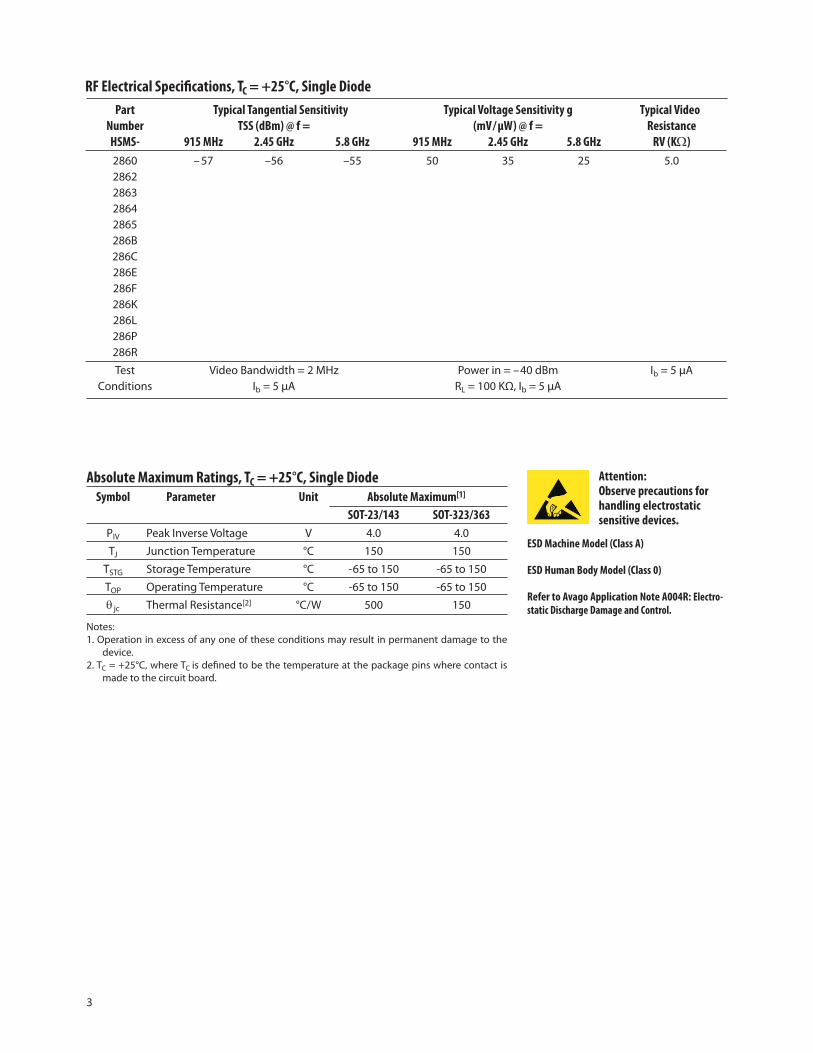
HSMS-286x Series Surface Mount Microwave Schottky Detector Diodes Data Sheet SOT-23 / SOT-143 Package Lead Code Identification (top view) Description Avago’s HSMS‑286x family of DC biased detector diodes have been designed and optimized for use from 915 MHz to 5.8 GHz. They are ideal for RF/ID and RF Tag applications as well as large signal detection, modulation, RF to DC conversion or voltage doubling. Available in various package configurations, this family of detector diodes provides low cost solutions to a wide variety of design problems. Avago’s manufacturing techniques assure that when two or more diodes are mounted into a single surface mount package, they are taken from adjacent sites on the wafer, assuring the highest possible degree of match. Pin Connections and Package Marking SOT-323 Package Lead Code Identification (top view) Notes: 1. Package marking provides orientation and identification. 2. The first two characters are the package marking code. The third character is the date code. Features • Surface Mount SOT‑23/SOT‑143 Packages • Miniature SOT‑323 and SOT‑363 Packages • High Detection Sensitivity: up to 50 mV/µW at 915 MHz up to 35 mV/µW at 2.45 GHz up to 25 mV/µW at 5.80 GHz • Low FIT (Failure in Time) Rate* • Tape and Reel Options Available • Unique Configurations in Surface Mount SOT‑363 Package – increase flexibility – save board space – reduce cost • HSMS‑286K Grounded Center Leads Provide up to 10 dB Higher Isolation • Matched Diodes for Consistent Performance • Better Thermal Conductivity for Higher Power Dissipation • Lead‑free * For more information see the Surface Mount Schottky Reliability Data Sheet. PLx 1 2 3 6 5 4 SOT-363 Package Lead Code Identification (top view) SERIES C SINGLE B 1 2 3 1 2 3 COMMON CATHODE F COMMON ANODE E 1 2 3 1 2 3 BRIDGE QUAD P UNCONNECTED TRIO L RING QUAD R 1 2 3 6 5 4 1 2 3 6 5 4 1 2 3 6 5 4 HIGH ISOLATION NCONNECTED PAIR K 1 2 3 6 5 4 COMMON CATHODE #4 UNCONNECTED PAIR #5 COMMON ANODE #3 SERIES #2 SINGLE #0 1 2 3 1 2 3 4 1 2 3 1 2 3 1 2 3
Transcript
HSMS-286x SeriesSurface Mount Microwave Schottky Detector Diodes
Data Sheet
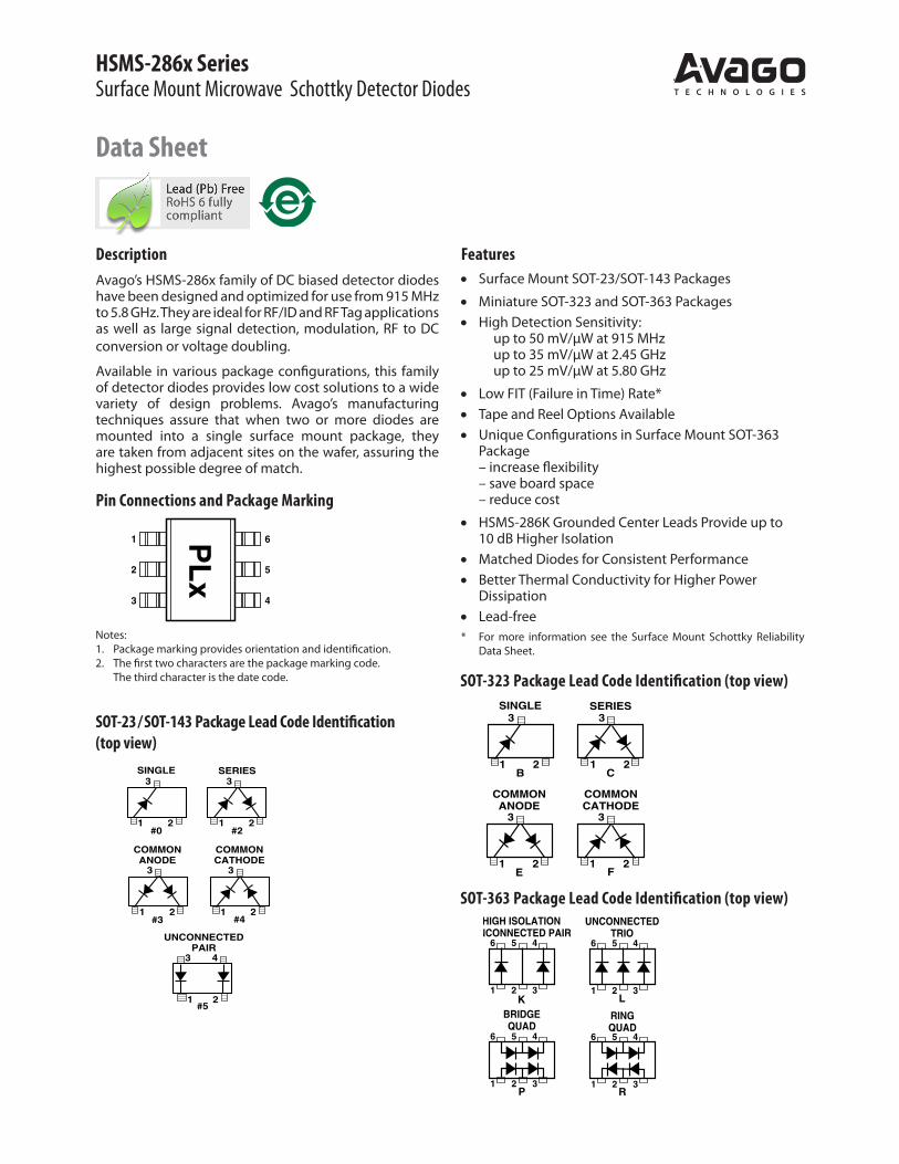
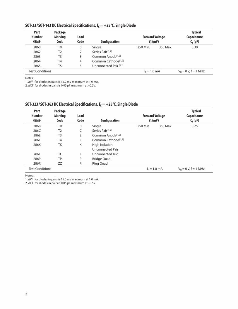
SOT-23/SOT-143 Package Lead Code Identification (top view)
DescriptionAvago’s HSMS‑286x family of DC biased detector diodes have been designed and optim ized for use from 915 MHz to 5.8 GHz. They are ideal for RF/ID and RF Tag applications as well as large signal detection, modulation, RF to DC conversion or voltage doubling.
Available in various package con figurations, this family of detector diodes provides low cost solutions to a wide variety of design problems. Avago’s manufacturing techniques assure that when two or more diodes are mounted into a single surface mount package, they are taken from adjacent sites on the wafer, assuring the highest possible degree of match.
Pin Connections and Package Marking
SOT-323 Package Lead Code Identification (top view)
Notes:1. Package marking provides orientation and identification.2. The first two characters are the package marking code.
The third character is the date code.
Features• Surface Mount SOT‑23/SOT‑143 Packages
• Miniature SOT‑323 and SOT‑363 Packages• High Detection Sensitivity:
up to 50 mV/µW at 915 MHz up to 35 mV/µW at 2.45 GHz up to 25 mV/µW at 5.80 GHz
• Low FIT (Failure in Time) Rate*• Tape and Reel Options Available• Unique Configurations in Surface Mount SOT‑363
Package – increase flexibility – save board space – reduce cost
• HSMS‑286K Grounded Center Leads Provide up to 10 dB Higher Isolation
• Matched Diodes for Consistent Performance• Better Thermal Conductivity for Higher Power
Dissipation• Lead‑free* For more information see the Surface Mount Schottky Reliability
Data Sheet.
PL
x
1
2
3
6
5
4
SOT-363 Package Lead Code Identification (top view)
SERIES
C
SINGLE
B1 2
3
1 2
3
COMMONCATHODE
F
COMMONANODE
E1 2
3
1 2
3
BRIDGEQUAD
P
UNCONNECTEDTRIO
L
RINGQUAD
R
1 2 3
6 5 4
1 2 3
6 5 4
1 2 3
6 5 4
HIGH ISOLATION UNCONNECTED PAIR
K1 2 3
6 5 4
COMMONCATHODE
#4
UNCONNECTEDPAIR
#5
COMMONANODE
#3
SERIES
#2
SINGLE
#01 2
3
1 2
3 4
1 2
3
1 2
3
1 2
3
2
SOT-23 / SOT-143 DC Electrical Specifications, TC = +25°C, Single Diode Part Package Typical Number Marking Lead Forward Voltage Capacitance HSMS- Code Code Configuration VF (mV) CT (pF) 2860 T0 0 Single 250 Min. 350 Max. 0.30 2862 T2 2 Series Pair [1,2] 2863 T3 3 Common Anode[1,2]
2864 T4 4 Common Cathode[1,2]
2865 T5 5 Unconnected Pair [1,2]
Test Conditions IF = 1.0 mA VR = 0 V, f = 1 MHz
Notes:1. ∆VF for diodes in pairs is 15.0 mV maximum at 1.0 mA.2. ∆CT for diodes in pairs is 0.05 pF maximum at –0.5V.
SOT-323 / SOT-363 DC Electrical Specifications, TC = +25°C, Single Diode Part Package Typical Number Marking Lead Forward Voltage Capacitance HSMS- Code Code Configuration VF (mV) CT (pF) 286B T0 B Single 250 Min. 350 Max. 0.25 286C T2 C Series Pair [1,2] 286E T3 E Common Anode[1,2]
286F T4 F Common Cathode[1,2]
286K TK K High Isolation Unconnected Pair 286L TL L Unconnected Trio 286P TP P Bridge Quad 286R ZZ R Ring Quad
Test Conditions IF = 1.0 mA VR = 0 V, f = 1 MHz
Notes:1. ∆VF for diodes in pairs is 15.0 mV maximum at 1.0 mA.2. ∆CT for diodes in pairs is 0.05 pF maximum at –0.5V.
3
RF Electrical Specifications, TC = +25°C, Single Diode Part Typical Tangential Sensitivity Typical Voltage Sensitivity g Typical Video Number TSS (dBm) @ f = (mV / µW) @ f = Resistance HSMS- 915 MHz 2.45 GHz 5.8 GHz 915 MHz 2.45 GHz 5.8 GHz RV (KΩ) 2860 – 57 –56 –55 50 35 25 5.0 2862 2863 2864 2865 286B 286C 286E 286F 286K 286L 286P 286R
Test Video Bandwidth = 2 MHz Power in = –40 dBm Ib = 5 µA Conditions Ib = 5 µA RL = 100 KΩ, Ib = 5 µA
Absolute Maximum Ratings, TC = +25°C, Single Diode Symbol Parameter Unit Absolute Maximum[1]
SOT-23/143 SOT-323/363 PIV Peak Inverse Voltage V 4.0 4.0
TJ Junction Temperature °C 150 150
TSTG Storage Temperature °C ‑65 to 150 ‑65 to 150
TOP Operating Temperature °C ‑65 to 150 ‑65 to 150
θ jc Thermal Resistance[2] °C/W 500 150
Notes:1. Operation in excess of any one of these conditions may result in permanent damage to the
device.2. TC = +25°C, where TC is defined to be the temperature at the package pins where contact is
made to the circuit board.
ESD Machine Model (Class A)
ESD Human Body Model (Class 0)
Refer to Avago Application Note A004R: Electro-static Discharge Damage and Control.
Attention: Observe precautions for handling electrostatic sensitive devices.
4
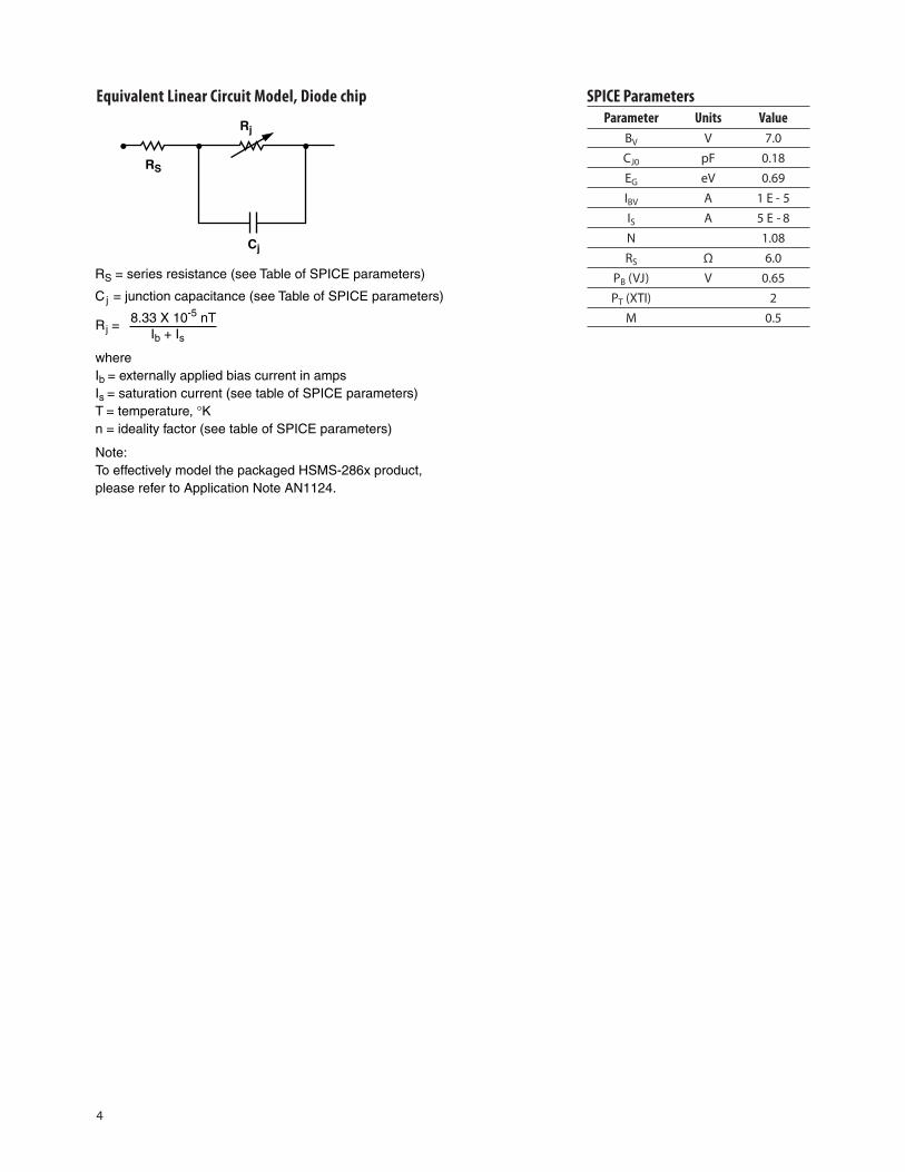
Equivalent Linear Circuit Model, Diode chip SPICE Parameters Parameter Units Value BV V 7.0
CJ0 pF 0.18
EG eV 0.69
IBV A 1 E ‑ 5
IS A 5 E ‑ 8
N 1.08
RS Ω 6.0
PB (VJ) V 0.65
PT (XTI) 2
M 0.5
Cj
Rj
RS
Rj = 8.33 X 10⁻⁵ nT
Ib + Is
whereIb = externally applied bias current in ampsIs = saturation current (see table of SPICE parameters)T = temperature, °Kn = ideality factor (see table of SPICE parameters)
Note:To effectively model the packaged HSMS-286x product, please refer to Application Note AN1124.
RS = series resistance (see Table of SPICE parameters)
Cj = junction capacitance (see Table of SPICE parameters)
5
Typical Parameters, Single Diode
1
10
100
1
10
FORW
ARD
VOLT
AGE
DIFF
EREN
CE(m
V)
VOLT
AGE O
UT (m
V)
POWER IN (dBm)
0.05 0.15 0.200.10 0.25
FORWARD VOLTAGE (V)
.01
.1
1
10
100
0.1 0.2 0.3 0.4 0. 70.6 0.8 0.90.5 1.0
FORW
ARD
CURR
ENT (
mA)
FORWARD VOLTAGE (V)
1
10
100
1000
10,000
–40 –30 –10 0–20 105
35
30
40
10
15
20
25
.1 1 1 0 100OU
TPUT
VOL
TAGE
(mV)
BIAS CURRENT (µA)
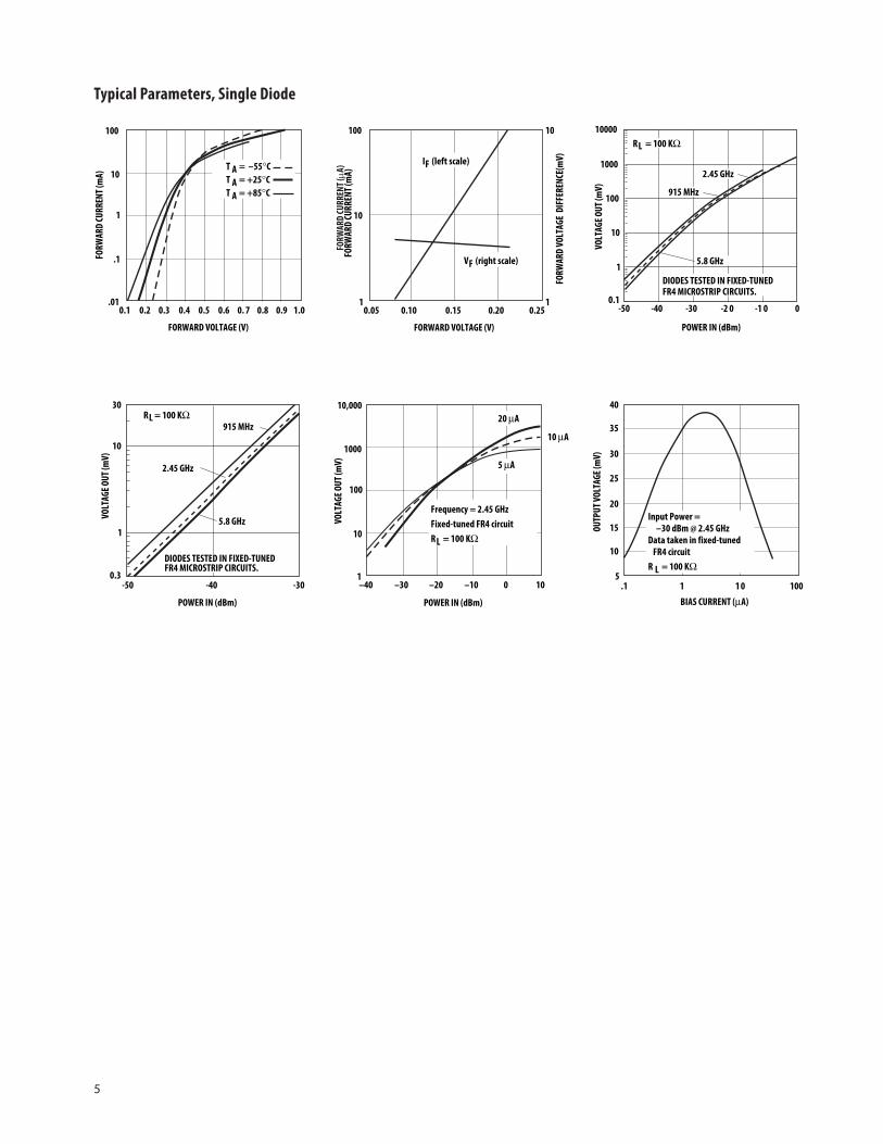
T A = –55°CT A = +25°CT A = +85°C
IF (left scale)
VF (right scale)
Frequency = 2.45 GHzFixed-tuned FR4 circuitRL = 100 KΩ
20 µA
5 µA
10 µA
Input Power = –30 dBm @ 2.45 GHzData taken in fixed-tuned FR4 circuitR L = 100 KΩ
VOLT
AGE O
UT (m
V)
-500.1
POWER IN (dBm)
-30 -2 0
10000
10
1
-40 0
100
-1 0
1000
RL = 100 KΩ
5.8 GHz
DIODES TESTED IN FIXED-TUNEDFR4 MICROSTRIP CIRCUITS.
915 MHz
2.45 GHz
VOLT
AGE O
UT (m
V)
-500.3
POWER IN (dBm)
-30
10
1
-40
30RL = 100 KΩ
2.45 GHz
915 MHz
5.8 GHz
DIODES TESTED IN FIXED-TUNEDFR4 MICROSTRIP CIRCUITS.
FORW
ARD
CURR
ENT (
mA)
FORW
ARD
CURR
ENT (mA
)
6
Appli cations Information
IntroductionAvago’s HSMS‑286x family of Schottky detector diodes has been developed specifically for low cost, high volume designs in two kinds of applications. In small signal detector applications (Pin < ‑20 dBm), this diode is used with DC bias at frequencies above 1.5 GHz. At lower frequencies, the zero bias HSMS‑285x family should be considered.
In large signal power or gain control applications (Pin> ‑20 dBm), this family is used without bias at frequencies above 4 GHz. At lower frequencies, the HSMS‑282x family is preferred.
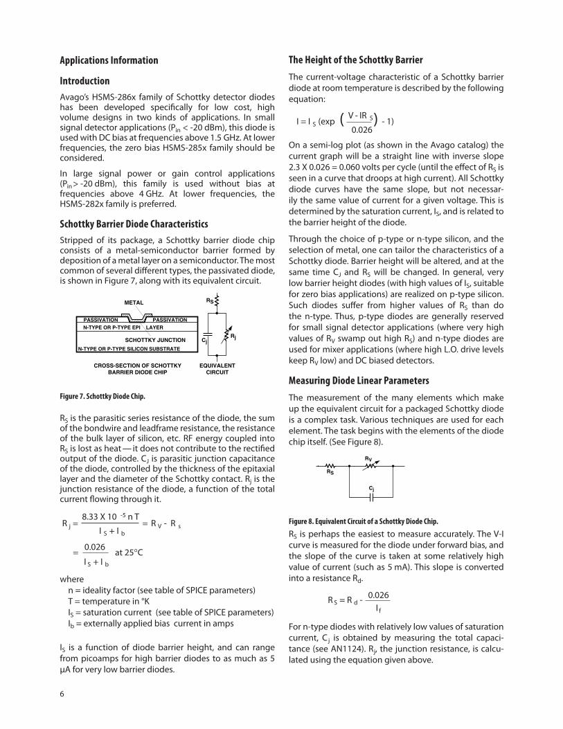
Schottky Barrier Diode CharacteristicsStripped of its package, a Schottky barrier diode chip consists of a metal‑semiconductor barrier formed by deposition of a metal layer on a semiconductor. The most common of several different types, the passivated diode, is shown in Figure 7, along with its equivalent circuit.
The Height of the Schottky Barrier
The current‑voltage character istic of a Schottky barrier diode at room temperature is described by the following equation:
HSMS-285A/6A fig 9
RS
RjCj
METAL
SCHOTTKY JUNCTION
PASSIVATION PASSIVATION
N-TYPE OR P-TYPE EPI LAYER
N-TYPE OR P-TYPE SILICON SUBSTRATE
CROSS-SECTION OF SCHOTTKYBARRIER DIODE CHIP
EQUIVALENTCIRCUIT
Figure 7. Schottky Diode Chip.
RS is the parasitic series resistance of the diode, the sum of the bondwire and leadframe resistance, the resistance of the bulk layer of silicon, etc. RF energy coupled into RS is lost as heat — it does not contribute to the rectified output of the diode. CJ is parasitic junction capaci tance of the diode, controlled by the thickness of the epitaxial layer and the diameter of the Schottky contact. Rj is the junction resistance of the diode, a function of the total current flowing through it.
RS
RV
Cj
Figure 8. Equivalent Circuit of a Schottky Diode Chip.
RS is perhaps the easiest to measure accurately. The V‑I curve is measured for the diode under forward bias, and the slope of the curve is taken at some relatively high value of current (such as 5 mA). This slope is converted into a resistance Rd.
8.33 X 10 -5 n TR j = = R V - R sI S + I b
0.026 = at 25°CI S + I b
V - IR SI = I S (exp ( ) - 1)0.026
8.33 X 10 -5 n TR j = = R V - R sI S + I b
0.026 = at 25°CI S + I b
V - IR SI = I S (exp ( ) - 1)0.026
where n = ideality factor (see table of SPICE parameters) T = temperature in °K IS = saturation current (see table of SPICE parameters)Ib = externally applied bias current in amps
IS is a function of diode barrier height, and can range from picoamps for high barrier diodes to as much as 5 µA for very low barrier diodes.
On a semi‑log plot (as shown in the Avago catalog) the current graph will be a straight line with inverse slope 2.3 X 0.026 = 0.060 volts per cycle (until the effect of RS is seen in a curve that droops at high current). All Schottky diode curves have the same slope, but not necessar‑ily the same value of current for a given voltage. This is deter mined by the saturation current, IS, and is related to the barrier height of the diode.
Through the choice of p‑type or n‑type silicon, and the selection of metal, one can tailor the characteristics of a Schottky diode. Barrier height will be altered, and at the same time CJ and RS will be changed. In general, very low barrier height diodes (with high values of IS, suitable for zero bias applica tions) are realized on p‑type silicon. Such diodes suffer from higher values of RS than do the n‑type. Thus, p‑type diodes are generally reserved for small signal detector applications (where very high values of RV swamp out high RS) and n‑type diodes are used for mixer applications (where high L.O. drive levels keep RV low) and DC biased detectors.
Measuring Diode Linear Parameters
The measurement of the many elements which make up the equivalent circuit for a pack aged Schottky diode is a complex task. Various techniques are used for each element. The task begins with the elements of the diode chip itself. (See Figure 8).
R V = R j + R S
0.026R S = R d - I f
For n‑type diodes with relatively low values of saturation current, Cj is obtained by measuring the total capaci‑tance (see AN1124). Rj, the junction resistance, is calcu‑lated using the equation given above.
7
The characterization of the surface mount package is too complex to describe here — linear equivalent circuits can be found in AN1124.
Detector Circuits (small signal)
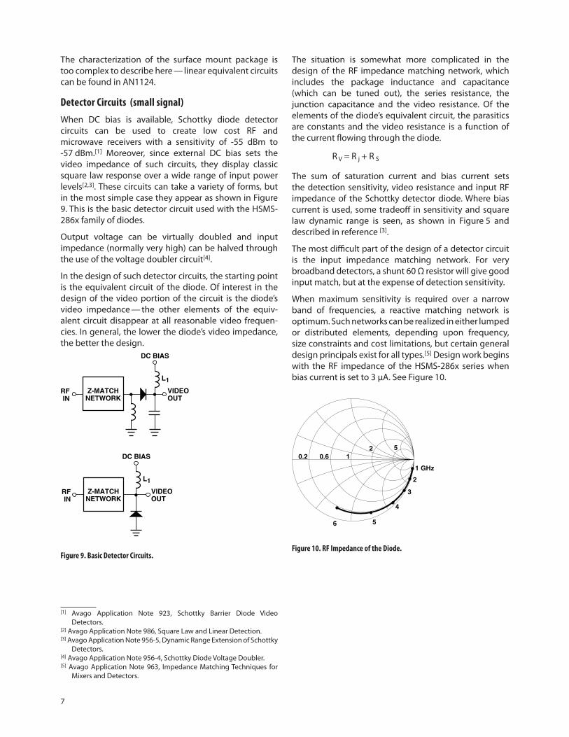
When DC bias is available, Schottky diode detector circuits can be used to create low cost RF and microwave receivers with a sensitivity of ‑55 dBm to ‑57 dBm.[1] Moreover, since external DC bias sets the video impedance of such circuits, they display classic square law response over a wide range of input power levels[2,3]. These circuits can take a variety of forms, but in the most simple case they appear as shown in Figure 9. This is the basic detector circuit used with the HSMS‑286x family of diodes.
Output voltage can be virtually doubled and input impedance (normally very high) can be halved through the use of the voltage doubler circuit[4].
In the design of such detector circuits, the starting point is the equivalent circuit of the diode. Of interest in the design of the video portion of the circuit is the diode’s video impedance — the other elements of the equiv‑alent circuit disappear at all reasonable video frequen‑cies. In general, the lower the diode’s video impedance, the better the design.
The situation is somewhat more complicated in the design of the RF impedance matching net work, which includes the pack age inductance and capacitance (which can be tuned out), the series resistance, the junction capacitance and the video resistance. Of the elements of the diode’s equiv alent circuit, the parasitics are constants and the video resistance is a function of the current flowing through the diode.
[1] Avago Application Note 923, Schottky Barrier Diode Video Detectors.
[2] Avago Application Note 986, Square Law and Linear Detection.[3] Avago Application Note 956‑5, Dynamic Range Extension of Schottky
Detectors.[4] Avago Application Note 956‑4, Schottky Diode Voltage Doubler.[5] Avago Application Note 963, Impedance Matching Techniques for
Mixers and Detectors.
HSMS-285A/6A fig 12
VIDEOOUT
RFIN
Z-MATCHNETWORK
L1
DC BIAS
VIDEOOUT
Z-MATCHNETWORK
L1
DC BIAS
RFIN
Figure 9. Basic Detector Circuits.
HSMS-285A/6A fig 13
1 GHz
2
3
4
56
0.2 0.6 12 5
Figure 10. RF Impedance of the Diode.
R V = R j + R S
0.026R S = R d - I f
The sum of saturation current and bias current sets the detection sensitivity, video resistance and input RF impedance of the Schottky detector diode. Where bias current is used, some tradeoff in sensitivity and square law dynamic range is seen, as shown in Figure 5 and described in reference [3].
The most difficult part of the design of a detector circuit is the input impedance matching network. For very broadband detectors, a shunt 60 Ω resistor will give good input match, but at the expense of detection sensitivity.
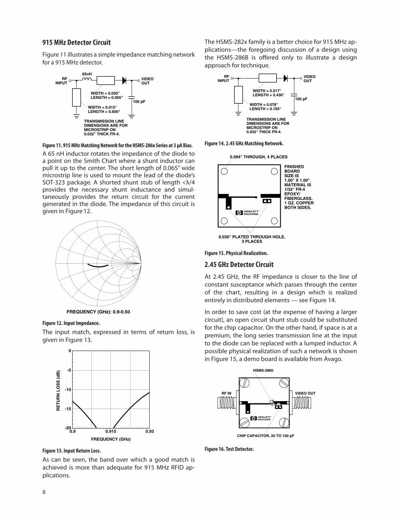
When maximum sensitivity is required over a narrow band of frequencies, a reactive matching network is optimum. Such net works can be realized in either lumped or distributed elements, depending upon frequency, size constraints and cost limitations, but certain general design principals exist for all types.[5] Design work begins with the RF impedance of the HSMS‑286x series when bias current is set to 3 µA. See Figure 10.
8
915 MHz Detector Circuit
Figure 11 illustrates a simple impedance matching network for a 915 MHz detector.
The HSMS‑282x family is a better choice for 915 MHz ap‑plications—the foregoing discussion of a design using the HSMS‑286B is offered only to illustrate a design approach for technique.
HSMS-285A/6A fig 14
65nH
100 pF
VIDEOOUT
RFINPUT
WIDTH = 0.050"LENGTH = 0.065"
WIDTH = 0.015"LENGTH = 0.600"
TRANSMISSION LINEDIMENSIONS ARE FORMICROSTRIP ON0.032" THICK FR-4.
HSMS-285A/6A fig 15
FREQUENCY (GHz): 0.9-0.93
HSMS-285A/6A fig 16
RE
TU
RN
LO
SS
(d
B)
0.9-20
FREQUENCY (GHz)
0.915
0
-10
-15
0.93
-5
100 pF
VIDEOOUT
RFINPUT
WIDTH = 0.017"LENGTH = 0.436"
WIDTH = 0.078"LENGTH = 0.165"
TRANSMISSION LINEDIMENSIONS ARE FORMICROSTRIP ON0.032" THICK FR-4.
0.030" PLATED THROUGH HOLE,3 PLACES
0.094" THROUGH, 4 PLACES
FINISHEDBOARDSIZE IS1.00" X 1.00". MATERIAL IS1/32" FR-4EPOXY/FIBERGLASS,1 OZ. COPPERBOTH SIDES.
HSMS-2860 fig 15
Figure 11. 915 MHz Matching Network for the HSMS-286x Series at 3 µA Bias.
A 65 nH inductor rotates the impedance of the diode to a point on the Smith Chart where a shunt inductor can pull it up to the center. The short length of 0.065” wide microstrip line is used to mount the lead of the diode’s SOT‑323 package. A shorted shunt stub of length <λ/4 provides the necessary shunt inductance and simul‑taneously provides the return circuit for the current generated in the diode. The impedance of this circuit is given in Figure 12.
Figure 12. Input Impedance.
The input match, expressed in terms of return loss, is given in Figure 13.
Figure 13. Input Return Loss.
As can be seen, the band over which a good match is achieved is more than adequate for 915 MHz RFID ap‑plications.
Figure 14. 2.45 GHz Matching Network.
Figure 15. Physical Realization.
2.45 GHz Detector Circuit
At 2.45 GHz, the RF impedance is closer to the line of constant susceptance which passes through the center of the chart, resulting in a design which is realized entirely in distributed elements — see Figure 14.
In order to save cost (at the expense of having a larger circuit), an open circuit shunt stub could be substituted for the chip capacitor. On the other hand, if space is at a premium, the long series transmission line at the input to the diode can be replaced with a lumped inductor. A possible physical realization of such a network is shown in Figure 15, a demo board is available from Avago.
CHIP CAPACITOR, 20 TO 100 pF
HSMS-2860
HSMS-285X fig 20 was 17
VIDEO OUTRF IN
Figure 16. Test Detector.
9
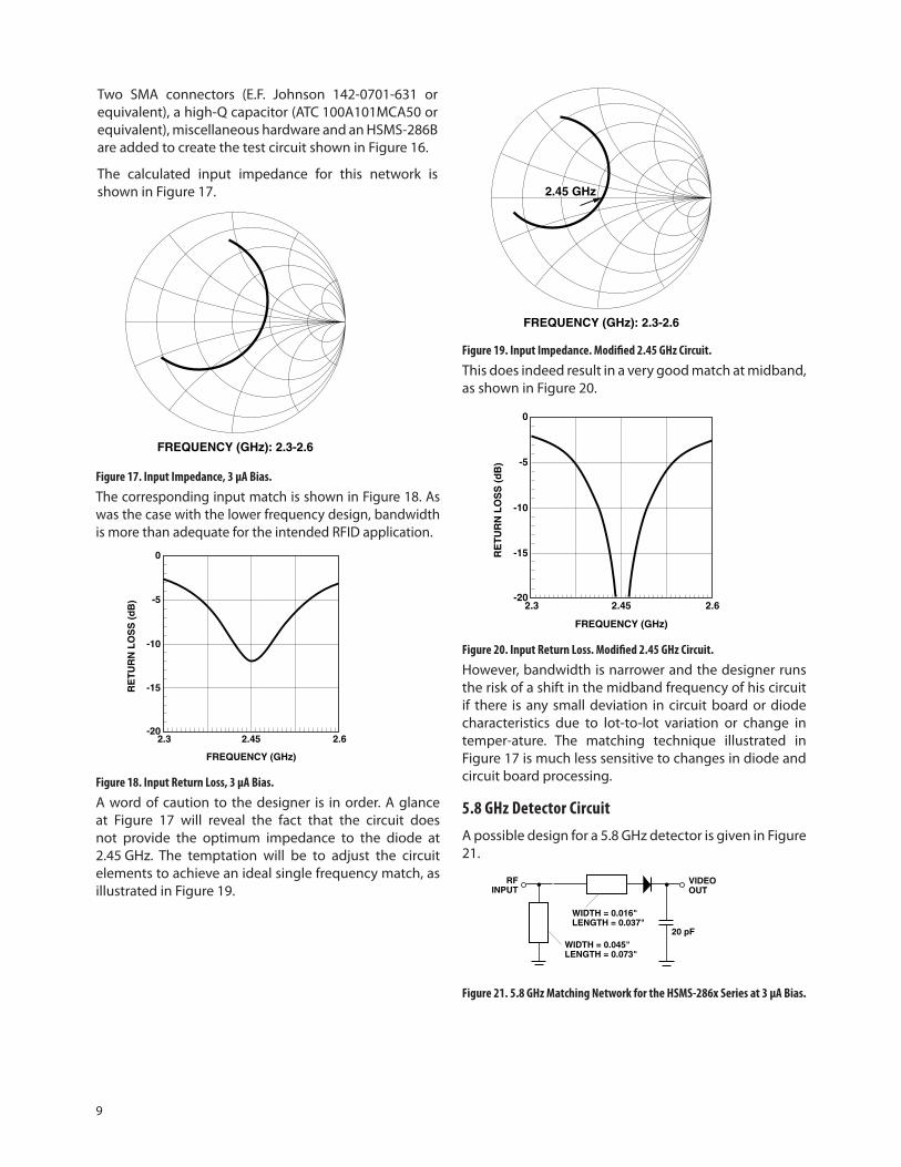
Two SMA connectors (E.F. Johnson 142‑0701‑631 or equivalent), a high‑Q capacitor (ATC 100A101MCA50 or equivalent), miscellaneous hardware and an HSMS‑286B are added to create the test circuit shown in Figure 16.
The calculated input impedance for this network is shown in Figure 17.
This does indeed result in a very good match at midband, as shown in Figure 20.
HSMS-0005 fig 21 was 18
FREQUENCY (GHz): 2.3-2.6
HSMS-285X fig 22 was 19
RE
TU
RN
LO
SS
(d
B)
2.3-20
FREQUENCY (GHz)
2.45
0
-10
-15
2.6
-5
HSMS-0005 fig 23 was 20
FREQUENCY (GHz): 2.3-2.6
2.45 GHz
HSMS-285X fig 24 was 21
RE
TU
RN
LO
SS
(d
B)
2.3-20
FREQUENCY (GHz)
2.45
0
-10
-15
2.6
-5
Figure 17. Input Impedance, 3 µA Bias.
The corresponding input match is shown in Figure 18. As was the case with the lower frequency design, bandwidth is more than adequate for the intended RFID application.
Figure 18. Input Return Loss, 3 µA Bias.
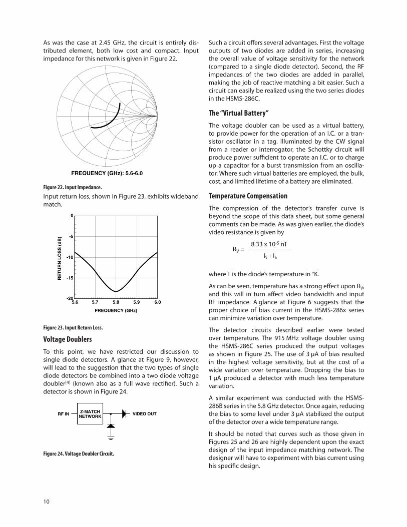
A word of caution to the designer is in order. A glance at Figure 17 will reveal the fact that the circuit does not provide the optimum impedance to the diode at 2.45 GHz. The temptation will be to adjust the circuit elements to achieve an ideal single frequency match, as illustrated in Figure 19.
However, bandwidth is narrower and the designer runs the risk of a shift in the mid band frequency of his circuit if there is any small deviation in circuit board or diode character istics due to lot‑to‑lot variation or change in temper‑ature. The matching technique illustrated in Figure 17 is much less sensitive to changes in diode and circuit board processing.
5.8 GHz Detector Circuit
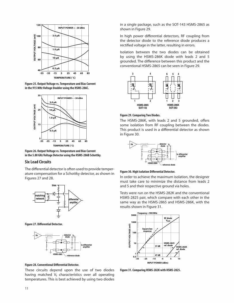
A possible design for a 5.8 GHz detector is given in Figure 21.
20 pF
VIDEOOUT
RFINPUT
WIDTH = 0.016"LENGTH = 0.037"
WIDTH = 0.045"LENGTH = 0.073"
TRANSMISSION LINEDIMENSIONS ARE FORMICROSTRIP ON0.032" THICK FR-4.
Figure 21. 5.8 GHz Matching Network for the HSMS-286x Series at 3 µA Bias.
10
As was the case at 2.45 GHz, the circuit is entirely dis‑tributed element, both low cost and compact. Input impedance for this network is given in Figure 22.
Such a circuit offers several advantages. First the voltage outputs of two diodes are added in series, increasing the overall value of voltage sensitivity for the network (compared to a single diode detector). Second, the RF impedances of the two diodes are added in parallel, making the job of reactive matching a bit easier. Such a circuit can easily be realized using the two series diodes in the HSMS‑286C.
The “Virtual Battery”
The voltage doubler can be used as a virtual battery, to provide power for the operation of an I.C. or a tran‑sistor oscillator in a tag. Illuminated by the CW signal from a reader or inter rogator, the Schottky circuit will produce power sufficient to operate an I.C. or to charge up a capacitor for a burst transmis sion from an oscilla‑tor. Where such virtual batteries are employed, the bulk, cost, and limited lifetime of a battery are eliminated.
Temperature Compensation
The compression of the detector’s transfer curve is beyond the scope of this data sheet, but some general comments can be made. As was given earlier, the diode’s video resistance is given by
8.33 x 10‑5 nT RV = IS + I b
where T is the diode’s temperature in °K.
As can be seen, temperature has a strong effect upon RV, and this will in turn affect video bandwidth and input RF impedance. A glance at Figure 6 suggests that the proper choice of bias current in the HSMS‑286x series can minimize variation over temperature.
The detector circuits described earlier were tested over temperature. The 915 MHz voltage doubler using the HSMS‑286C series produced the output voltages as shown in Figure 25. The use of 3 µA of bias resulted in the highest voltage sensitivity, but at the cost of a wide variation over temperature. Dropping the bias to 1 µA produced a detector with much less temperature variation.
A similar experiment was conducted with the HSMS‑286B series in the 5.8 GHz detector. Once again, reducing the bias to some level under 3 µA stabilized the output of the detector over a wide temperature range.
It should be noted that curves such as those given in Figures 25 and 26 are highly dependent upon the exact design of the input impedance matching network. The designer will have to experiment with bias current using his specific design.
HSMS-0005 fig 26 was 23
FREQUENCY (GHz): 5.6-6.0
HSMS-285X fig 27 was 24
RE
TU
RN
LO
SS
(d
B)
5.6-20
FREQUENCY (GHz)
5.8
0
-10
-15
6.0
-5
5.95.7
HSMS-285X fig 11 was 7
VIDEO OUTZ-MATCHNETWORKRF IN
Figure 22. Input Impedance.
Input return loss, shown in Figure 23, exhibits wideband match.
Figure 23. Input Return Loss.
Voltage Doublers
To this point, we have restricted our discus sion to single diode detectors. A glance at Figure 9, however, will lead to the suggestion that the two types of single diode detectors be combined into a two diode voltage doubler[4] (known also as a full wave rectifier). Such a detector is shown in Figure 24.
Figure 24. Voltage Doubler Circuit.
11
Figure 25. Output Voltage vs. Temperature and Bias Current in the 915 MHz Voltage Doubler using the HSMS-286C.
in a single package, such as the SOT‑143 HSMS‑2865 as shown in Figure 29.
In high power differential detectors, RF coupling from the detector diode to the reference diode produces a rectified voltage in the latter, resulting in errors.
Isolation between the two diodes can be obtained by using the HSMS‑286K diode with leads 2 and 5 grounded. The difference between this product and the conventional HSMS‑2865 can be seen in Figure 29.
-55 -35 -15 5 8545 65
OU
TPU
T V
OLT
AG
E (m
V)
TEMPERATURE (°C)
2540
80
60
120
100
INPUT POWER = –30 dBm
3.0 µA
1.0 µA
10 µA
0.5 µA
OU
TPU
T V
OLT
AG
E (m
V)
TEMPERATURE (°C)
5
15
35
25
INPUT POWER = –30 dBm
3.0 µA
10 µA
1.0 µA
0.5 µA
-55 -35 -15 5 8545 6525
matchingnetwork differential
amplifier
bias
to differentialamplifier
Vsdetectordiode
reference diode
PA
HSMS-2865
Figure 26. Output Voltage vs. Temperature and Bias Current in the 5.80 GHz Voltage Detector using the HSMS-286B Schottky.
Six Lead Circuits
The differential detector is often used to provide temper‑ature compensation for a Schottky detector, as shown in Figures 27 and 28.
Figure 27. Differential Detector.
Figure 28. Conventional Differential Detector.
These circuits depend upon the use of two diodes having matched Vf characteristics over all operating temperatures. This is best achieved by using two diodes
HSMS-2865SOT-143
HSMS-286KSOT-363
3 4 6 5 4
11 2 2 3
to differentialamplifier
Vsdetectordiode
reference diode
PA
HSMS-286K
-35 -25 -15 -5 155
37 dB
47 dB
OU
TPU
T V
OLT
AG
E (m
V)
INPUT POWER (dBm)
0.5
1000
100
10
1
5000Frequency = 900 MHz
HSMS-2825ref. diode
RF diodeVout
Square lawresponse
HSMS-282Kref. diode
Figure 29. Comparing Two Diodes.
The HSMS‑286K, with leads 2 and 5 grounded, offers some isolation from RF coupling between the diodes. This product is used in a differential detector as shown in Figure 30.
Figure 30. High Isolation Differential Detector.
In order to achieve the maximum isolation, the designer must take care to minimize the distance from leads 2 and 5 and their respective ground via holes.
Tests were run on the HSMS‑282K and the conventional HSMS‑2825 pair, which compare with each other in the same way as the HSMS‑2865 and HSMS‑286K, with the results shown in Figure 31.
Figure 31. Comparing HSMS-282K with HSMS-2825.
12
The line marked “RF diode, Vout” is the transfer curve for the detector diode — both the HSMS‑2825 and the HSMS‑282K exhibited the same output voltage. The data were taken over the 50 dB dynamic range shown. To the right is the output voltage (transfer) curve for the reference diode of the HSMS‑2825, showing 37 dB of isolation. To the right of that is the output voltage due to RF leakage for the reference diode of the HSMS‑282K, demonstrating 10 dB higher isolation than the conventional part.
Such differential detector circuits generally use single diode detectors, either series or shunt mounted diodes. The voltage doubler offers the advantage of twice the output voltage for a given input power. The two concepts can be combined into the differential voltage doubler, as shown in Figure 32.
PRF = RF power dissipated
Note that θjc, the thermal resistance from diode junction to the foot of the leads, is the sum of two component resistances,
matchingnetwork
bias
differentialamplifier
Figure 32. Differential Voltage Doubler, HSMS-286P.
Here, all four diodes of the HSMS‑286P are matched in their Vf characteristics, because they came from adjacent sites on the wafer. A similar circuit can be realized using the HSMS‑286R ring quad.
Other configurations of six lead Schottky products can be used to solve circuit design problems while saving space and cost.
Thermal Considerations
The obvious advantage of the SOT‑363 over the SOT‑143 is combination of smaller size and two extra leads. However, the copper leadframe in the SOT‑323 and SOT‑363 has a thermal conductivity four times higher than the Alloy 42 leadframe of the SOT‑23 and SOT‑143, which enables it to dissipate more power.
The maximum junction temperature for these three families of Schottky diodes is 150°C under all operating conditions. The following equation, equation 1, applies to the thermal analysis of diodes:
11600 (V f - I f R s)nTI f = I S e - 1
Equation (3).
2 1 1n - 4060 ( T - 298)
I s = I 0 ( T ) e 298
Equation (4).
T j = (V f I f + P RF ) θ jc + T a Equation (1).
θjc = θpkg + θchip Equation (2).
11600 (V f - I f R s)nTI f = I S e - 1
Equation (3).
2 1 1n - 4060 ( T - 298)
I s = I 0 ( T ) e 298
Equation (4).
T j = (V f I f + P RF ) θ jc + T a Equation (1).
θjc = θpkg + θchip Equation (2).
11600 (V f - I f R s)nTI f = I S e - 1
Equation (3).
2 1 1n - 4060 ( T - 298)
I s = I 0 ( T ) e 298
Equation (4).
T j = (V f I f + P RF ) θ jc + T a Equation (1).
θjc = θpkg + θchip Equation (2).
11600 (V f - I f R s)nTI f = I S e - 1
Equation (3).
2 1 1n - 4060 ( T - 298)
I s = I 0 ( T ) e 298
Equation (4).
T j = (V f I f + P RF ) θ jc + T a Equation (1).
θjc = θpkg + θchip Equation (2).
where
Tj = junction temperature
Ta = diode case temperature
θ jc = thermal resistance
Vf If = DC power dissipated
Package thermal resistance for the SOT‑323 and SOT‑363 package is approximately 100°C/W, and the chip thermal resistance for these three families of diodes is approxi‑mately 40°C/W. The designer will have to add in the thermal resistance from diode case to ambient — a poor choice of circuit board material or heat sink design can make this number very high.
Equation (1) would be straightforward to solve but for the fact that diode forward voltage is a function of temperature as well as forward current. The equation, equation 3, for Vf is:
where
n = ideality factor
T = temperature in °K
Rs = diode series resistance
and IS (diode saturation current) is given by
Equations (1) and (3) are solved simultaneously to obtain the value of junction temperature for given values of diode case temperature, DC power dissipation and RF power dissipation.
13
Diode Burnout
Any Schottky junction, be it an RF diode or the gate of a MESFET, is relatively delicate and can be burned out with excessive RF power. Many crystal video receivers used in RFID (tag) applications find themselves in poorly controlled environments where high power sources may be present. Examples are the areas around airport and FAA radars, nearby ham radio operators, the vicinity of a broadcast band transmitter, etc. In such environments, the Schottky diodes of the receiver can be protected by a device known as a limiter diode.[6] Formerly available only in radar warning receivers and other high cost electronic warfare applications, these diodes have been adapted to commercial and consumer circuits.
Avago offers a com plete line of surface mountable PIN limiter diodes. Most notably, our HSMP‑4820 (SOT‑23) or HSMP‑482B (SOT‑323) can act as a very fast (nano‑second) power‑sensitive switch when placed between the antenna and the Schottky diode, shorting out the RF circuit temporarily and reflecting the excessive RF energy back out the antenna.
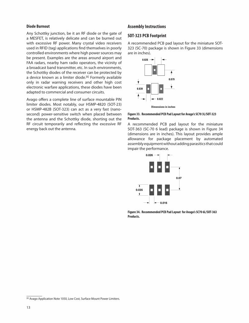
Figure 34. Recommended PCB Pad Layout for Avago’s SC70 6L/SOT-363 Products.
[6] Avago Application Note 1050, Low Cost, Surface Mount Power Limiters.
0.026
0.039
0.079
0.022
Dimensions in inches
0.026
0.075
0.016
0.035
Figure 33. Recommended PCB Pad Layout for Avago’s SC70 3L/SOT-323 Products.
A recommended PCB pad layout for the miniature SOT‑363 (SC‑70 6 lead) package is shown in Figure 34 (dimensions are in inches). This layout provides ample allowance for package placement by automated assembly equipment without adding parasitics that could impair the performance.
Assembly Instructions
SOT-323 PCB Footprint
A recommended PCB pad layout for the miniature SOT‑323 (SC‑70) package is shown in Figure 33 (dimensions are in inches).
14
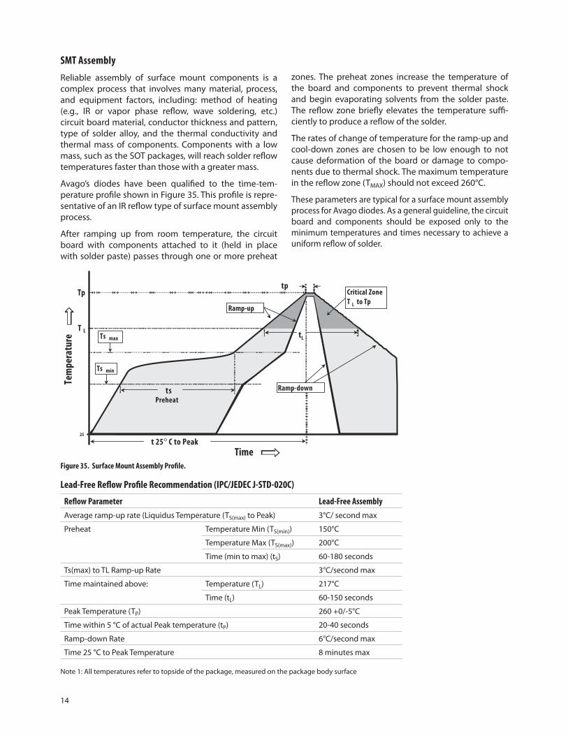
Figure 35. Surface Mount Assembly Profile.
SMT Assembly
Reliable assembly of surface mount components is a complex process that involves many material, process, and equipment factors, including: method of heating (e.g., IR or vapor phase reflow, wave soldering, etc.) circuit board material, conductor thickness and pattern, type of solder alloy, and the thermal conductivity and thermal mass of components. Components with a low mass, such as the SOT packages, will reach solder reflow temperatures faster than those with a greater mass.
Avago’s diodes have been qualified to the time‑tem‑perature profile shown in Figure 35. This profile is repre‑sentative of an IR reflow type of surface mount assembly process.
After ramping up from room temperature, the circuit board with components attached to it (held in place with solder paste) passes through one or more preheat
Average ramp‑up rate (Liquidus Temperature (TS(max) to Peak) 3°C/ second max
Preheat Temperature Min (TS(min)) 150°C
Temperature Max (TS(max)) 200°C
Time (min to max) (tS) 60‑180 seconds
Ts(max) to TL Ramp‑up Rate 3°C/second max
Time maintained above: Temperature (TL) 217°C
Time (tL) 60‑150 seconds
Peak Temperature (TP) 260 +0/‑5°C
Time within 5 °C of actual Peak temperature (tP) 20‑40 seconds
Ramp‑down Rate 6°C/second max
Time 25 °C to Peak Temperature 8 minutes max
Note 1: All temperatures refer to topside of the package, measured on the package body surface
zones. The preheat zones increase the temperature of the board and components to prevent thermal shock and begin evaporating solvents from the solder paste. The reflow zone briefly elevates the temperature suffi‑ciently to produce a reflow of the solder.
The rates of change of temperature for the ramp‑up and cool‑down zones are chosen to be low enough to not cause deformation of the board or damage to compo‑nents due to thermal shock. The maximum temperature in the reflow zone (TMAX) should not exceed 260°C.
These parameters are typical for a surface mount assembly process for Avago diodes. As a general guideline, the circuit board and components should be exposed only to the minimum temperatures and times necessary to achieve a uniform reflow of solder.