Implementation of a BPSK Transceiver for use with the University of Kansas Agile Radio by Ryan Reed Bachelor of Science, University of Kansas, Lawrence, Kansas, 2004 Submitted to the Department of Electrical Engineering and Computer Science and the Faculty of the Graduate School of the University of Kansas in partial fulfillment of the requirements for the degree of Master of Science in Electrical Engineering Thesis Committee ____________________________ Chairperson: Dr. Gary Minden ____________________________ Dr. David Petr ____________________________ Dr. Alexander Wyglinski Date Accepted: May 1, 2006
Transcript
Implementation of a BPSK Transceiver
for use with the University of Kansas Agile Radio
by
Ryan Reed
Bachelor of Science, University of Kansas, Lawrence, Kansas, 2004
Submitted to the Department of Electrical Engineering and Computer
Science and the Faculty of the Graduate School of the University of Kansas
in partial fulfillment of the requirements for the degree of Master of Science
in Electrical Engineering
Thesis Committee
____________________________Chairperson: Dr. Gary Minden
____________________________Dr. David Petr
____________________________Dr. Alexander Wyglinski
Date Accepted: May 1, 2006
ii
The Thesis Committee for Ryan Reed certifies
That this is the approved version of the following thesis:
Implementation of a BPSK Transceiver
In a Xilinx FPGA for use with KUAR
Committee:
_______________________Chairperson
_______________________
_______________________
Date approved: _______________________
iii
A designer knows he has achieved perfection not when there is nothing left to add, but when there is nothing left to take away.
- Antoine de Saint-Exupéry, Wind, Sand and Stars
iv
Abstract
The purpose of this study was to design a binary phase-shift-keying (BPSK)
transceiver specifically for use in the University of Kansas Agile Radio (KUAR). The
resulting transmitter communicates 1 Mbaud of data over a 5 MHz carrier, sampling at 80
Msps. The receiver compensates for frequency and phase errors presented by Doppler
shift and bit-time errors. Simulations show an error rate performance of 0.002835 at 10
dB of Eb/No. The resulting design could be used with other transceivers by making
slight alterations.
v
Acknowledgements
First, I’d like to thank Dr. Gary Minden, my advisor and mentor during my
graduate career at the University of Kansas. His ingenuity and guidance are so valuable
to everyone who works on the Flexible Wireless Systems for Rapid Network Evolution
project. I’d also like to thank Dr. Joseph Evans, who developed the proposal for this
project and received Grant AN-0230786 from the National Science Foundation.
Dr. Glenn Prescott, who was the first person to ignite my interest in engineering,
inspired me to learn more about digital signal processing and communication systems. It
was my pleasure to have him as an advisor during my undergraduate career.
Dr. David Petr showed me how to take signals and create communications
systems. Because of his teaching, I decided to become a communications engineer. His
creativity and inspiration both in the classroom and out were very encouraging to me.
I owe a very large thank you to Dr. Alex Wyglinski. His personality,
encouragement, and wisdom were inspiring. Our meetings were invaluable to my work.
I’d also like to thank Dr. Erik Perrins, who gave me a good starting point for my research.
My experiences as an undergraduate student at the University of Kansas showed
me the excellence of the program and helped me to appreciate the great opportunities that
this wonderful school provides to all of its students. I would like to thank the National
Science Foundation for funding Dr. Minden and the Flexible Wireless Systems for Rapid
Network Evolution Wireless Project.
Finally, thanks to my co-workers in the lab: Jordan Guffey, Ted Weidling, Rory
Petty, Leon Searl, Dan DePardo, Tim Newman, Brian Cordill, Levi Pierce, Megan
Lenherr, Rakesh Rajbanshi, Qi Chen, Anu Veeragandham, and Wes Mason who were
always helpful with the project. Thanks to my mom for her constant support and love;
vi
thanks to my dad for being a wonderful role model; thanks to my sister for bearing the
burden of older sibling; thanks to Jennifer for her support and assurance; and thanks to
Kodi, the greatest dog in the world.
vii
Table of Contents
Acceptance Page ............................................................................................................... ii
Quote ................................................................................................................................ iii
Abstract ............................................................................................................................ iv
Aknowledgements ............................................................................................................ v
CHAPTER 1 A BPSK TRANSCEIVER......................................................................... 1
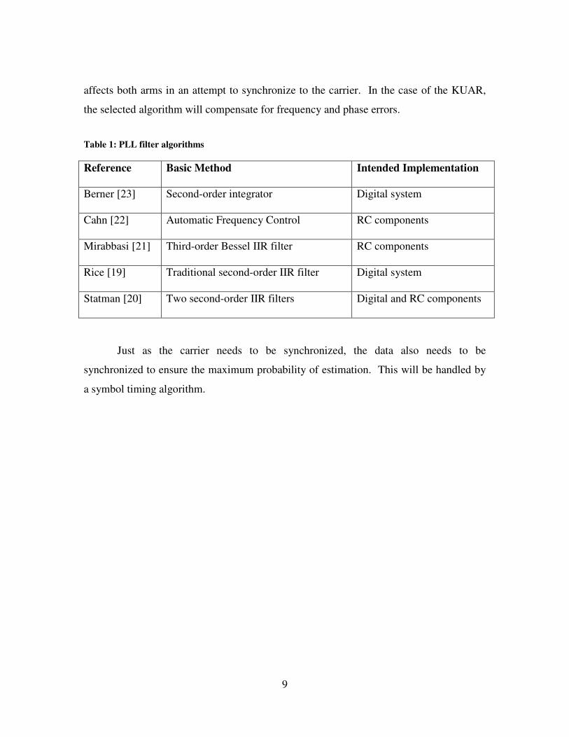
2.1 Overview of Implementations of Software-Defined Radios.................................... 72.2 Similar Work............................................................................................................ 82.3 Technologies for Synchronization ......................................................................... 112.4 Technologies for Bit-Time Recovery..................................................................... 14
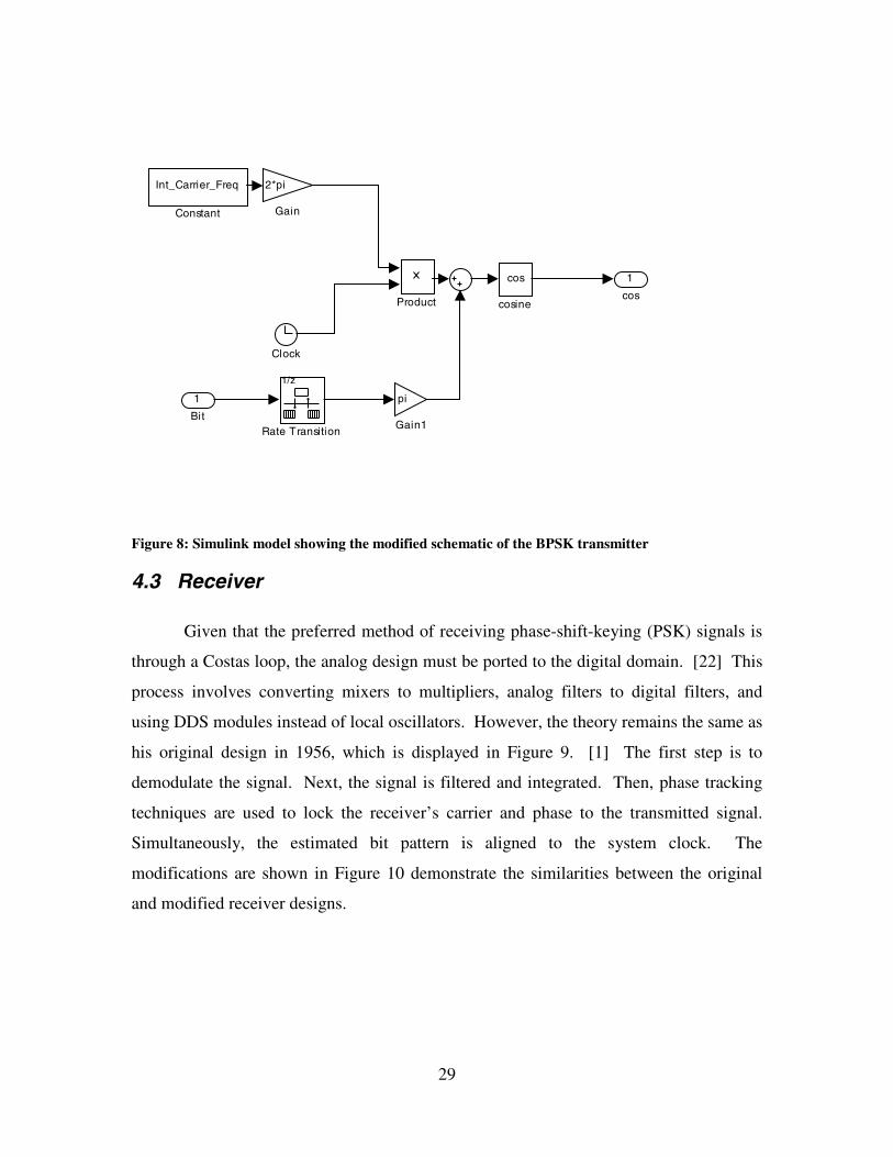
4.3.1 Receiver Overview and Scope of Problems ..................................................... 304.3.2 Details of the Matched Filter ........................................................................... 364.3.3 Frequency and phase tracking......................................................................... 38
The result of this multiplication rotates the input so that the phase and frequency
is steady with the constellation. This operation is necessary as both the loop and the
received lines are complex.
The in-phase result of this multiplication should resemble the transmitted bit
stream. The quad-phase result should be driven to zero by the loop filter.
4.3.3.2 Loop filter
This message signal passes into the loop filter, which determines how to rotate the
signal around the constellation. The loop filter is a second-order IIR filter, designed in
the traditional method. The traditional method provides an adequate response while
using few resources. Although a FIR is easier to design in the DSP world, it does not
have the same latency as that of an IIR filter with a comparable frequency response. For
example, a comparable FIR filter would require a substantially larger number of taps to
achieve the same degree of performance relative to this IIR filter. This excess of latency
drastically affects the ability of the loop. For instance, if one user moves suddenly and
stops, this creates a brief frequency deviation. If a FIR filter is used, this latency will
“update” the rotation significantly later than is necessary. Either this will allow an error
to pass through the system or it will modify a correct estimation to an incorrect value.
39
With only two orders, the IIR filter can update the loop significantly faster than the FIR
filter.
The traditional method is a second-order system because there are no third order
errors. A phase error is compensated with a first-order system; a frequency error is
compensated with a second-order system. This is described mathematically in Equations
10 and 11.
Equation 10: A phase error is corrected with a step response phase correction, which is a first-order system [19]
( )( ) ( )( )( ) ( )( )
ss
tut
tutAttA
θθθ
θωθω
∆=Θ∆=
∆+=+ 00 coscos
Equation 11: A frequency error is corrected with a ramp response frequency correction, which is a second-order system [19]
( )( ) ( ) ( )( )( ) ( ) ( )( )
2
00 coscos
ss
ttut
tttAtA
ωωθ
ωωωω
∆=Θ∆=
∆+=∆+
A PLL loop filter, designed in the traditional method, is described below, in
Figure 15.
40
Figure 15: Block diagram of a traditional PLL loop filter [19]
It can be shown that the phase error, Θe(s), for the step and ramp responses is
given by Equation 12. Furthermore, the boundary conditions of F(0) are also given in
Equation 12.
Equation 12: The phase error responses for a step and ramp, used to determine the boundary conditions [19]
( ) ( ) ( )( )
( ) ( ) ( )( ) ∞==
+∆=
+∆=Θ
≠=
+∆=
+∆=Θ
→
→
0if0
lim
00if0
lim
00
02
00
0
F
sFKKsssFKKs
s
F
sFKKs
s
sFKKss
ps
pe
ps
pe
ωω
θθ
A Proportional and Integrator filter, as described in Equation 13, fulfills the
boundary conditions, as ( ) ∞=0F .
F(s)Kp
s
K0
( )sΘ
( )sΘ̂
( ) ( ) ( )ssse Θ−Θ=Θ ˆ
E(s)
-
+
41
Equation 13: The response of a Proportional and Integrator filter [19]
( )s
KKsF 2
1 +=
Inserting the filter in the system gives the transfer function as follows in Equation
14.
Equation 14: Closed-loop transfer function of the PLL loop filter [19]
( ) ( )( )
( )( )
2
01
20
22
2
20102
2010
0
0
2
2
2
1
ˆ
K
KKK
KKK
ss
s
KKKsKKKs
KKKsKKK
s
sFKK
s
sFKK
s
ssH
p
pn
nn
nn
pp
pp
p
p
=
=
+++=++
+=+
=ΘΘ=
ζ
ω
ωζωωζω
Given the closed-loop transfer function, it can be shown that the equivalent noise
bandwidth of the loop is described by Equation 15.
Equation 15: Equivalent noise bandwidth of the closed-loop transfer function [19]
( ) ( )
+== ∫∞ ζζωωω4
1
20
1
0
2
2n
N djHH
B
The equivalent noise bandwidth of the filter is used to describe characteristics of
the loop, such as the pull-in range and acquisition time, which are described in Equations
16 and 17.
Equation 16: Pull-in range of the loop filter [19]
NBf 6≈∆
42
Equation 17: Acquisition time of the loop filter [19]
( )NN
LOCK BB
fT
3.14
3
2
+∆≈
Moving to the digital domain allows for the solution to the loop filter, given
design parameters. The solution equations are shown in Equation 18.
Equation 18: Solution equations for the digital loop filter [19]
( )
( )2
220
10
4
1
4
4
14
TBKKK
TBKKK
Np
Np
+=
+=
ζζ
ζζζ
The solution equations determine the filter coefficients given the design
parameters BN, Ts, and ζ. The final design parameter is given in Equation 19, where N is
the number of samples per symbol.
Equation 19: The final design parameter, the critical phase of the loop filter [19]
+=
ζζθ
4
1N
TBNn
Following the design procedure, the loop filter will be designed such that
0003125.0
025.0
20
10
==
KKK
KKK
p
p
Finally, the closed-form digital loop filter is solved in Equation 20.
43
Equation 20: The solution of the closed-loop digital filter [19]
( ) ( )( )
( )( ) ( )
21
21
210
1210
210
1210
21
025.00253125.0
12
1121
ˆ
−−−−
−−
−−
+−−=
−+
+−−−+=Θ
Θ=
zz
zz
zKKKzKKKK
zKKKzKKKK
z
zzH
pp
pp
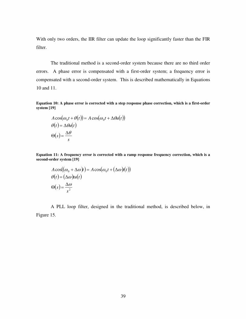
This output becomes the phase input to a DDS module. In effect, this translates
the exponential complex number to a trigonometric complex number. The entire loop is
shown in Figure 16.
Figure 16: Simulink model of the loop filter
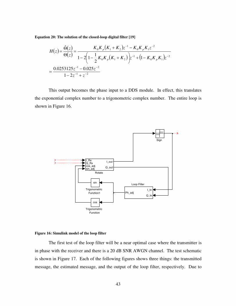
The first test of the loop filter will be a near optimal case where the transmitter is
in phase with the receiver and there is a 20 dB SNR AWGN channel. The test schematic
is shown in Figure 17. Each of the following figures shows three things: the transmitted
message, the estimated message, and the output of the loop filter, respectively. Due to
sin
TrigonometricFunction1
cos
TrigonometricFunction
Sign
I_RxQ_Rxcos_adjsin_adj
I_out
Q_out
Rotate
I_In
Q_InPh_adj
Loop Filter
44
the nature of BPSK, a unique symbol set will need to be transmitted in order to
differentiate between the phases. Thus, the second line in the results may be inverted
with respect to the transmitted signal.
Uniform RandomNumber
sin
TrigonometricFunction1
cos
TrigonometricFunction
Phase sin
Transmitter
DSP
Sine Wave3
DSP
Sine Wave2
Sign
Scope
round
RoundingFunction
I_RxQ_Rxcos_adjsin_adj
I_out
Q_out
Rotate
Product1
Product
I_In
Q_InPh_adj
Loop Filter
-1
Gain
80
Downsample1
80
Downsample
num(z)
80
Discrete Filter1
num(z)
80
Discrete Filter
AWGN
AWGNChannel
Figure 17: The test schematic for carrier synchronization
45
Figure 18: The ideal case for the loop filter
Figure 18 shows that the filter has compensated for the noise and shows that the
filter comes to steady state in about 10 µs. The next case will show how the filter reacts
to a constant phase misalignment in Figure 19.
46
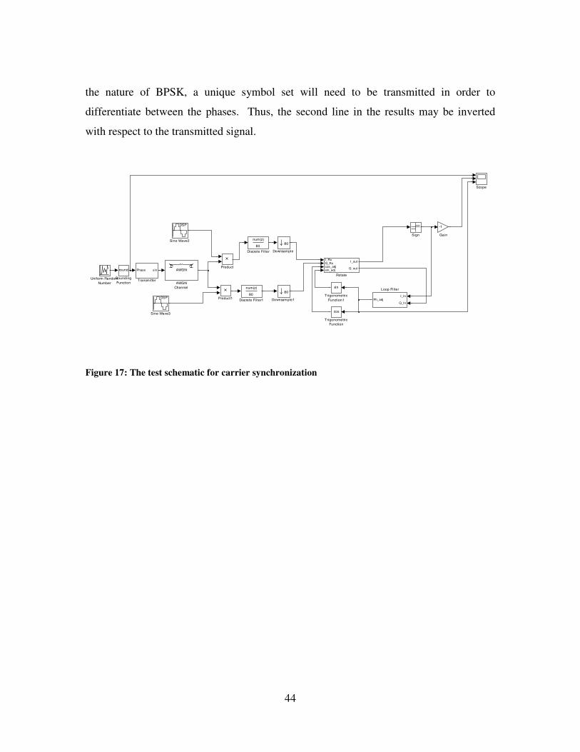
Figure 19: The loop filter’s response to a constant phase error
Once again, the filter compensates for the error within 10 µs. The next case
shows how the filter will react to a 20 Hz deviation. Figure 20 shows the expected, that
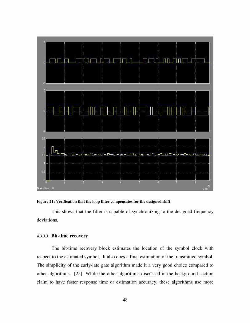
the output of the filter is a sloped line, while Figure 21 shows that the bits are correct and
that the error is compensated within 60 µs.
47
Figure 20: The loop filter’s response to a Doppler Shift
48
Figure 21: Verification that the loop filter compensates for the designed shift
This shows that the filter is capable of synchronizing to the designed frequency
deviations.
4.3.3.3 Bit-time recovery
The bit-time recovery block estimates the location of the symbol clock with
respect to the estimated symbol. It also does a final estimation of the transmitted symbol.
The simplicity of the early-late gate algorithm made it a very good choice compared to
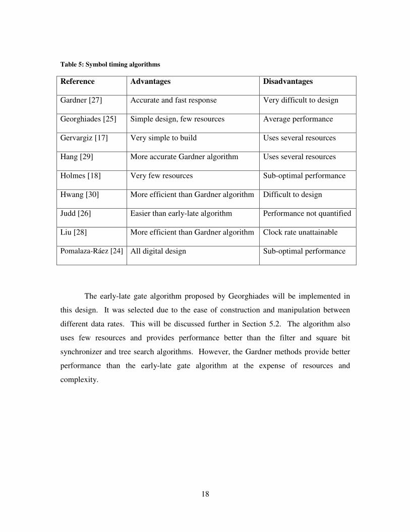
other algorithms. [25] While the other algorithms discussed in the background section
claim to have faster response time or estimation accuracy, these algorithms use more
49
resources. The tradeoff of resources to performance led to the determination that the
early-late gate algorithm is the best choice.
This algorithm uses another eighty-tap boxcar FIR filter to average over an
arbitrary bit interval. The result then splits into three branches: one has no delay, one has
one cycle of delay, and the final has two cycles of delay. In the middle of these three
branches is a latch, which gates based on the result of the next section. The final stage of
the three branches is the math, which determines both when to gate the latch and what the
bit estimate is. The slope of the input is determined by subtracting the top branch from
the lower branch. If the slope is zero, the clock is locked on the bit interval and the gate
will latch every eighty cycles. The center branch is multiplied by the slope to determine
if the slope is positive or negative. Thereby, the algorithm determines if the gate needs to
latch every seventy-nine or eighty-one cycles. The result appears as if the integration
window shifts towards the correct bit interval.
The center branch also serves as the bit estimate. Assuming the clock is locked,
the integration over the previous eighty samples provides the most accurate estimate of
the message. The downside of this algorithm is the lock time. If the transmitter and
receiver are one half bit-cycle off and the transmitted message is alternating on every bit,
it will take forty cycles to attain lock. If the message does not alternate on every bit, it
will take longer to lock. This does not mean that the bit estimate will be incorrect until
lock, but it will have little confidence. Although not coded, this is a possible output if
desired in the future. It would be preferable to have the algorithm output a locked line,
indicating if the algorithm is gating every eighty cycles.
This algorithm may be selected for implementation in software if space becomes
an issue. The advantage of performing this operation in logic is the parallel computation
versus the single thread of a microprocessor. However, since the algorithm runs
primarily at the symbol time, the fast speed of the microprocessor should be able to
handle this algorithm without diverting much from its other tasks. The Simulink model
50
of the Early-Late Gate algorithm is shown in Figure 22, and an example of an output is
shown in Figure 23.
z
1
Unit Delay2
z
1
Unit Delay1
z
1
Unit Delay Sign
Scope6
Early
Current
Late
Early Sample
Current Sample
Late Sample
Sampler
Correction Pulse
Sample T imer
RepeatingSequence
Product1
Product
uy
fcnEmbeddedMATLAB Function
num(z)
80
Discrete Fi lter
Figure 22: Simulink model of the Early-Late Gate bit recovery algorithm
51
Figure 23: An Early-Late Gate Algorithm locking to a signal
The results, seen in Figure 24, demonstrate that this receiver is capable of
estimating the message. Although other algorithms may realize a better SNR vs. bit-error
rate (BER) curve, that the novelty of this receiver is the implementation in an FPGA for a
mobile SDR.
With the combination of error-control and error-correction algorithms, the BER
performance should improve. These algorithms are proposed to run concurrently in the
FPGA’s embedded processor.
52
-2 0 2 4 6 8 10 1210
-7
10-6
10-5
10-4
10-3
10-2
10-1
100
Eb/No
BE
R
SNR vs. BER
Ideal
Simulated
Figure 24: Simulated SNR vs. BER for the BPSK Transceiver after carrier and bit synchronization.
53
CHAPTER 5 HARDWARE IMPLEMENTATION
5.1 Introduction
The previous simulation shows that the transceiver is capable of communicating a
message between the transmitter and receiver mathematically, and in simulation.
However, the transceiver needs to be built into firmware. The design is ported into
Xilinx ISE, a program that Xilinx sells for use with their FPGA processors. It provides
primarily three methods of creating designs to a user: programming in VHDL,
programming in Verilog, and programming through schematic. If the user chooses to
type code in the VHDL or Verilog languages, ISE will interpret this code and virtually
wire the processor to perform the algorithms. However, if the user chooses to draw the
algorithms in schematic format, the user will also have the option of coding in VHDL or
Verilog and produce modules that the schematic will interpret. The final schematic,
similarly, can be loaded in the FPGA processor. The design for KUAR was created in
schematic, and a few modules were designed in VHDL.
Since the simulation was created with as many simple blocks as possible, the port
to Xilinx ISE is nearly one to one. Xilinx provides the ability to create most digital and
math structures through their Intellectual Property Cores (IP Cores). These cores provide
the best optimization of selectable speed or resources, using the look-up table (LUT)-
based hardware in the Virtex-II Pro FPGA. Should a designer decide to not use an IP
Core, it would still be possible to create most algorithms from digital basics (e.g. Flip
Flops, logic gates, hardware multipliers, or block RAM) through a graphical schematic
approach, a programming VHDL approach, or a combination of the two.
Under these constraints, the Simulink design is ported to Xilinx ISE. In the
transition, mixers become multipliers, filters become delays, multipliers, and
accumulators, and delays become shift registers. Only two modules did not port easily in
54
this transition: the boxcar FIR filters and the IIR loop filter. The IP Core did not
efficiently build the boxcar FIR and there is no IP Core for an IIR filter.
Local oscillation is provided through a Direct Digital Synthesizer IP Core. This
module constructs sinusoids by use of LUT hardware. The DDS module’s size is
determined by the frequency accuracy and desired SFDR. The frequency is determined
through the pace at which the index increments through the LUT. Since these sinusoids
are created through LUT hardware, they also create a great deal of harmonic resonance.
This noise is counter-acted in one of two ways: Taylor Series Correction or Phase
Dithering. Taylor Series Correction is accomplished by using otherwise discarded bits in
an attempt to increase spurious-free dynamic range (SFDR). The result pushes the noise
floor very low, but leaves spectral harmonics throughout the working frequency range.
The Phase Dithering actually adds noise to the least significant bits in the phase slope.
The randomness thereby nearly eliminates harmonic components, but increases the noise
floor slightly. [31] Phase dithering was used in all local oscillators in this project as
harmonic interference is considered a bigger problem than noise floor. An example of
the GUI used to construct a DDS is shown in Figure 27.
Another component used in the simulation that does not port one-to-one is the
Boxcar Filter. Instead of using either of the Xilinx-provided FIR creation modules, this
filter was implemented more abstractly. Since the algorithm performs a non-weighted
moving average, only two modules are necessary. The two modules are an 80-tap shift
register and a block to perform the mathematical operations. This is discussed in greater
detail later in Section 5.2.
The final consideration is the switch from floating point in simulation to fixed
point in implementation. The data input to the FPGA comes from two analog-digital
converters running at a sampling frequency of 80 MSPS with a width of 14 bits. Thus,
all modules use at least 16 bits in an attempt to negate this problem. Sign extension and
truncation are used wherever necessary.
55
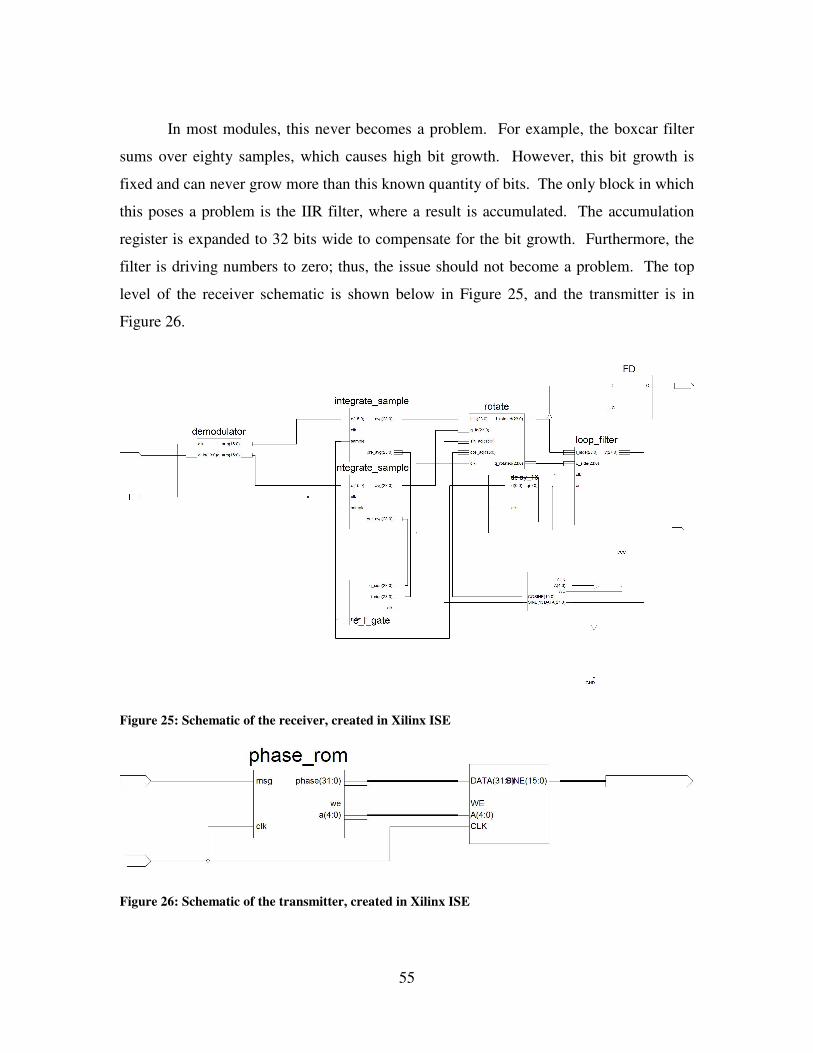
In most modules, this never becomes a problem. For example, the boxcar filter
sums over eighty samples, which causes high bit growth. However, this bit growth is
fixed and can never grow more than this known quantity of bits. The only block in which
this poses a problem is the IIR filter, where a result is accumulated. The accumulation
register is expanded to 32 bits wide to compensate for the bit growth. Furthermore, the
filter is driving numbers to zero; thus, the issue should not become a problem. The top
level of the receiver schematic is shown below in Figure 25, and the transmitter is in
Figure 26.
Figure 25: Schematic of the receiver, created in Xilinx ISE
Figure 26: Schematic of the transmitter, created in Xilinx ISE
56
Figure 27: Xilinx IP Core used to create a DDS for use as a local oscillator
5.2 Boxcar filter implementation
Several different designs for the boxcar filter module were explored before the
final design was selected. The goal was not only to perform the operations necessary to
the algorithm, but also to minimize the consumption of the FPGA resources. The first
method of designing this filter was to use one of the Xilinx FIR IP Cores. This process
included telling the core GUI how many taps to include, 80 in this case; what bit
resolution to use (16 in this case), the symmetry of the taps (symmetric), whether the bits
are signed or unsigned (signed), and if the coefficients need to be reloaded at any point
(false). Following this procedure, and loading the coefficients (eighty ones) into the core,
the core generates a filter, designed in Direct Form, which performs the desired
57
operation. The problem with this algorithm is the overuse of FPGA resources. Instead of
eliminating the multipliers it used forty multipliers. Due to the coefficient’s symmetry,
multipliers can be reused. Finally, since adders only have two inputs, this design will use
several in hierarchy to produce a result.
The next implementation involved using an adder, a subtractor, and several flip
flops. The input split as one input into the adder and the input into a chain of 79 flip
flops. The adder result was stored into a single flip flop. This flip flop output provided
the second input to the adder; thus, incoming samples are accumulated. Only 79 flip
flops were necessary on the flip flop chain due to the delay through the math chain. This
caused the eightieth sample to reach the subtractor at the same time as the input. The
output of the flip flop chain was subtracted from the math chain flip flop. This reduced
the resource consumption compared to the FIR IP Core. However, now, the algorithm
was incorrect. Since the single flip flop in the math chain is before the subtractor, this
flip flop will overflow if the input is not alternating ones and zeros. Furthermore, shift
registers consume fewer resources than flip flops, allowing for one more size
optimization.
The final and best algorithm replaces the flip flop chain with an 80-length, 16-
deep shift register. Inputs are stored here and pass into the math block after 80 cycles.
The shift register can also be configured for variable length. This is an advantage for
flexibility as the ratio of sampling rate to symbol rate determines the integration period.
Thus, the boxcar filters can be reused for different M-ary PSK designs.
Instead of using IP Cores to build the necessary adders and subtractors, the same
operation can be performed in two lines of VHDL code. First, a signal is instantiated to
zero to serve as the memory register. Secondly, the math is performed and, the result is
assigned to the output. This code serves the same purpose as blocks designed to add and
subtract. The result is the sum of the previous eighty input samples on every clock cycle.
The same design techniques are used on the boxcar filter in the early-late-gate operation.
58
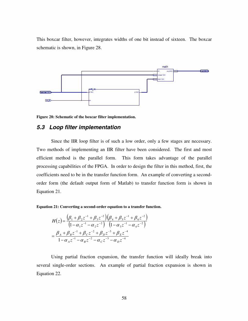
This boxcar filter, however, integrates widths of one bit instead of sixteen. The boxcar
schematic is shown, in Figure 28.
Figure 28: Schematic of the boxcar filter implementation.
5.3 Loop filter implementation
Since the IIR loop filter is of such a low order, only a few stages are necessary.
Two methods of implementing an IIR filter have been considered. The first and most
efficient method is the parallel form. This form takes advantage of the parallel
processing capabilities of the FPGA. In order to design the filter in this method, first, the
coefficients need to be in the transfer function form. An example of converting a second-
order form (the default output form of Matlab) to transfer function form is shown in
Equation 21.
Equation 21: Converting a second-order equation to a transfer function.
( ) ( )( ) ( )( )4321
4321
24
13
26
154
22
11
23
121
1
11
−−−−
−−−−
−−
−−
−−
−−
−−−−++++=
−−++
−−++=
zzzz
zzzz
zz
zz
zz
zzzH
DCBA
EDCBA
ααααβββββ
ααβββ
ααβββ
Using partial fraction expansion, the transfer function will ideally break into
several single-order sections. An example of partial fraction expansion is shown in
Equation 22.
59
Equation 22: An example of using partial fraction expansion on a transfer function.
( )
13
31
2
21
1
11
0
00
4321
4321
1111
1
−−−−
−−−−−−−−
−+−+−+−+=−−−−
++++=
zp
r
zp
r
zp
r
zp
rk
zzzz
zzzzzH
DCBA
EDCBA
ααααβββββ
This would be the ideal structure for any IIR implemented in an FPGA if the
partial fraction expansion yields single-order sections. It is ideal because the entire
operation could be performed in one cycle. However, with the coefficients used in this
design, the expansion yields a double pole equation, thereby nullifying the reason for
choosing this structure, as the algorithm would take more than one cycle. The
implementation of the filter in this design would yield one branch with a single-order
section and one with a second-order section. This is shown in Equation 23.
Equation 23: The result of using partial fraction expansion on a system with a double pole.
( ) ( )210
11
0
00
11 −− −+−+=zp
r
zp
rkzH
The final structure explored in this research is Biquad Direct Form II Transposed.
In this form, the second-order structure is used to create the filter. This structure has
more latency than the parallel form; however, timing is met since the data rate is equal to
the symbol rate, which is much slower than the clock rate. Therefore, several operations
can be performed before the result must be known. This schematic is shown in Figure
29.
60
Figure 29: Schematic of the loop filter implemented in single-order cascaded form.
The block labeled sign performs the initial operation of multiplying the quad-
phase line by the sign of the in-phase line. The next block, labeled “feedback_add,”
performs the second-order feedback operations. The result is fed into both itself and a
delay block such that the result is ( )2121
1−− +−=
zzzH fb . The result of this operation is
passed into the feed-forward loop to perform the operations in the numerator. Therefore,
the result is the desired ( )21
21
21
025.00253125.0−−
−−
+−−=
zz
zzzH .
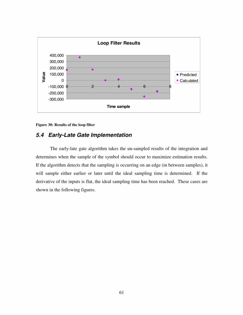
Results are shown below in Figure 30. The output of the filter algorithm differs
from the predicted output typically by 1 due to rounding error.
61
Loop Filter Results
-300,000
-200,000
-100,000
0
100,000
200,000
300,000
400,000
0 2 4 6 8
Time sample
Val
ue Predicted
Calculated
Figure 30: Results of the loop filter
5.4 Early-Late Gate Implementation
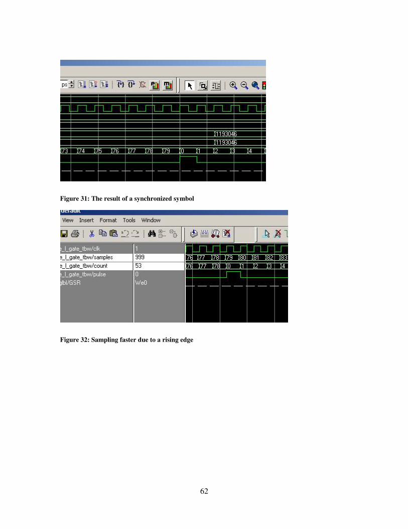
The early-late gate algorithm takes the un-sampled results of the integration and
determines when the sample of the symbol should occur to maximize estimation results.
If the algorithm detects that the sampling is occurring on an edge (in between samples), it
will sample either earlier or later until the ideal sampling time is determined. If the
derivative of the inputs is flat, the ideal sampling time has been reached. These cases are
shown in the following figures.
62
Figure 31: The result of a synchronized symbol
Figure 32: Sampling faster due to a rising edge
63
Figure 33: Sampling slower due to a falling edge
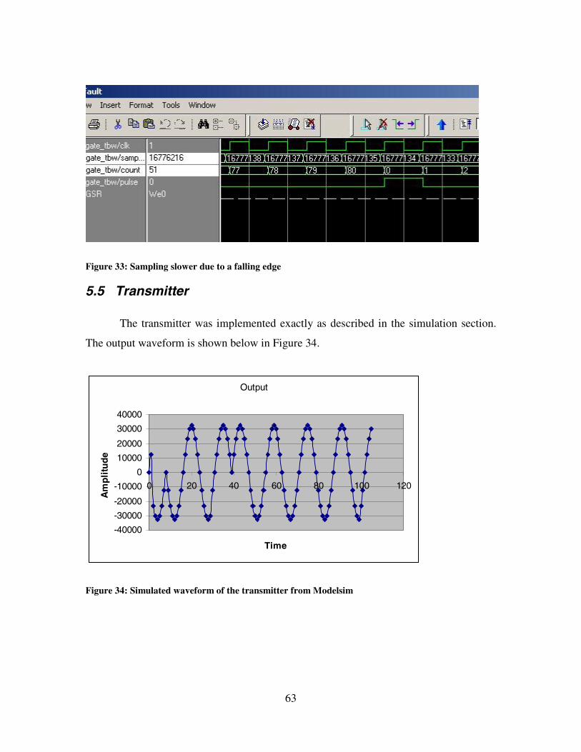
5.5 Transmitter
The transmitter was implemented exactly as described in the simulation section.
The output waveform is shown below in Figure 34.
Output
-40000
-30000
-20000
-10000
0
10000
20000
30000
40000
0 20 40 60 80 100 120
Time
Am
pli
tud
e
Figure 34: Simulated waveform of the transmitter from Modelsim
64
CHAPTER 6 CONCLUSION
The results shown above validate that the firmware implementation is a precise
realization of the computer simulation. Given that all the components of the firmware
match those of the simulations, the SNR vs. BER curve should also meet those of the
simulation. A sample simulation of the entire receiver is in Figure 35, showing that the
output is the estimate and a pulse dictating that the estimate is complete.
Figure 35: Sample simulation of the receiver
The thesis proposes larger algorithms which should provide better performance.
It also demonstrates means of using this design as the basis of M-PSK transceivers. The
transceiver is capable of communicating 1 Mbaud of data at the provided SNR vs. BER
ratio. Finally, the selected algorithms provide an adequate means of solving for
frequency, phase, and bit-time errors.
Algorithms were chosen such that errors are reduced while maintaining resource
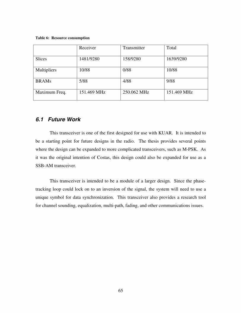
efficiency. The resource consumption by the receiver and transmitter is shown in Table
6.
65
Table 6: Resource consumption
Receiver Transmitter Total
Slices 1481/9280 158/9280 1639/9280
Multipliers 10/88 0/88 10/88
BRAMs 5/88 4/88 9/88
Maximum Freq. 151.469 MHz 250.062 MHz 151.469 MHz
6.1 Future Work
This transceiver is one of the first designed for use with KUAR. It is intended to
be a starting point for future designs in the radio. The thesis provides several points
where the design can be expanded to more complicated transceivers, such as M-PSK. As
it was the original intention of Costas, this design could also be expanded for use as a
SSB-AM transceiver.
This transceiver is intended to be a module of a larger design. Since the phase-
tracking loop could lock on to an inversion of the signal, the system will need to use a
unique symbol for data synchronization. This transceiver also provides a research tool
for channel sounding, equalization, multi-path, fading, and other communications issues.
66
CHAPTER 7 REFERENCES
[1] J. Costas, “Synchronous Communications,” Proceedings of the IEEE, vol. 44, p. 1713-1718, 1956.
[2] Spectrum Policy Task Force, “Spectrum Policy Task Force Report ET Docket No. 02-135,” U. S. Federal Communications Commission, 2002.
[3] J. Mitola, “Cognitive Radio for Flexible Mobile Multimedia Communications,” in IEEE International Workshop on Mobile Multimedia Communications, 1999, p. 3-10.
[4] F. Weidling, D. Datla, V. Petty, P. Krishnan, and G. J. Minden, “A Framework for R.F. Spectrum Measurements and Analysis,” in Proceedings of IEEE Dynamic Spectrum Access Networks 2005, Baltimore, Maryland, 2005.
[5] DARPA XG Working Group, “XG Policy Language Framework, Request for Comments,” version 1.0, prepared by BBN Technologies, Cambridge, Massacusetts, USA, April 2004.
[6] C. Serra, “SDR Forum,” 2006, http://www.sdrforum.org/.
[7] G. J. Minden, “KU Agile Radio Overview,” technical report, University of Kansas, Lawrence, Kansas, 2005.
[8] C. Dick, “The Platform FPGA: Enabling the Software Radio,” in Proceedings of the2002 Software Defined Radio Technical Conference and Product Exposition,2002.
[9] J. Mitola, “Software Radios Survey, Critical Evaluation and Future Decisions,” IEEE Aerospace and Electronic Systems Magazine, vol. 8 p. 25-36, 1993.
[10] BEE Home Page, Berkeley Wireless Research Center, University of California, Berkeley, 2006, http://bwrc.eecs.berkeley.edu/Research/BEE/.
[11] J. Steinheider, V. Lum, J. Santos, “Field Trials of an All-Software GSM Basestation,” Vanu, Inc, 2003.
[12] A. Chiu and J. Forbess, “A Handheld Software Radio Based on the iPAQ PDA: Software,” in Proceedings of the 2003 Software Defined Radio Technical Conference, 2003.
[13] J. Forbess and M. Wormley, “A Handheld Software Radio Based on the iPAQ PDA: Hardware,” in Proceedings of the 2003 Software Defined Radio Technical Conference, 2003.
67
[14] B. Massey, NWACC/PSU SDR, “WebHome – sdr,” 2006, http://wiki.cs.pdx.edu/~sdr/.
[15] “SDR-3000 Series Software Defined Radio Transceiver Platform,” Spectrum Signal Processing, 2005.
[16] “JTRS SDR Kit,” ISR Technologies, 2006.
[17] J. Gevargiz, “Performance Analysis of an all Digital BPSK Demodulator,” in Proceedings of IEEE Global Telecommunications Conference, vol. 3, p. 1670-1676, 1993.
[18] J. Holmes, “Tracking Performance of the Filter and Square Bit Synchronizer,” IEEE Transactions on Communications, vol. 28 (8), p. 1154-1158, 1980.
[19] M. Rice, “Introduction to Digital Communication Theory,” 2004, http://www.ee.byu.edu/class/ee485public/ee485.fall.04/.
[20] J. Statman and W. Hurd, “An Estimator-Predictor Approach to PLL Loop Filter Design,” IEEE Transactions on Communications, vol. 38 (10), p. 1667-1669, 1990.
[21] S. Mirabbasi, and K. Martin, “Design of Loop Filter in Phase-Locked Loops,” IEEE Electronics Letters, vol. 35 (21), p. 1801-1802, 1999.
[22] C. Cahn, “Improving Frequency Acquisition of a Costas Loop,” IEEE Transactions on Communications, vol. 25 (12), p. 1453-1459, 1977.
[23] J. Berner, J. Layland and P. Kinman, “Flexible Loop Filter Design for Spacecraft Phase-Locked Receivers,” IEEE Transactions on Aerospace and Electronic Systems, vol. 37 (3), p. 957-964, 2001.
[24] C. Pomalaza-Ráez and S. Mohan, “Application of Tree Search Algorithms to Bit Synchronization,” in Proceedings of the 33rd Midwest Symposium on Circuits and Systems, vol. 2, p. 1026-1029, 1991.
[25] C. Georghiades, “Synchronization,” The Communications Handbook, 2nd ed., Ed. J. Gibson, Boca Raton: CRC Press, 2002.
[26] D. Judd, “Data Synchronization Simulation Using the Mathworks Communications Toolbox,” IEEE International Conference on Communications, vol. 2, p. 706-710, 1996.
68
[27] F. Gardner, “Interpolation in Digital Modems – Part I: Fundamentals,” IEEE Transactions on Communications, vol. 41 (3), p. 501-507, 1993.
[28] X. Liu and A. Willson, “An New Interpolated Symbol Timing Recovery Method,” IEEE International Symposium on Circuits and Systems, vol. 2, p. 569-572, 2004.
[29] Z. Hang and M. Renfors, “A New Symbol Synchronizer with Reduced Timing Jitter for QAM Systems,” in Proceedings of the IEEE Global Telecommunications Conference, vol. 2, p. 1292-1296, 1995.
[30] J. Hwang and C. Chu, “FPGA Implementation of an All-Digital T/2-Spaced QPSK Receiver with Farrow Interpolation Timing Synchronizer and Recursive Costas Loop,” Proceedings of 2004 IEEE Asia-Pacific Conference on Advanced System Integrated Circuits, p. 248-251, 2004.
[31] Xilinx LogiCore, “Direct Digital Synthesizer, v. 5.0,” Xilinx, DS246, Apr. 2005.
[32] D. DePardo, “5 GHz Block Diagram,” technical report, University of Kansas: Agile Radio Project, Lawrence, Kansas, 2005.
[33] L. Searl, “Radio Digital Board Assembly Bottom,” technical report, University of Kansas: Agile Radio Project, Lawrence, Kansas, 2005.
[35] K. Shanmugan and A. Breipohl, Random Signals: Detection, Estimation and Data Analysis, New York: Wiley, 1988.
[36] C. Bergstrom, S. Chuprun, S. Gifford and G. Maalouli, “Software Defined Radio (SDR) Special Military Applications,” in Proceedings of the IEEE Military Communications Conference, vol. 1, p. 383-388, 1988.
[37] S. Blust, “Modular Multifunction Information Transfer System Forum on Sofware Defined Radio,” 1998, in Proceedings of the 8th Annual International Symposium on Advanced Radio Technologies,http://www.its.bldrdoc.gov/isart/art98/slides98/blust /blus_s_all.pdf.
[38] S. Blust, “Software Based Radio,” Software Defined Radio, Ed. W. Tuttlebee, West Sussex: John Wiley & Sons, Ltd., 2002, pp. 3-22.
[39] S. Blust, “Stephen Blust Presentation to SDR Workshop in Tokyo on 17 October 2001,” 2002, Report on Global Regulatory Views on SDR and Radio Software Download for RF Reconfiguration (Working Paper), http://sdrforum.org/MTGS/mtg_27_feb02/02_i_0008_v0_00_dl_reg_01_25_02.pdf.
69
[40] A. Cinquino and Y. Shayan, “A Real-Time Software Implementation of an OFDM Modem Suitable for Software Defined Radios,” in Proceedings of the 2004 IEEE Canadian Conference on Electrical and Computer Engineering, vol. 2, p. 697-701, 2004.
[41] L. Erup, F. Gardner and R. Harris, “Interpolation in Digital Modems – Part II: Implementation and Performance,” IEEE Transactions on Communications, vol. 41 (6), p. 998-1008, 1993.
[42] A. Haghighat, “A Review on Essentials and Technical Challenges of Software Defined Radio,” in Proceedings of the IEEE Military Communications Conference, vol. 1, p. 377-382, 2002.
[43] E. Lee and D. Messerschmitt, “Synchronous Data Flow,” Proceedings of the IEEE, vol. 75 (9), p. 1235-1245, 1987.
[44] J. MacLeod, T. Nesimoglu, M. Beach and P. Warr, “Enabling Technologies for Software Defined Radio Transceivers,” in Proceedings of the IEEE Military Communications Conference, vol. 1, p. 354-358, 2002.
[45] D. Messerschmitt, “Synchronization in Digital System Design,” IEEE Journal on Selected Areas in Communications, vol. 8 (8), p. 1404-1419, 1990.
[46] J. Mitola, “SDR Architecture Refinement for JTRS,” in Proceedings of the IEEE Military Communications Conference, vol. 1, p. 214-218, 2000.
[48] S. Rajagopal, S. Rixner and J. Cavallaro, “A Programmable Baseband Processor Design for Software Defined Radios,” in Proceedings of the IEEE Midwest Symposium on Circuits and Systems, vol. 45 (3), p. 413-416, 2002.
[49] A. Shah, “An Introduction to Software Radio,” Cambridge: Vanu, Inc, 2002.
[50] T. Shono and M. Matsui, “Software Defined Radio Prototype (II) – Implementation and Evaluation of IEEE 802.11 Wireless LAN,” NTT Technical Review, vol. 1(4), p. 24-30, 2003.
[51] S. Srikanteswara, R. Palat, J. Reed and P. Athanas, “An Overview of Configurable Computing Machines for Software Radio Handsets,” IEEE Communications Magazine, vol. 41 (7), p. 134-141, 2003.
[52] J. Steinheider, V. Lum and J. Santos, “Field Trials of an All-Software GSM Basestation” in Proceedings of the 2003 Software Defined Radio Technical Conference, Orlando, 2003.
70
[53] A. Veeragandham, OFDM Testbed Analysis and Implementation Framework, M.S. Thesis, The University of Kansas, Lawrence, Kansas, 2005.
[54] GNURadio, “UniversalSoftwareRadioPeripheral,” technical report, GNU Radio, <http://comsec.com/wiki?UniversalSoftwareRadioPeripheral>.