Page 1
Copyright © IJIFR 2014 Author’s Subject Area: Communication Engineering Available Online at: - http://www.ijifr.com/searchjournal.aspx
www.ijifr.com [email protected] ISSN (Online): 2347-1697
INTERNATIONAL JOURNAL OF INFORMATIVE & FUTURISTIC RESEARCH An Enlightening Online, Open Access, Refereed & Indexed International Journal of Multidisciplinary Research
Volume -1 Issue -11, July 2014
63
VHDL Implementation Of FPGA
Synthesizable Scaled ARM 7, Soft Processor
Core With UART and SPI Communication
Abstract
Soft processor cores are gaining importance for FPGA based embedded applications, where the end
user can configure the processor as per his requirement and achieve the benefits of SOC by
implementing other required logic on FPGA fabric[2]. It is of great concern to build ARM soft
processor cores in the context of FPGA based multiprocessor based SOC applications. In this project
a subset of ARM 7, V4 instruction set will be implemented to cater for such applications. A selected
set of 32 bit instructions will be implemented with single cycle datapath and random logic based
instruction decoder. The core shall be implemented with UART and SPI communication [3]
capabilities. The instructions of Data processing, Arithmetic, Branch instructions, Logical and
compare will be implemented. The data path will be implemented with multiplexer based design,
which is suitable for FPGA implementation. Modelsim Xilinx Edition (MXE) will be used for
functional simulation and Xilinx XST will be for FPGA synthesis. The Chipscope tool will be used
for on chip verification of the results. The maximum possible frequency of operation of ARM core
will be estimated from the timing report. An assembly program to perform the UART and SPI
communications will be used to demonstrate the results on FPGA.
Keywords: ARM7, Barallel Shifter, FPGA, SOC, UART
1. Introduction
ARM stands for Advanced RISC machine. The first processor in ARM family was developed at
Acorn Computers Ltd between October 1983 and April 1985. Acorn Computers was a British
computer company established in Cambridge, England, in 1978. The company worked for Reduced
Instruction Set Computer (RISC) processor design. The company produced a variety of computers
which were very popular in the United Kingdom. These included the Acorn Electron, the BBC Micro
and the Acorn Archimedes. Particularly BBC Microcomputer dominated the UK educational
computer market during the 1980s and early 1990s. Today ARM Company is considered to be market
Ch.Janardhan 1, I. Srinivasulu Reddy
2
1, 2 Assistant Professor
Department of Electronics and Communication Engineering,
Priyadarshini College of Engineering & Technology Nellore, India
Page 2
Ch.Janardhan , I. Srinivasulu Reddy : VHDL Implementation Of FPGA Synthesizable Scaled ARM 7, Soft Processor Core With UART and SPI Communication
www.ijifr.com Email: [email protected] © IJIFR 2014 This paper is available online at - http://www.ijifr.com/searchjournal.aspx
PAPER ID: IJIFR/V1/E11/021
ISSN (Online): 2347-1697
INTERNATIONAL JOURNAL OF INFORMATIVE & FUTURISTIC RESEARCH
Volume -1 Issue -11, July 2014 Author’s Research Area: Electronics and Communication Engineering, Page No.:63-72
64
dominant in the field of mobile phone chips, due to its power saving features. Over the last 15 years,
the ARM architecture has become most pervasive architecture for several 32 bit embedded processing
applications. The most successful implementation has been the ARM7TDMI with hundreds of
millions sold in almost every kind of microcontroller equipped products. ARM offers its popular
microcontroller and microprocessor cores which are manufactured by several leading chip
manufacturers.
In this paper Part1 discussed about the ARM Processor, different modes of ARM, Features of
ARM Architecture and part 2 deals with the Top level block diagram of ARM7, description of Data
path architecture, UART and SPI modules. Part 3 deals with ModelSim results of modules and its sub
modules and the Chip Scope results of the modules and Synthesis Report. Part 4 gives the conclusion
and future scope of the project
1.1 ARM Programming Model
The ARM architecture has register file with 37 registers. In addition to these registers there
will be several other registers inside the processor which will not be visible to the programmer but
used by the processor internally to execute instructions. The current program status register (CPSR)
has condition flags and several other control bits. When the ARM enters in privileged modes [4] it has
access to some special registers as explained below.
ARM has total seven modes of operation. They are user, abort, fast interrupt, interrupt
request, supervisor, and system and undefined. Out of all these modes the user mode is non-privileged
mode which does not have write permissions to CPSR. The other six modes are privileged modes.
1 User mode
2 Abort mode
3 Fast interrupt mode
4 Interrupt request mode
5 Supervisor mode
6 System mode
7 Undefined mode
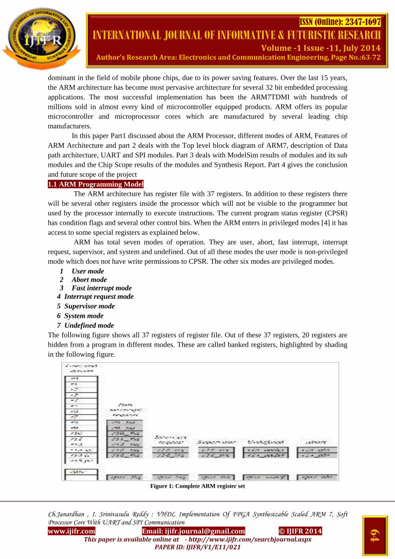
The following figure shows all 37 registers of register file. Out of these 37 registers, 20 registers are
hidden from a program in different modes. These are called banked registers, highlighted by shading
in the following figure.
Figure 1: Complete ARM register set
Page 3
Ch.Janardhan , I. Srinivasulu Reddy : VHDL Implementation Of FPGA Synthesizable Scaled ARM 7, Soft Processor Core With UART and SPI Communication
www.ijifr.com Email: [email protected] © IJIFR 2014 This paper is available online at - http://www.ijifr.com/searchjournal.aspx
PAPER ID: IJIFR/V1/E11/021
ISSN (Online): 2347-1697
INTERNATIONAL JOURNAL OF INFORMATIVE & FUTURISTIC RESEARCH
Volume -1 Issue -11, July 2014 Author’s Research Area: Electronics and Communication Engineering, Page No.:63-72
65
The R0 to R15 are called general purpose registers. These can hold either address or data depending
on the program under execution. The R13, R14 and R15 have some special significance. It is also
possible to use R13 and R14 as general purpose registers depending on the context.
R13 is traditionally used as the stack pointer (SP) and points to the top of the stack in the
current mode of operation.
R14 is called the link register (LR) this stores the return address whenever subroutine is
called.
R15 is the program counter (PC) and contains the address of the next instruction to be fetched
by the processor.
All instructions with respect to R0 to R13 are orthogonal, that is in an instruction if one of these
registers can be used than any other register can be also used. Whereas the registers R14 and R15
have some special usage in few instructions.
1.2 Features of ARM Architecture
The ARM architecture incorporated a number of features from the Berkeley RISC design added with
its own features to improve the performance. Lists of important features of ARM architecture [5] are
described below.
(a) Thumb mode of operation
(b) A load – store architecture
(c) Fixed length 32-bit instructions
(d) 3-Adress instruction format
(e) Large 16 word 32 bit register file
(f) Orthogonal instruction set
(g) mostly single cycle execution
(h) No support for misaligned memory accesses (now supported in ARMv6 cores)
(i) Conditional execution of instructions
(j) Flags are modified only when required
(k) 32-bit barrel shifter which can be used to shift and rotate without performance penalty
(l) Powerful indexed addressing modes
(m) Multi word load store instructions.
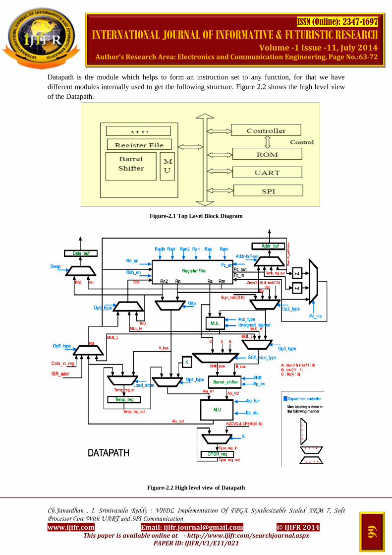
2. Proposed System Description
2.1 Top Level Block Diagram of ARM7
The Top level block diagram of ARM7 Processor with UART and SPI communication shown in the
Figure 2.1.
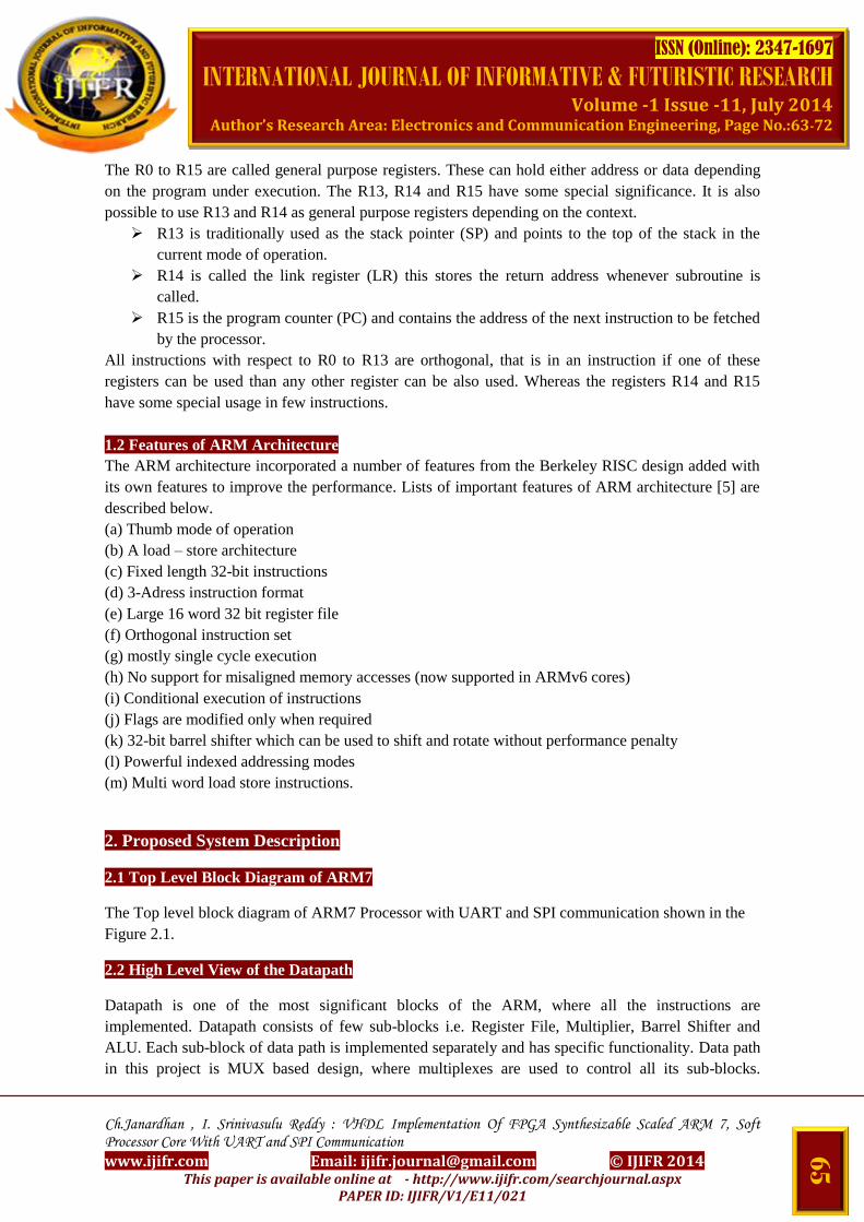
2.2 High Level View of the Datapath
Datapath is one of the most significant blocks of the ARM, where all the instructions are
implemented. Datapath consists of few sub-blocks i.e. Register File, Multiplier, Barrel Shifter and
ALU. Each sub-block of data path is implemented separately and has specific functionality. Data path
in this project is MUX based design, where multiplexes are used to control all its sub-blocks.
Page 4
Ch.Janardhan , I. Srinivasulu Reddy : VHDL Implementation Of FPGA Synthesizable Scaled ARM 7, Soft Processor Core With UART and SPI Communication
www.ijifr.com Email: [email protected] © IJIFR 2014 This paper is available online at - http://www.ijifr.com/searchjournal.aspx
PAPER ID: IJIFR/V1/E11/021
ISSN (Online): 2347-1697
INTERNATIONAL JOURNAL OF INFORMATIVE & FUTURISTIC RESEARCH
Volume -1 Issue -11, July 2014 Author’s Research Area: Electronics and Communication Engineering, Page No.:63-72
66
Datapath is the module which helps to form an instruction set to any function, for that we have
different modules internally used to get the following structure. Figure 2.2 shows the high level view
of the Datapath.
Figure-2.1 Top Level Block Diagram
Figure-2.2 High level view of Datapath
Page 5
Ch.Janardhan , I. Srinivasulu Reddy : VHDL Implementation Of FPGA Synthesizable Scaled ARM 7, Soft Processor Core With UART and SPI Communication
www.ijifr.com Email: [email protected] © IJIFR 2014 This paper is available online at - http://www.ijifr.com/searchjournal.aspx
PAPER ID: IJIFR/V1/E11/021
ISSN (Online): 2347-1697
INTERNATIONAL JOURNAL OF INFORMATIVE & FUTURISTIC RESEARCH
Volume -1 Issue -11, July 2014 Author’s Research Area: Electronics and Communication Engineering, Page No.:63-72
67
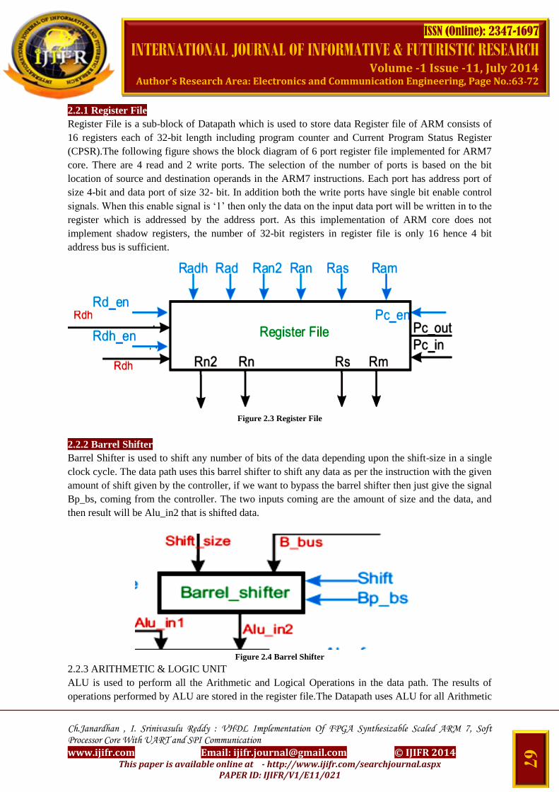
2.2.1 Register File
Register File is a sub-block of Datapath which is used to store data Register file of ARM consists of
16 registers each of 32-bit length including program counter and Current Program Status Register
(CPSR).The following figure shows the block diagram of 6 port register file implemented for ARM7
core. There are 4 read and 2 write ports. The selection of the number of ports is based on the bit
location of source and destination operands in the ARM7 instructions. Each port has address port of
size 4-bit and data port of size 32- bit. In addition both the write ports have single bit enable control
signals. When this enable signal is ‘1’ then only the data on the input data port will be written in to the
register which is addressed by the address port. As this implementation of ARM core does not
implement shadow registers, the number of 32-bit registers in register file is only 16 hence 4 bit
address bus is sufficient.
Figure 2.3 Register File
2.2.2 Barrel Shifter
Barrel Shifter is used to shift any number of bits of the data depending upon the shift-size in a single
clock cycle. The data path uses this barrel shifter to shift any data as per the instruction with the given
amount of shift given by the controller, if we want to bypass the barrel shifter then just give the signal
Bp_bs, coming from the controller. The two inputs coming are the amount of size and the data, and
then result will be Alu_in2 that is shifted data.
Figure 2.4 Barrel Shifter
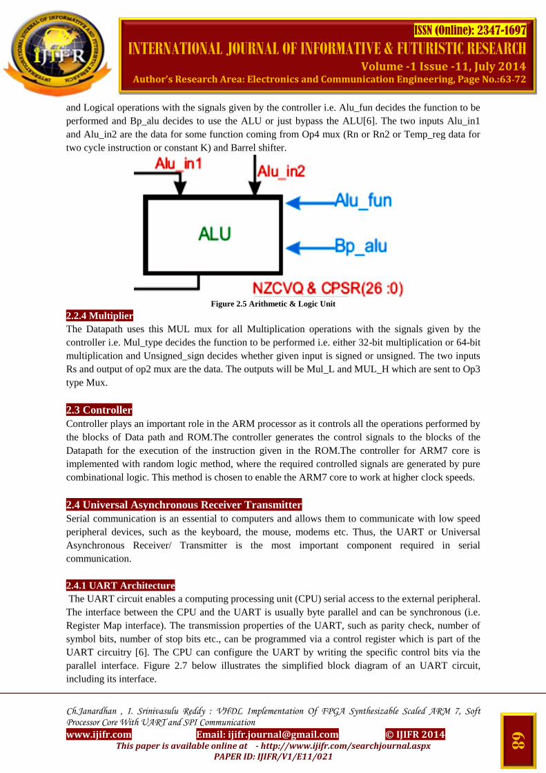
2.2.3 ARITHMETIC & LOGIC UNIT
ALU is used to perform all the Arithmetic and Logical Operations in the data path. The results of
operations performed by ALU are stored in the register file.The Datapath uses ALU for all Arithmetic
Page 6
Ch.Janardhan , I. Srinivasulu Reddy : VHDL Implementation Of FPGA Synthesizable Scaled ARM 7, Soft Processor Core With UART and SPI Communication
www.ijifr.com Email: [email protected] © IJIFR 2014 This paper is available online at - http://www.ijifr.com/searchjournal.aspx
PAPER ID: IJIFR/V1/E11/021
ISSN (Online): 2347-1697
INTERNATIONAL JOURNAL OF INFORMATIVE & FUTURISTIC RESEARCH
Volume -1 Issue -11, July 2014 Author’s Research Area: Electronics and Communication Engineering, Page No.:63-72
68
and Logical operations with the signals given by the controller i.e. Alu_fun decides the function to be
performed and Bp_alu decides to use the ALU or just bypass the ALU[6]. The two inputs Alu_in1
and Alu_in2 are the data for some function coming from Op4 mux (Rn or Rn2 or Temp_reg data for
two cycle instruction or constant K) and Barrel shifter.
Figure 2.5 Arithmetic & Logic Unit
2.2.4 Multiplier
The Datapath uses this MUL mux for all Multiplication operations with the signals given by the
controller i.e. Mul_type decides the function to be performed i.e. either 32-bit multiplication or 64-bit
multiplication and Unsigned_sign decides whether given input is signed or unsigned. The two inputs
Rs and output of op2 mux are the data. The outputs will be Mul_L and MUL_H which are sent to Op3
type Mux.
2.3 Controller
Controller plays an important role in the ARM processor as it controls all the operations performed by
the blocks of Data path and ROM.The controller generates the control signals to the blocks of the
Datapath for the execution of the instruction given in the ROM.The controller for ARM7 core is
implemented with random logic method, where the required controlled signals are generated by pure
combinational logic. This method is chosen to enable the ARM7 core to work at higher clock speeds.
2.4 Universal Asynchronous Receiver Transmitter
Serial communication is an essential to computers and allows them to communicate with low speed
peripheral devices, such as the keyboard, the mouse, modems etc. Thus, the UART or Universal
Asynchronous Receiver/ Transmitter is the most important component required in serial
communication.
2.4.1 UART Architecture
The UART circuit enables a computing processing unit (CPU) serial access to the external peripheral.
The interface between the CPU and the UART is usually byte parallel and can be synchronous (i.e.
Register Map interface). The transmission properties of the UART, such as parity check, number of
symbol bits, number of stop bits etc., can be programmed via a control register which is part of the
UART circuitry [6]. The CPU can configure the UART by writing the specific control bits via the
parallel interface. Figure 2.7 below illustrates the simplified block diagram of an UART circuit,
including its interface.
Page 7
Ch.Janardhan , I. Srinivasulu Reddy : VHDL Implementation Of FPGA Synthesizable Scaled ARM 7, Soft Processor Core With UART and SPI Communication
www.ijifr.com Email: [email protected] © IJIFR 2014 This paper is available online at - http://www.ijifr.com/searchjournal.aspx
PAPER ID: IJIFR/V1/E11/021
ISSN (Online): 2347-1697
INTERNATIONAL JOURNAL OF INFORMATIVE & FUTURISTIC RESEARCH
Volume -1 Issue -11, July 2014 Author’s Research Area: Electronics and Communication Engineering, Page No.:63-72
69
Figure 2.7 Simplified Block Diagram of UART
3. Simulation Results
This chapter deals with ModelSim results of the Top level Block Diagram and its modules. The below
simulation results shows the different instructions performed by the ARM processor. The output of
the results stored on the Registers.
Figure 3.1 Simulation result of the Top level diagram
Page 8
Ch.Janardhan , I. Srinivasulu Reddy : VHDL Implementation Of FPGA Synthesizable Scaled ARM 7, Soft Processor Core With UART and SPI Communication
www.ijifr.com Email: [email protected] © IJIFR 2014 This paper is available online at - http://www.ijifr.com/searchjournal.aspx
PAPER ID: IJIFR/V1/E11/021
ISSN (Online): 2347-1697
INTERNATIONAL JOURNAL OF INFORMATIVE & FUTURISTIC RESEARCH
Volume -1 Issue -11, July 2014 Author’s Research Area: Electronics and Communication Engineering, Page No.:63-72
70
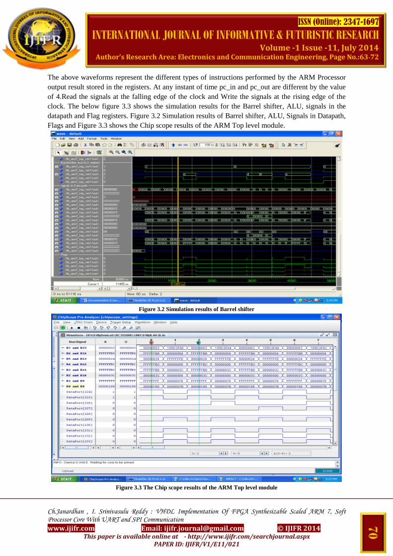
The above waveforms represent the different types of instructions performed by the ARM Processor
output result stored in the registers. At any instant of time pc_in and pc_out are different by the value
of 4.Read the signals at the falling edge of the clock and Write the signals at the rising edge of the
clock. The below figure 3.3 shows the simulation results for the Barrel shifter, ALU, signals in the
datapath and Flag registers. Figure 3.2 Simulation results of Barrel shifter, ALU, Signals in Datapath,
Flags and Figure 3.3 shows the Chip scope results of the ARM Top level module.
Figure 3.2 Simulation results of Barrel shifter
Figure 3.3 The Chip scope results of the ARM Top level module
Page 9
Ch.Janardhan , I. Srinivasulu Reddy : VHDL Implementation Of FPGA Synthesizable Scaled ARM 7, Soft Processor Core With UART and SPI Communication
www.ijifr.com Email: [email protected] © IJIFR 2014 This paper is available online at - http://www.ijifr.com/searchjournal.aspx
PAPER ID: IJIFR/V1/E11/021
ISSN (Online): 2347-1697
INTERNATIONAL JOURNAL OF INFORMATIVE & FUTURISTIC RESEARCH
Volume -1 Issue -11, July 2014 Author’s Research Area: Electronics and Communication Engineering, Page No.:63-72
71
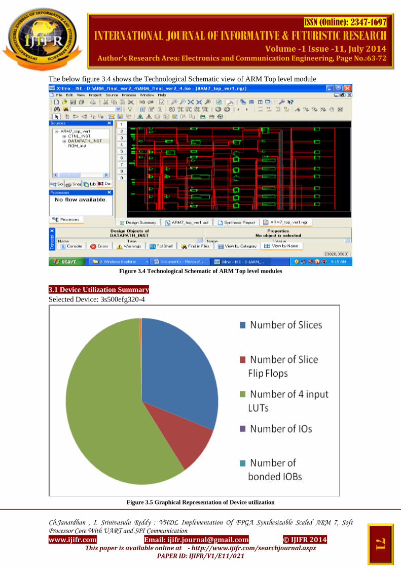
The below figure 3.4 shows the Technological Schematic view of ARM Top level module
Figure 3.4 Technological Schematic of ARM Top level modules
3.1 Device Utilization Summary
Selected Device: 3s500efg320-4
Figure 3.5 Graphical Representation of Device utilization
Page 10
Ch.Janardhan , I. Srinivasulu Reddy : VHDL Implementation Of FPGA Synthesizable Scaled ARM 7, Soft Processor Core With UART and SPI Communication
www.ijifr.com Email: [email protected] © IJIFR 2014 This paper is available online at - http://www.ijifr.com/searchjournal.aspx
PAPER ID: IJIFR/V1/E11/021
ISSN (Online): 2347-1697
INTERNATIONAL JOURNAL OF INFORMATIVE & FUTURISTIC RESEARCH
Volume -1 Issue -11, July 2014 Author’s Research Area: Electronics and Communication Engineering, Page No.:63-72
72
4. Conclusion & Future Scope
4.1 Conclusion ARM soft processor core were implemented in the context of FPGA based multiprocessor based SOC
applications. All the 32-bit instructions were implemented with single cycle datapath and random
logic based instruction decoder. The instructions of Data processing, Arithmetic, Branch instructions,
Logical and compare were implemented. The data path was implemented with multiplexer based
design, which is suitable for FPGA implementation. GNU ARM assembler generated hex codes was
used to validate the design. UART and SPI cores were memory mapped through dedicated addresses.
The design is functionally verified using ModelSim simulator. The design occupies 48% on the
Spartan 3E FPGA family of device xc3s500e-4fg320.
4.2 Future Scope
Alternatively the design can also be implemented on high end FPGA devices like Virtex4 or Virtex5
for better speeds. ARM cores can be used for verification platforms in the industries.
5. References
[1] Virtual ARM Platform for Embedded System Developers, Alex Heunhe Han, Young-Si Hwang, Young-Ho
An, So-Jin Lee, Ki-Seok Chung Dept. of Electronics and Computer & Communications Engineering, Hanyang
University,IEEE 2008
[2] DESIGN OF 32-BIT RISC PROCESSOR AND EFFICIENT VERIFICATION Geun-young Jeong, Dept. of
Electronics Engineering, Pusan National University, Korea.
[3] ARM System Developer’s Guide designed and optimized system software by Andrew N.sloss, Dominic
symes, Chris Wright.
[4] ARM Architecture Reference Manual
[5] A Design Flow For Embedding The ARM Processor In An ASIC Dave Auer & Mark Buer VLSI
Technology, Inc.
[6] ARM Ltd, 1995, ARh47TDMI Data Sheet (ARM DDI 0029E), Advanced RISC Machines Ltd.
[7] http://www.rpi.edu/dept/ecse/mps/SPI.pdfhttp://www.cse.unsw.edu.au/~cs3221/labs/assembler-intro.pdf
Ch. Janardhan working as an Asst. Professor in the Department of ECE at
Priyadarshini College Of Engg & Technology Nellore- 524004, A.P, India. He is
having 5 years of Experience in Teaching. His area of research is Low Power VLSI
and Communication Systems. He is a life member in IACSIT.
I. Srinivasulu Reddy working as an Asst. Professor in the Department of ECE at
Priyadarshini College Of Engg & Technology Nellore- 524004, A.P, India. He is
having 5 years of Experience in Teaching. His area of research is VLSI and
Communication Systems.