Page 1
Microelectronics Reliability 45 (2005) 1079–1093
Introductory Invited Paper
Chip-packaging interaction: a critical concernfor Cu/low k packaging
Guotao Wang a,*, Paul S. Ho a, Steven Groothuis b
a Laboratory for Interconnect and Packaging, University of Texas at Austin, Austin, TX 78712-1063, USAb Micron Technology Texas LLC, 1025 Central Expressway South, Suite 100, Allen, TX 75030, USA
Received 19 November 2004
Available online 21 January 2005
www.elsevier.com/locate/microrel
Abstract
Chip-packaging interaction is becoming a critical reliability issue for Cu/low k chips during package assembly. With
the traditional TEOS interlevel dielectric being replaced by much weaker low k dielectrics, packaging induced interfacial
delamination in low k interconnects has been widely observed, raising serious reliability concerns for Cu/low k chips. In
a flip-chip package, the thermal deformation of the package can be directly coupled into the Cu/low k interconnect
structure inducing large local deformation to drive interfacial crack formation. In this paper, we will first review the
experimental techniques for package thermal deformation measurement and interfacial fracture energy measurement
for low k interfaces. Then 3D finite element analysis (FEA) based on a multilevel sub-modeling approach in combina-
tion with high-resolution Moire interferometry is employed to examine the packaging effect on low k interconnect reli-
ability. Our results indicate that packaging assembly can significantly impact wafer-level reliability causing interfacial
delamination to become a serious reliability concern for Cu/low k structures. Possible solutions and future study are
discussed.
� 2004 Elsevier Ltd. All rights reserved.
1. Introduction
Structural integrity is a major reliability concern for
high-density flip-chip packages due to large deformation
and stresses generated by thermal mismatch between the
silicon die and the substrate. By employing underfills,
thermal stresses at the solder bumps can be effectively re-
duced to improve package reliability [1]. However, the
underfill causes the package to deform, leading to large
peeling stresses at the die–underfill and/or die–solder
0026-2714/$ - see front matter � 2004 Elsevier Ltd. All rights reserv
doi:10.1016/j.microrel.2004.12.008
* Corresponding author. Tel.: +1 512 471 8961; fax: +1 512
471 8969.
E-mail addresses: [email protected] (G. Wang),
[email protected] (P.S. Ho), [email protected]
(S. Groothuis).
interfaces, which significantly impact packaging reliabil-
ity. At this time, the Al/oxide interconnect is being re-
placed by Cu damascene structures with oxide and low
k interlevel dielectrics. Compared with oxide, the low k
dielectric is softer, expands more and adheres weakly
to other materials. For a stand-alone wafer structure be-
fore packaging, under a thermal loading from wafer pro-
cess temperature (400 �C) to room temperature, an
energy release rate of less than 1 J/m2 has been reported
for interfaces in Cu/low k structures [2]. This is about 5·less than fracture energies measured for low k interfaces
by 4-point bend test. While this indicates that interfacial
delamination is not a critical issue for a stand-alone die,
the problem is commonly observed in Cu/low k inter-
connects after assembling the die into a plastic flip-chip
package. This raises an important question concerning
ed.
Page 2
Fig. 1. Flip-chip package attached to substrate with solder
bumps surrounded by underfill.
1080 G. Wang et al. / Microelectronics Reliability 45 (2005) 1079–1093
the effect of packaging driving interfacial delamination
and its impact on the reliability of Cu/low k chips [3–6].
In this article, we first review high-resolution Moire
interferometry, a powerful experimental technique for
measuring thermal deformation in a flip-chip package.
This is followed by a discussion of interfacial fracture
energy measurement for low k interfaces. Then results
from 3D finite element analysis (FEA) to investigate
the chip-package interaction based on a multilevel
sub-modeling approach for low k interconnects are
discussed. Here the modeling results are verified using
thermal deformation measured by high-resolution
Moire interferometry. With a phase-shift technique,
the resolution of Moire interferometry can reach
26 nm per fringe order, which is sufficient to determine
deformation and strain distributions accurately within
a small area, e.g., a solder bump in the package. After
verifying FEA at the packaging level, multilevel sub-
modeling was conducted one level of detail at a time,
extending from the first sub-model level of the package
around the solder bumps with the highest deformation
to the final sub-model level of the Cu/low k interconnect.
Simulation details and problems related to sub-modeling
will be presented and discussed. In the sub-model at the
interconnect level, a crack with fixed length was intro-
duced at relevant interfaces. A modified virtual crack
closure (MVCC) technique was used to calculate the en-
ergy release rate. In our study, with the local stress and
strain distributions obtained by modeling, the compo-
nents of energy release rate corresponding to the three
basic fracture modes 1, 2 and 3 can be separately deter-
mined. This enables us to evaluate the critical energy re-
lease rate at various interfaces with a properly defined
mode mixity. Results for underfilled flip-chip packages
under certain thermal loading conditions are reported
and discussed first. Then packaging effect from the most
critical flip-chip assembly step, die attach (before under-
filling), is discussed. Our results indicate that packaging
assembly can significantly impact wafer-level reliability
causing interfacial delamination to become a serious
reliability concern for Cu/low k structures. Finally, pos-
sible solutions and future study are briefly described.
2. Thermal deformation of electronic packages
As shown in Fig. 1, a flip-chip package is formed by
directly attaching a chip upside-down to a substrate with
solder bumps. The large thermal expansion mismatch
between the silicon die and the substrate introduces sig-
nificant thermal stresses in the package, especially for
the solder bumps along the outer rows. Underfill is com-
monly used to fill the gap between solder bumps in order
to reduce the thermal stresses in the solder bumps hence
improving the solder reliability. However, new interfaces
are introduced with the presence of underfill, such as
solder–underfill, underfill–silicon and underfill–substrate
interfaces. Delamination along these interfaces induced
by thermal stresses generated during thermal cycling is
frequently observed. Thermal deformation in the pack-
age is directly related to its geometry and the materials
used in the package.
Thermal deformation of a flip-chip package can be
determined using an optical technique of Moire interfer-
ometry. This is a whole-field optical interference tech-
nique with high resolution and high sensitivity for
measuring the in-plane displacement and strain distribu-
tions [7]. Recently, this method has been successfully used
to measure the thermal–mechanical deformation in elec-
tronic packages to investigate package reliability [8–10].
A widely used Moire interferometer for electronic pack-
age analysis is the Portable Engineering Moire Interfer-
ometer (PEMI) originated from IBM. In its standard
form, a grating frequency of 1200 lines/mm is used, which
yields a spacing of the interference fringe corresponding
to 417 nmof in-plane displacement. The sensitivity is ade-
quate for measuring the overall thermal deformation of
electronic packages but not sufficient for measuring ther-
mal deformation in high-density electronic packages,
particularly for small features, such as solder bumps.
For such measurements, a high-resolution Moire inter-
ferometry method was developed in our laboratory based
on a phase shifting technique [11]. With this method, a
resolution of 26 nm per fringe was achieved.
The conventional Moire interferometry image is an
interferogram, which carries the in-plane displacement
information. Discrete displacements can be obtained
by counting the fringe order (417 nm per fringe). Fig.
2 shows the optical system of a Moire interferometer.
The phase-shifting technique provides a high-resolu-
tion capability for determining the displacement field
by precisely shifting the phase angle of the two coherent
incident beams to the sample grating. In the interfero-
gram, one fringe spacing corresponds to a phase angle
difference of 2p, corresponding to 417 nm of displace-
ment. Between two interference fringes, the phase angle
varies continuously, so for two points within an interfer-
ence spacing, their relative displacement cannot be
determined explicitly from the interference pattern.
However, such a displacement can be obtained if their
phase angle differrence is determined. Phase-shifting
Moire interferometry extracts the unknown phase angle
as a function of position in the interferogram from four
Page 3
Fig. 2. The optical schematic of a Moire interferometer.
Fig. 3. Phase-shift PEMI with PZT modification mount on the
back plate.
G. Wang et al. / Microelectronics Reliability 45 (2005) 1079–1093 1081
precisely phase-shifted Moire interference patterns. Its
principle can be explained by expressing the intensity
of the four images as [11]
I1ðx; yÞ ¼ I0ðx; yÞ þ I 0ðx; yÞ cos½/ðx; yÞ�;I2ðx; yÞ ¼ I0ðx; yÞ þ I 0ðx; yÞ cos½/ðx; yÞ þ p=2�
¼ I0ðx; yÞ � I 0 sin½/ðx; yÞ�;I3ðx; yÞ ¼ I0ðx; yÞ þ I 0ðx; yÞ cos½/ðx; yÞ þ p�
¼ I0ðx; yÞ � I 0 cos½/ðx; yÞ�;I4ðx; yÞ ¼ I0ðx; yÞ þ I 0ðx; yÞ cos½/ðx; yÞ þ 3p=2�
¼ I0ðx; yÞ þ I 0 sin½/ðx; yÞ�;
ð1Þ
where I0(x,y) and I 0(x,y) are the background and period-
ically varying intensities in the interference pattern and
/(x,y) is the unknown phase angle of the interference
pattern at each pixel location (x,y). Each subsequent
pattern is obtained by consecutively shifting a phase
angle of exactly p/2, or 1/4 of the fringe period. The
unknown phase angle is then determined as
/ ¼ arctanI4 � I2I1 � I3
: ð2Þ
Once the phase angle is obtained, the continuous dis-
placement can be determined; for example, the u field
displacement can be expressed as
u ¼ /4pf
: ð3Þ
The v field displacement has a similar relation as Eq. (3).
The strains can then be evaluated accordingly:
ex ¼ouox
; ey ¼ovoy
; cxy ¼ouoy
þ ovox
: ð4Þ
In operation, phase shifting is achieved by physically
shifting the reference grating. Shifting the reference grat-
ing along the x-direction can phase shift the U field
fringe pattern and shifting the reference grating along
y-direction can phase shift the V field fringe pattern.
To accomplish this, a high-precision PZT piezoelectric
transducer is used to shift the reference grating. An up-
graded IBM PEMI, as shown in Fig. 3 was used for the
Moire experiment. The PEMI system was aligned using
the undeformed 1200 lines/mm grating, which was used
to apply the sample grating. Then the package with de-
formed grating (due to the �80 �C thermal load) on the
cross-section surface was put into the system to capture
the Moire images. Phase-shifting was performed by
shifting the reference grating within the interferometer
using a Melles–Griot PZT piezoelectric transducer.
The reference grating was physically shifted 147, 295
and 441 nm relative to the I1 image in order to generate
the I2, I3 and I4 images. Images were captured using a
Photometrics 1.3 megapixel CCD camera with 12-bit
grayscale sensitivity (4096 grayscales).
3. Low k interfacial strength measurement
The interfacial fracture energy can be determined by
measuring the critical energy release rate. One com-
monly used experimental technique for measuring the
low k interfaces is the 4-point bending test [12], as sche-
matically shown in Fig. 4. Compared with the silicon
wafer, the dielectric layer is very thin hence the sample
structure responses can be assumed to be linearly elastic
and the strain energy stored in the dielectric layer can be
ignored [13]. Accordingly, the critical energy release
rate, GC, can be determined as
GC ¼ 21ð1� m2ÞP 2Cl
2
16EB2h3; ð5Þ
where E and m are the Young�s modulus and Poisson
ratio of silicon, respectively, B is the sample width, h is
the wafer thickness, P is the load, and l is the distance
between inner and outer loading points. PC is the critical
load when the crack propagates along the interface.
Page 4
66 mm
B = 6 mm
crack length, 2a
50 mm
25 mm
Fig. 4. 4-Point bending geometry.
1082 G. Wang et al. / Microelectronics Reliability 45 (2005) 1079–1093
The 4-point bending test can only measure the critical
energy release rate at a fixed phase angle, or mode mix-
ity. Since the critical energy release rate is a function of
mode mixity, an instrument to measure interfacial adhe-
sion energy under mixed mode loading was developed
using the approach originally conceived by Spelt and
co-worker [14,15]. This design utilizes a double cantile-
ver beam (DCB) geometry, as illustrated in Fig. 5. The
instrument allows interfacial fracture measurements for
phase angles ranging from 0� (pure tension) to 90� (pureshear). Additionally, multiple tests can be run on the
same sample. The challenge of this technique resides in
the crack length measurement, which is required for
deducing the fracture energy for the DCB configuration.
aAdhesive layer
F1
F2
(a)
Adjustablet
Adjustable
Adjustablet
S4 S3
S1S2
F
F2
F1
DCB sample
(b)
Fig. 5. Mixed-mode bending test: (a) double cantilever beam
geometry, (b) mixed-mode loading fixture.
The energy release rate per unit crack length can then be
defined as
G ¼ ðF 1aÞ2
2D1þ F 2
F 1
� �2
� 1
81þ F 2
F 1
� �2 !" #
; ð6Þ
where the flexural rigidity per unit width D is given by
D ¼ Eh3
12: ð7Þ
The phase angle, w, varies as function of the ratio F1/F2
w ¼ arctan
ffiffiffi3
p
2
F 1
F 2þ 1
� �F 1
F 2� 1
� �24
35: ð8Þ
4. Chip-packaging interaction
Chip-packaging interaction during assembly is
becoming an increasingly critical reliability issue. Since
traditional ILD material, TEOS, is being replaced by
much weaker low k materials, packaging is suspected
to affect the reliability of Cu/low k interconnects. Pack-
aging induced interfacial delamination along low k
material interfaces has been widely observed. Chip-
packaging interaction has not been a problem for SiO2
interconnects. Unfortunately, this problem has become
a major concern for packaging on Cu/low k structures.
Thermo-mechanical deformations of electronic pack-
ages are directly related to their reliability and have been
investigated using finite element analysis (FEA). For
stand-alone wafer structures, FEA is commonly used
to study thermal stresses in multilevel interconnect struc-
tures. After a die being assembled into a flip-chip pack-
age, the thermal deformation of the whole package can
increase the thermo-mechanical stresses in the intercon-
nect structures at the die surface. To apply FEA to eval-
uate the packaging effect on thermal deformation of the
interconnect structure, there is a basic difficulty due to
the large difference in the dimension of the packaging
and interconnect structures. For this reason, researchers
from Motorola first introduced a multilevel sub-model-
ing technique to evaluate the energy release rate for
interfaces in the interconnect structure after being
assembled into a flip-chip package [16]. This technique
bridged the gap between the packaging and wafer levels.
Energy release rates for various interconnect interfaces
during packaging assembly were calculated using 2D
FEA models. However, a flip-chip package is a compli-
cated 3D structure that cannot be properly represented
using a 2D model. We developed, therefore, a 3D
FEA based on a 4-level sub-modeling technique to
investigate the packaging effect on interconnect reliabil-
ity, particularly focusing on the Cu/low k chips in com-
parison to Al and Cu/oxide chips [17].
Page 5
G. Wang et al. / Microelectronics Reliability 45 (2005) 1079–1093 1083
4.1. Multilevel sub-modeling technique
Level 1:
Starting from the package level, thermal deformation
for a whole flip-chip package was investigated first using
3D FEA. At this package level, a quarter section of the
package was modeled using the symmetry shown in Fig.
6. No interconnect structure detail was considered at
this time because its thickness is too small compared
with the whole package. Simulation results for this
whole package level model were verified with experimen-
tal results obtained from Moire interferometry.
Level 2:
From the simulation results for the package level
modeling, the most critical solder bump was identified.
A sub-model of the package level model (Level 1)
focusing on the critical solder bump region with much
finer meshes was developed as shown in Fig. 7. The
built-in cut boundary technique in ANSYS [18] was
used for sub-modeling. At this sub-model level, a uni-
form ILD layer at the die surface was considered but
still no detailed structure was considered in this sub-
model.
Fig. 6. Package level model.
Fig. 7. Critical solder region model.
Level 3:
Based on the Level 2 modeling results, a large peeling
stress was found at the die–solder interface. At the criti-
cal die–solder interface region with the highest peeling
stress, a sub-model based on a Level 2 model was cre-
ated using the cut boundary technique, as shown in
Fig. 8. This sub-model focused on the die–solder inter-
face region (a small region of Level 2) containing a por-
tion of the die, the ILD layer and a portion of the solder
bump. Still only a uniform ILD layer at the die surface
was considered at this level and no detailed interconnect
structure was included.
Level 4:
This sub-model zoomed in further from the Level 3
model focusing on the die–solder interface region as
shown in Fig. 9. Finally a detailed interconnect structure
was included. Ten lines were found to be sufficient to
approximate the interconnect structure. The sub-model
was set up accordingly and at the center line a crack
with a fixed length was introduced along several inter-
faces of interest. Energy release rate and mode mix-
ity for each crack were determined using a modified
Fig. 8. Die–solder interface level model.
Fig. 9. Detailed wafer level interconnect structure model.
Page 6
1084 G. Wang et al. / Microelectronics Reliability 45 (2005) 1079–1093
virtual crack closure technique as discussed in the next
section.
4.2. Modified virtual crack closure (MVCC) technique
A modified virtual crack closure (MVCC) technique
was used to calculate the energy release rate [19]. Since
the critical energy release rate is a function of mode mix-
ity, the components of the energy release rate corre-
sponding to the three basic fracture modes 1, 2 and 3
(Fig. 10) were separately determined. In our study, with
the local stress and strain distributions obtained by
modeling, the mode mixity for various interfaces can
be properly defined and the critical energy release rate
calculated accordingly.
For the 8-node solid elements shown in Fig. 10, the
three energy release rate components GI, GII and GIII
can be obtained as
GI ¼Xi
F ði1Þz dði2Þz =ð2DAÞ;
GII ¼Xi
F ði1Þx dði2Þx =ð2DAÞ;
GIII ¼Xi
F ði1Þy dði2Þy =ð2DAÞ;
ð9Þ
where F ði1Þx , F ði1Þ
y and F ði1Þz are nodal forces at node i1
along x, y and z direction, respectively. dði2Þx , dði2Þy and
dði2Þz are relative displacements between node i2 and i3along x, y and z direction, respectively. Note that for
simplicity only one element set is shown along crack
front direction (y direction).
Once GI, GII and GIII are determined, the phase an-
gles may be expressed as
)( 1izF
)( 1iz
F
)( 2izδ
)( 1ix
F
)( 1ix
F
)( 2ixδ
)1
)1
∆A ∆A i2
i1
i3
i2 i1i3z
xy
FEA elements and nodes near crack tip Mode1 component
Mode 3 component
i2
i3
(iyF
(iyF
)( 2iyδ
i1i2 i1
Mode 2 componenti3
Fig. 10. Modified virtual crack closure technique.
w ¼ tan�1 GII
GI
� �1=2" #
;
u ¼ tan�1 GIII
GI
� �1=2" #
:
ð10Þ
In the finite element analysis, the ratio of GI, GII or
GIII over the total G(GI + GII + GIII) may change due
to changing the element size around the crack tip, espe-
cially when the element size is very small. In our simula-
tion, the element size is relative large hence the ratio of
GI, GII or GIII over the total G is insensitive to the ele-
ment size. The general interface fracture criterion can
be expressed as
GI
GIC
� �l
þ GII
GIIC
� �m
þ GIII
GIIIC
� �n
¼ 1; ð11Þ
where GIC, GIIC and GIIIC are critical energy release rates
for pure mode 1, 2 and 3, respectively. l, m, n are
constants.
5. Results and discussion
The FEA results for the package level modeling was
compared with Moire experimental results first. Since
the thermal load used in the Moire measurement was
from 102 to 22 �C, we applied the same thermal load
(102–22 �C) in the package level modeling in order to
compare the Moire and FEA results. Detailed Moire re-
sults can be found in Ref. [20]. Fig. 11 shows the z-dis-
placement (package warpage) distribution along the
die center line (line A–A in Fig. 1). The FEA and Moire
results are in good agreement.
After verified with Moire interferometry, FEA was
applied to investigate stand-along wafer structures as
well as the packaging effect. Both Al and Cu intercon-
nect structure with TEOS and SilK as ILD were investi-
gated. A crack with fixed length was introduced at
interested interfaces as shown in Fig. 12. Typical mate-
rial properties used in our simulation are listed in Table
-6
-5
-4
-3
-2
-1
0
0 0.5 1 1.5 2 2.5 3 3.5 4Distance from neutral point (mm)
Dis
plac
emen
t (um
)
Moire resultFEA result
Fig. 11. Comparison of FEA and Moire results.
Page 7
Fig. 12. Cracking along interested interfaces.
1
1.2Al/TEOS StructureCu/TEOS StructureCu/SiLK Structure
G. Wang et al. / Microelectronics Reliability 45 (2005) 1079–1093 1085
1. For stand-alone wafer structures, thermal loading is
set from wafer process temperature (400 �C) to room
temperature (25 �C). When considering the packaging
effect, thermal loading was set from �55 to 125 �C.
Table 1
Wafer level interconnect material properties
Material E (GPa) m a (ppm/�C)
Al 72 0.36 24.0
Cu 122 0.35 17.0
TEOS 66 0.18 0.57
SiLK 2.45 0.35 66.0
MSQ 7.00 0.35 18.0
Table 2
Mode mixity for stand-alone Cu/SiLK structures
Crack 1 Crack 2 Crack 3
GI/G 0.80 0.99 0.98
GII/G 0.20 0.00 0.01
GIII/G 0.00 0.01 0.01
G (J/m2) 0.29 1.16 1.05
5.1. Stand-along wafer structures (thermal load from
400 to 25 �C)
The energy release rates for interfacial fracture along
the six interfaces were first calculated for the stand-alone
chip subjected to a thermal load of 400–25 �C, typicalfor wafer processing. The material properties used are
tabulated in Table 1. As illustrated in Fig. 13, the energy
release rates for all the interfaces in Al/TEOS and Cu/
TEOS structures are generally small, less than 1 J/m2.
The Cu/SiLK structure has a higher energy release rate
for Crack 2 along the SiLK/barrier sidewall and Crack
3 along the barrier/Cu interfaces, both exceeding 1 J/
m2. The mode mixities for interface fracture in Cu/SiLK
structure are shown in Table 2, indicating that the frac-
ture mode for these two cracks is almost pure mode 1.
Compared to the critical energy release rates for low k
interfaces obtained from experiments (larger than 4–
5 J/m2), these values are considerably lower. Hence, crit-
ical crack formation in Cu/low k interconnect structures
during wafer processing is not expected to be a serious
problem although the result does not rule out the possi-
bility of delamination due to sub-critical crack growth.
5.2. Impact of packaging (underfilled package with
thermal load from �55 to 125 �C)
The packaging effect was evaluated using the 4-step
multilevel sub-modeling to calculate the energy release
rate. We assumed a stress-free state at �55 �C for the
whole package and the crack driving force was obtained
at 125 �C to simulate a test condition of �55 to 125 �C.
Crack 4 Crack 5 Crack 6
0.07 0.92 0.99
0.84 0.06 0.01
0.09 0.02 0.00
0.17 0.30 0.28
0
0.2
0.4
0.6
0.8
crack 1 crack 2 crack 3 crack 4 crack 5 crack 6
ERR
(J/m
^2)
Fig. 13. Energy release rates for stand-alone wafer structures
(from 400 to 25 �C).
Page 8
1086 G. Wang et al. / Microelectronics Reliability 45 (2005) 1079–1093
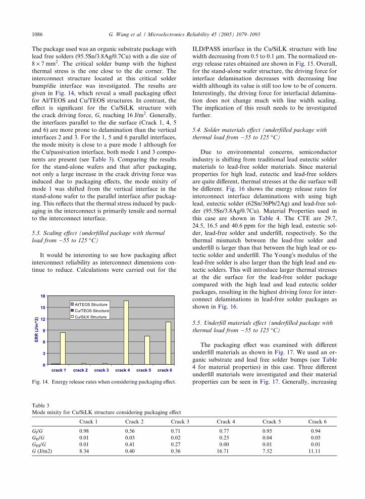
The package used was an organic substrate package with
lead free solders (95.5Sn/3.8Ag/0.7Cu) with a die size of
8 · 7 mm2. The critical solder bump with the highest
thermal stress is the one close to the die corner. The
interconnect structure located at this critical solder
bump/die interface was investigated. The results are
given in Fig. 14, which reveal a small packaging effect
for Al/TEOS and Cu/TEOS structures. In contrast, the
effect is significant for the Cu/SiLK structure with
the crack driving force, G, reaching 16 J/m2. Generally,
the interfaces parallel to the die surface (Crack 1, 4, 5
and 6) are more prone to delamination than the vertical
interfaces 2 and 3. For the 1, 5 and 6 parallel interfaces,
the mode mixity is close to a pure mode 1 although for
the Cu/passivation interface, both mode 1 and 3 compo-
nents are present (see Table 3). Comparing the results
for the stand-alone wafers and that after packaging,
not only a large increase in the crack driving force was
induced due to packaging effects, the mode mixity of
mode 1 was shifted from the vertical interface in the
stand-alone wafer to the parallel interface after packag-
ing. This reflects that the thermal stress induced by pack-
aging in the interconnect is primarily tensile and normal
to the interconnect interface.
5.3. Scaling effect (underfilled package with thermal
load from �55 to 125 �C)
It would be interesting to see how packaging affect
interconnect reliability as interconnect dimensions con-
tinue to reduce. Calculations were carried out for the
0
3
6
9
12
15
18
crack 1 crack 2 crack 3 crack 4 crack 5 crack 6
ERR
(J/m
^2)
Al/TEOS StructureCu/TEOS StructureCu/SiLK Structure
Fig. 14. Energy release rates when considering packaging effect.
Table 3
Mode mixity for Cu/SiLK structure considering packaging effect
Crack 1 Crack 2 Crack 3
GI/G 0.98 0.56 0.71
GII/G 0.01 0.03 0.02
GIII/G 0.01 0.41 0.27
G (J/m2) 8.34 0.40 0.36
ILD/PASS interface in the Cu/SiLK structure with line
width decreasing from 0.5 to 0.1 lm. The normalized en-
ergy release rates obtained are shown in Fig. 15. Overall,
for the stand-alone wafer structure, the driving force for
interface delamination decreases with decreasing line
width although its value is still too low to be of concern.
Interestingly, the driving force for interfacial delamina-
tion does not change much with line width scaling.
The implication of this result needs to be investigated
further.
5.4. Solder materials effect (underfilled package with
thermal load from �55 to 125 �C)
Due to environmental concerns, semiconductor
industry is shifting from traditional lead eutectic solder
materials to lead-free solder materials. Since material
properties for high lead, eutectic and lead-free solders
are quite different, thermal stresses at the die surface will
be different. Fig. 16 shows the energy release rates for
interconnect interface delaminations with using high
lead, eutectic solder (62Sn/36Pb/2Ag) and lead-free sol-
der (95.5Sn/3.8Ag/0.7Cu). Material Properties used in
this case are shown in Table 4. The CTE are 29.7,
24.5, 16.5 and 40.6 ppm for the high lead, eutectic sol-
der, lead-free solder and underfill, respectively. So the
thermal mismatch between the lead-free solder and
underfill is larger than that between the high lead or eu-
tectic solder and underfill. The Young�s modulus of the
lead-free solder is also larger than the high lead and eu-
tectic solders. This will introduce larger thermal stresses
at the die surface for the lead-free solder package
compared with the high lead and lead eutectic solder
packages, resulting in the highest driving force for inter-
connect delaminations in lead-free solder packages as
shown in Fig. 16.
5.5. Underfill materials effect (underfilled package with
thermal load from �55 to 125 �C)
The packaging effect was examined with different
underfill materials as shown in Fig. 17. We used an or-
ganic substrate and lead free solder bumps (see Table
4 for material properties) in this case. Three different
underfill materials were investigated and their material
properties can be seen in Fig. 17. Generally, increasing
Crack 4 Crack 5 Crack 6
0.77 0.95 0.94
0.23 0.04 0.05
0.00 0.01 0.01
16.71 7.52 11.11
Page 9
0
0.2
0.4
0.6
0.8
1
1.2
0.1 0.2 0.3 0.4 0.5Line width (um)
Nor
mal
ized
ER
R
wafer level only (400--25°C)Packaging effect (-55--125°C)
(a)
0
0.2
0.4
0.6
0.8
1
1.2
0.1 0.2 0.3 0.4 0.5Line width (um)
Nor
mal
ized
ER
R
wafer level only (400--25°C)Packaging effect (-55--125°C)
(b)
0
0.2
0.4
0.6
0.8
1
1.2
0.1 0.2 0.3 0.4 0.5Line width (um)
Nor
mal
ized
ER
R
wafer level only (400--25°C)Packaging effect (-55--125°C)
(c)
Fig. 15. Scaling effect: (a) Al/TEOS structure, TEOS/PASS
interface; (b) Cu/TEOS structure, TEOS/PASS interface;
(c) Cu/SiLK structure, SiLK/PASS interface.
0
3
6
9
12
15
18
crack 1 crack 2 crack 3 crack 4 crack 5 crack 6
ERR
(J/m
^2)
High lead solder packageEutectic solder packageLead-free solder package
Fig. 16. Energy release rates for Cu/SiLK structure in high
lead, eutectic solder and lead-free solder packages.
Table 4
Packaging material properties
Solder material E (GPa) m a (ppm/�C)
Eutectic 75.84–0.152T 0.35 24.5
High lead 39.22–0.063T 0.35 29.7
Lead-free 88.53–0.142T 0.40 16.5
Underfill 6.23 0.40 40.6
Ceramic substrate 300 0.3 5.0
Organic substrate Anisotropic
elastic
16 (in plane),
84 (out of plane)
0
3
6
9
12
15
18
crack 1 crack 2 crack 3 crack 4 crack 5 crack 6
ERR
(J/m
^2)
Underfill: E=8.4GPa, CTE=28.0ppmUnderfill: E=7.1GPa, CTE=34.0ppmUnderfill: E=6.2GPa, CTE=40.6ppm
Fig. 17. Energy release rates for Cu/SiLK structure in lead-free
solder packages with different underfill materials.
G. Wang et al. / Microelectronics Reliability 45 (2005) 1079–1093 1087
the CTE of underfill increases the thermal mismatch be-
tween the underfill and solder bumps. Meanwhile,
underfill with a higher CTE has a lower Young�s modu-
lus that will put a weaker protection for solder bumps.
As a result, increasing the CTE of underfill increases
the crack driving force for low k interfacial delamination
under the critical solder bump (see Fig. 17).
5.6. Impact of die attach process on flip-chip package
reliability
Fig. 18 briefly shows the major steps of flip-chip
packaging process. The most critical process step in
flip-chip packaging is the die attach (also called as chip
Die preparation Die
Die attach (Solder reflow)
Substrate
High stress at die/solder interfacewhen cooling down to room temp.
Underfilling 125° to 180°C
Thermal cycling -55 °C-125 °C
Fig. 18. Flip-chip packaging process.
Page 10
1088 G. Wang et al. / Microelectronics Reliability 45 (2005) 1079–1093
joint) step before underfilling the package. The die and
substrate are attached together by solder reflow at a
temperature higher than the solder melting temperature.
After solder reflow, the package structure is cooled
down to room temperature. Without underfill serves as
a stress buffer, thermal mismatch between the die and
substrate can generate large thermal stress at the sol-
der/die interface near the die corner to cause low k inter-
facial delaminations under the UBM layer. In this
section we will examine the effect of the die attach step
on reliability for Cu/low k structures.
The effect of the die attach step on reliability for
low-k structure was first investigated for Cu/SiLK
structures due to different solder materials. These in-
cluded the high lead, eutectic (62Sn/36Pb/2Ag) and
lead-free (95.5Sn/3.8Ag/0.7Cu) solders, which have dif-
ferent reflow temperatures and thermal loads: 160–
25 �C for eutectic solder, 250–25 �C for lead free solder
and 300–25 �C for high lead solder. See Table 4 for
material properties. The substrate in the package was
organic and with a die size of 8 · 7 mm2. Here we as-
sumed that the high lead solder can be assembled onto
an organic substrate in order to compare these three
solders with the same substrate, This assumption may
not be valid for real application since the reflow tem-
peratures can exceed that for organic substrates to han-
dle. Results are summarized in Fig. 19(a) for Cu/SiLK
chips assembled on an organic substrate. The eutectic
0
6
12
18
24
30
36
crack 1 crack 2 crack 3 crack 4 crack 5 crack 6
ERR(
J/m
^2)
High lead solder packageEutectic solder packageLead-free solder package
0
3
6
9
12
crack 1 crack 2 crack 3 crack 4 crack 5 crack 6
ERR
(J/m
^2)
Eutectic solder package
Lead-free solder package
(a)
(b)
Fig. 19. Energy release rates for (a) Cu/SiLK and (b) Cu/MSQ
structures in die attach process: solder materials effect.
solder package has the lowest crack driving force for
interfacial delamination due to its lowest reflow temper-
ature. In contrast, the lead free solder package is most
critical due to the relative high reflow temperature and
the high Young�s modulus of the lead free solder mate-
rial. For the high lead solder, although it has the high-
est reflow temperature, but with the lowest Young�smodulus, the crack driving force is lower than that
for the lead free solder package. The study on the im-
pact of the die attach process was extended to the
Cu/MSQ structure. The results for eutectic and lead-
free solders are shown in Fig. 19(b). The energy release
rate for the Cu/MSQ structure is generally about a fac-
tor of 3 lower than that of the Cu/SiLK structure. In a
later discussion, we attribute this result to the 3· higher
Young�s modulus of the MSQ dielectrics, indicating
that the mechanical property of the low k is an impor-
tant factor to consider for the packaging effect.
Comparing Figs. 14 and 19(a), it is clear that the
crack driving force for delaminations in Cu/SiLK
structures during the die attach process is generally
much larger than that in an underfilled package with
a thermal loading from �55 to 125 �C. This indicates
that the die attach process with a larger thermal load
is a more critical step than thermal cycling in driv-
ing critical interfacial delaminations in Cu/low k
structures.
0
2
4
6
8
crack 1 crack 2 crack 3 crack 4 crack 5 crack 6
ERR
(J/m
^2)
Plastic substrate
Ceramic substrate
0
1
2
3
4
crack 1 crack 2 crack 3 crack 4 crack 5 crack 6
ERR
(J/m
^2)
Plastic substrate
Ceramic substrate
(a)
(b)
Fig. 20. Energy release rates for (a) Cu/SiLK and (b) Cu/MSQ
structures in the die attach process: substrate effect.
Page 11
G. Wang et al. / Microelectronics Reliability 45 (2005) 1079–1093 1089
The effect of the die attach process on interconnect
reliability was also investigated for two flip-chip pack-
ages, one with an organic substrate and the other a
ceramic substrate. Eutectic solders were used in these
packages with a die size of 8 · 7 mm2. See Table 4
for material properties. The results obtained for Cu/
SiLK and Cu/MSQ structures are shown in Fig. 20.
Since the thermal mismatch between the die and the
ceramic substrate is very small, a small thermal stress
is induced in the ceramic substrate package leading to
a small crack driving forces for interfacial delamina-
tion. In this way, the die attach effect for packages with
a ceramic substrate was found to be much better than
the organic substrate for both Cu/SiLK and Cu/MSQ
structures.
Finally, we investigated the packaging effect for the
die attach process as a function of die size using organic
substrate packages with eutectic solder bumps. The re-
sults are shown in Fig. 21 for die sizes of 8 · 7 and
14.4 · 13.4 mm2. The crack driving force in general in-
creases with an increase in die size, which is also to be
expected. However, the die size effect is not as significant
as we expected. The crack driving force only increases
about 15% with the die size almost doubling. In this
study, we only looked at the critical solder region (close
to the die corner). For a small die package, the stress can
still be very high when close to the die corner due to the
stress concentration effect at the die corner.
10
8x7mm Die
14.4x13.4mm Die8
ERR
(J/m
^2) 6
4
2
0crack 1 crack 2 crack 3 crack 4 crack 5 crack 6
4
8x7mm Die
14.4x13.4mm Die
2
3
ERR
(J/m
^2)
1
0crack 1 crack 2 crack 3 crack4 crack 5 crack 6
(a)
(b)
Fig. 21. Energy release rates for (a) Cu/SiLK and (b) Cu/MSQ
structures in die attach process: die size effect.
Fig. 22. Normal stress (rz) in (a) Cu/SiLK and (b) Cu/MSQ
structures induced from the die attach process.
The above results of packaging effect for SiLK and
MSQ low k dielectrics show that the MSQ material in
general has a smaller crack driving force. We examined
this question and found that no matter what low k mate-
rial is used in the interconnect structure at the chip sur-
face, the thermal stress at the die/solder bump interface
induced from the die attach process is almost the same.
This is because the dimension of the low k structure is
very small comparing to the dimension of the packaging
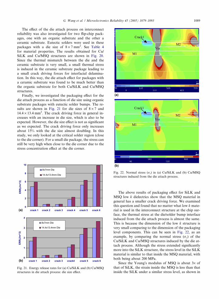
level components. This can be seen in Fig. 22, as an
example, by comparing the normal stress (rz) of the
Cu/SiLK and Cu/MSQ structures induced by the die at-
tach process. Although the stress extended significantly
more into the SiLK structure, the stress level in the SiLK
material is similar to that inside the MSQ material, with
both being about 200 MPa.
Since the Young�s modulus of MSQ is about 3· of
that of SiLK, the strain inside the MSQ is less than that
inside the SiLK under a similar stress level, as shown in
Page 12
Fig. 23. Normal strain (ez) in (a) Cu/SiLK and (b) Cu/MSQ
structures induced from the die attach process.
-400
-200
0
200
400
600
800
0 100 200 300 400 500
Temperature (°C)
Cu
line
stre
ss (M
Pa) Sx
SySz
(a)
800
1090 G. Wang et al. / Microelectronics Reliability 45 (2005) 1079–1093
Fig. 23. So the strain energy induced in the MSQ mate-
rial during packaging assembly will be smaller than that
in SiLK. This leads to a smaller energy release rate, or a
crack driving force for interfacial delamination in the
Cu/MSQ structure.
-400
-200
0
200
400
600
0 100 200 300 400 500
Cu
line
stre
ss (M
Pa)
SxSySz
Simulation
(b) Temperature (°C)
Fig. 24. Residual stresses in Cu lines obtained from FEA and
X-ray measurement for Cu/SiLK structure: (a) X-ray result;
(b) simulation result.
6. Future study
6.1. Effect of residual stress induced from wafer
processing
The above research results show that packaging can
significantly impact the reliability for wafer level Cu/
low k interconnect structures. However, packaging effect
is not the only driving force for Cu/low k interfacial
delamination. Before packaging, residual stress can be
generated during wafer processing. After packaging,
packaging induced stress will superimpose onto the
residual stress generated from wafer processing causing
Cu/low k interfacial delamination.
Wafer processing is a multistep thermal process. The
lowest process temperature can be as low as �20 �C and
the highest as high as 450 �C during wafer processing. In
general, materials incorporated in the wafer structure
can have very different properties. For example, TEOS
has a coefficient of thermal expansion (CTE) of only
0.57 ppm, while Cu—a metal line material—has a CTE
of 17 ppm. Large thermal mismatches between wafer
structure materials can be induced during wafer process-
ing. Hence, severe residual thermal stress can be gener-
ated in the wafer structure during and after wafer
processing. Further more, Cu films can undergo signifi-
cant grain growth during post-ECD annealing, leading
to a stress state change in Cu films. Residual stress, gen-
erated by wafer processing, can have a significant impact
on the reliability of wafer level interconnect structures,
such as stress-induced voiding in Cu lines and vias, elec-
tromigration related problems in Cu lines and interfacial
delaminations and cracking in wafer level interconnect
structures.
Residual stress induced by wafer processing has been
investigated [21,22]. Fig. 24 shows the residual
stresses of Cu lines in a single damascene Cu/SiLK struc-
ture from room temperature to 400 �C after wafer
Page 13
G. Wang et al. / Microelectronics Reliability 45 (2005) 1079–1093 1091
processing. The stress along the Cu line direction (Sx) is
about 500 MPa at room temperature, indicating a high
residual stress level in the Cu/low k structure. In the fu-
ture study, residual stress in Cu/low k structures should
be taken into account together with packaging effect in
order to understand packaging reliability for Cu/low k
structures.
6.2. Package design and assembly process optimization
In order to decrease the packaging impact on reliabil-
ity for Cu/low k structures, attention should be focused
on package optimization including materials selection
and structural design as well as assembly processes.
For example, one may choose ceramic substrates instead
of organic substrates although this may raise a cost
issue.
For flip-chip packaging, selecting a proper underfill
material is an easy and may be an effective way to
decrease the stress in Cu/low k structures induced by
packaging effect. From the previous results reported
in this article, one can see that packaging induced
cracking force is small for Cu/MSQ structures hence
critical MSQ interface delaminations may not be a
problem even for die attach process. However, sub-crit-
ical crack growth is still a concern for packaged MSQ
structures during thermal cycling. Since delamination
typically starts at the die/underfill interface from the
die corner in a flip-chip package, low Tg underfills have
been applied in order to decrease the thermal stress
level at the die corner. However, this can increase the
stress level in solder bumps making Cu/low k interfacial
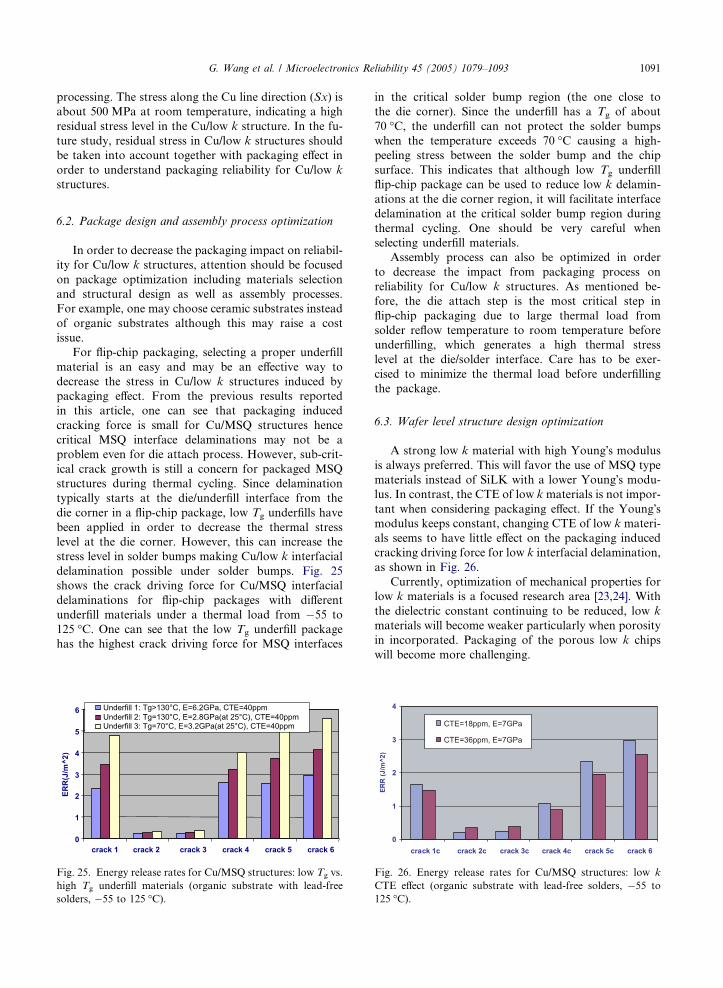
delamination possible under solder bumps. Fig. 25
shows the crack driving force for Cu/MSQ interfacial
delaminations for flip-chip packages with different
underfill materials under a thermal load from �55 to
125 �C. One can see that the low Tg underfill package
has the highest crack driving force for MSQ interfaces
0
1
2
3
4
ERR
(J/m
^2)
5
6
crack 1 crack 2 crack 3 crack 4 crack 5 crack 6
Underfill 1: Tg>130°C, E=6.2GPa, CTE=40ppmUnderfill 2: Tg=130°C, E=2.8GPa(at 25°C), CTE=40ppmUnderfill 3: Tg=70°C, E=3.2GPa(at 25°C), CTE=40ppm
Fig. 25. Energy release rates for Cu/MSQ structures: low Tg vs.
high Tg underfill materials (organic substrate with lead-free
solders, �55 to 125 �C).
in the critical solder bump region (the one close to
the die corner). Since the underfill has a Tg of about
70 �C, the underfill can not protect the solder bumps
when the temperature exceeds 70 �C causing a high-
peeling stress between the solder bump and the chip
surface. This indicates that although low Tg underfill
flip-chip package can be used to reduce low k delamin-
ations at the die corner region, it will facilitate interface
delamination at the critical solder bump region during
thermal cycling. One should be very careful when
selecting underfill materials.
Assembly process can also be optimized in order
to decrease the impact from packaging process on
reliability for Cu/low k structures. As mentioned be-
fore, the die attach step is the most critical step in
flip-chip packaging due to large thermal load from
solder reflow temperature to room temperature before
underfilling, which generates a high thermal stress
level at the die/solder interface. Care has to be exer-
cised to minimize the thermal load before underfilling
the package.
6.3. Wafer level structure design optimization
A strong low k material with high Young�s modulus
is always preferred. This will favor the use of MSQ type
materials instead of SiLK with a lower Young�s modu-
lus. In contrast, the CTE of low kmaterials is not impor-
tant when considering packaging effect. If the Young�smodulus keeps constant, changing CTE of low k materi-
als seems to have little effect on the packaging induced
cracking driving force for low k interfacial delamination,
as shown in Fig. 26.
Currently, optimization of mechanical properties for
low k materials is a focused research area [23,24]. With
the dielectric constant continuing to be reduced, low k
materials will become weaker particularly when porosity
in incorporated. Packaging of the porous low k chips
will become more challenging.
0
1
2
3
4
crack 1c crack 2c crack 3c crack 4c crack 5c crack 6
ERR
(J/m
^2)
CTE=18ppm, E=7GPa
CTE=36ppm, E=7GPa
Fig. 26. Energy release rates for Cu/MSQ structures: low k
CTE effect (organic substrate with lead-free solders, �55 to
125 �C).
Page 14
1092 G. Wang et al. / Microelectronics Reliability 45 (2005) 1079–1093
Metal density can also play an important role
when considering packaging effect. If metal density
is very low at some region, it is easy for low k inter-
faces to delaminate under packaging induced stress.
Mechanical vias may be needed to support the low
k materials. A stronger and thicker passivation layer
can also make the stress distribution in the Cu/low
k structure more uniform hence it may be able to de-
crease the maximum stress level in the structure. The
wafer level structure design can be optimized to
decrease the packaging impact on low k interfacial
delamination.
7. Conclusions
In this paper, we summarize experimental and mod-
eling results from studies performed in our laboratory
to investigate the chip-package interaction and its im-
pact on low k interconnect reliability. We first review
the application of high-resolution Moire interferometry
to measure thermal deformation in a flip-chip package.
Then results from 3D finite element analysis (FEA)
based on a multilevel sub-modeling approach in combi-
nation with high-resolution Moire interferometry to
investigate the chip-package interaction for low k inter-
connects are discussed. Packaging induced crack
driving forces for relevant interfaces in Cu/low k struc-
tures are deduced and compared with corresponding
interfaces in Cu/TEOS and Al/TEOS structures to as-
sess the effect of ILD on packaging reliability. For a
stand-alone chip, the energy release rate driving interfa-
cial delamination during wafer processing is found to
be lower than the critical energy release rate for interfa-
cial delamination obtained from 4-point bend test.
After the die is assembled into a flip-chip package, ther-
mal deformation at the package level can be directly
coupled into the interconnect structure. This can signif-
icantly increase the driving force for interfacial delami-
nation and seriously impact the chip reliability,
especially for Cu/low k structures. Interfaces in the
interconnect structures parallel to the die surface are
more prone to the packaging effect. The packaging ef-
fect was investigated as a function of line width and
the energy release rate does not seem to change with
decreasing line width. During die attach process, a
lead-free solder package can impact the interconnect
reliability more than the eutectic and high lead solders.
Using ceramic substrate is better than using plastic sub-
strate. Increasing die size will increase the crack driving
force for low k interfacial delamination. The Cu/MSQ
structure is better than the Cu/SiLK structure concern-
ing the impact from the die attach process on flip-chip
package reliability.
References
[1] Tsukada Y, Mashimoto Y. Proc surface mount intl, San
Jose, August–September 1992. p. 294–9.
[2] Du Y. PhD thesis. The University of Texas at Austin; 2001.
[3] Mercado L, Goldberg C, Kuo S, Lee T, Pozder S. Analysis
of flip-chip packaging challenges on copper low-k inter-
connects. In: Proc 53th electronic components and tech-
nology conference, 2003. p. 1784–90.
[4] Wang G, Merrill C, Zhao J-H, Groothuis S, Ho PS.
Packaging effects on reliability of Cu/low k interconnects.
IEEE Trans Device Mater Reliab 2003;3(4):119–28.
[5] Edelstein D et al. Comprehensive reliability evaluation of a
90 nm CMOS technology with Cu/PECVD low-k BEOL.
In: Proc 42th IRPS, 2004.
[6] Landers W, et al. Chip-to-package interaction for a 90 nm
Cu/PECVD low-k technology. In: Proc IITC 2004. p. 108–
10.
[7] Post D, Han DB, Ifju P. High Sensitivity Moire: Exper-
imental Analysis for mechanics and Materials. New
York: Springer-Verlag; 1994.
[8] Wang G, Ho P, Hayden T, Pyun E, Gundel D. Solder joint
stress in a cavity-up flex-based BGA. Chip Scale Review,
Technical Forum; April 2001.
[9] Dai X, Ho PS. Thermo-mechanical deformation of under-
filled flip-chip packaging. In: 21st IEEE/CPM Interna-
tional Electronics Manufacturing Technology Symposium.
p. 326–33.
[10] Guo Y, Lim CK, Chen WT, Woychik CG. Solder
ball connect (SBC) assemblies under thermal loading:
I. Deformation measurement via Moire interferome-
try, and its interpretation. IBM J Res Develop 1993;
37:635–48.
[11] Miller Mikel R, Mohammed I, Dai X, Jiang N, Ho PS.
Analysis of flip-chip packages using high resolution Moire
interferometry. In: Proc 49th electronic components and
technology conference, 1999. p. 979–86.
[12] Charalambides PG, Lund J, Evans AG, McMeeking RM.
J Appl Mech 1989;56:77–82.
[13] Suo Z, Hutchinson JW. Sandwich test specimens for
measuring interface crack toughness. Mater Sci Eng A
1989;107:135–43.
[14] Fernlund G, Spelt JK. Comp Sci Tech 1994;50:441–9.
[15] Wylde JW, Spelt JK. Int J Adhesion Adhes 1998;18:
237–46.
[16] Mercado L, Goldberg C, Kuo S. A simulation method for
predicting packaging mechanical reliability with low k
dielectrics. In: Proc int interconnect tech conf, 2002.
[17] Wang G, Groothuis S, Ho PS. Effect of packaging on
interfacial cracking in Cu/low k damascene structures. In:
ECTC, 2003.
[18] ANSYS manual.
[19] Bucholz FG, Sistla R, Krishnamurthy T. 2D- and 3D-
applications of the improved and generalized Modified
Crack Closure Integral Method. In: Atluri SN, Yagawa G,
editors. Computational Mechanics�88. New York: Sprin-
ger-Verlag; 1988.
[20] Wang G, Zhao J-H, Ding M, Ho P. Thermal deformation
analysis on flip-chip packages using high resolution Moire
interferometry. In: Itherm 2002.
Page 15
G. Wang et al. / Microelectronics Reliability 45 (2005) 1079–1093 1093
[21] Wang G. PhD thesis, The University of Texas at Austin;
2004.
[22] Gan D et al. Effects of dielectric material and linewidth on
thermal stresses of Cu line structures. In: Proc int
interconnect tech conf, 2002.
[23] Maex K et al. Low dielectric constant materials
for microelectronics. J Appl Phys 2003;93:8793–
841.
[24] Ho PS et al., editors. Low Dielectric Constant Materials
for IC Applications. Berlin: Springer; 2003.