21
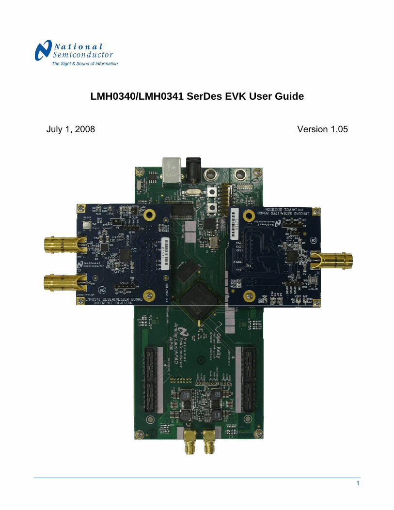
1 LMH0340/LMH0341 SerDes EVK User Guide July 1, 2008 Version 1.05
1
LMH0340/LMH0341 SerDes EVK User Guide
July 1, 2008 Version 1.05
2
1.... Overview 3
2.... Evaluation Kit (SD3GXLEVK) Contents 3
3.... Hardware Setup 4 3.1 ALP100 BOARD (MAIN BOARD) DESCRIPTION 5 3.2 SD340EVK BOARD DESCRIPTION 5 3.3 SD341EVK BOARD DESCRIPTION 6 3.4 LMH0340/LMH0341 SERDES EVK DEFAULT CONNECTIONS (LOOP-BACK) 6
4.... Software Setup 7 4.1 SYSTEM REQUIREMENTS 7 4.2 INSTALLATION 7 4.3 STARTUP 8
5.... Evaluating Hardware 9 5.1 TEST SETUPS 9
5.1.1 Loop-back Tests 9 5.1.2 External Tests 10 5.1.3 Pass-through Tests 10
5.2 EVALUATING SD/HD/3G SDI 11 5.2.1 Video Pattern Generation: Transmit Data Path 12 5.2.2 Embeded Audio Generation: Transmit Data Path 13 5.2.3 Video Format Detect, Audio Detect, CRC and EDH Check: Receive Data Path 13 5.2.4 Deserializer Re-clocked Loop-through: Receive Data Path 14 5.2.5 Pass-through: Receive, Transmit Data Path 14
5.3 EVALUATING USING BIT ERROR RATE TESTER ENGINE 15 5.3.1 Data Pattern Generation: Transmit Data Path 16 5.3.2 Error Injection: Transmit Data Path 17 5.3.3 Data Pattern Verification: Receive Data Path 17 5.3.4 Deserializer Re-clocked Loop-through: Receive Data Path 17 5.3.5 External Clock I/O 17
6.... Documentation 18 6.1 SCHEMATICS, BOMS, AND DATA SHEETS 18 6.2 REFERENCE FPGA IP 18
7.... Part Numbers 18
8.... Trouble Shooting 19
3
1 Overview The LMH0340/LMH0341 SerDes Evaluation Kit (EVK) enables rapid evaluation of the LMH0340/0341 serializer and deserializer in Serial Digital Interface (SDI) applications. All parts in this family can be supported by this EVK. Tables 1 and 2 list the parts in the family and their features.
Table 1) Serializers Device SMPTE 424M
Support SMPTE 292MSupport
SMPTE 259MSupport
DVB-ASI Support
SMPTE Compliant Cable Driver
LMH0340 ☺ ☺ ☺ ☺ ☺ LMH0040 ☺ ☺ ☺ ☺ LMH0070 ☺ ☺ ☺ LMH0050 ☺ ☺ ☺
Table 2) Deserializers
Device SMPTE 424M Support
SMPTE 292MSupport
SMPTE 259MSupport
DVB-ASI Support
Active Loop-through
LMH0341 ☺ ☺ ☺ ☺ ☺ LMH0041 ☺ ☺ ☺ ☺ LMH0071 ☺ ☺ ☺ LMH0051 ☺ ☺ ☺
Examples of firmware are provided for the Standard Definition SMPTE 259M (SD-SDI) interface, the High Definition SMPTE 292M (HD-SDI) interface, the 3G SMPTE 424M (3G-SDI) interface, and general purpose data generator with Bit Error Rate Tester (BERT). A graphical user interface allows managing the FPGA firmware functions and the LMH0340/0341 devices.
2 Evaluation Kit (SD3GXLEVK) Contents The EVK contains the following parts: • 5 V 2.5 A AC/DC power supply • USB cable • LMH0340/LMH0341 SerDes EVK User Guide (See “Documentation” section for more detail) • LMH0340/LMH0341 SerDes EVK board assembly consisting of:
o ALP100 Analog LaunchPAD board with a Xilinx Spartan-3E FPGA o SD340EVK serializer board with the LMH0340 serializer IC* o SD341EVK deserializer board with the LMH0344 equalizer IC and LMH0341 deserializer IC* o Mounting plate, spacers, and screws
*Note: These boards may be populated with lower speed grade products for HD and SD date rates when specifically requested by a customer. The documentation for operation is the same regardless of the maximum data rate.
4
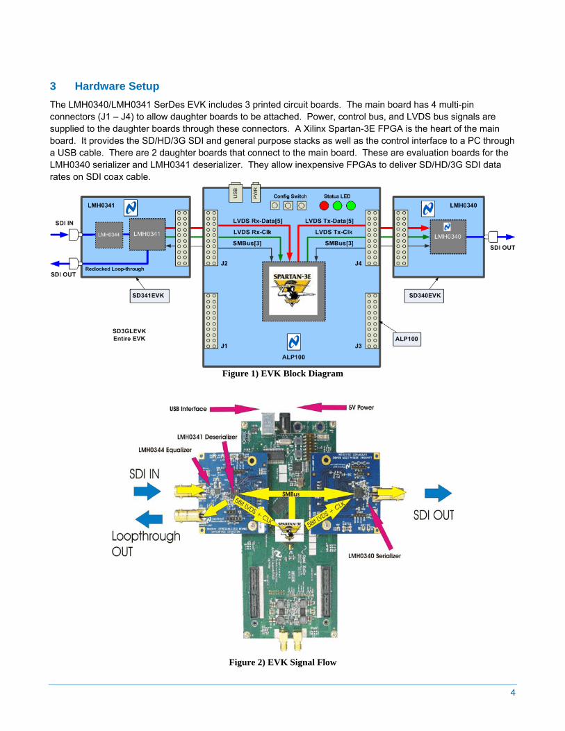
3 Hardware Setup The LMH0340/LMH0341 SerDes EVK includes 3 printed circuit boards. The main board has 4 multi-pin connectors (J1 – J4) to allow daughter boards to be attached. Power, control bus, and LVDS bus signals are supplied to the daughter boards through these connectors. A Xilinx Spartan-3E FPGA is the heart of the main board. It provides the SD/HD/3G SDI and general purpose stacks as well as the control interface to a PC through a USB cable. There are 2 daughter boards that connect to the main board. These are evaluation boards for the LMH0340 serializer and LMH0341 deserializer. They allow inexpensive FPGAs to deliver SD/HD/3G SDI data rates on SDI coax cable.
Figure 1) EVK Block Diagram
Figure 2) EVK Signal Flow
5
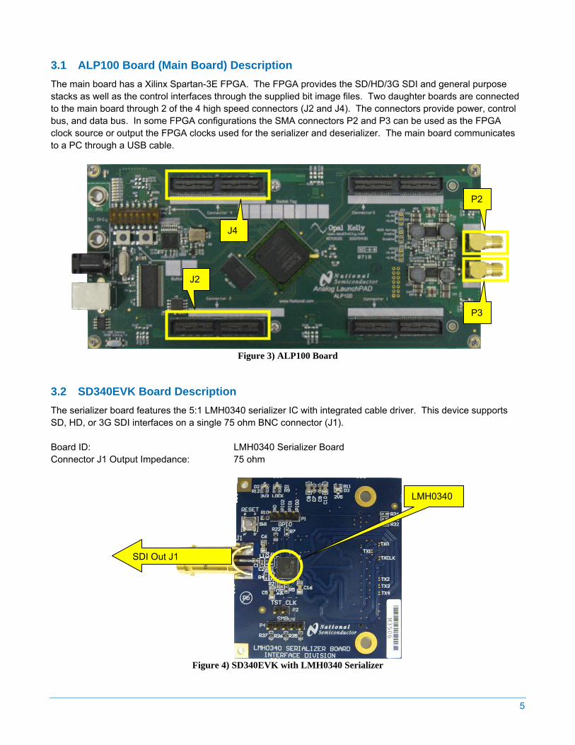
3.1 ALP100 Board (Main Board) Description The main board has a Xilinx Spartan-3E FPGA. The FPGA provides the SD/HD/3G SDI and general purpose stacks as well as the control interfaces through the supplied bit image files. Two daughter boards are connected to the main board through 2 of the 4 high speed connectors (J2 and J4). The connectors provide power, control bus, and data bus. In some FPGA configurations the SMA connectors P2 and P3 can be used as the FPGA clock source or output the FPGA clocks used for the serializer and deserializer. The main board communicates to a PC through a USB cable.
Figure 3) ALP100 Board
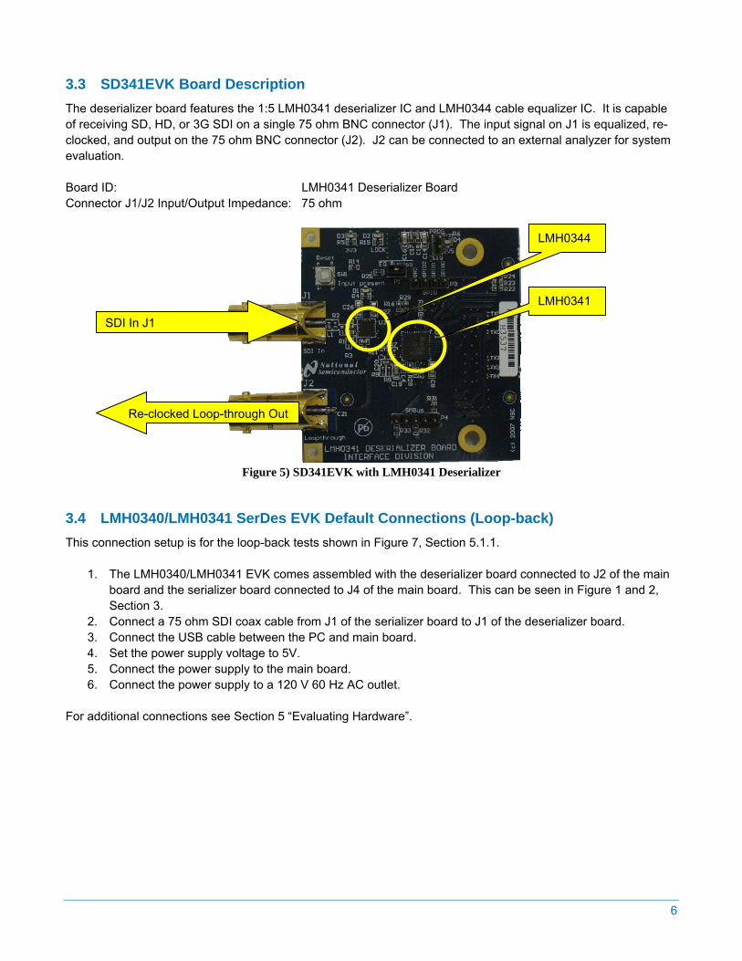
3.2 SD340EVK Board Description The serializer board features the 5:1 LMH0340 serializer IC with integrated cable driver. This device supports SD, HD, or 3G SDI interfaces on a single 75 ohm BNC connector (J1). Board ID: LMH0340 Serializer Board Connector J1 Output Impedance: 75 ohm
Figure 4) SD340EVK with LMH0340 Serializer
J4
J2
LMH0340
SDI Out J1
P2
P3
6
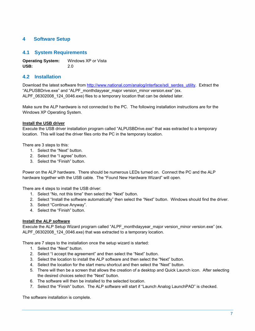
3.3 SD341EVK Board Description The deserializer board features the 1:5 LMH0341 deserializer IC and LMH0344 cable equalizer IC. It is capable of receiving SD, HD, or 3G SDI on a single 75 ohm BNC connector (J1). The input signal on J1 is equalized, re-clocked, and output on the 75 ohm BNC connector (J2). J2 can be connected to an external analyzer for system evaluation. Board ID: LMH0341 Deserializer Board Connector J1/J2 Input/Output Impedance: 75 ohm
Figure 5) SD341EVK with LMH0341 Deserializer
3.4 LMH0340/LMH0341 SerDes EVK Default Connections (Loop-back) This connection setup is for the loop-back tests shown in Figure 7, Section 5.1.1.
1. The LMH0340/LMH0341 EVK comes assembled with the deserializer board connected to J2 of the main board and the serializer board connected to J4 of the main board. This can be seen in Figure 1 and 2, Section 3.
2. Connect a 75 ohm SDI coax cable from J1 of the serializer board to J1 of the deserializer board. 3. Connect the USB cable between the PC and main board. 4. Set the power supply voltage to 5V. 5. Connect the power supply to the main board. 6. Connect the power supply to a 120 V 60 Hz AC outlet.
For additional connections see Section 5 “Evaluating Hardware”.
Re-clocked Loop-through Out
LMH0344
LMH0341
SDI In J1
7
4 Software Setup
4.1 System Requirements Operating System: Windows XP or Vista USB: 2.0
4.2 Installation Download the latest software from http://www.national.com/analog/interface/sdi_serdes_utility. Extract the “ALPUSBDrive.exe” and “ALPF_monthdayyear_major version_minor version.exe” (ex. ALPF_06302008_124_0046.exe) files to a temporary location that can be deleted later. Make sure the ALP hardware is not connected to the PC. The following installation instructions are for the Windows XP Operating System. Install the USB driver Execute the USB driver installation program called “ALPUSBDrive.exe” that was extracted to a temporary location. This will load the driver files onto the PC in the temporary location. There are 3 steps to this:
1. Select the “Next” button. 2. Select the “I agree” button. 3. Select the “Finish” button.
Power on the ALP hardware. There should be numerous LEDs turned on. Connect the PC and the ALP hardware together with the USB cable. The “Found New Hardware Wizard” will open. There are 4 steps to install the USB driver:
1. Select “No, not this time” then select the “Next” button. 2. Select “Install the software automatically” then select the “Next” button. Windows should find the driver. 3. Select “Continue Anyway”. 4. Select the “Finish” button.
Install the ALP software Execute the ALP Setup Wizard program called “ALPF_monthdayyear_major version_minor version.exe” (ex. ALPF_06302008_124_0046.exe) that was extracted to a temporary location. There are 7 steps to the installation once the setup wizard is started:
1. Select the “Next” button. 2. Select “I accept the agreement” and then select the “Next” button. 3. Select the location to install the ALP software and then select the “Next” button. 4. Select the location for the start menu shortcut and then select the “Next” button. 5. There will then be a screen that allows the creation of a desktop and Quick Launch icon. After selecting
the desired choices select the “Next” button. 6. The software will then be installed to the selected location. 7. Select the “Finish” button. The ALP software will start if “Launch Analog LaunchPAD” is checked.
The software installation is complete.
8
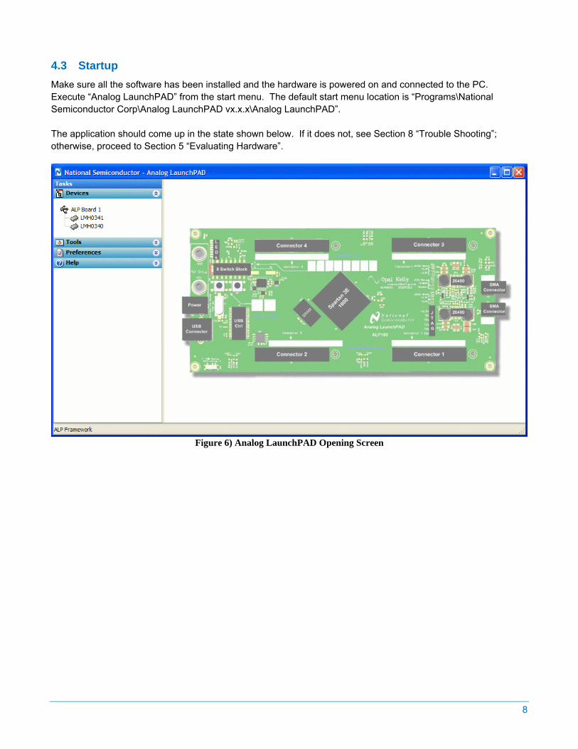
4.3 Startup Make sure all the software has been installed and the hardware is powered on and connected to the PC. Execute “Analog LaunchPAD” from the start menu. The default start menu location is “Programs\National Semiconductor Corp\Analog LaunchPAD vx.x.x\Analog LaunchPAD”. The application should come up in the state shown below. If it does not, see Section 8 “Trouble Shooting”; otherwise, proceed to Section 5 “Evaluating Hardware”.
Figure 6) Analog LaunchPAD Opening Screen
9
5 Evaluating Hardware The EVK is designed for flexible and accurate evaluation of LMH0340 and LMH0341. Evaluation can be performed using internal or external stimuli and monitoring devices. There is an internal pattern generator implemented in the FPGA that will generate test patterns to verify signal transmission and signal integrity. The pattern generator can generate various types of patterns including standard PRBS patterns, SD/HD/3G SDI static video patterns, and user defined statically repeating patterns. The internal BERT or external test equipment can be used to do a thorough evaluation of the EVK.
5.1 Test Setups
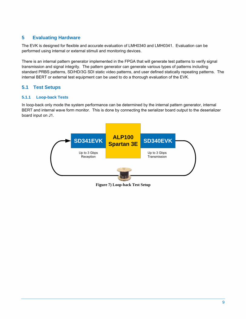
5.1.1 Loop-back Tests
In loop-back only mode the system performance can be determined by the internal pattern generator, internal BERT and internal wave form monitor. This is done by connecting the serializer board output to the deserializer board input on J1.
ALP100Spartan 3E
Up to 3 GbpsReception
Up to 3 GbpsTransmission
SD341EVK SD340EVK
Figure 7) Loop-back Test Setup
10
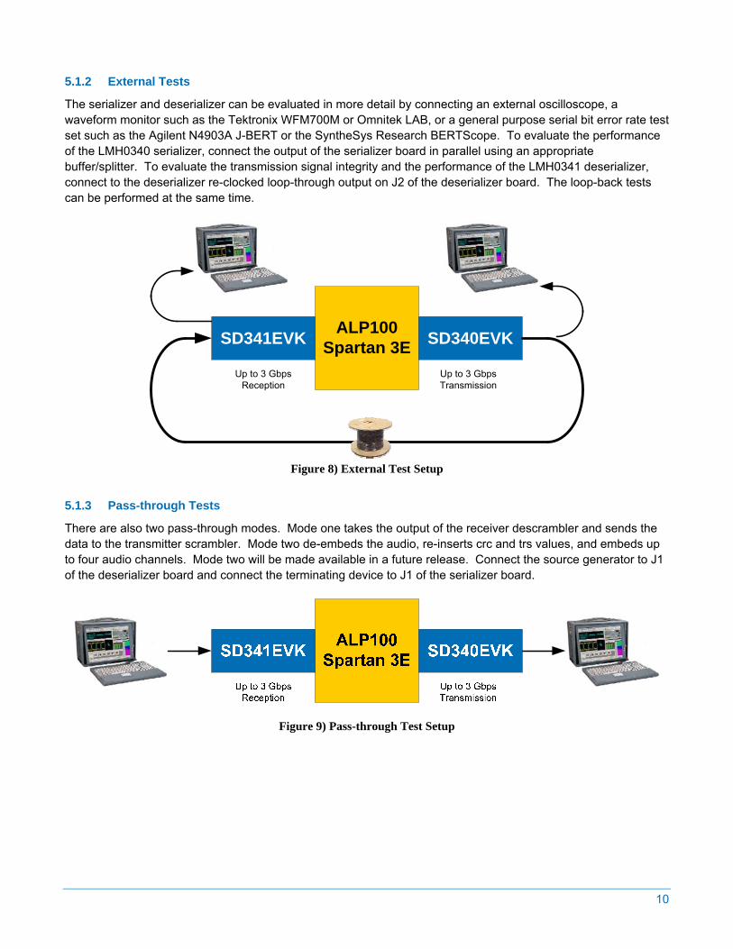
5.1.2 External Tests
The serializer and deserializer can be evaluated in more detail by connecting an external oscilloscope, a waveform monitor such as the Tektronix WFM700M or Omnitek LAB, or a general purpose serial bit error rate test set such as the Agilent N4903A J-BERT or the SyntheSys Research BERTScope. To evaluate the performance of the LMH0340 serializer, connect the output of the serializer board in parallel using an appropriate buffer/splitter. To evaluate the transmission signal integrity and the performance of the LMH0341 deserializer, connect to the deserializer re-clocked loop-through output on J2 of the deserializer board. The loop-back tests can be performed at the same time.
ALP100Spartan 3ESD341EVK SD340EVK
Up to 3 GbpsReception
Up to 3 GbpsTransmission
Figure 8) External Test Setup
5.1.3 Pass-through Tests
There are also two pass-through modes. Mode one takes the output of the receiver descrambler and sends the data to the transmitter scrambler. Mode two de-embeds the audio, re-inserts crc and trs values, and embeds up to four audio channels. Mode two will be made available in a future release. Connect the source generator to J1 of the deserializer board and connect the terminating device to J1 of the serializer board.
Figure 9) Pass-through Test Setup
11
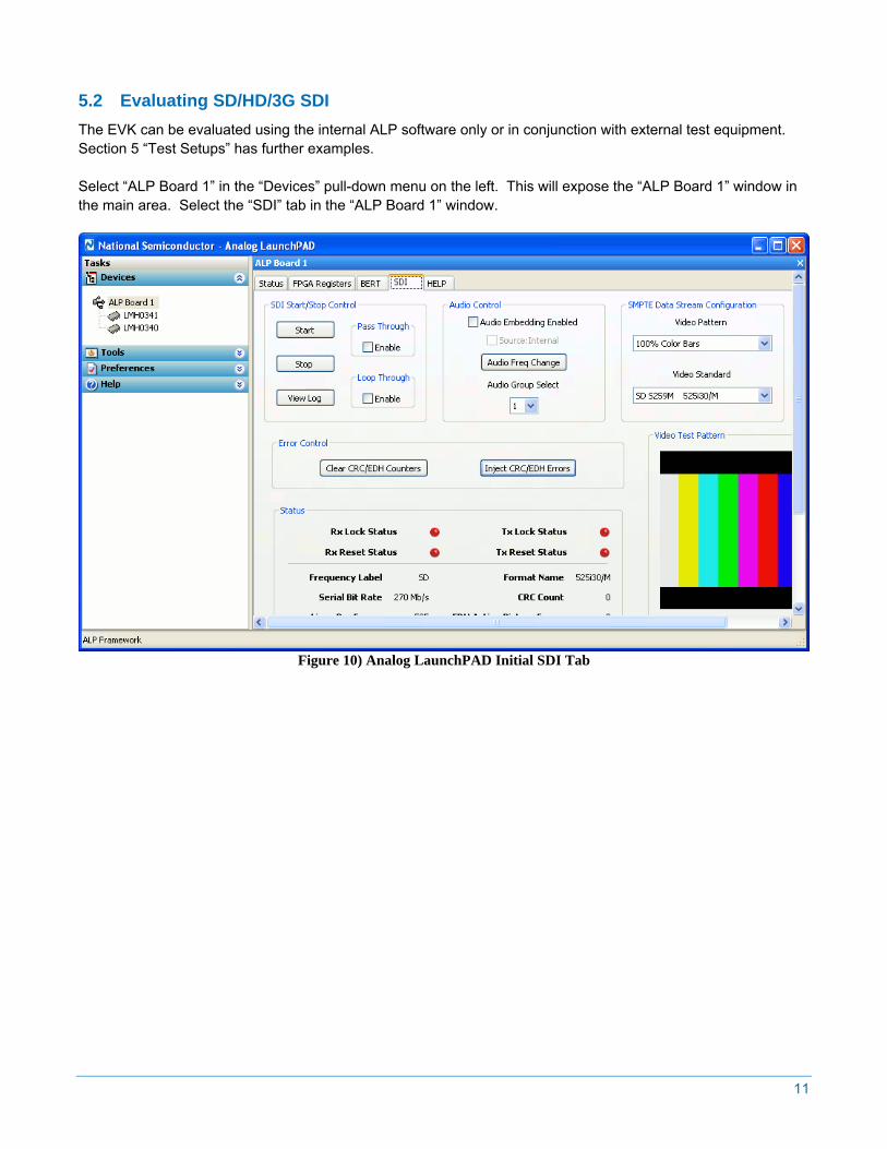
5.2 Evaluating SD/HD/3G SDI The EVK can be evaluated using the internal ALP software only or in conjunction with external test equipment. Section 5 “Test Setups” has further examples. Select “ALP Board 1” in the “Devices” pull-down menu on the left. This will expose the “ALP Board 1” window in the main area. Select the “SDI” tab in the “ALP Board 1” window.
Figure 10) Analog LaunchPAD Initial SDI Tab
12
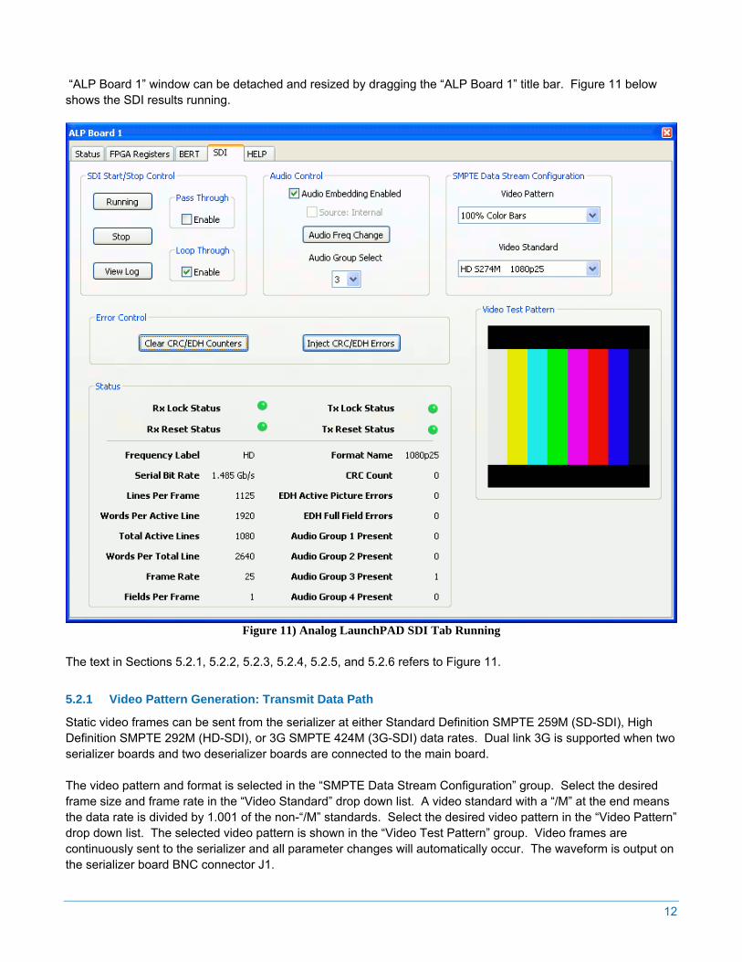
“ALP Board 1” window can be detached and resized by dragging the “ALP Board 1” title bar. Figure 11 below shows the SDI results running.
Figure 11) Analog LaunchPAD SDI Tab Running
The text in Sections 5.2.1, 5.2.2, 5.2.3, 5.2.4, 5.2.5, and 5.2.6 refers to Figure 11.
5.2.1 Video Pattern Generation: Transmit Data Path
Static video frames can be sent from the serializer at either Standard Definition SMPTE 259M (SD-SDI), High Definition SMPTE 292M (HD-SDI), or 3G SMPTE 424M (3G-SDI) data rates. Dual link 3G is supported when two serializer boards and two deserializer boards are connected to the main board. The video pattern and format is selected in the “SMPTE Data Stream Configuration” group. Select the desired frame size and frame rate in the “Video Standard” drop down list. A video standard with a “/M” at the end means the data rate is divided by 1.001 of the non-“/M” standards. Select the desired video pattern in the “Video Pattern” drop down list. The selected video pattern is shown in the “Video Test Pattern” group. Video frames are continuously sent to the serializer and all parameter changes will automatically occur. The waveform is output on the serializer board BNC connector J1.
13
Clicking the “Start” button in the “SDI Start/Stop Control” group will start updates of the status information in the “Status” group. This button label will change to “Initializing” and then “Running”. Click “Stop” to stop the updates of the status information. “Status” group shows the following transmit information:
Tx Lock Status: green if signal present at input to serializer and serializer is locked to signal Tx Reset Status: green if serializer is not in reset
All other information in the “Status” group is receiver information and is covered in Section 5.2.3.
5.2.2 Embeded Audio Generation: Transmit Data Path
Audio can be embedded in the SMPTE 291M ancillary data. One of four SMPTE 299M audio groups can be embedded at a time. Each group contains four audio tones. 3G audio will be supported when the relevant SMPTE standard is finalized. All audio controls are located in the control labeled “Audio Control” group. If the “Audio Embedding Enabled” check box is selected, four tones will be embedded in the group selected in the “Audio Group Select” drop down list. The frequency of the tones can be changed by clicking the “Audio Freq Change” button. If a LM49350 board and break out board is connected to J1 of the ALP100, audio can be externally embedded/deembedded by checking the “Source:Internal” check box. This check box label shows the source of the embedded audio.
5.2.3 Video Format Detect, Audio Detect, CRC and EDH Check: Receive Data Path
The LMH0341 on the deserializer board can receive and deserialize data at SD/HD/3G SDI data rates. The FPGA firmware can detect SMPTE 259M (SD-SDI), SMPTE 292M (HD-SDI), or SMPTE 424M (3G-SDI) video frames as well as SMPTE 299M embedded audio. Connect a standard SD, HD, or 3G SDI video source to the deserializer board BNC connector J1. The “Status” group contains all the received video and audio information. As mentioned in Section 5.2.1, the “Start” button in the “SDI Start/Stop Control” group must show “Running” or the status information is not updating. “Status” group shows the receiver information:
Rx Lock Status: green if signal present at input to deserializer and deserializer is locked to signal Rx Reset Status: green if deserializer is not in reset
Serial Bit Rate: serial bit rate of recovered serial data Lines Per Frame: total number of lines per frame Words Per Active Line: number of video samples per active line Total Active Lines: number of active lines per frame
Words Per Total Line: number of samples per line including header, video, and ancillary data Frame Rate: number of frames per second Fields Per Frame: 1 for progressive scanning or 2 for interlaced scanning Frequency Label: SD, HD, HD/M, 3G, or 3G/M (/M indicates divide by 1.001) Format Name: short name for video format (lines per active frame, scanning format, fame rate) CRC Errors: accumulated luma (Y) and chroma (CB and CR) CRC errors (HD and 3G) EDH Active Picture Errors: accumulated active picture errors (SD) EDH Full Field Errors: accumulated full field errors, includes active picture errors (SD) Audio Group 1 Present: embedded audio group 1 present if value is 1 Audio Group 2 Present: embedded audio group 2 present if value is 1
14
Audio Group 3 Present: embedded audio group 3 present if value is 1 Audio Group 4 Present: embedded audio group 4 present if value is 1
5.2.4 Deserializer Re-clocked Loop-through: Receive Data Path
The deserializer has a re-clocked loop-through output with cable driver. This is the clock recovered version of the signal present at the input to the deserializer. This feature is useful for sending a clean SDI signal to additional equipment. Enable the deserializer re-clocked loop-through mode by checking the “Enable” check box in the “Loop Through” group.
5.2.5 Pass-through: Receive, Transmit Data Path
There is a pass-through mode on the “SDI” tab. In pass-through mode the signal at the output of the receiver descrambler is sent to the input transmitter scrambler. As long as the deserializer can recover the clock, the signal will be passed through to the output of the serializer even if the signal is not recognized as a standard video format. Enable pass-through mode by checking the “Enable” check box in the “Pass Through” group. The FPGA firmware and ALP software still has the capability to analyze the video frames and embedded audio coming from the deserializer.
15
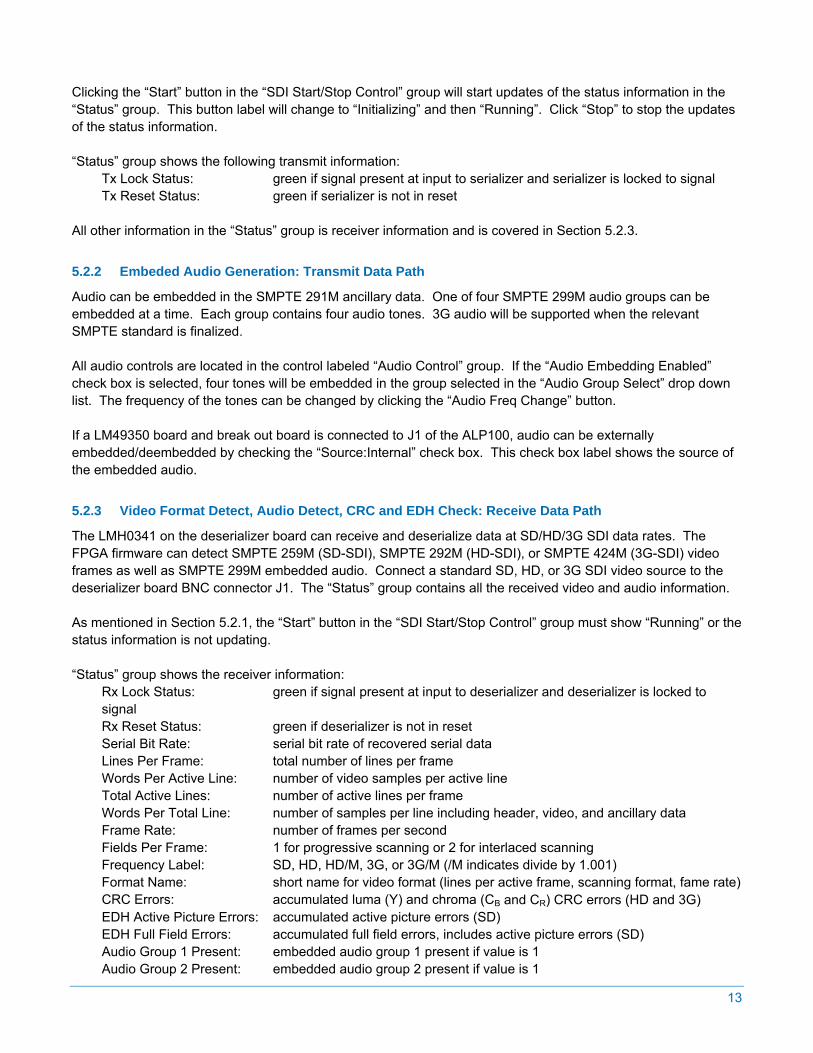
5.3 Evaluating Using Bit Error Rate Tester Engine The EVK can be evaluated using the internal ALP software only or in conjunction with external test equipment. Section 5 “Test Setups” contains further examples. This section describes the usage of the ALP software with the internal Bit Error Rate Tester (BERT) engine. Select “ALP Board 1” in the “Devices” pull-down menu on the left. This will expose the “ALP Board 1” window in the main area. Select the “BERT” tab in the “ALP Board 1” window.
Figure 12) Analog LaunchPAD Initial BERT Tab
16
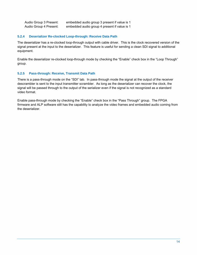
“ALP Board 1” window can be detached and resized by dragging the “ALP Board 1” title bar. Figure 13 below shows the BERT running.
Figure 13) Analog LaunchPAD BERT Tab Running
The text in Sections 5.3.1, 5.3.2, 5.3.3, 5.3.4, and 5.3.5 refers to Figure 13.
5.3.1 Data Pattern Generation: Transmit Data Path
The “BERT” tab can be used to send test patterns to the serializer at 270 Mbps, 1.5 Gbps or 3 Gbps. Select the desired pattern and whether SMPTE scrambling and NRZI is on in the “BERT Pattern Select” group. Select the desired data rate in the “Serial Bit Rate Configuration” group. When using a fixed pattern, the “Scramble/NRZI” check box may need to be checked in order for the deserializer to recover the clock. “Scramble/NRZI” should normally be checked. Click the “Start” button in the “BERT Control” group to send the selected pattern to the serializer. This button also shows the current status. After clicking the button it will read “Init” and then “Running”. The waveform is output on the serializer board BNC connector J1. If any of the settings in the “BERT Pattern Select” group are changed, click the “Stop” button and then the “Start” button for the change to take effect. “Device Status” group shows the following transmit information:
Tx Lock: green if signal present at input to serializer and serializer is locked to signal
17
5.3.2 Error Injection: Transmit Data Path
Errors can be injected into the transmit data to demonstrate how the link behaves under various conditions. The “BERT Control” group has three buttons that allow error injection. Clicking the “Error” button will inject an error once. Clicking the “Burst Errors” button will inject a burst of errors once. Clicking the “Inject Errors” will continuously inject bursts of errors. It will make the BERT look as though it is unlocked due to the high number of errors. The “Inject Errors” button must be clicked again to stop the errors.
5.3.3 Data Pattern Verification: Receive Data Path
There is a BERT implemented in the FPGA on the ALP board. The BERT will try to lock to the pattern matching the settings in the “BERT” tab. Start the BERT by clicking the “Start” button in the “BERT Control” group. If the input signal on J1 of the deserializer board matches the settings in the “BERT” tab, the counters in the “BERT Status” group will accumulate. The counters can be cleared by clicking the “Clear Counters” button in the “BERT Control” group. There is also a graph that shows the bit errors vs. time in seconds. The plot can be shown by clicking the “Plot Errors” button. “Device Status” group and “BERT Status” group shows the following receiver information:
Rx Lock: green if signal present at input to deserializer and deserializer is locked to signal Running: green if BERT is running
Locked: green if BERT can lock to input data pattern No Errors: green if no bit errors have accumulated Bit Count: total bits accumulated x 106 (un-errored + errored bits) Errors: errored bits accumulated
Ratio: ratio of Errors over Bit Count (bit error rate)
5.3.4 Deserializer Re-clocked Loop-through: Receive Data Path
The deserializer has a re-clocked loop-through output with cable driver. This is the clock recovered version of the signal present at the input to the deserializer. This feature is useful for sending a clean SDI signal to additional equipment. Enable the deserializer re-clocked loop-through mode by checking the “Loop Through” check box in the “BERT Pattern Select” group.
5.3.5 External Clock I/O
The SMA connectors P2 and P3 can be used to drive or monitor the 1x clock of the FPGA serializer data path or monitor the 1x clock of the FPGA deserializer data path. The 1x clock is 1/20 of the serial clock rate. P2 is the clock input connector and P3 is the clock output connector. The function of P2 and P3 is selected by the radio buttons in the “External Clock Control” group. When switching between the “LMK3000C” and “SMA Conn P2” radio buttons the BERT must be stopped and restarted.
18
6 Documentation Additional LMH0340/LMH0341 EVK documentation can be found at http://www.national.com/analog/interface/sdi_serdes_utility.
6.1 Schematics, BOMs, and Data Sheets All of the schematics and BOMs for the LMH0340/LMH0341 EVK can be found at the above URL. The datasheets can be found at http://www.national.com/sdi. There is also information for other SDI parts at this URL. Note: The BOM for the ALP100 board is not available.
6.2 Reference FPGA IP The reference FPGA IP source code and documentation will be made available after signing a Software License Agreement. Please speak to a National Semiconductor representative for more details.
7 Part Numbers Serializer Board: SD340EVK Deserializer Board: SD341EVK Analog LaunchPAD Board: ALP100 LMH0340/LMH0341 Evaluation Kit: SD3GXLEVK
19
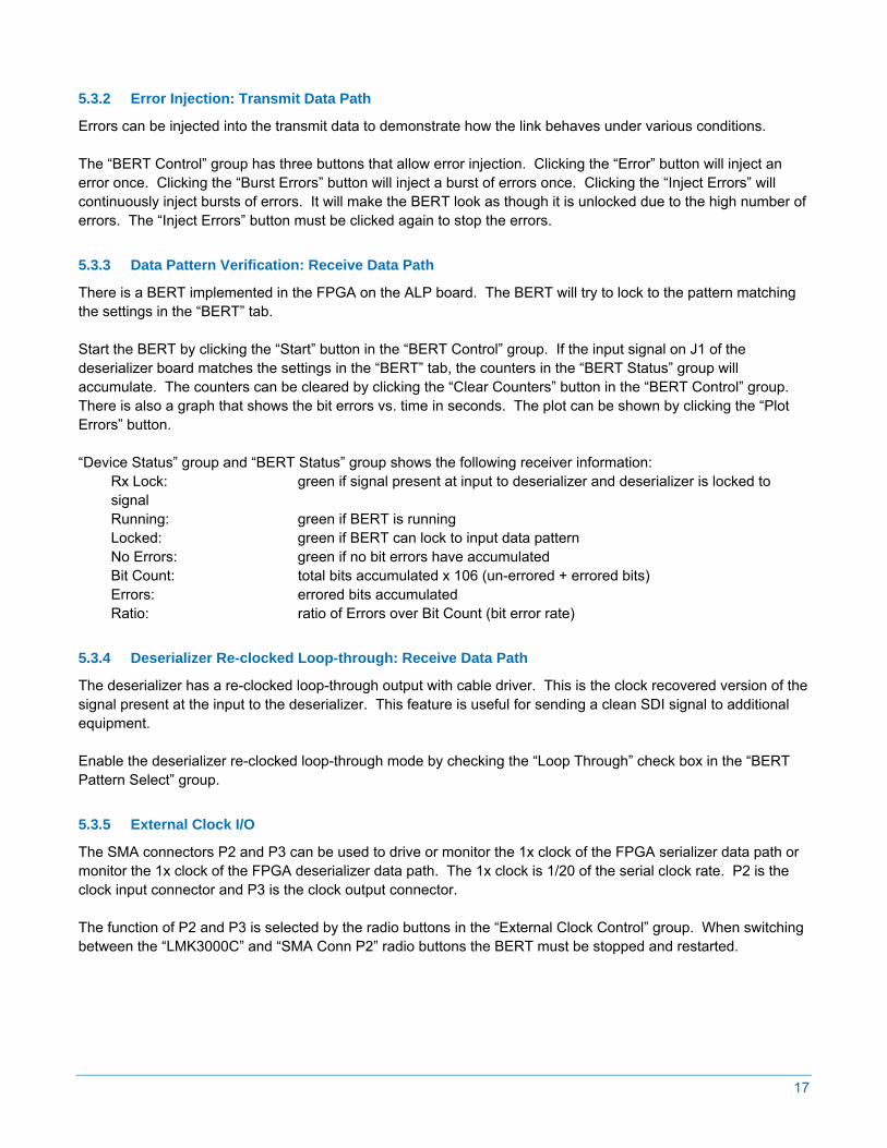
8 Trouble Shooting If the following window opens after starting the ALP software double check the hardware setup.
Figure 14) Analog LaunchPAD No Devices Error
It may also be that the USB driver is not installed. Check the device manager. There should be an ”Opal Kelly XEM3020” device under the “Universal Serial Bus Controllers” as shown below in Figure 15.
Figure 15) Windows XP, Analog LauchPAD USB Driver
20
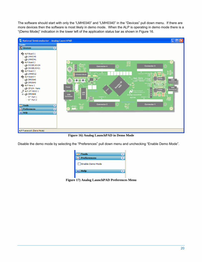
The software should start with only the “LMH0340” and “LMH0340” in the “Devices” pull down menu. If there are more devices then the software is most likely in demo mode. When the ALP is operating in demo mode there is a “(Demo Mode)” indication in the lower left of the application status bar as shown in Figure 16.
Figure 16) Analog LaunchPAD in Demo Mode
Disable the demo mode by selecting the “Preferences” pull down menu and unchecking “Enable Demo Mode”.
Figure 17) Analog LaunchPAD Preferences Menu
21
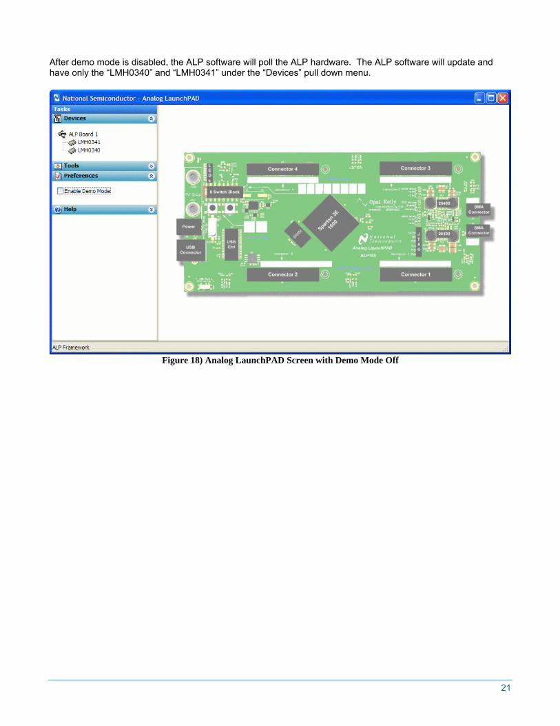
After demo mode is disabled, the ALP software will poll the ALP hardware. The ALP software will update and have only the “LMH0340” and “LMH0341” under the “Devices” pull down menu.
Figure 18) Analog LaunchPAD Screen with Demo Mode Off


