., ;, ' . Recent Total Ionizing Dose and Displacement Damage Compendium of Candidate Electronics for NASA Space Systems Donna J. Cochran'. Alvin J. Boutte 2 , Michael J. Campola 2 , Martin A. Carts 2 , Megan C. Case/ , Dakai Chen 2 , Kenneth A. LaBei2, Raymond L. Ladbury2, Jean-Marie Lauenstein 2 , Cheryl J. Marshall 2 , Martha V. O'Bryan1, T imothy R. Oldham3, Jonathan A. Pellish 2 , Anthony B. Sanders 2 , and Michael A. Xapsos 2 I. MEI Technologies, Inc., Seabrook, MD 20706 USA 2. NASA Goddard Space Flight Center (GSFC), Code 561.4, Greenbelt, MD 20771 USA 3. Dell Perot Systems Inc., Fairfax, VA 22031 USA Abstract-· Vulnerability of a variety of candidate spacecraft electronics to total ionizing dose and displace ment damage is studied. Devices tested include o ptoelectronics, digital, analog, linear bipolar devices, and hy brid devices. Index Terms- Displacement Damage, Optoelectronics, Proton Damage, Single Event Effects, and Total Ionizing Dose. I. INTRODUCTION NASA spacecraft are subjected to a harsh space environment that includes exposure to various types of ionizing radiation. .Long-term exposure to radiation has been known to affect the function of the spacecraft electronics. As a result flight parts must be tolerant to radiation-induced Total Ionizing Dose (TIO) and displacement damage (DD) effects for space approval or parts must be mitigated by shielding or other methods to reduce TIO effects. Hence, the effects of TIO and proton DD need to be evaluated by test in order to determine risk to space projects. The test results presented here were gathered to establish the sensitivity of candidate spacecraft electronics to TIO and/or proton damage. For similar results on single event effects (SEE), a companion paper has also been submitted to the 201 1 IEEE NSREC Radiation Effects Data Workshop entitled: "Recent Single Event Effects Compendium of This work was supported in part by the NASA Electronic Parts and Packaging Program (NEPP), NASA Flight Proj ects, and the Defense Threat Reduction Agency (DTRA) under lACRO# I 0-49771 and l l-43951. Donna J. Cochran, MEI Technologies Inc., work performed for NASA Goddard Space Flight Center, Code 561.4, Greenbelt, MD 20771 (USA), phone: 301 -286-8258, fax : 301 - 286-4699, email: DonnaJ.Cochran@nasagov. Jonathan A. Pellish, NASA/GSFC, Code 561.4, Greenbelt, MD 20771 (USA), phone: 301-286-6523, email: Jonathan.A.[email protected]ov. Megan C. Casey, NASA/GSFC, Code 561.4, Greenbelt, MD 20771 (USA), phone: 301-286-11 SI, email: Megan.C.Case [email protected]. Raymond L. Ladbury, NASA/GSFC, Code 561.4, Greenbelt, MD 20771 (USA), phone: 301-286-1030, email: Raymond.L.Ladbury@nasa.gov. Timothy R. Oldham, Dell Perot Syste ms Government Services, Inc., work performed for NASA Goddard Space Flight Center, Code 561.4, Greenbelt, MD 20771 (USA), phone: 301-286-5489, email: Timothy.R.Oldham@nasagov. Martha V. O'Bryan is with MEI Technologies Inc., work performed for NASA Goddard Space Flight Center, Code 561.4, Greenbelt, MD 20771 (USA), phone: 301-286-131 2, email: Martha. V.Obryan@nasagov. Alvin Boutte, Michael J. Campola, Martin A. Carts, Dakai Chen, Kenneth A. LaBel, Cheryl J. Marshall, Jean-Marie Lauenstein, Anthony B. Sanders.and Michael Xapsos are with NASA/GSFC, Code 561.4, Greenbelt, MD 20771 (USA), phone:301-286-8046 (Sanders ), 301-286-9936 (LaBel), email : Anthony.B. [email protected], Kenneth.A.LaBel@nasa.gov. Candidate Electronics for NASA Space Systems" by M. O'Bryan, et al. [I] II. TEST TECHNIQUES ANO SETUP Unless otherwise noted, all tests were performed at room temperature and with nominal power supply voltages. A. Test Methods- TJD T IO testing was performed using a Co-60 source. Dose rates used fo r testing were between 0.0005 and 50 rads(Si)/s. B. Test Methods - Proton Proton DDffIO tests were performed at the University of California at Davis • Crocker Nuclear Laboratory (UCD- CNL) using a 76" cyclotron (maximum energy of 63 MeV) and the Lawrence Berkeley National Laboratory (LBNL) Berkeley Accelerator Space Effects (BASE). Table I lists the proton damage test facilities and energies used on the devices. TABLE I PROTON TEST FACILI TIES Facility Proton Energy, (McV) University of California at Davis - 6.5-63 Crocker Nuclear Laboratory (UCD-CNL) Lawrence Berkeley National Laboratory (LBNL) Berkeley Accelerator Space Effects so (BASE) C. Test Meth ods- Electron Electron DDffIO tests were performed at Rensselaer Polytechnic Institute's (RPI) Gaerttner Linear Accelerator Laboratory. The electron energies used were between 5 and 50MeV. lll. TESTRESULTS0VERVIEW · Abbreviations for principal investigators (Pls) are listed in Table II. Abbreviations and conventions are listed in Table III. Please note that these test results can depend on operational conditions. Complete test reports are available online at http://radhome.gsfc.nasa.gov [3]. To be presented by Alvin Boutte at the International Electrical and Electronics Engineering (IEEE) Nuclear and Space Radiation Effects Conference (NSREC), July 27, 2011, Las Vegas, NV, and.published on nepp.nasa.gov and radhome.gsfc.nasa.gov. I .. ---
Transcript
.,
;, ' .
Recent Total Ionizing Dose and Displacement Damage Compendium of Candidate Electronics for NASA Space Systems
Donna J. Cochran'. Alvin J. Boutte2, Michael J. Campola2
, Martin A. Carts2, Megan C. Case/, Dakai Chen2
,
Kenneth A. LaBei2, Raymond L. Ladbury2, Jean-Marie Lauenstein2, Cheryl J. Marshall2,
Martha V. O'Bryan1, Timothy R. Oldham3, Jonathan A. Pellish2, Anthony B. Sanders2, and Michael A. Xapsos2
I. MEI Technologies, Inc., Seabrook, MD 20706 USA 2. NASA Goddard Space Flight Center (GSFC), Code 561.4, Greenbelt, MD 20771 USA
3. Dell Perot Systems Inc., Fairfax, VA 22031 USA
Abstract-· Vulnerability of a variety of candidate spacecraft electronics to total ionizing dose and displacement damage is studied. Devices tested include optoelectronics, digital, analog, linear bipolar devices, and hybrid devices.
Index Terms- Displacement Damage, Optoelectronics, Proton Damage, Single Event Effects, and Total Ionizing Dose.
I. INTRODUCTION
NASA spacecraft are subjected to a harsh space environment that includes exposure to various types of ionizing radiation . . Long-term exposure to radiation has been known to affect the function of the spacecraft electronics. As a result flight parts must be tolerant to radiation-induced Total Ionizing Dose (TIO) and displacement damage (DD) effects for space approval or parts must be mitigated by shielding or other methods to reduce TIO effects. Hence, the effects of TIO and proton DD need to be evaluated by test in order to determine risk to space projects.
The test results presented here were gathered to establish the sensitivity of candidate spacecraft electronics to TIO and/or proton damage. For similar results on single event effects (SEE), a companion paper has also been submitted to the 201 1 IEEE NSREC Radiation Effects Data Workshop entitled: "Recent Single Event Effects Compendium of
This work was supported in part by the NASA Electronic Parts and Packaging Program (NEPP), NASA Flight Projects, and the Defense Threat Reduction Agency (DTRA) under lACRO# I 0-49771 and l l-43951.
Donna J. Cochran, MEI Technologies Inc., work performed for NASA Goddard Space Flight Center, Code 561.4, Greenbelt, MD 20771 (USA), phone: 301-286-8258, fax: 301-286-4699, email: DonnaJ.Cochran@nasagov.
Jonathan A. Pellish, NASA/GSFC, Code 561.4, Greenbelt, MD 20771 (USA), phone: 301-286-6523, email: [email protected].
Raymond L. Ladbury, NASA/GSFC, Code 561.4, Greenbelt, MD 20771 (USA), phone: 301-286-1030, email: [email protected].
Timothy R. Oldham, Dell Perot Systems Government Services, Inc., work performed for NASA Goddard Space Flight Center, Code 561.4, Greenbelt, MD 20771 (USA), phone: 301-286-5489, email: Timothy.R.Oldham@nasagov.
Martha V. O'Bryan is with MEI Technologies Inc., work performed for NASA Goddard Space Flight Center, Code 561.4, Greenbelt, MD 20771 (USA), phone: 301-286-1312, email: Martha. V.Obryan@nasagov.
Alvin Boutte, Michael J. Campola, Martin A. Carts, Dakai Chen, Kenneth A. LaBel, Cheryl J. Marshall, Jean-Marie Lauenstein, Anthony B. Sanders.and Michael Xapsos are with NASA/GSFC, Code 561.4, Greenbelt, MD 20771 (USA), phone:301-286-8046 (Sanders), 301-286-9936 (LaBel), email: [email protected], [email protected].
Candidate Electronics for NASA Space Systems" by M. O'Bryan, et al. [I]
II. TEST TECHNIQUES ANO SETUP
Unless otherwise noted, all tests were performed at room temperature and with nominal power supply voltages.
A. Test Methods- TJD
TIO testing was performed using a Co-60 source. Dose rates used for testing were between 0.0005 and 50 rads(Si)/s.
B. Test Methods - Proton
Proton DDffIO tests were performed at the University of California at Davis • Crocker Nuclear Laboratory (UCDCNL) using a 76" cyclotron (maximum energy of 63 MeV) and the Lawrence Berkeley National Laboratory (LBNL) Berkeley Accelerator Space Effects (BASE). Table I lists the proton damage test facilities and energies used on the devices.
TABLE I PROTON TEST FACILITIES
Facility Proton Energy, (McV)
University of California at Davis -6.5-63 Crocker Nuclear Laboratory (UCD-CNL)
Lawrence Berkeley National Laboratory (LBNL) Berkeley Accelerator Space Effects so (BASE)
C. Test Methods- Electron
Electron DDffIO tests were performed at Rensselaer Polytechnic Institute's (RPI) Gaerttner Linear Accelerator Laboratory. The electron energies used were between 5 and 50MeV.
lll. TESTRESULTS0VERVIEW
· Abbreviations for principal investigators (Pls) are listed in Table II. Abbreviations and conventions are listed in Table III. Please note that these test results can depend on operational conditions. Complete test reports are available online at http://radhome.gsfc.nasa.gov [3].
To be presented by Alvin Boutte at the International Electrical and Electronics Engineering (IEEE) Nuclear and Space Radiation Effects Conference (NSREC), July 27, 2011, Las Vegas, NV, and.published on nepp.nasa.gov and radhome.gsfc.nasa.gov.
I .. ---
TABLE II LIST OF PRINCIPAL INVESTIOATORS
Abbreviation Principal Investigator (Pl)
MiC Michael Camoola MaC Martin Cans MeC Megan Casey DC DakaiChen RL Ravmond Ladburv
JML Jean-Marie Lauenstein CM Chervl Marshall TO Timothy Oldham JP Jonathan Pellish AS Anthony ITony) Sanders MX Michael Xapsos
TABLE Ill ABBREVIATIONS AND CONVENTIONS
ACRONYM/ DEFINITION ACRONYM/ DEFINITION A=Amp LDR = Low Dose Rate BiCMOS = Bipolar- Complementary Metal Oxide Semiconductor MeV - Mega Electron Volt BIT= Bipolar Junction Transistor mA '" milliamp CERDIP = Ceramic Dip MOSFET .. Metal Oxide Semiconductor Field Effect CMOS = Complementary Metal Oxide Semiconductor NIA = Not Available CTR= Current Transfer Ratio Op-Amp = Operational Amplifier DAC = Digital to Analog Converter P= Proton DC-DC = Direct Current to Direct Current Pl = Principal Investigator DD= Displacement Damage REAG == Radiation Effects & Analysis Group DNL = Differential Non-Linearity RPI= Rensselaer P!'lytechnic Institute Gaerttner Linear Accelerator DTRA = Defense Threat Reduction Agency Laboratory OUT= Device Under Test SEE· Single Event Effects ov...,DI .... = Output Voltage Load Regulation Spec = Specification(s) E = Electron TIO= Total Ionizing Dose
2
ELDRS = Enhanced Low Dose Rate Sensitivity UCD.CNL "' University of California at Davis - Crocker Nuclear Laboratory FET = Field Effect Transistor v_ = Bias Voltage G=Gamma V" = Collector Emitter Voltage GaA!As = Gallium-Aluminum-Arsenide Ve&,,= Collector-Emitter Saturation Voltage GaAsP = Gallium-Arsenide-Phosphide Vm = High Level Input Voltage
HBT = Heterojunction Bipolar Transistor V,. = Voltage In
Hre = Forward Current Transfer Ratio V0, = Offset Voltage
lb= Input Base Vw, = Output Voltage
lbw= Input bias Current V .. ,= Reference Voltage I.,= Collector Current V 1h = Threshold Voltage I.,= Output Current V, = Reverse Breakdown Voltage
IDD = Supply Current 11= Input FO!'Wal'd Current less = Gate Reverse Current Io.= Offset Current InGaP = Indium Gallium Phosphide brr= Output Current IUCF = Indiana University Cyclotron Facility JFET = Junction Field Effect Transistor LBNL BASE= Lawrence Berkeley National Laboratory/Berkeley
Accelerator Space Effects LCC = Lead less Chip Carrier LDC = Lot Date Code LOO = Low Dropout LED = Light Emitting Diode
J
To be presented by Alvin Boutte at the International Electrical and Electronics Engineering (IEEE) Nuclear and Space Radiation Effects Conference (NSREC), July 27,201 I, Las Vegas, NV, and published on nepp.nasa.gov and radhome.gsfc.nasa.gov.
I '' l
11
3
TABLE IV SUMMARY Of TIO AND DD TEsT RESULTS
i:: II)....., ti,...,
Technology/ 0 II) - ..!(? ;:a.C-
, Part Number Manufacturer LDC PI Summary of Results :~ ~ f! :::- u (/)
Device Function 0 (/) ...J '-'
'O 0 "' '-' 'O
~ (/) 0 'O ~] Cl f!
'-' Q'-'
Analoe: Die:ital Converter/Die:ital Analoe: Converter 0827: Functional fai lure was observed in one OUT at 2 krad(Si). 1028: Functional failure observed in one OUT at 10 krad(Si). Both
CMOS I Quad 16-bit 0827 & 1028 show TIO sensitivities to 100, . 0.01 (0827), 2 0 $ X $ 2 (0827); 7 $ X
DAC (0332 & 0409) all tests through 15 krad(Si) at which point 0409) 15 (0332 & 0409)
the biased samples' 100 went out of spec. Both date codes showed no functional failures throueh 20 krad(Si).
AD585 Analog 8440 Bipolar/ MX Droop rate out of spec at 15 krad; V05 at 40 G
IO < droop rate < 15 Devices Sample & Hold Amo krad(Si). • ·
0.01 30 <offset V < 40 · Flash
MT29F8GOAAA WP Micron 0948 CM0S/8G NANO
TO 50 krad(Si). <Fail<75 krad(Si); loss of
Flash erase/write function. G 50 75
K9F8G08UOM Samsung 1031 CMOS/8G NANO TO
400 krad(Si)< Fail<500 krad(Si); partial loss Flash of Erase/Write functions. G 50 500
Miscellaneous LM139AWRQMLV
Natl Semi JM046Xl3 Bipolar/ Analog DC Parameters within spec after 10 krad(Si) for
(1 4-lead CEROIP) Comparator devices irradiated at 0.5 mrad(Si)/s. G 0.0005 >10
HS-1840ARH lntcrsil X0902ABB8 CMOS/ Analog MX Outputs & reference voltage held at G 16.7 >100
Multiolexer application soecific +3.3V.
Ram - 6+ . Mini-Circuits NIA Bipolar / MX
For 2 lots of 8 parts each worst-case·gain G 0.02 >50
RF Amnlifier de1rn1dation at 50 krad was 15%.
ISL74422ARH/1SL4422BRH lntersil 0948 BiCMOS/ RL Minor degradation. All parts within spec to
MOSFET Driver > I 00 krad(Si). G 0.01 >100
MCM2760-4M QTech 0135 Hybrid / Crystal MeC
All parameters stayed within spec limits to 3 G 74 >3000
Oscillator Mrad(Si).
Ooerational Amolifier/ Amolifier Parameters within spec after 100, 70, 50, & 0.01 > 100 30 krad(Si) for devices irradiated. at 10, 5, I, 0.0005 60<Ib<70
LM 158AJRLQMLV Natl Semi 7W4453G019 Bipolar/ & 0.5 mrad(Si), with the exception of I part 0.001 >50
(8-lead CEROIP) Op-Amp DC at 5 mrad(Si)/s, which parametrically failed G after 70 krad(Si). 5 mrad(Si)/s ( I part): 60 < lb < 70 krad(Si). Devices Exhibit dose rate 0.0005 >30
enhancement after 50 krad{Si).
To be presented by Alvin Boutte at the International Electrical and Electronics Engineering (IEEE) Nuclear and Space Radiation Effects Conference (NSREC), July 27, 2011, Las Vegas, NV, and published on nepp.nasa.gov and radhome.gsfc.nasagov.
"
j ,.,
I I
I
Part Number
LMI24AJRQMLV (14-lead CERDIP)
RHIOI3MH (T05 metal can)
RH1013MJ8 (CERDJP)
RH3 IO (Ceramic Flat-8)
OP497BRC
AD648
PAIO
RH1056A
AD524
OP400
Manufacturer! LDC
Natl Semi I 9R5469G019
Linear Technology I0329N9513AI
Linear Technology I0305N0337A
ST Micro
electronics
Analog Devices
Analog Devices
Apex
Linear Technolo_gy_
Analog Devices
Analog Devices
30849A
0946A
9643
0936
0921A
0939A
0204
Power Mosfet/Misc. Power/DC-DC
SiB455EDK
SPT6235MS
LS2805
Vishay
SSDI
Intl Rectifier
BKW9QZ
0624
0536
Technology/ Device Function
Bipolar/ Op-Amp
Bipolar/ Dual Precision
Op-Amp
Bipolar/ Op-Amp
Bipolar/ Op-Amp
Precision Picoampere Input Current Quad/
Op-Amp
Bipolar/ Op-Af!)J)_ Bipolar/ Op-Am~ Bipolar/
JFET Jnj>ut Op-Amp Bipolar /
Instrumentation AmJ)_
Bipolar/ Quad Op-Amp
Power p-type TrenchFET
Ger:,erat Purpose High Voltage/Power NPN
BJT Hybrid /High
Reliability Radiation Hardened DC/DC
Converter
Pl
DC
Summary of Results
Exhibits no dose rate enhancement. Parameters within spec after 10 & 13 krad(Si) for devices irradiated at l O & 0.5 mrad(Si)/s.
DC 1Parameters within spec after 100, 20, & 10 krad(Si) for 5, 1, & 0.5 mrad(Si)/s.
DC 1Parameters within spec after 100, 20, & 10 krad(Si) for 5, 1, & 0.5 mrad(Si)/s.
DC
JP
MeC
MiC
Parameters within spec for parts irradiated at 5 mrad(Si)/s after 5 krad(Si). l mrad(Si)/s irradiation currently in progress. Significant degradation of all measured parameters after 10 krad(Si). Ibias & 10 , & voltage parametric means out of spec by 4 krad(Si), but may be tolerable in a given application. Co-60 low dose rate testin~ The spec for Ibiu & I0 , was exceeded by one biased part at 2 ~d(S"'i)"---. _ ____ _ All devices stayed within spec up to 50 krad(Si).
MX 14 parts tested all within specs at 50 krad(Si).
MX llbiu out of specs at 10 krad(Si).
rb is most sensitive parameter; V 10 second;
C 0 0
:~ ~ -0 0 ~ (/)
G
G
G
G
G
G
G
G
G
RL !all other parameters in specification to > 60 I G krad(Si).
JML
JP
V '!' ~egrades with TIO. Parameters remained I G wrthm spec. Tested with 1. of0.25 & 0.51 A, Vb= 5 V, & V cc= 155.6 V. Mean hre stayed within I G application spec for the duration of the test.
M C IV out decreased below the specified limit e between I 00 & 300 krad(Si) for one part. G
0 ,-. .... -!!! f! C' 0 (/) "' '-' 0 -0 oS
0.01
0.0005
0.005 0.001
0.0005 0.005 0.001 0.0005
0.0005
0.01
0.01
O.ot
0.02
0.02 ~
0.01
4-17
2-20
67.6
-.:;..-. > C,
j~ co~ 0 ... 0 C,
>13
> IO
>100 >20
>10 >100 >20 >10
>5
2.59($5
4
0 < 101 < 2, 0 < lbw < 2
x>50
>50
5 < Ibia, I < l 0
9<lb<l l.5,15<V,o<20
>150
>2xl06
100 < VOUI < 300
To be presented by Alvin Boutte at the International Electrical and Electronics Engineering (IEEE) Nuclear and Space Radiation Effects Conference (NSREC), July 27, 2011, Las Vegas, NV, and published on nepp.nasa.gov and radhome.gsfc.nasa.gov.
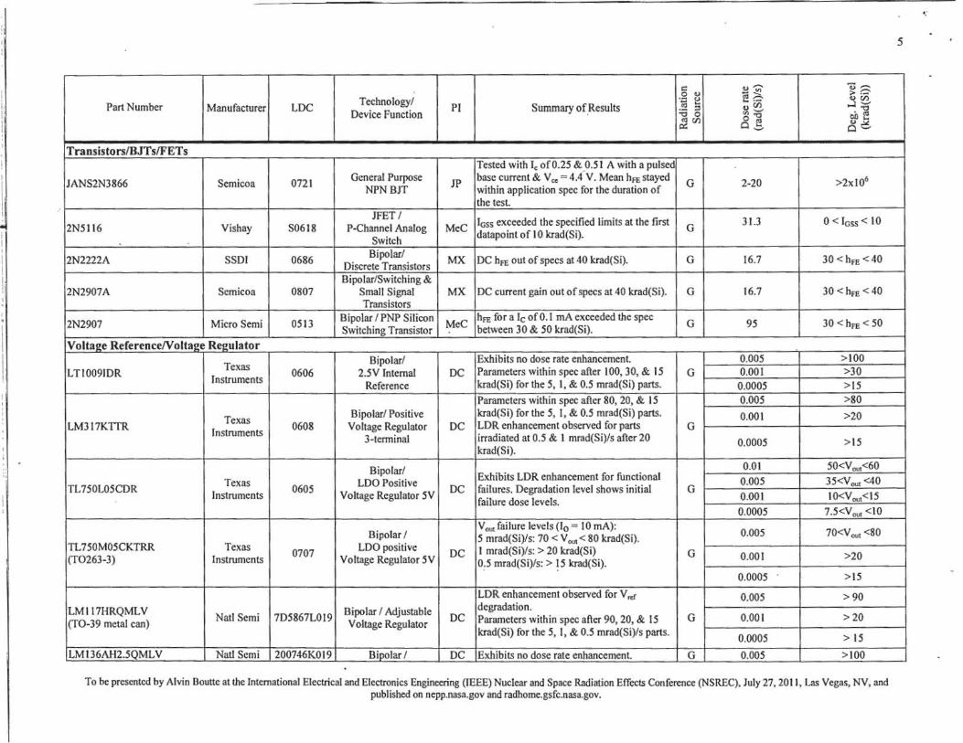
0606 2.5V Internal DC Parameters within spec after I 00, 30, & I 5 G 0.001 >30 Instruments Reference krad(Si) for the 5, l, & 0.5 mrad(Si) parts. 0.0005 >15
Parameters within spec after 80, 20, & I 5 0.005 >80
Texas Bipolar/ Positive krad(Si) for the 5, I, & 0.5 mrad(Si) parts. 0.001 >20
LM317KTIR Instruments 0608 Voltage Regulator DC LDR enhancement observed for parts G
3-tcrrninal irradiated at 0.5 & I mrad(Si)/s after 20 0.0005 > I S krad(Si).
Bipolar/ 0.01 50<V""'<60
Texas LOO Positive Exhibits LOR enhancement for functional 0.005 35<V""' <40
TL750L05CDR Instruments
0605 Voltage Regulator 5V DC failures. Degradation level shows initial G
0707 LOO positive DC I mrad(Si)/s: > 20 krad(Si) G (T0263-3) Instruments Voltage Regulator SY 0:5 mrad(Si)/s: > ! 5 krad(Si).
0.001 >20
0.0005 · >15
LDR enhancement observed for V ,.r 0.005 >90 LM I I 7HRQMLV Bipolar/ Adjustable degradation.
(T0-39 metal can) Natl Semi 7D5867L019 Voltage Regulator DC Parameters within spec after 90, 20, & 15 G 0.00 1 >20 krad(Si) for the 5, I, & 0.5 rnrad(Si)/s parts.
0.0005 > 15
LM136AH2.50MLV Natl Semi 200746KOl9 Bipolar/ DC Exhibits no dose rate enhancement. G 0.005 > 100
To be presented by Alvin Boutte at the International Electrical and Electronics Engineering (IEEE) Nuclear and Space Radiation Effects Conference (NSREC), July 27, 20 11, Las Vegas, NV, and published on nepp.nasa.gov and radhome.gsfc.nasa.gov.
5
j 'I I
I
I I
I I
I i I Iii
1 1
s::: 0 ....... ~8 0 0 -~ Technology/ ·- u e ·- 0 Cl)
Part Number Manufacturer LDC . Pl Summary of Results .a ... 0 Cl) ...l ._.
Device Function ·- ;:I "O "O 0
<ll ._. . "' ~ Cl)
0 "O co ... 0~ u..:.: 0 .......
(3-lead T0-46) 2.5V Reference Parameters w/in spec after 100, 20, & IO 0.001 >20 krad(Si) for the S, I, & 0.5 mrad(Si) devices. o.ooos >IO
RHI021CMW-5 Linear Bipolar/ Precision SY Parameters within spec after I 00, 20, & I 0
o.oos > JOO 0123A Reference DC G 0.001 >20
(Flatpack) Technology krad(Si) for 5, I, & 0.5 mrad(Si)/s. o.ooos >10 0.01 >SO
RHI021CMH-5 Linear Bipolar/ LDR enhancement observed for parts o.oos 80 <V,<90 (TO-Scan) Technology 9783A Precision SV DC irradiated at S mrad(Si)/s after 30 krad(Si). S G
Reference mrad(Si) (T0-5): 90 < V ~ < I 00 krad(Si). 0.001 >20
o.ooos -· >10
Bipolar/ Exhibits dose rate enhancement after IS o.oos 100 <V. <120
RH I009MW Linear krad(Si) for devices irradiated at S & I 0649A 2.SV Reference DC G 0.001 >20 (Flatpack) Technology mrad(Si)/s. S mrad(Si)/s Flatpacks: 100 < V,
< 120 krad(Si). o.ooos >10
Bipolar/ Exhibits dose rate enhancement after 20 o.oos 80 <V,<90 RHI009MH Linear krad(Si) for devices irradiated at S & I (T0-46 can) Technology
0829H 2.SV Reference DC mrad(Si)/s. S mrad(Si)/s T0-46 cans: 80 < V, G 0.001 >20
< 90 krad(Si). o.ooos > 10
RHFIA9 I 3ESY332 ST Bipolar / Parameters within spec for parts irradiated at 0.001 >100
(T02S7) Micro- 30828A Voltage Regulator DC IO, S & I mrad(Si)/s after 100, 30 & 20 G O.OOS >30 electronics k.rad(Si). 0.001 >20
RHFL4913KP332 ST Bipolar / Parameters within spec for parts irradiated at 0.01 > 100
(Flat-1 6) Micro- 30814B Voltage Regulator DC 10, S & I mrad(Si)/s after 100, 30 & 20 G o.oos >30 electronics krad(Si). 0.001 >20
ST Bipolar/ Parameters within spec for parts irradiated at RHF438 (Ceramic Flat-8) Micro- 30820A DC G 0.0005 > 10
electronics Voltage Regulator 0.5 mrad(Si)/s after IO krad(Si).
RI-11021 Linear 0940A
Bipolar/ · V OIi! exceeded the specified limits between I 0 G 55.6 IO<VOll! <30
Technology SY Voltage Reference MeC & 30 krad(Si). ,
To be presented by Alvin Boutte at the International Electrical and Electronics Engineering (IEEE) Nuclear and Space Radiation Effects Conference (NSREC), July 27, 201 1, Las Vegas, NV, and published on nepp.nasagov and radhome.gsfc.nasa.gov.
6
r
II j•I
I
I.I I'
7
Displacement Damage
~ 'vi' - ... C ~0-Technology/ .9 8 f! ?.:- <)N N
Part Number Manufacturer LDC Pl Summary of Results cu ... . ., (/) ..J E E ·- :I Device Function "O 0 "' .._, Cl)~~ 0 "O ~(/) 0 f! U I Q.
....... o.e. Parts remained functional through 2e'' cm'.
4x10¹¹ :5x :5 8xt011 The device CTR dropped out of datasheet
66212 Micropac· !014 GaAIAs/Optocoupler JP specifications between 4xl011 cm·2 & 8xl011 p NIA (Vee = l V);
cm·2 at a Vee of IV & between 8xl011 cm·2 8x I011 :5 x :5 l.2x 1012
& l.2x !012 cm·2 at a V ce of 5 V. Tested with (Vee =5 V) 50 MeV protons. Parts remained functional through 2xt0" 1.2x IO 12 :5 x :5 2x I012 cm·2. CTR within spec at a V ce of 0.4 V for (VcE = 0.1 V);
HCPL-573K Avago 0937 GaAsP/Optocoupler JP all flucnoes tested. CTR out of specification p NIA > 2x10¹² at a Vceof0.1 Vat2xl012 cm·2. Tested with
(V CE = 0.4 V); 50 MeV protons. Parts remained functional & in spec through
RAM-3+ Mini-Circuits 0918 lnGaP/MMIC RF Amp JP 2x!012 cm·2. Mini-Circuits evaluation board p NIA > 2xl012 used for testing. Tested with 50 MeV
. 'protons.
CMOS I Low Voltage Within the measurement resolution & noise UT54LVDSOJ ILV/E Aero flex 0946 MeC threshold, all parameters stayed in spec to a E NIA > 8x!On
Quad Driver 17 McV electron fluence of8 x 1013 cm·2.
MCM2760-4M QTech 0135 Hybrid / Crystal
MeC All parameters stayed within spec limits to a
E NIA > 1.5 X 10¹⁴ Osei llator . 17 MeV electron fluence of 1.5 x 1014 cm·2.
CMOS I Radiation- V1H decreased below the spec between 17 UT54ACS08 Aeroflex 0907 Hardened Quadruple MeC MeV electron fluences of 8 x 10¹³ and l.6 x E NIA 8xl013 :5 X :5 l.6x)014
2-Jnput AND Gates 1014 cm·2. Hybrid /High V out decreased below the specified limit 2.7xl013 $ X $
LS2805 Intl 0536
Reliability Radiation MeC between 17 MeV electron fluences of2.7 and E NIA
Rectifier Hardened DC/DC 5.3 x !On cm·2. 5.3xl013
Converter
JFET / P-Channel Within the measurement resolution & noise
2N5 116 Vishay S0618 MeC threshold, all parameters stayed in spec to a E NIA > 2.7xt014 Analog Switch
17 MeV electron fluence of2.7 x I014 cm·2. hffi for le of 0.1, 1.0, & 10 mA exceeded the l.t xl013 $ X $ spec between 5 MeV electron fluences of 1.1 E NIA 3.6xl0n
2N2222 Semicoa 0743 Bipolar/ Silicon NPN MeC
and 3.6 x I 013 cm·2 for all three parts. Transistor hffi for le ofO. l, 1.0, & 10 mA exceeded the
spec between 17 MeV electron fluences of 8 E NIA 8xl012::; x::; 2.7xl0n x 1012 and 2.7 x toll cm·2 for all three parts.
To be presented by Alvin Boutte at the International Electrical and Electronics Engineering (IEEE) Nuclear and Space Radiation Effects Conference (NSREC), July 27, 2011 , Las Vegas, NV, and published on nepp.nasa.gov and radhome.gsfc.nasa.gov.
f· ''I I
8
c:: s ';ii' - ..
0 u ~;::... ~ o_ Technology/ :~ ~ UN N
Part Number Manufacturer .... ·- -1 E E LDC PI Summary of Results ., (/)
Device Function -0 0 "' .._, . u u 0 -0 oo-. --~ (/) 0 ~ 0 I 0.. .._, o.e-
hfl: for le ofO. I, 1.0, & 10 mA exceeded the spec between 25 MeV electron fluences of7 E N/A 7xl011 S x S 2.3xl013
x 1012 and 2.3 x 1013 cm·2 for all three parts. ·
2N2907 Micro Semi 0513 Bipolar/ PNP Silicon
MeC hFs for a le of 0.1 mA exceeded the s~ec at a
E NIA 0SxS2.7x tO" Switching Transistor
17 MeV electron fluence of2.7 x 101 cm·2,
the first irradiation steo.
Linear Bipolar/ SV Voltage V oot exceeded the specified limits at a 17 0 Sx S 2.7xtO" RH1021 0940A MeC MeV electron fluence of2.7 x to" cm·1, the E NIA
Technology Reference first irradiation steo. Tested with le of0.25 & 0.51 A, Vb= 5 V, &
General Purpose High V ce = 155.6 V. Mean hfl: stayed within
application spec for the duration of the 17 E N/A MeV electron exposures. Biased parts were > 7.lxl013 (unbiased)
NPNBJT tested to an electron fluence of 3.3x I 013 cm·2
and the unbiased oarts to 7. lx 1013 cm·1:
Tested with le of0.25 & 0.51 A with a pulsed base current & V ce = 4.4 V. Mean hFE stayed
JANS2N3866 Semicoa 0721 General Purpose
JP within application spec for the duration of
E N/A > 3.3xl013 (biased)
NPNBJT the 17 MeV electron exposures. Biased parts . > 7. lxl013 (unbiased) were tested to an electron fluence of3.3xl013 . cm·1 and the unbiased oarts to 7. lxl013 cm·2•
To be presented by Alvin Boutte at the International Electrical and Electronics Engineering (IEEE) Nuclear and Space Radiation Effects Conference (NSREC), July 27, 2011, Las Vegas, NV, and published on nepp.nasa.gov and radhome.gsfc.nasa.gov.
•'
IV. TEST RESULTS AND DISCUSSION
As in our past workshop compendia of GSFC test results, each OUT has a detailed test report available online at http://radhome.gsfc.nasa.gov [3] describing in further detail, test method, TIO conditions/parameters, test results, and graphs of data.
A. 66212/0ptocoupler (Displacement Damage)/ Micropac We tested five pieces oftbe 66212 850 run optocoupler
from Micropac Industries, Inc. for DD dose degradation using the accelerated proton beam at the LBNL BASE facility during June 2010. The CTR of the amplifier was monitored as a function of proton fluence by measuring the IcE as a function of the IF. The parts were irradiated under bias.
Input Forward Current (A) Fig. I. Mii 66212 CTRs at increasing proton fluenccs as a function of input forward current. The CTRs shown here are an average of all the
pieces tested. For all data, V CE = 1 V.
The 66212 optocoupler consists of an 850 run GaAlAs LED optically coupled to a phototransistor detector all mounted in a hennetic 4-pin LCC package. Following irradiation to 2xl0 12 p/cm2 with 50 MeV protons, degradation was observed in all devices tested. 99/90 bounds were computed based on the sample standard deviation and one-sided tolerance limits. The device CTR dropped out of datasheet specifications between 4x 1011
cm·2 and 8xt011 cm·2 at a Vee of l V. The measured CTR's at a VcE of l V are shown in Fig. 1. The CTR was nonnalized to the peak average CTR pre-irradiation; at a VcE of 1 V this was 8.9.
B. AD648/0perational Amplifier/Analog Devices The AD648 is a pair of low-power, precision op amps
with JFET inputs manufactured by Analog Devices. The parts were tested for ELDRS using a Co-60 source, at a dose rate of l O mrad/s to a total dose of 20 krad(Si). A total of ten parts (20 op amps) were irradiated, with five parts irradiated under biased and five parts with all pins grounded, and an additional two parts were used as controls. Fig. 2 shows the average lb for the control
9
samples, the parts biased during irradiation, and the parts with all pins grounded during irradiation as a function of dose. At the 10 krad(Si) dose, all biased parts exceeded the specification of Ibias and 101, but some parts exceeded the specifications as early as 2 krad(Si). In the case of the unbiased parts, the average Ibias also exceeded the specification for I bias at 10 krad(Si), but all other parameters remained within specification to the 20 krad(Si) dose.
Fig. 2. The average Ib,u for the AD648 as a function of dose.
10000
C.AD5544/Digital to Analog Converter/Analog Devices The AD5544 is a quad, 16-bit, current-output digital-to
analog converter manufactured by Analog Devices. Until mid-2008, the device· was manufactured in a BiCMOS technology, while after this date the device was migrated to a pure CMOS technology. Testing was carried out for parts in both technologies. The most notable characteristic of the initial tests done on CMOS technology (LDC 0827) was part-to-part variability; one part fa iled below 2 krad(Si) (DNL) and some parts performed well up to the highest test dose of 50 krad(Si). Moreover, multiple failure modes in DNL were noted for different parts and no obvious correlation was seen for failures in the two sensitive para~eters-see Figs. 3 and 4. While not a source of component failure in the intended application, IDD was also sensitive to dose, rising rapidly in the biased parts above 15 krad(Si) and reaching more than l O mA by . 50 krad(Si). IDD was unaffected in the grounded components.
Because of the anomalous nature of the results, an additional 5 parts from date code 0827 were tested; along with 5 parts from another CMOS lot, date code l 028. Because the biased parts in previous testing yielded worstcase results, the second batch of parts was irradiated under bias. The concern here was to ensure that the previous results were not due to a bad lot, mishandling, or electrostatic discharge. These tests yielded two additional failures. One part from date code 1028 failed between 7 and 10 krad(Si), and one part from date code 0827 failed between 20 and 30 krad(Si).
To be presented by Alvin Boutte at the International Electrical and Electronics Engineering (IEEE) Nuclear and Space Radiation Effects Conference (NSREC), July 27, 2011, Las Vegas, NV, and published on nepp.nasa.gov and radhome.gsfc.nasa.gov.
At this stage, the project halted qualification of the CMOS AD5544s and procured older BiCMOS parts (date codes 0332 and 0409). Testing for these parts has been completed but further analysis is underway.
Fig. 3. Biased DNL errors versus output leakage current for all four DACs (A, B, C, & D). LDC 0827 - CMOS Technology.
12000 • Output A
• •• 10000 • Output 8 • • OutputC
• Ou D
ID 8000 ··~ ~ • • I
II) 8000 A
e! 0 t: w 4QOO ..J z C
2000 • 0 • • 104 104 10·' 2.ox10"' 4.0x10⁴
. Output Leakage Current (A) Fig. 4. Unbiased DNL errors versus output leakage current for all four
DACs (A, B, C, & D). LDC 0827 - CMOS Technology.
V . SUMMARY
We have presented data from recent TIO and protoninduced damage tests on a variety of primarily commercial devices. It is the authors' recommendation that this data be used with caution due to many app.lication/lot-specific issues. We also highly recommend that lot testing be perfonned on any suspect or commercial device.
VI. ACKNOWLEDGMENT
The Authors would like to acknowledge the sponsors of this effort: NASA Electronic Parts and Packaging Program (NEPP), NASA Flight Projects, and the D~fense Threat Reduction Agency (DTRA) under IACRO# 10-49771 and 11-4395!. The authors thank members of the Radiation
. IO
Effects and Analysis Group (REAG) who contributed to the test results presented here, Melanie D. Berg, Mark Friendlich, Hak S. Kim, Anthony M. Dung-Phan, Donald K. Hawkins, James D. Fo01ey, Tim Irwin, Christina' M. Seidleck, and Stephen R. Cox.
. VII. REFERENCES
[l] Martha V. O'Bryan, et al., "Recent Single Event Effects Compendium of Candidate Electronics for NASA Space Systems," to be submitted for presentation at IEEE NS REC 2011 Radiation Effects Data Workshop, July 20 I I.
(2) Department of Defense "Test Method Standard Microcircuits," MIL-STD-883 Test Method 1019.8 Ionizing radiation (total dose) test procedure, September 30, 2010, http://www.dscc.dla.mil/Downloads/MilSpec/Docs/MIL-STD-883/std883 _l000.pdf. NASA/GSFC Radiation Effects and Analysis home page, http://radhome.gsfc.nasagov.
[3] NASA Electronic Parts and Packaging Program home page, http://nepp.nasagov.
To be presented by Alvin Boutte at the International Electrical and Electronics Engineering (IEEE) Nuclear and Space Radiation Effects Conference (NSREC), July 27, 2011, Las Vegas, NV, and published on nepp.nasa.gov and radhome.gsfc.nasa.gov.


![DOSIMETRY PRINCIPLES, DOSE MEASUREMENTS AND … · DOSIMETRY PRINCIPLES, DOSE MEASUREMENTS AND RADIATION ... (ICRU Report 60) [13] ... 60 Applications of ionizing radiation in materials](https://static.documents.pub/doc/80x56/5b92fdd109d3f280378c629a/dosimetry-principles-dose-measurements-and-dosimetry-principles-dose-measurements.jpg)