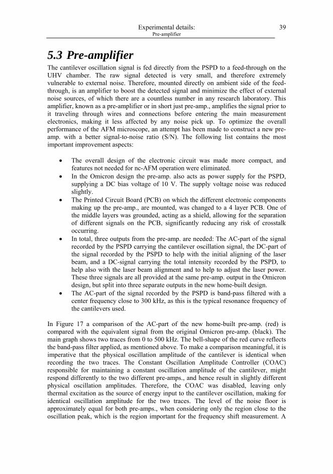
Interdisciplinary Nanoscience Center (iNANO), and Department of Physics and Astronomy, 2007 FACULTY OF SCIENCE UNIVERSITY OF AARHUS Scanning Probe Microscopy Studies of a Metal Oxide Surface PhD Thesis 2007 Scanning Probe Microscopy imaging of single crystal surfaces and nanoscale systems has demonstrated great potential for new advances in science. With the invention and recent development of the Atomic Force Microscope used in the ultra-sensitive non-contact mode, the door has now been opened to detailed studies of the whole range of insulating metal oxide surfaces. As a result, new and challenging issues, especially within the field of heterogeneous catalysis and the effect of metal oxide support materials, may be resolved. The work presented in this thesis addresses two main topics: Firstly, the detailed information available by use of Atomic Force Microscopy is investigated by imaging and analyzing the atomic-scale surface structure of the prototypical metal oxide TiO 2 . Secondly, the use of additional probing techniques, applicable simultaneously during Atomic Force Microscopy imaging, is shown to provide new and valuable insight into the surface properties and the imaging mechanisms in play for the TiO 2 surface. The observations presented here for the TiO 2 surface may be generally applicable, and I believe that the results and methods of analysis may serve as a general reference for future studies of other metal oxide surfaces. Front cover illustration. Non-contact Atomic Force Microscopy image of the TiO 2 (110) surface, resolving individual titanium atoms, hydroxyl groups and oxygen vacancies. The image was published on the front cover of NanoTechnology 17 (14). Scanning Probe Microscopy Studies of a Metal Oxide Surface - a detailed study of the TiO 2 (110) surface PhD Thesis GEORG HERBORG ENEVOLDSEN
Transcript
Interdisciplinary Nanoscience Center (iNANO), and Department of Physics and Astronomy, 2007
FACULTY OF SCIENCE
UNIVERSITY OF AARHUS
Scanning Probe Microscopy Studies of a M
etal Oxide Surface
PhD Thesis 2007
Scanning Probe Microscopy imaging of single crystal surfaces and nanoscale systems has
demonstrated great potential for new advances in science. With the invention and recent development
of the Atomic Force Microscope used in the ultra-sensitive non-contact mode, the door has now
been opened to detailed studies of the whole range of insulating metal oxide surfaces. As a result,
new and challenging issues, especially within the field of heterogeneous catalysis and the effect
of metal oxide support materials, may be resolved. The work presented in this thesis addresses
two main topics: Firstly, the detailed information available by use of Atomic Force Microscopy is
investigated by imaging and analyzing the atomic-scale surface structure of the prototypical metal
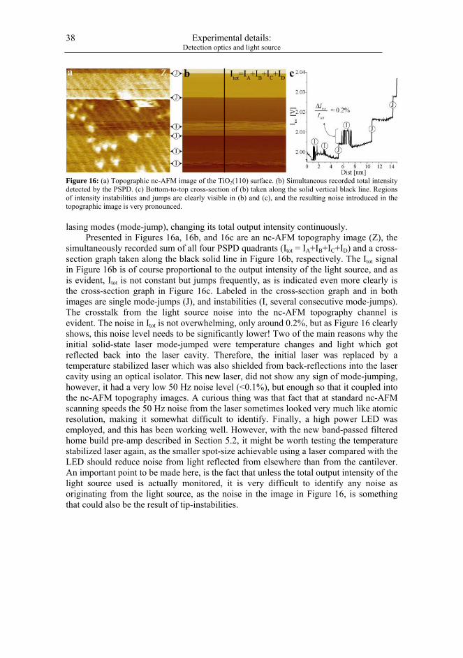
oxide TiO2. Secondly, the use of additional probing techniques, applicable simultaneously during
Atomic Force Microscopy imaging, is shown to provide new and valuable insight into the surface
properties and the imaging mechanisms in play for the TiO2 surface. The observations presented
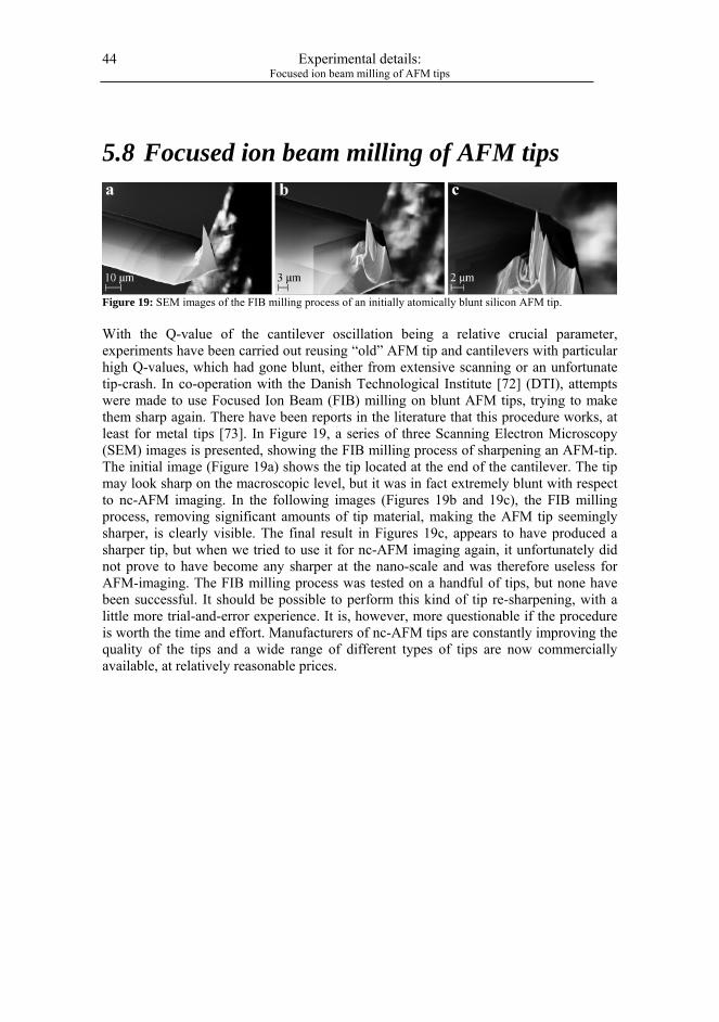
here for the TiO2 surface may be generally applicable, and I believe that the results and methods
of analysis may serve as a general reference for future studies of other metal oxide surfaces.
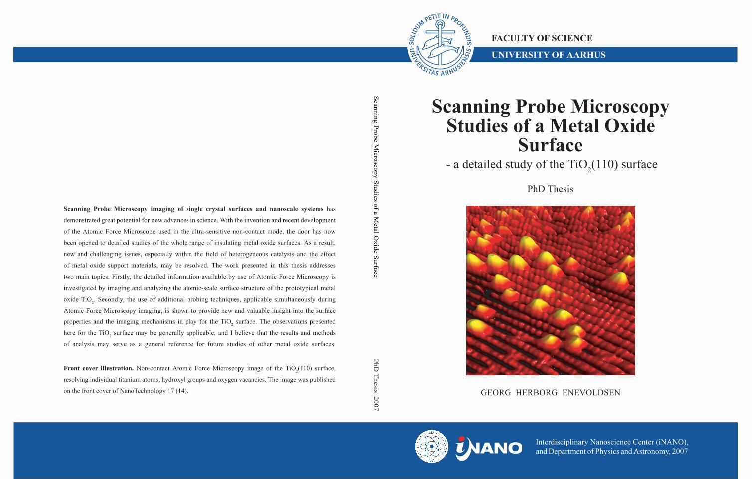
Front cover illustration. Non-contact Atomic Force Microscopy image of the TiO2(110) surface,
resolving individual titanium atoms, hydroxyl groups and oxygen vacancies. The image was published
on the front cover of NanoTechnology 17 (14).
Scanning Probe Microscopy Studies of a Metal Oxide
Surface- a detailed study of the TiO2(110) surface
PhD Thesis
GEORG HERBORG ENEVOLDSEN
Scanning Probe Microscopy Studies of a Metal Oxide
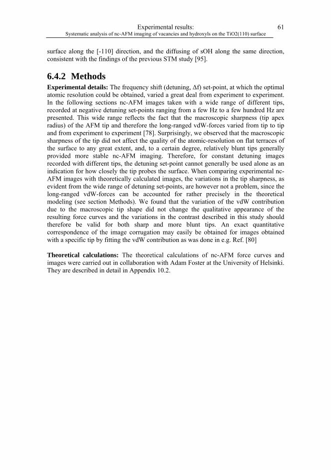
Surface - a detailed study of the TiO2(110) surface
GEORG HERBORG ENEVOLDSEN
Interdisciplinary Nanoscience Center (iNANO) and Department of Physics and Astronomy
University of Aarhus, Denmark
PhD thesis 3rd edition
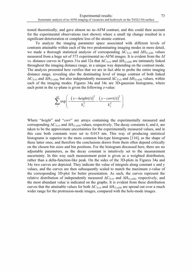
October 2007
ii
Printed by the Reprocenter at the Faculty of Science, University of Aarhus, Denmark, 2007.
This document was typeset in MS Word 2003 by the author
This thesis has been submitted to the Faculty of Science at the University of Aarhus in order to fulfill the requirements for obtaining a PhD degree in physics and nanoscience. The work has been carried out under the supervision of Professor Flemming Besenbacher at the Interdisciplinary Nanoscience Center (iNANO) and the Department of Physics and Astronomy from August 2003 to September 2007.
iii
1 Contents
1 CONTENTS.........................................................................................................III 2 LIST OF PUBLICATIONS .............................................................................. VII 3 PREFACE ............................................................................................................IX
3.1 INTRODUCTION .............................................................................................. IX 3.2 MOTIVATION ..................................................................................................X 3.3 OUTLINE .......................................................................................................XII
4 INTRODUCTION TO ATOMIC FORCE MICROSCOPY ............................. 1 4.1 INTRODUCTION ............................................................................................... 1 4.2 PRINCIPLE OF OPERATION ............................................................................... 2 4.3 FORCES........................................................................................................... 4
4.3.1 Long-range forces ..................................................................................... 4 Van der Waal’s force........................................................................................................ 4 Electrostatic forces ........................................................................................................... 6
4.5 DIFFICULTIES FACED BY AFM...................................................................... 29 4.5.1 Monotonicity and distance dependence................................................... 29 4.5.2 Stability and noise ................................................................................... 29
4.6 AFM SIMULATIONS ...................................................................................... 31 4.6.1 The surface and tip models...................................................................... 31 4.6.2 The simulation......................................................................................... 31
5 EXPERIMENTAL DETAILS ............................................................................ 35 5.1 THE OMICRON UHV SYSTEM AND AFM MICROSCOPE ................................. 35 5.2 DETECTION OPTICS AND LIGHT SOURCE........................................................ 37 5.3 PRE-AMPLIFIER ............................................................................................. 39
5.9.1 Sputter-annealing control ....................................................................... 45 5.9.2 Q-value measurement.............................................................................. 46 5.9.3 Detuning Controller ................................................................................ 47 5.9.4 Image previewing program ..................................................................... 48
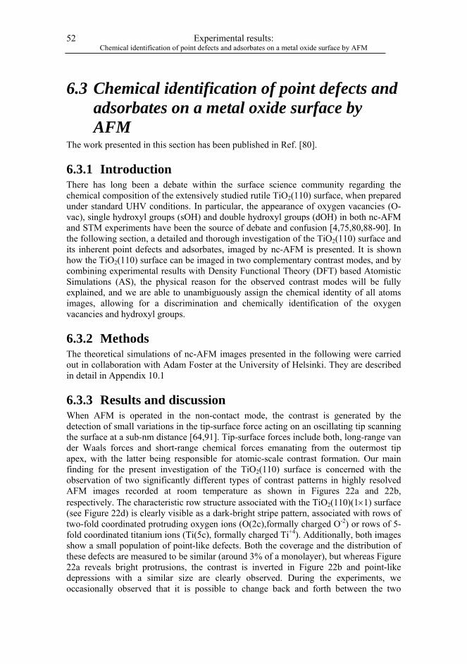
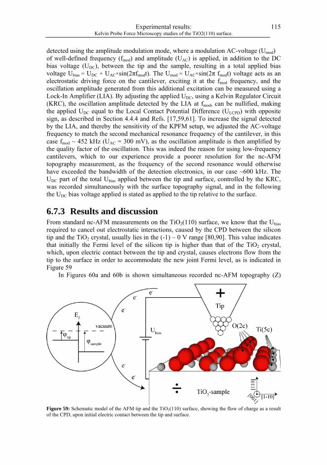
6 EXPERIMENTAL RESULTS ........................................................................... 49 6.1 GENERAL INTRODUCTION............................................................................. 49 6.2 EXPERIMENTAL METHODS ............................................................................ 50 6.3 CHEMICAL IDENTIFICATION OF POINT DEFECTS AND ADSORBATES ON A METAL OXIDE SURFACE BY AFM ............................................................................................ 52
6.4 SYSTEMATIC ANALYSIS OF NC-AFM IMAGING OF VACANCIES AND HYDROXYLS ON THE TIO2(110) SURFACE.................................................................... 60
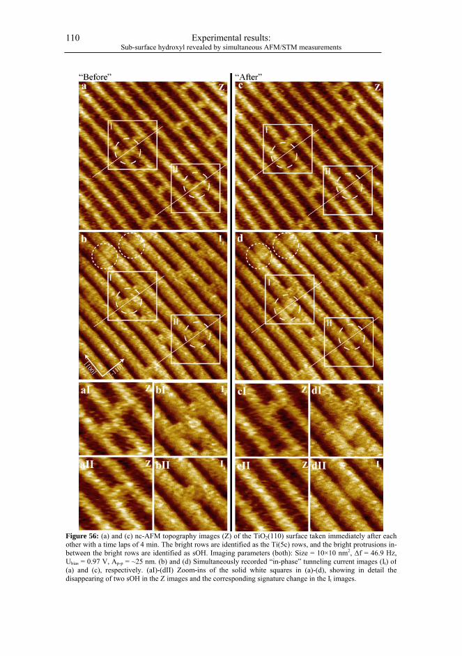
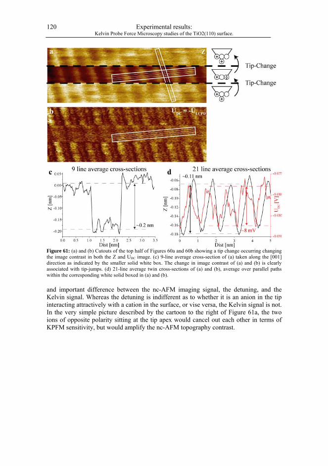
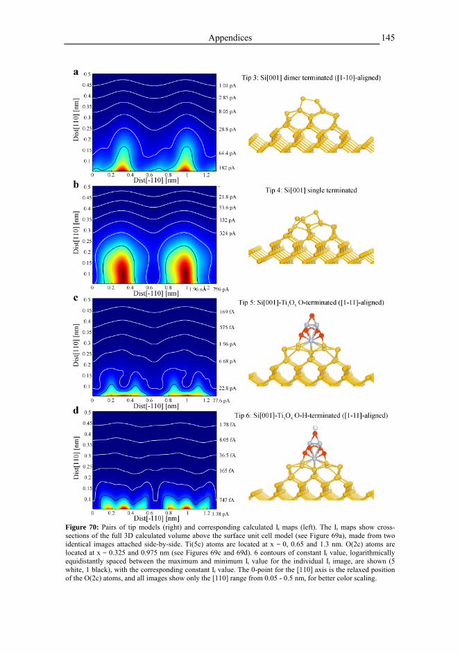
The rutile TiO2(110) surface........................................................................................... 62 Image mode switching.................................................................................................... 63 Negatively terminated tip (protrusion mode).................................................................. 66 Positively terminated tip (hole mode)............................................................................. 69 The covalent tip (neutral mode)...................................................................................... 71 Statistical analysis of different tip terminations and imaging modes.............................. 72 Splitting of dOH and dynamics of sOH groups revisited by nc-AFM............................ 76
6.4.4 Conclusions ............................................................................................. 78 6.5 SIMULTANEOUS AFM/STM STUDIES OF THE HYDROXYLATED TIO2(110) SURFACE ..................................................................................................................... 79
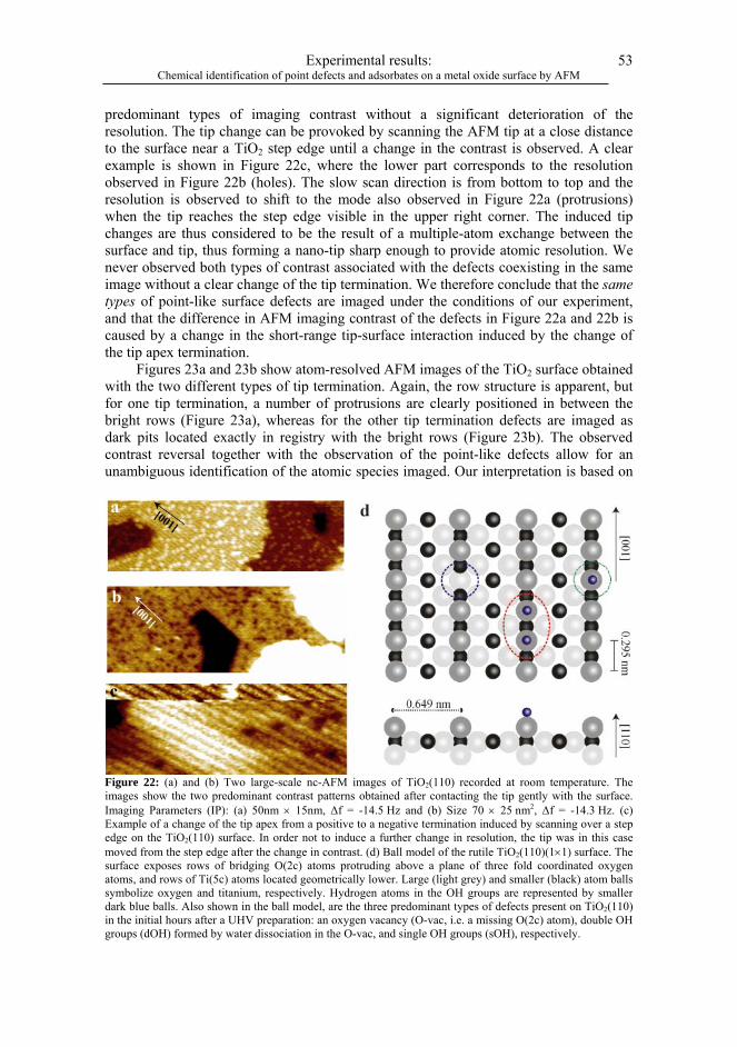
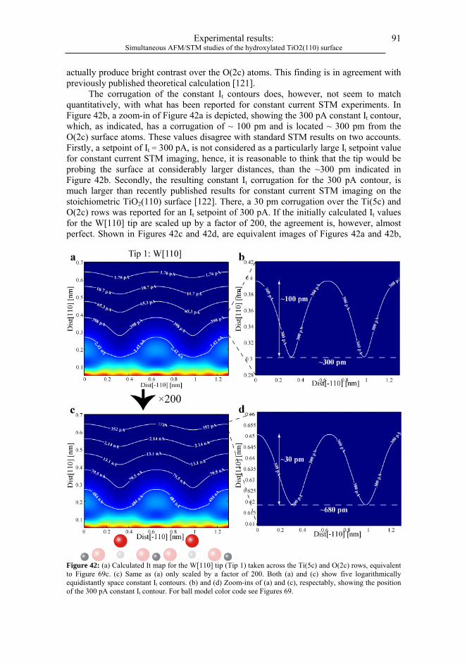
Theoretical calculations.................................................................................................. 90 Identifying the imaging tip structure and chemical composition .................................... 92
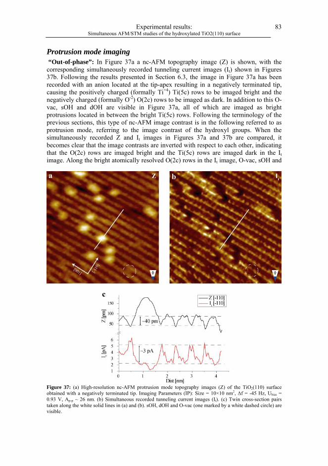
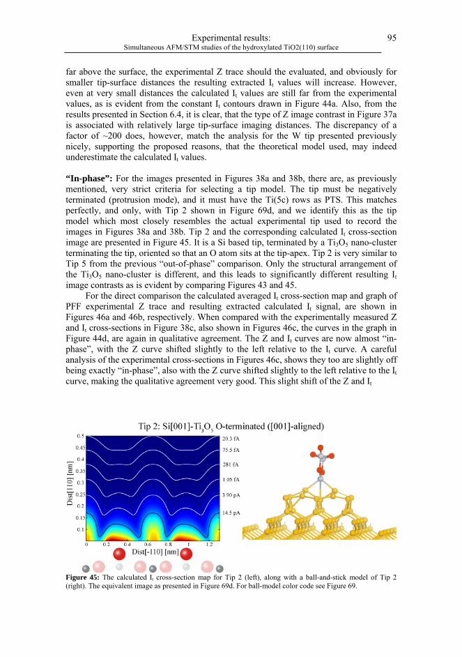
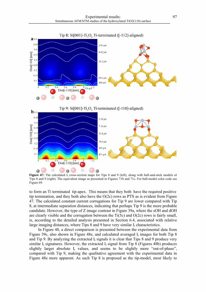
Protrusion mode tip identification. ............................................................................ 93 Hole mode tip identification...................................................................................... 96 Neutral mode tip identification.................................................................................. 99
2 List of publications Publications relevant to this thesis:
I. "Chemical identification of point defects and adsorbates on a metal oxide surface by atomic force microscopy", J.V. Lauritsen, A.S. Foster, G.H. Olesen†, M.C. Christensen, A. Kühnle, S. Helveg, J.R. Rostrup-Nielsen, B.S. Clausen, M. Reichling, and F. Besenbacher, Nanotech., 2006. 17(14): p. 3436-3441.
II. "Noncontact atomic force microscopy imaging of vacancies and hydroxyls on
TiO2(110): Experiments and atomistic simulations", G.H. Enevoldsen, A.S. Foster, M.C. Christensen, J.V. Lauritsen, and F. Besenbacher, Phys. Rev. B, 2007. Accepted.
III. "Simultaneous nc-AFM and tunneling current imaging of a hydroxylated
TiO2(110) surface." G.H. Enevoldsen, H. Pinto, A.S. Foster, J.V. Lauritsen, M.C. Christensen, and F. Besenbacher. In preparation.
IV. "Kelvin probe force microscopy imaging of the atomic scale structure of the
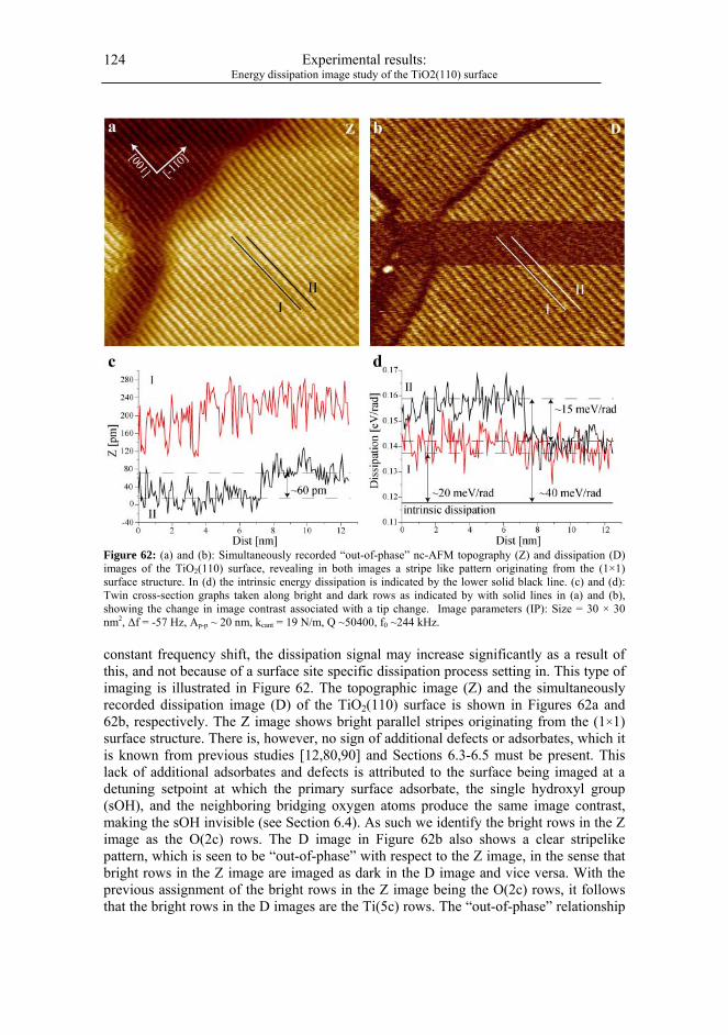
TiO2(110) surface", G.H. Enevoldsen, T. Glatzel, M.C. Christensen, J.V. Lauritsen, and F. Besenbacher. In preparation.
V. "Sub-surface hydroxyl on the TiO2(110) surface revealed by simultaneous
AFM/STM measurements", G.H. Enevoldsen, H. Pinto, B. Hammer, A.S. Foster, M.C. Christensen, J.V. Lauritsen, and F. Besenbacher. In preparation.
Additional publications:
i. "Location and coordination of promoter atoms in Co- and Ni-promoted MoS2-based hydrotreating catalysts", J.V. Lauritsen, J. Kibsgaard, G.H. Olesen†, P.G. Moses, B. Hinnemann, S. Helveg, J.K. Nørskov, B.S. Clausen, H. Topsøe, E. Lægsgaard, and F. Besenbacher, J. Catal., 2007. 249(2): p. 220-233.
ii. "Atomic-scale structure and reactive sites of an aluminum enriched
Al2O3(0001) surface", M.C. Christensen, J.V. Lauritsen, G.H. Enevoldsen, and F. Besenbacher. In preparation.
iii. "The morphology of the polar ZnO(0001) O-terminated surface revealed by nc-
AFM", M.C. Christensen, J.V. Lauritsen, G.H. Enevoldsen, K. Venkataramani, and F. Besenbacher. In preparation.
† As I was recently married I have changed my last name from Olesen to Enevoldsen.
List of publications viii
ix
3 Preface 3.1 Introduction Nanotechnology is the scientific striving towards understanding, characterizing and controlling the physical world around us, all the way down to the atomic scale. The famous words spoken by Richard Feynman in 1959: “There is plenty of room at the bottom”, described the, at that time, elusive world of atoms and molecules, and how there was no physical reasons why these could not be accessed in at controlled way. The later development of scanning probe techniques, with the primary constituents being the Scanning Tunneling Microscope (STM) [1] invented in 1982, and its younger sibling the Atomic Force Microscope (AFM) [2] invented in 1986, have in the past decades confirmed fully the very futuristic ideas presented by Feynman. The invention of these two scanning probe techniques, STM and AFM, constitutes giant leaps in the field of surface science, and the invention of the STM even earned its inventors the Nobel Prize award. The STM and AFM are today surface science analysis tools widely applied in basic research application, continuously exploring the fascinating world of physics and chemistry at the molecular and atomic scale.
The world today is truly becoming a nanotechnology-based society, and detailed atomic-scale understanding of physical processes will become more and more essential for the modern world to function and develop. In the semiconductor industry, the microchip fabrication technology has for several years been pushing the lower limit for the size of the most widely used electronic component, namely the MOS-FET transistor. At present microchip technology is facing a critical situation, where the typical length scales involved are on the order of inter-atomic distances, and the discrete world of quantum physics stands in the way of the continuous employment and development of the fabrication techniques used today. Another area in which nanotechnology is making an impact in the world today is within the field of heterogeneous catalysis. Today more than 50 % of the world’s basic chemicals produced stems from catalytic processes, and catalysis thus constitutes a multibillion Euro business that lies at the very core of modern living. Catalysis is responsible for such diverse areas as producing gigantic amounts of fertilizer enabling the limited agricultural areas of the world to sustain an ever growing population, and it is also applied in the fight against the immense pollution problems in the metropolises of the world, cleaning the exhaust gas from automobiles’ petrol. Even though catalysis is an ancient physical and chemical discipline, it has for many years been governed by a trial-and-error approach, lacking the detailed physical understanding of the individual steps constituting the complete catalytic process.
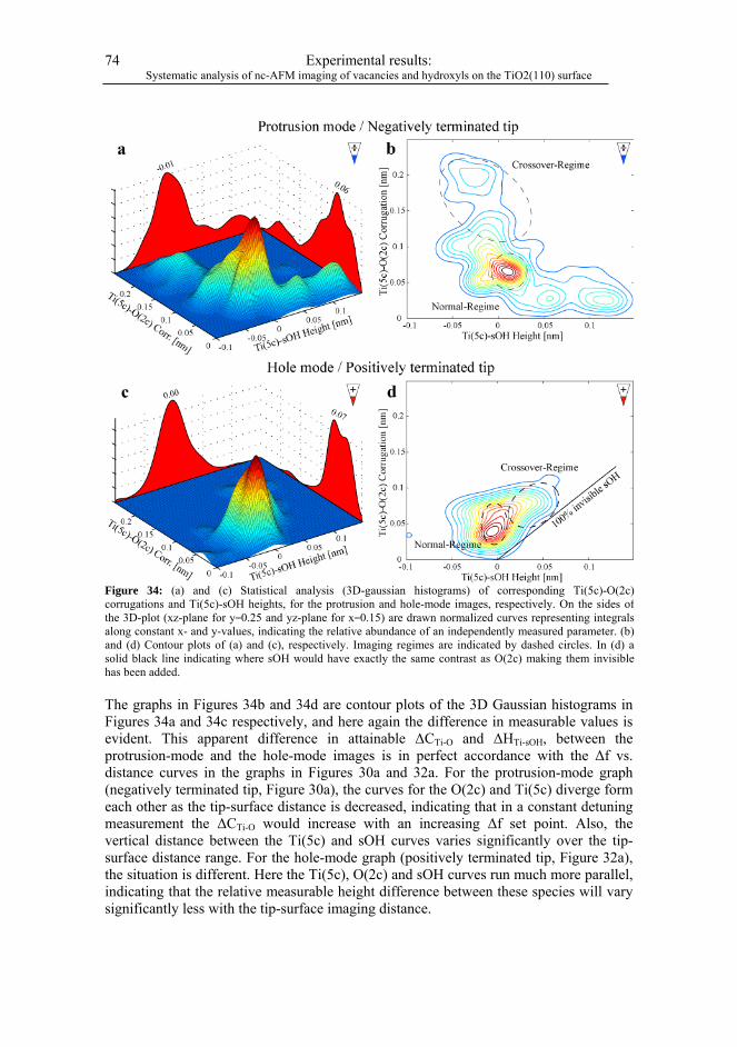
Nanotechnology poses as a scientific discipline capable of solving the problems associated with the continuous development of our modern world, portrayed in the above two technological applications. Nanotechnology is unique in the sense that it combines input from many scientific disciplines, spanning from biology through chemistry and physics to medicine, and combined with the ability to study and characterize the world of atoms and molecules, this approach may be the only way to solve many of the fundamental technological problems facing us today. The abilities of the STM and AFM to image, characterize and manipulate single atoms and molecules in real spaces, have
Preface x
undoubtedly been a major contributor in placing nanotechnology at the very front edge of scientific research.
However, the STM and AFM scanning probe techniques are relatively young, and although they have already shattered many of the paradigms associated with the characterization of the world of single atoms and molecules, there is still plenty of room for further improvement. This improvement is currently both being directed towards producing microscopes with ever increasing image resolution and imaging rate, but also, and perhaps much more interesting and important, towards understanding in detail the images produced by these two techniques. For the AFM, there is in fact a wide range of simultaneous applicable imaging techniques capable of providing many different channels for probing the sample under inspection. This ability provides additional imaging signals available for analysis, and hence a more detailed and complete picture of the sample under inspection can be obtained. From an atomic resolution point of view, major focus is at present being directed towards enabling a direct chemical identification of the individual atoms resolved in high resolution studies. Direct chemical identification has been an inherent limitation for years in scanning probe microscopy, but with the ability to apply several simultaneous probing channels during AFM imaging combined with the rapid progress in image simulations based on advanced theoretical models, this hurdle might be overcome in the years to come.
Metal oxides constitute a range of materials of immense technological interest and importance, stemming from the wide range of properties of this class of materials. The knowledge of metal oxides and in particular their surfaces is, however, sparse compared to that of e.g. metals, and they have eluded surface scientists for years. This fact is largely due to the insulating nature of many of these materials which excludes many of presently available surface science techniques, including STM. In principle AFM is, however, applicable to any surface, and with the continuous development of the AFM, the door is being opened to studying this very interesting class of materials at the atomic level.
3.2 Motivation The materials choice for all experimental results presented in this thesis, was the rutile TiO2(110) surface. The rutile TiO2(110) surface is probably the most studied metal oxide surface [3,4], and there are several reasons for this. TiO2 finds use in a vast range of technological applications. It is used as paint pigments, in gas-sensor technology and for biocompatible implants [3,5]. The use of TiO2 in the field of heterogeneous catalysis, especially using it as support material for catalytically active gold nano-particles, has recently received much attention [6-8]. And finally the photocatalytic properties of TiO2, gives it many interesting applications in the area of photoelectrochemical solar cells [9-11].
Even though the TiO2 metal oxide is a wide band gap semiconductor with a band gap of ~3.0 eV, it reduces easily creating defect states rendering it reasonably conductive. This allows for a wide range of surface science techniques to be applied, especially STM, which in recent years have provided a wealth of detailed information on the (110) surface, resolving it and its prevalent defects and adsorbates in atomic detail [4,12-14]. Additionally, the rutile TiO2(110) surface is the most stable of the low-index rutile surfaces [3], and clean crystal surfaces are prepared easily under UHV conditions using standard surface science techniques. To summarize, the TiO2(110) surface, has become the metal oxide model system, and combining the above mentioned areas of
Preface xi
application and features of the rutile TiO2(110) surface, not only makes it an interesting surface to study for scientific reasons, but it also serves as a very well defined surface template, different from the widely used Si(111)(7×7), for exploring new experimental techniques. Both of these aspects will be addressed in the following sections which discuss the experimental results obtained on the TiO2(110) surface.
As will be described throughout the thesis, many different types of image contrast are attainable in AFM imaging using the non-contact AFM mode of operation [15]. This has led us to examine the types of atomic resolution attainable on the TiO2(110) surface, both in different contrast mode, which will be shown to depend dramatically on the polarity of the AFM tip termination, and also at various tip-surface imaging distances, which will also be shown to affect the resulting image contrast. The ability to probe several different surface properties simultaneously during nc-AFM imaging, is a growing field within the surface science community, as it provides additional surface sensitive channels available for analysis, inspiring us to apply a variety of simultaneous imaging techniques to the extensively studied and relatively well understood TiO2(110) surface.
Results of such studies as described above will not only provide new and valuable insight in the continuous characterization of the TiO2(110) surface, but may also afford new and novel methods of analysis generally applicable to other systems, especially metal oxide surfaces. With the introduction of nc-AFM, the door is opened to analyzing and characterizing the wealth of relatively poorly understood insulating metal oxide surfaces (e.g. ZnO, CeO2, MgO, Al2O3), in atomic detail. Most of these metal oxides already have huge technological importance [3], and any new insight gained in this field is therefore of immense interest and importance.
Preface xii
3.3 Outline This thesis contains a description of the work done and results obtained during my four-year PhD study at the University of Aarhus. The remainder of the thesis is divided into three main sections: Sections 4 – 6, followed by a general summary and outlook.
Section 4: “Introduction to Atomic Force Microscopy”, contains a thorough introduction to the field of Atomic Force Microscopy (AFM), with emphasis on the non-contact AFM mode of operation and the aim of producing atomically resolved images of single crystal surfaces. Also, the various additional scanning probe techniques available simultaneously during nc-AFM imaging are presented. This section is intended as a general reference for newcomers to the AFM field, hopefully providing a solid basis for understanding the basics behind AFM imaging.
Section 5: “Experimental details”, contains an overview of the experimental equipment used for obtaining all experimental data presented in this thesis. This is followed by a description of the practical experimental problems encountered during my PhD studies, along with their solutions. Also presented are some of the programs I have written, to control various processes in the laboratory.
Section 6: “Experimental results”, contains the majority the of experimental results I have been involved in obtaining throughout the course of my PhD study, focusing solely on the work done on the TiO2(110) surface. Some of the results have already been published or submitted for publication (see publication list) whereas other results are in the process of being written up for publication. Presented initially in the section is a general introduction to nc-AFM imaging of single crystal surface.
Finally, a general summary of the experimental results is given, followed by an outlook at the future development of the nc-AFM imaging technique as I see it.
1
4 Introduction to Atomic Force Microscopy
4.1 Introduction The Atomic Force Microscope (AFM) [2] is perhaps the most versatile member of the family of local probe microscopes. It was invented by Binnig and co-workers in 1986, as a spin-off of its older sibling the Scanning Tunneling Microscope (STM) [1]. Both of these scanning probe microscopy techniques utilize a very sharp tip to “feel” rather than “see” the object to be imaged. For single crystals the STM and AFM are capable of resolving surfaces with true atomic resolutions, as was shown in the case of the AFM for the first time in 1995 by Giessibl [16], resolving individual atoms on a single crystal Si(111)(7×7) surface under Ultra High Vacuum (UHV) conditions. Since then the AFM has evolved enormously, and its diversity and versatility enable applications in many different areas of research [17-19].
The possibility of applying AFM imaging under both ambient and liquid environments, has been of great importance for biological applications [19], where samples are often destroyed when removed from their natural environment, e.g. a liquid. For UHV studies of single crystal surfaces, the resolution limit has been pushed to even sub-atomic resolution [20], rendering the AFM a truly cutting-edge performer in ultra high spatial resolution studies. While the STM was the first scanning probe technique capable of obtaining atomic resolution, one of its inherent limitations and major drawbacks, is the requirement for conducting substrates. This limitation is shattered by the AFM, which in principle is applicable to any substrate, including the wealth of insulating materials, in particular metal oxides. Atomic resolution was presented for the first time on a true insulating substrate, namely the Al2O3(0001) surface, by Reichling and co-workers [21], and since then many atomically resolved studies of insulating substrates have followed [18,22].
The following sections describe in detail the basic concepts behind AFM imaging, with main emphasis on imaging single crystal surface with atomic resolution, as well as presenting the different modes of operation available. Also, the above-mentioned wide variety of additional imaging channels available for simultaneous recording are introduced.
Introduction to Atomic Force Microscopy: Principle of operation
2
4.2 Principle of operation
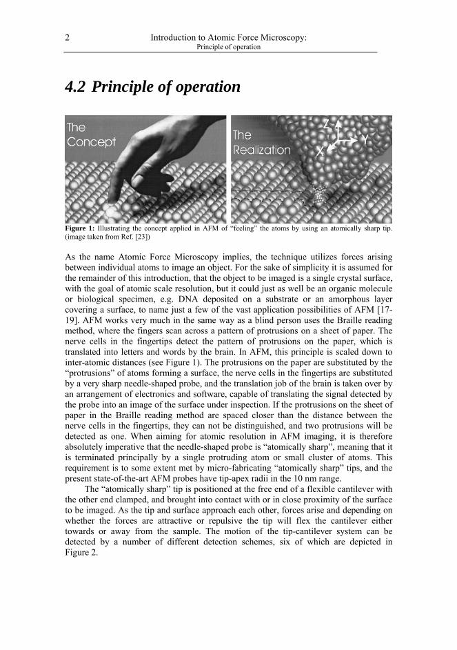
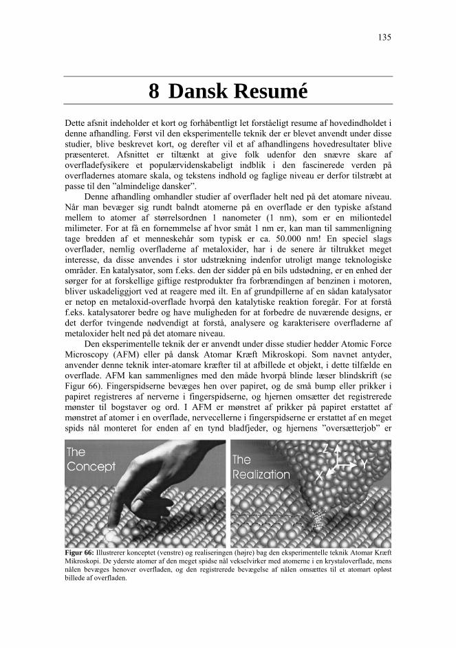
As the name Atomic Force Microscopy implies, the technique utilizes forces arising between individual atoms to image an object. For the sake of simplicity it is assumed for the remainder of this introduction, that the object to be imaged is a single crystal surface, with the goal of atomic scale resolution, but it could just as well be an organic molecule or biological specimen, e.g. DNA deposited on a substrate or an amorphous layer covering a surface, to name just a few of the vast application possibilities of AFM [17-19]. AFM works very much in the same way as a blind person uses the Braille reading method, where the fingers scan across a pattern of protrusions on a sheet of paper. The nerve cells in the fingertips detect the pattern of protrusions on the paper, which is translated into letters and words by the brain. In AFM, this principle is scaled down to inter-atomic distances (see Figure 1). The protrusions on the paper are substituted by the “protrusions” of atoms forming a surface, the nerve cells in the fingertips are substituted by a very sharp needle-shaped probe, and the translation job of the brain is taken over by an arrangement of electronics and software, capable of translating the signal detected by the probe into an image of the surface under inspection. If the protrusions on the sheet of paper in the Braille reading method are spaced closer than the distance between the nerve cells in the fingertips, they can not be distinguished, and two protrusions will be detected as one. When aiming for atomic resolution in AFM imaging, it is therefore absolutely imperative that the needle-shaped probe is “atomically sharp”, meaning that it is terminated principally by a single protruding atom or small cluster of atoms. This requirement is to some extent met by micro-fabricating “atomically sharp” tips, and the present state-of-the-art AFM probes have tip-apex radii in the 10 nm range.
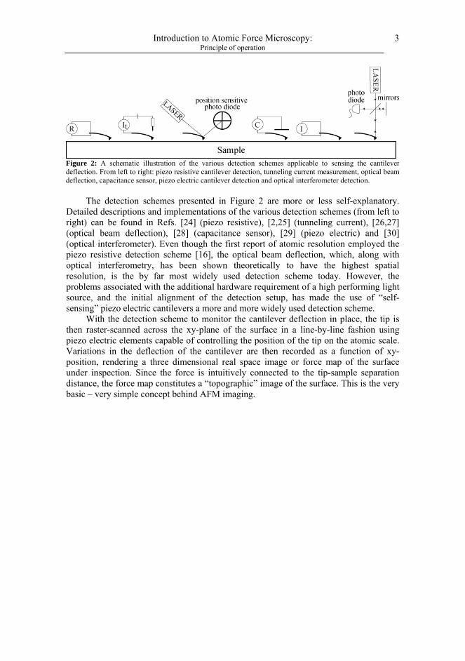
The “atomically sharp” tip is positioned at the free end of a flexible cantilever with the other end clamped, and brought into contact with or in close proximity of the surface to be imaged. As the tip and surface approach each other, forces arise and depending on whether the forces are attractive or repulsive the tip will flex the cantilever either towards or away from the sample. The motion of the tip-cantilever system can be detected by a number of different detection schemes, six of which are depicted in Figure 2.
Figure 1: Illustrating the concept applied in AFM of “feeling” the atoms by using an atomically sharp tip. (image taken from Ref. [23])
Introduction to Atomic Force Microscopy: Principle of operation
3
The detection schemes presented in Figure 2 are more or less self-explanatory. Detailed descriptions and implementations of the various detection schemes (from left to right) can be found in Refs. [24] (piezo resistive), [2,25] (tunneling current), [26,27] (optical beam deflection), [28] (capacitance sensor), [29] (piezo electric) and [30] (optical interferometer). Even though the first report of atomic resolution employed the piezo resistive detection scheme [16], the optical beam deflection, which, along with optical interferometry, has been shown theoretically to have the highest spatial resolution, is the by far most widely used detection scheme today. However, the problems associated with the additional hardware requirement of a high performing light source, and the initial alignment of the detection setup, has made the use of “self-sensing” piezo electric cantilevers a more and more widely used detection scheme.
With the detection scheme to monitor the cantilever deflection in place, the tip is then raster-scanned across the xy-plane of the surface in a line-by-line fashion using piezo electric elements capable of controlling the position of the tip on the atomic scale. Variations in the deflection of the cantilever are then recorded as a function of xy-position, rendering a three dimensional real space image or force map of the surface under inspection. Since the force is intuitively connected to the tip-sample separation distance, the force map constitutes a “topographic” image of the surface. This is the very basic – very simple concept behind AFM imaging.
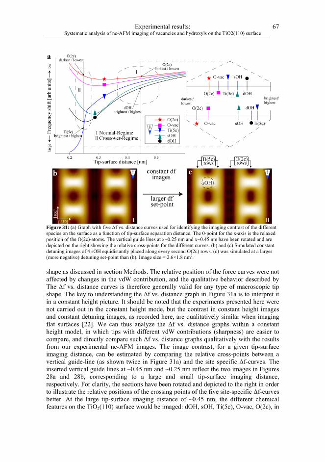
Figure 2: A schematic illustration of the various detection schemes applicable to sensing the cantilever deflection. From left to right: piezo resistive cantilever detection, tunneling current measurement, optical beam deflection, capacitance sensor, piezo electric cantilever detection and optical interferometer detection.
Introduction to Atomic Force Microscopy: Forces
4
4.3 Forces The forces that arise between the tip and the surface, causing the cantilever to deflect, come in a wide variety. Presented here is a selection of these forces, namely those relevant to studies made under Ultra High Vacuum (UHV) conditions. The forces are divided into long-range and short-range forces, depending on their interaction range, since, as will be shown in the following, the interaction range is directly linked to the spatial resolution attainable.
4.3.1 Long-range forces
Van der Waal’s force Long-ranged forces are defined as forces with a range of a few nanometers and more. When forces extend over such a large distance, it implies that several atoms in the tip interact with several atoms in the surface as the tip approaches the surface,. This causes the atomic scale structure of the surface to be smeared out, and atomic resolution is degraded. The van der Waals (vdW) force, which is a dipole-dipole type interaction ever present between individual atoms, belongs to this group. To illustrate this phenomenon, a sketch of two atoms separated by a distance r is shown in Figure 3. The electron cloud surrounding an atom is not completely isotropic. Due to the finite temperature of the atom, thermal energy excites the atom, causing the electron cloud to fluctuate. At a given point in time it may have a distribution as shown for “Atom 1”. This distortion of the electron distribution induces an electric dipole moment pth of “Atom 1”, which in turn sets up a local electric field. This electric field induces dipole moments in surrounding atoms, and the electron cloud of “Atom 2” is therefore also slightly distorted. The interaction energy and hence the force between the two atoms shown in Figure 3 can be estimated relatively easily. The dipole moment of “Atom 1” sets up an electric field given by
( )
2 3
ˆ ˆ3ˆ4 4dip dip
p r r pr pV Er rπε πε
⋅ −⋅= ⇒ =
r rr r (4.1)
Figure 3: A schematic model illustrating the dipole-dipole (van der Walls) interaction of two isolated atoms separated by the distance r.
Introduction to Atomic Force Microscopy: Forces
5
The induced dipole moment “Pind” of “Atom 2” will be proportional to the electric field in Eq.(4.1), and hence the interaction energy “Uint” can be written:
6
6
1ind dip
int ind dip dip dip
int
P E
U P E E Er
CUr
∝
= − ⋅ ∝ − ⋅ ∝ − ⇒
= −
r r
r r r r (4.2)
with C being a proportionality factor depending on several parameters (polarizability of the atoms, permittivity of the separation medium, etc.). Two important things should be noted here. Firstly, the vdW interaction is always attractive for UHV, as C is here always positive. However, the vdW interaction can be made repulsive by a careful choice of separation medium [31]. Secondly, the interaction energy seems to actually fall off relatively quickly with an 61 r dependence. However, the vdW force between the tip and the surface becomes a cumulative effect, as dipoles are continuously induced in atoms throughout the tip and the surface, and to calculate the total vdW force a summation of all dipole-dipole interacting pairs of atoms must be made. Due to the long-ranged nature and resulting cumulative effect, the number of interacting atoms is for all practical purposes “infinite”, making a discrete summation over all interacting pairs of atoms impossible. However, the discrete summation can be replaced by an integration, simplifying the calculation, providing a few assumptions can be made: The atomic structure of the tip and the surface is approximated by a continuous media of constant density, and the material properties are expected to be constant over the integration volume. With these assumptions the total vdW force between the tip and the surface can be written:
2 1
2 1
1 2 1 26
1 26 21 1
vdWV V
vdWV V
CF dV dVr
F H dV dVr
ρ ρ
π
⎛ ⎞= −∇ − ⇔⎜ ⎟⎝ ⎠
⎛ ⎞= −∇ −⎜ ⎟⎝ ⎠
∫∫
∫∫ (4.3)
where V1 and V2 are the integration volumes and ρ1 and ρ2 are the atomic number densities of the tip and the surface, respectively. To simplify even further a material dependent integration constant, known as the Hamaker constant is introduced in Eq. (4.3), H = π2Cρ1ρ2 which has been calculated and listed for a wide range of materials [32]. This leaves a purely geometric integral which has been carried out and tabulated for a number of different geometries [33]. Below the total vdW force between a semi infinite crystal and a pyramidal shaped tip with opening angle θ is written:
( )22 tan
3vdWH
Frθ
π= (4.4)
where r is the distance between the tip apex and the surface. Eq. (4.4) shows that the
Introduction to Atomic Force Microscopy: Forces
6
initial 71 r distance dependence of the vdW force, has been changed by the integration to an 11 r dependence, and this is exactly the reason for the long-range nature of the vdW force. Long-ranged interactions are undesirable when aiming for atomic resolution, but since the vdW force is an intrinsic property of matter, it is ever present. The effect can, however, be screened, reducing the vdW force considerably by immersing the tip and surface in a liquid, e.g. water [33,34]. For UHV application, the vdW forces can also be reduced, by using sharp tips, as this reduces the effective integration volume in Eq. (4.3).
Electrostatic forces Another long-ranged force is the electrostatic force. Formally the electrostatic force between two uniformly charged objects falls off with an 2
1r distance dependence,
justifying the long-range classification. Charging in AFM can arise from many different sources. For insulating single crystal surface imaging under UHV conditions, the surface cleaning process, either by ion bombardment or by cleaving, can leave the surface charged. This charging can, however, often be removed by heating up the crystal, making the trapped charges mobile enough to diffuse away.
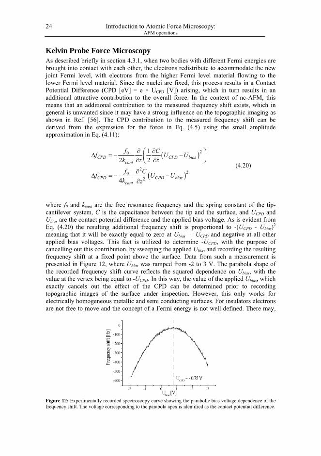
There is, however, another type of electrostatic interaction with a more complex origin. When two materials with different work functions are brought into electric contact (e.g. the AFM tip and the surface to be scanned), the electrons will redistribute in order to accommodate the new joint Fermi level. Since the atomic nuclei are fixed, a charging of the materials occurs, as electrons of the smaller work function material flow to the higher work function material. This charging sets up a potential difference between the two connected materials, known as the Contact Potential Difference (CPD [eV] = e × UCPD [V]), which in a simple model is equal to the initial Fermi level energy difference (divided by the electron charge). In the context of AFM, this means that there exists an intrinsic potential difference between the AFM tip and the surface under inspection, which will result in an additional long-ranged attractive force. The force between two charged objects, in this context the tip and the sample, between which there exists a potential difference, Utot, is given by [35]:
( )221 12 2tot CPD bias
C CF U U Uz z
∂ ∂= = +
∂ ∂ (4.5)
where C is the capacitance between the tip and the sample. In the last step in Eq. (4.5), the total potential difference, Utot, has been explicitly written as the sum of the intrinsic contribution UCPD, and an externally applied bias voltage Ubias. This makes it evident that the UCPD contribution to the total force can be cancelled out, by applying a bias voltage equal in magnitude to the UCPD but with opposite sign, between the tip and the surface. The distance dependence and sign of the force in Eq. (4.5), is hidden in the capacitance gradient. The capacitance between two objects always decreases with distance, making
Cz
∂∂ intrinsically negative and the force in Eq. (4.5) attractive. If the tip and surface are
approximated by a parallel plate capacitor, the capacitance gradient, and hence the force in Eq. (4.5) will behave as 21 r− . This topic and its applications in the field of Kelvin probe force microscopy, will be discussed further in section 4.4.4.
Introduction to Atomic Force Microscopy: Forces
7
4.3.2 Short-range forces Short-range forces are defined as forces with a range of less than 1 nm. These originate from the formation and breaking of chemical bonds between atoms in the tip and the surface, and it is the confinedness of the electronic orbitals that limits the interaction range, effectively to include only the outermost tip-apex atom, and the nearest surface atom. The chemical forces can be both attractive and repulsive in nature, depending on the distance between the tip and the surface, and the chemical nature of the interacting atoms. In a simple picture chemical forces can be described as follows: When two atoms are far from each other, the electronic orbitals do not “feel” each other (the overlap of the orbitals is vanishing) and no chemical force acts between the atoms. As the atoms are moved closer together the valence orbitals start to overlap, forming molecular bonding and anti-bonding orbitals, and energy is gained by filling valence electrons into the molecular bonding orbitals. This results in an attractive force driving the atoms closer together. At some point the overlap of valence orbitals is optimal, pushing the energy level of the bonding molecular orbital to its lowest possible energy, and the attractive force vanishes. The separation distance where this occurs is also known as the chemical bond length. An attempt to push the atoms even closer together results in a repulsive force between the atoms, originating from the Pauli Exclusion Principle and ultimately ion-core repulsion between the nuclei. The precise analytical behavior of the interaction force, or equivalently interaction energy, is difficult to predict, as it of course depends intimately on the chemical nature of the two interacting atoms. Several approximations have been proposed to mimic the distance dependence of chemical interaction as described above, and one‡ of the most well-known is the Morse Potential written below in Eq. (4.6)
( ) ( )( )( ) ( )( )
2
22
2e e
e e
r rmorse bond
r rmorse bond
V E
F E
κ σ κ σ
κ σ κ σκ
− − − −
− − − −
= − +
= − − (4.6)
where Ebond, σ and κ, are the chemical bonding energy, bond length and decay constant, describing how fast the interaction energy (or force) changes with distance, respectively. The first exponential term in the parenthesis in Eq. (4.6) governs the energy and force at r >> σ, causing the initial attractive behavior between the atoms. When r = σ the interaction energy reaches a minimum and the force vanishes. At r << σ the second exponential term takes over, and the interaction energy shoots up resulting in a repulsive force. The exponential description of the chemical forces in the Morse Potential justifies the short-ranged classification.
Introduction to Atomic Force Microscopy: AFM operations
8
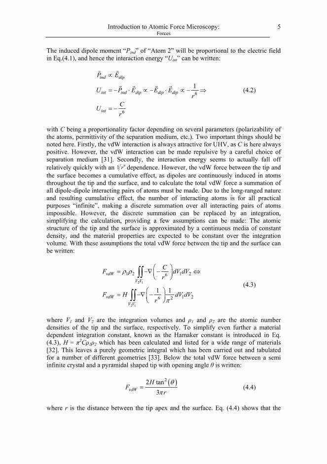
4.4 AFM operations In the previous section, the various forces interacting between the AFM tip and a surface were listed, and in Figure 4 a total force curve is presented, which shows both the long-ranged vdW force, the short-ranged chemical force (Morse type) and the resulting total force. The graph is divided into five regions:
1) At large separation distances the total force is completely dominated by the vdW interaction.
2) As the separation distance decreases, the chemical forces start to increase in magnitude, adding to the overall attractive force.
3) The chemical forces start to dominate the total force and this is the point of largest positive total force gradient.
4) The point of maximum attractive force. 5) At very small separation distances the total force becomes strongly repulsive.
Figure 4: The graph shows the short-ranged (chemical) and long-ranged (vdW) contributions to the total force (the sum of the two) acting between the AFM tip and the surface.
Introduction to Atomic Force Microscopy: AFM operations
9
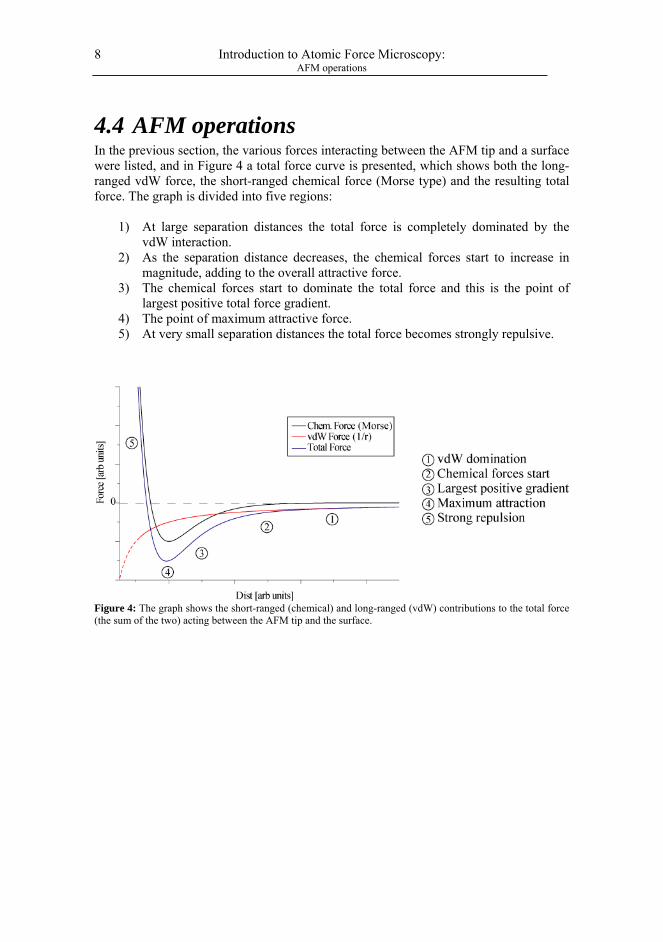
4.4.1 Contact AFM In contact AFM the tip and surface are, as the name implies, brought into contact with each other. However, to be “in contact” is not a well defined state at the nano-scale. On the macroscopic scale, to be “in contact” is associated with a strong repulsive interaction between the two objects, like at the point of impact between two colliding balls in a game of billiards, or a book lying motionless on a table, with the normal and gravitational force cancelling each other. At the nano-scale things are slightly more complicated, since both attraction and repulsion occur at very short separation distances (see Figure 4). In contact AFM the AFM tip is brought into contact with the surface, meaning the repulsive regime labeled “5” in Figure 4. In Figure 5 a sketch of the outermost part of the tip-cantilever system, with the atomic structure of the tip-apex is indicated (not to scale). Below the tip the three top-most atomic layers of a crystal are shown, with one atom missing in the top-most layer, creating an atomic defect. As the tip is scanned across the surface, the repulsive interaction between the tip-apex atom and the surface atoms will cause the cantilever to flex back and forth, tracing out the geometric contour of the surface, as indicated by the “trace-line” in Figure 5. This motion can be detected by any one of the detections schemes outline in section 4.2. The left picture in Figure 5 shows the ideal case, where the AFM tip is terminated by a single atom. The tip traces the atomic structure perfectly, resolving even the atomic defect, providing genuine atomic resolution of the surface imaged. However, the repulsive force between the tip and surface needs to be of a certain magnitude for it to result in a detectable deflection of the cantilever, a value limited by the softness or spring constant (kcant) of the cantilever through ∆z = kcant × Ftip-surf. When the total force is sufficiently repulsive to generate a measurable deflection of the cantilever, it will be composed of both short-ranged repulsive (chemical) and longer-ranged attractive (vdW) contributions, and the inter-atomic chemical repulsive force may be an order of magnitude larger than the overall net repulsive force. This means that with a lower detection limit for the force lying in the 0.1 nN range, the short-ranged repulsive force between the tip and surface atoms is in the same range or greater than the inter-atomic force between the atoms within the tip and the surface themselves. It was realized relatively early [36], that forces of such magnitude existing between individual atoms lead to a high risk of irreversible damage occurring either on the surface, ruining the surface structure, or at the tip destroying the atomic sharpness making it blunt. A blunt tip will have more individual atoms interacting between tip and surface, and the repulsive force needed to generate a sufficient signal is shared between all interacting atoms, reducing the risk of damage. A
Figure 5: A schematic model of contact AFM imaging. The IDEAL tip maps perfectly the atomic structure of the surface ball model. The trace of the “REAL” tip, illustrates the periodic motion of the tip mimicking atomic resolution, however failing to detect the point defect in the surface ball model.
Introduction to Atomic Force Microscopy: AFM operations
10
more realistic blunt tip is depicted to the right in Figure 5, where the tip-apex is composed of three atoms. The indicated tip trace across the surface still seems to map out the atomic structure of the surface, providing an apparent atomically resolved image of the surface, but this in not the case! The fact that imaging is done with a blunt three-atom tip, makes the atomic defect invisible, and the atomic resolution indicated by the tip trace reflects only the surface periodicity and not its genuine atomic structure. The large repulsive interaction between the tip-apex and surface atoms, required to make the overall interaction repulsive, can be reduced by pulling slightly on the cantilever, sharing the repulsive force between the short-ranged atomic interaction and the spring action of the cantilever. In this way the tip can probe the surface further away, even in the attractive regime labeled “3” in Figure 4, reducing the risk of irreversible damage occurring to the tip and/or surface.
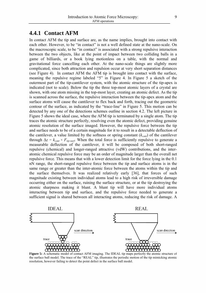
4.4.2 Non-contact AFM Non-contact AFM (nc-AFM) operates at larger separation distances compared to contact AFM. Nc-AFM is a dynamic scanning process, where the tip-cantilever system no longer scans the surface in a static / passive fashion as in the case of contact AFM. Instead the cantilever is made to oscillate in close proximity of the surface as shown in Figure 6. At the lower turning point of the oscillation cycle the short-ranged chemical forces, and the long-ranged vdW forces interact between the tip and the surface, but, contrary to contact AFM, the tip probes the surface at a “safe distance”, meaning that the minimum distance between the tip and the surface is large enough to avoid irreversible damage. The sinusoidal oscillation of the cantilever is detected, and from this the amplitude and frequency (and phase) of the oscillation can be recorded. The imaging mechanism of nc-AFM can be understood from a classical mechanics analysis of the motion of the cantilever (z), which, using Newton’s 2nd law, can be written as: ( )coseff dr dr cant eff tsm z F t k z m z Fω γ= − − +&& & (4.7) where meff, Fdr, ωdr, kcant and γ are the effective mass of the tip-cantilever system, the magnitude and frequency of the excitation force driving the oscillation, the cantilever spring constant and the oscillation damping, respectively. The meff and kcant terms in Eq. (4.7), enabling a point-mass-on-a-spring type description, can be linked to the material properties of the cantilever through the following equations [37]:
Figure 6: Schematic model of the principle behind non-contact AFM imaging. The zoom-in illustrates the long-ranged vdW interaction of several tip and surface atoms, whereas the short-ranged chemical interaction principally only exists between the tip apex atom and the surface atom directly below.
Introduction to Atomic Force Microscopy: AFM operations
11
3
3 ; 0.244Y
cant eff cantE wt
k m mL
= ≈ × (4.8)
where EY, w, t, L and mcant, are Young’s modulus, width, thickness, length and total mass, of the (rectangular / beam) cantilever, respectively. For the description presented here the additional mass of the AFM tip has been neglected, which is generally a good approximation. For a detailed description of cantilever dynamics see Ref. [38]. The last term on the right side, is a force term including all forces interacting between the tip and the surface, the total tip-surface force. Disregarding the total tip-surface force term (Fts), Eq. (4.7) describes a forced damped harmonic oscillator with textbook steady-state solutions for the tip motion [39]:
( )2
22 2 00
002 2
0
( ) cos( )1
arctan ; ;
dr
dr
effdr
dr
dr cant
effdr
z t A tF
Am
Q
kQ
m
ω ϕ
ω ωω ω
γω ωϕ ω
γω ω
= +
=⎛ ⎞
− + ⎜ ⎟⎝ ⎠
⎛ ⎞= = =⎜ ⎟⎜ ⎟−⎝ ⎠
(4.9)
where A, φ, ω0 and Q are the oscillation amplitude and phase, the mechanical resonance frequency of the freely oscillating tip-cantilever system and the quality factor (Q-value) of the oscillation§, respectively. Including the Fts term in Eq. (4.7) complicates things considerably, since an exact expression for Fts requires a detailed knowledge of all interacting atoms, and still then it may prove extremely difficult to model exactly. To solve the equation of motion of the tip-cantilever system including Fts, thus requires a simplified analytical approximation to be made for the tip-surface force.
Small amplitude approximation In the small amplitude approximation, the oscillation of the tip-cantilever system is considered to be small enough that the tip-surface force term can be approximated by a first order Taylor expansion.
( )
( )
0
cos
cos ( )ts
tseff dr dr cant eff
z z
k
eff dr dr cant ts eff
dFm z F t k z m z z
dz
m z F t k k z m z
ω γ
ω γ
=
= − − +
= − − −
&& &
14243c
&& &
(4.10)
In this approximation the equation of motion is particularly easy to solve since the first order derivative of the tip-surface force, kts, can be included as an additional spring constant term as shown in the last step in Eq. (4.10). This means that the equation of § The quality factor Q is defined as
energy stored in the oscillatorQenergy dissipated per radian
=
Introduction to Atomic Force Microscopy: AFM operations
12
motion is exactly the same as for the forced damped harmonic oscillator in Eq. (4.9), except for one very important detail:
The resonance frequency changes. This is the all important key point in nc-AFM imaging, which, as will be show later, is also valid beyond the small amplitude approximation. The new expression for the resonance frequency of the tip-cantilever system becomes:
00
00
2
; 2
cant ts tsres
eff cant
tsres
cant
k k km k
f kf f f f
k
ωω ω
−= = − ⇒
= + ∆ ∆ = −
(4.11)
where a shift from the angular frequency ω, to the “normal” measure of frequency f has been made, with the standard relation 2 fω π= , since this is the unit generally used in nc-AFM. From Eq. (4.11) it is clear that the resonance frequency shifts down if the tip-surface force gradient (kts) is positive and vice versa. Since the system is now sensitive to the force gradient, and not the absolute force, it is instructive to plot the derivative of the total force, as shown in Figure 7, along with the regimes of positive and negative frequency shift. In nc-AFM the surface is usually probed in the attractive regime with a negative frequency shift, indicating that the tip-surface imaging distance is
Figure 7: Graph showing both the total force between the tip and the surface, and the resulting force gradient. The regions available for probing with a positive or negative resulting frequency shift. The lack of monotonicity excludes the unshaded region (see Section 4.5.1).
Introduction to Atomic Force Microscopy: AFM operations
13
significantly larger compared with contact AFM, greatly reducing the risk of irreversible damage occurring. Since the force gradient depends on the tip-surface separation distance, so does the resulting frequency shift, and it can hence be used to generate a topographic image of the surface under inspection. In the following sections, two different schemes for detecting this frequency shift will be described.
Large amplitude approximations Even though the small amplitude approximation presented in the previous section gives a fully valid intuitive introduction to and explanation of the mechanisms in play changing the resonance frequency in nc-AFM imaging, relating the frequency shift to the tip-surface force gradient and ultimately to a measure for the tip-surface distance, it is an idealized scenario. Under real experimental imaging conditions, the cantilever oscillation amplitude is often several nanometers or even tens of nanometers, which is orders of magnitude too much for the first order Taylor expansion of the tip-surface force to suffice. In this case more advanced mathematical tools must be employed. This section gives a short overview.
In the large amplitude approximation, that is, for oscillation amplitude much larger than the minimum separation distance between the tip and the surface (A >> d), it can be shown, using the Hamiltonian-Jacobi formalism [40], that instead of the simple expression for the frequency shift in Eq. (4.11) a more general expression can be deduced**:
02
22 ts time
cant
ff F z
k A∆ = − (4.12)
The deriviation of Eq. (4.12) relies on a first order perturbation theory approach, and as such the tip-surface interaction potential must be small compared with the potential energy of the oscillating cantilever. This is, however, almost always fulfilled, since the interaction energy typically lies in the eV range, whereas the energy of the cantilever oscillation is several keV. The simple Eq. (4.11) relating the frequency shift proportionally to the tip-surface force gradient has been replaced by an expression including the time average over an oscillation cycle of the force-position product. At first glace it looks as if the frequency shift now depends on the absolute force and not the force gradient, but carrying out the time average in Eq. (4.12), integrating by parts and rewriting the resulting expression, reveals that this is not the case. The result is shown below in Eq. (4.13)
( )2 2 20
2
2 ( )2
d Ats
dcantweight function
ff k z A z d A dz
k A π
+−∆ = − − −∫
14444244443 (4.13)
where A and d are the oscillation amplitude and minimum tip-surface distance, respectively. From Eq. (4.13) it is evident that the frequency shift is indeed still dependent on the tip-surface force gradient kts, however, now in a slightly more complicated form. The expression in Eq. (4.13) can be understood as a weighted average ** In this expression z = 0 is the equilibrium position for the cantilever
Introduction to Atomic Force Microscopy: AFM operations
14
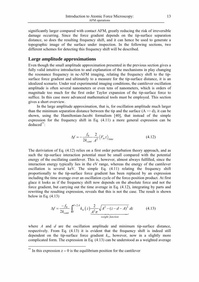
of the force gradient over half an oscillation cycle, with the weight function being a semi-circle of radius A, centered at z = d+A and scaled to a constant (unity) area. To illustrate how the expression in Eq. (4.13) translates into a frequency shift, the total force gradient along with three different weight functions have been plotted in Figure 8. The three different weight functions correspond to three different oscillation amplitudes of 0.1, 0.4 and 0.8 in arbitrary units, respectively. The outline of the semi-transparent shaded regions indicates the convolution of the different weight functions and the total tip-surface force gradient (kts), and the area of these shaded regions thus represents the integral in Eq. (4.13), making them proportional to the resulting frequency shift. It is clear from the graph in Figure 8 that the use of small oscillation amplitudes is desirable for two reasons:
Figure 8: The graph illustrates the resulting frequency shifts in the large amplitude limit at three different amplitudes. The black curve represents the total force gradient between the tip and the surface. The blue, red and green curves represent three different weight functions, and the blue, red and green-shaded semi-transparent areas represent the integral of Eq. (4.13), to which the frequency shift is proportional.
Introduction to Atomic Force Microscopy: AFM operations
15
1) When aiming for high or even atomic resolution, it is desirable to be sensitive
to the short-ranged (chemical) forces, and not the long-ranged (e.g vdW forces). This is clearly the case when the oscillation is small, since the tip then “spends more time” in the presence of the short-ranged chemical forces at small tip-surface distances.
2) As indicated in Figure 8, the area of the semi-transparent regions, which is
proportional to the frequency shift, increases with a decreasing oscillation amplitude. This is due to the fact that the weight function for small oscillation amplitudes, amplifies the relative large kts contributions from the short-ranged chemical forces at small tip-surface distances, resulting in a larger frequency shift.
For the situation depicted in Figure 8 reducing the amplitude by a factor of eight, from 0.8 to 0.1 not only makes the AFM more sensitive to the short-ranged forces, but it also increases the resulting frequency shift by almost a factor of 5, improving the signal-to-noise ration (S/N) even though the minimum distance at which the tip probes the surface is the same. It should be noted that the A = 0.1 weight function in Figure 8 might not be valid in the large amplitude approximation (A >> d), but the analysis presented here shows the general trend intuitively.
A compact expression for the frequency shift can be derived [40], shown in Eq. (4.14), if the tip-surface interaction force can be described by either an inverse power law or by an exponential dependence, which is generally a good description since both the vdW and Morse forces fall within these categories.
( ) ( )
( ) ( )
00 3
2
32
00
, , ,
, , ,
cant
cant
cantcant
ff f A k d d
k A
k Ad f f A k d
f
γ
γ
∆ = ⇔
= ∆
(4.14)
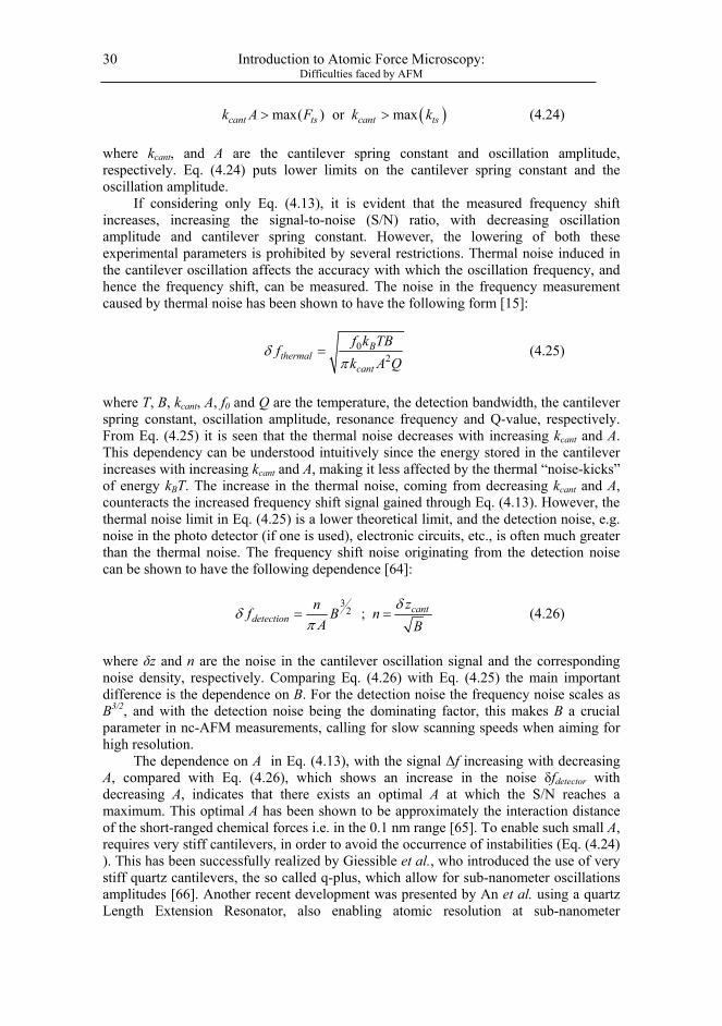
Eq. (4.14) shows how the complicated dependence of the frequency shift on a wide range of parameters can be reduced to a “normalized frequency shift”, γ, which is only dependent on a single parameter, namely the minimum tip-surface distance, d. The “normalized frequency shift” γ, can thus be used to decouple the external experimental imaging parameters kcant, A and f0, from the measured frequency shift, allowing for a comparison between experiments conducted with different kcant, A and f0.
It is evident from Eqs. (4.11) and (4.14) that larger resonance frequencies increase the resulting frequency shift, and as such high resonance frequency cantilevers are desirable. Also evident from Eqs. (4.11) and (4.14) is the fact that a smaller kcant, and in the case of Eq. (4.14) also a smaller A, will additionally act as to increase the resulting ∆f, improving the S/N of the nc-AFM detection. However, the decrease of kcant and A, does not come without a price, as will be illustrated later (see Section 4.5.2).
Introduction to Atomic Force Microscopy: AFM operations
16
Amplitude Modulation AFM In the previous sections it was explained in detail how the mechanical resonance frequency of an oscillating tip-cantilever in close proximity to a surface is changed. This section describes how this phenomenon can be exploited to image a surface, by a technique called Amplitude Modulation AFM (AM-AFM) also known as slope detection, which was introduced by Martin et al. in 1987 [41]. In AM-AFM the resonance phenomenon of the oscillation cantilever is used to measure the shift in resonance frequency (∆f), caused by the tip-surface force gradient, through Eqs. (4.11) or (4.13), which in turn can be used to generate a topographic 3D real-space image of the surface. The resonance phenomenon on the tip-cantilever system is evident from the expression of the oscillation amplitude as a function of driving frequency in Eq. (4.9). When the system is driven exactly at its resonance frequency, the resulting oscillation amplitude reaches a maximum. If the driving frequency is slightly off resonance, either higher or lower, the oscillation amplitude will decrease. The detection scheme, relating the resulting measurable oscillation amplitude to the frequency shift, is depicted in Figure 9. The tip-surface force and force gradient as a function of distance are shown in Figure 9a. At the point labeled (1) the tip is so far from the surface that the force gradient is effectively zero and the resonance frequency of the tip-cantilever system is equal to the free resonance frequency without the presence of the surface. In Figure 9b the resonance curve for the cantilever oscillation amplitude corresponding to this situation is shown in red. In AM-AFM the driving frequency is set to be slightly off (typically higher than) the free resonance frequency, resulting in a reduced oscillation amplitude, labeled “free osc. ampl.”. As the oscillating tip is brought closer to the surface, the situation is labeled (2) in Figure 9a, the long and short-ranged forces cause a negative shift of the resonance frequency of the cantilever. The negative shift in resonance frequency, shifts the entire resonance curve of the tip-cantilever system, shown in blue in Figure 9b, so that the “new” resonance frequency is even further away from the driving frequency, resulting in a decrease in oscillation amplitude. The change in oscillation amplitude can easily be measured, and as the tip scans across the surface, the surface geometry, step edges, adsorbates, etc. will affect the tip-surface distance, shifting the resonance frequency, resulting in an increase or decrease in oscillation amplitude. In this way the measured change in oscillation amplitude can be used as a measure for the tip surface separation distance and used to generate a topographic 3D real-space image of
Figure 9: Graphs illustrating the detection principle of AM-AFM. (a) Tip-surface force and force gradient. (b) Resonance curve of the freely oscillating (red) and resonance frequency shifted (blue) cantilever, corresponding to distances labeled (1) and (2) in (a). The decrease in oscillation amplitude (∆A), resulting from the tip-surface force gradient induced resonance frequency shift (∆f), is indicated.
Introduction to Atomic Force Microscopy: AFM operations
17
the surface. To avoid the effect of an increase or decrease in oscillation amplitude on the absolute tip-surface distance, a constant amplitude feedback loop is applied, adjusting the driving amplitude of the cantilever actuator, in order to maintain a constant amplitude. In this respect the imaging signal becomes the driving amplitude of the cantilever actuator, since the oscillation amplitude is now kept constant, but otherwise the detection principle is equivalent to the above description.
The previously mentioned Q-value can be estimated from the full-width-half-maximum (FWHM) value of the resonance curve (in the low damping limit) by the formula shown in the graph. It is clear that the Q-value is linked to the sharpness of the resonance peak, with the Q-value increasing as the resonance peak narrows. This fact makes it evident that the sensitivity of AM-AFM increases with increasing Q-value, since the steepness of the resonance curve increases, improving the S/N. However, it is precisely the magnitude of the Q-value which constitutes the one major draw-back of the AM-AFM detection scheme. When the resonance frequency changes due to an increase or decrease in tip-surface distance, the oscillation amplitude does not change instantaneously. The steady state solution in Eq. (4.9) now no longer suffices, and the full solution to Eq. (4.7) must be considered:
( ) cos( ) exp cos( )resdr res
tz t A t B t
Qω
ω ϕ ω ϕ⎛ ⎞−
= + + +⎜ ⎟⎝ ⎠
(4.15)
where the latter term on the right hand side is a transient term depending exponentially on the Q-value. From Eq. (4.15) it is clear that the measured oscillation amplitude can only change on a time scale of τ ≈ Q/ωres, which of course limits the scanning speed, or equivalently the bandwidth of AM-AFM. Under UHV conditions the Q-value of the cantilever oscillation can easily exceed 30000 resulting in unacceptably slow scanning speeds with thermal drift becoming a critical factor. In ambient or liquid environments, the Q-value drops by several orders of magnitude due to the increased damping imposed by e.g. viscous drag, allowing for faster, more acceptable scanning speeds. It is in fact mainly in liquid environments that the AM-AFM technique finds the majority of its application areas, especially within the field of biology. Here, the preferred operation of the AM-AFM is in the tapping mode, which will be briefly discussed later. A detailed and thorough theoretical description of the AM-AFM mode of operation is given in Ref. [42].
Introduction to Atomic Force Microscopy: AFM operations
18
Frequency Modulation AFM The bandwidth limitations of AM-AFM can be overcome by using the Frequency Modulation AFM (FM-AFM) detection scheme introduced by Albrecth et al. in 1991 [15]. In FM-AFM the cantilever is continuously driven at its current resonance frequency, removing the bandwidth limiting Q-value dependent transient term in Eq. (4.15). The frequency shift caused by the tip-surface force gradient can then be found, by measuring the difference between the current resonance frequency and the free resonance frequency, recorded far from the surface and stored as a reference value. Since the frequency shift depends upon the tip-surface distance, it can, when recorded as a function of the xy-position of the tip above the surface, be used to generate a 3D real-space topographic image of the surface.
The scheme for driving the cantilever at its current resonance frequency is depicted in Figure 10. The deflection sensor, e.g. an optical beam deflection system, senses the noisy (thermal noise, detector noise, etc.) sinusoidal motion of the cantilever oscillation. The signal is passed through a bandpass filter and then guided into three directions. The first part (down) passes through a phase-shifter, which shifts the signal by +90° since this is the phase difference between the driving force and the resulting oscillating motion at resonance (see Eq. (4.9)). The second part (right) passes through an “RMS-to-DC converter”, which gives a DC voltage output equal (or proportional) to the Root-Mean-Square†† (RMS) of the oscillation signal, and hence proportional to the oscillation amplitude. This value is passed to a “Constant Oscillation Amplitude Controller” (COAC) where it is compared with an amplitude set-point value, determined by the user, and depending on whether the detected oscillation amplitude is smaller or larger than the set-point value, the output gain is adjusted accordingly. This gain is multiplied with the +90° phase shifted signal in the “analog multiplier” and used to drive the cantilever oscillation.
†† RMS of the oscillation is given by: ( )( )1 2
0
1 sin 21 2
f signalsignal
ARMS A ft dt
fπ= =∫
Figure 10: Schematic flow diagram illustrating the operating and detection principle of frequency modulationAFM
Introduction to Atomic Force Microscopy: AFM operations
19
This feedback-loop reacts almost instantaneously to a change in resonance frequency making sure the tip-cantilever system is always driven exactly at its resonance frequency with a constant oscillation amplitude. The third part (up) of the bandpassed filtered oscillation signal is passed to a “Phase-Locked-Loop detector” (PLL). The PLL compares the frequency of the input signal to the stored reference value (the free oscillation frequency) and gives as output the frequency difference. This signal is passed through a low-pass filter to remove high frequency noise, and is then used as the imaging signal.
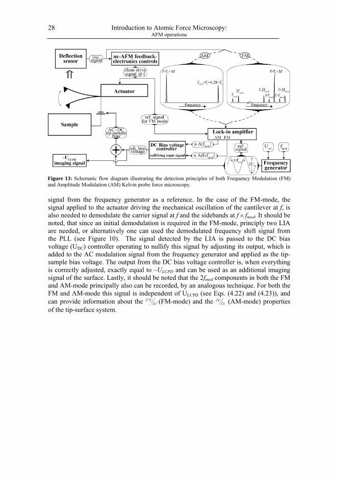
Tapping mode AFM As a hybrid mode between contact and non-contact AFM, tapping mode AFM (TM-AFM) [43] was introduced in 1993. TM-AFM is used in ambient or liquid environments, and it constitutes one of the key advances within AFM, finding a huge range of applications especially within the field of biology. Serving as an intermediate state of imaging between contact and nc-AFM, TM-AFM overcomes some of the inherent limitations and problems associated with either of the conventional AFM imaging modes. As the name implies, in TM-AFM the cantilever is oscillated so close to the surface, that the tip probes the strong repulsive region at the lower turning point of the oscillation cycle, in a sense tapping the surface. The detection scheme of TM-AFM is very similar to that of AM-AFM described previously, using a fixed driving frequency and measuring the tip-surface interaction from a change in oscillation amplitude, caused by the strong tip-surface interaction. Compared to contact AFM, TM-AFM overcomes the inherent risk of plastic deformation (damage) occurring either at the surface or at the tip, while still maintaining comparable spatial resolution. In fact, the lateral resolution is generally increased, since the lateral frictional forces and the coupled stick-and-slip motion of the tip present in contact AFM, are almost entirely removed. Also, using TM-AFM it is possible to image molecules, which are only loosely bound to the substrate on which they are deposited for imaging, without the risk of “scraping them away”, as in the case of contact AFM.
Compared to true nc-AFM, TM-AFM also has advantages. Under ambient conditions the humidity will form thin films of water on both the tip and the surface under inspection, resulting in what is known as capillary forces [44,45]. The capillary forces arise when the tip and surface come close to each other, i.e. at the lower turning point of the oscillation, as the water layers of the tip and surface form a meniscus bridge between the tip and surface. The capillary forces will cause a “jump-to-contact”, trapping the oscillating tip-cantilever system, which is obviously undesirable. This can be prevented by using TM-AFM, which is operable at greatly increased oscillation amplitudes, since the hugely increased tip-surface interaction strength compensates for the loss of sensitivity associated with large oscillation amplitude. The large oscillation amplitude of TM-AFM, increases the restoring force of the cantilever at the extreme positions, preventing a “jump-to-contact” from occurring. For a more general description of TM-AFM and its applications, and for a comparison of advantages and disadvantages see Ref. [38]
Introduction to Atomic Force Microscopy: AFM operations
20
4.4.3 Feedback loops Feedback loops controlling the tip-surface imaging distance are central components in any type of scanning probe microscopy. The feedback loop works in the following way. A measured feedback parameter, which is a distance dependent property of the surface, e.g. the tunneling current in STM, the absolute repulsive force in contact AFM, the change in oscillation amplitude in AM-AFM or the frequency shift in FM-AFM, is fed to a control unit which compares the measured value to a set-point value determined by the user. If there is a difference (an error) the controller adjusts the tip-surface distance to reduce the error. As the tip is raster scanned in a line-by-line fashion across the surface the feedback loop continuously adjusts the tip-surface distance making sure that the measured property of the surface is kept at a constant value. In the case of FM-AFM, the tip thus traces the surface on a contour of constant frequency shift, and the variations in the voltage applied to the z-piezo of the scanner tube, adjusting the tip-surface distance becomes the imaging signal. The voltage applied to the z-piezo along with xy-position of the tip over the surface determined by the voltages applied to the x- and y-piezo of the scanner tube, can then through appropriate calibration factors be used to generate a 3D real-space topographic image of the surface being imaged. The use of feedback loop has both pros and cons. It is practically impossible to align the surface to be scanned perfectly parallel to the xy-scanning plane of the tip, and when areas of a size of more than ~ 10×10 nm2 are being scanned, there is a huge risk of crashing the tip into the surface if no feedback loop is applied. The tip may also crash into atomic steps on single crystal surfaces, or deposited nanoclusters or molecules, and as such the z-feedback loop acts as a safety precaution, preventing destructive interactions. However, the use of a z-feedback loop does not come without a price. The continuous adjustment of the tip-surface distance can, if the feedback gain is set too high, cause the z-feedback loop to start to oscillate, introducing noise in the measurement. Also, as will be explained in the next section, additional channels are sometimes recorded simultaneously during FM-AFM imaging. These signals are also distance dependent, and if a z-feedback loop is applied, crosstalk will occur between the topographic imaging of the surface and the additionally recorded channels. (See Sections 6.5, 6.7 and 6.8 for experimental results)
4.4.4 Additional imaging signals This section will deal with the additional scanning probe imaging channels available when using the FM-AFM technique. As described in the previous sections, the primary imaging signal in FM-AFM is the measured detuning. If a z-feedback loop is used to adjust the tip-surface distance to maintain a constant detuning, the applied voltage to the z-piezo becomes the primary imaging signal. In either case, both signals are usually recorded. In addition, several other imaging channels are available.
Higher harmonics imaging When the tip is being oscillated in the force field of the surface, the potential felt by the tip is no longer harmonic and the motion of the cantilever can no longer be described by a single oscillation frequency. An accurate description of the cantilever oscillation then becomes a Fourier series, composed of a fundamental harmonic component and in principle an infinite number of higher harmonic components at integer multiples of the fundamental frequency. For large oscillation amplitudes, the amplitudes of the higher
Introduction to Atomic Force Microscopy: AFM operations
21
harmonic components of the Fourier series are simply proportional to the frequency shift detected, and hence they contain no additional information [46]. At small oscillation amplitudes, however, the amplitudes of the higher harmonics in the Fourier series provide additional information about the surface under inspection, being proportional to the corresponding derivative of the tip-surface force gradient, e.g. the amplitude of the second harmonic is proportional to the first derivative of the force gradient, etc. [47]. The amplitude of the higher harmonics can be monitored individually by lock-in techniques, and recorded as an additional imaging signal, providing additional information about the tip-surface potential. Alternatively the oscillation signal of the cantilever can be passed through a high-pass filter, removing the fundamental resonance frequency, and then passed through an RMS-to-DC converter producing a signal proportional to the sum of all higher harmonic amplitudes. Since each derivative made of the force gradient will cause it to decay faster, the outermost tip-apex atom will carry a larger and larger part of the interaction responsible for the corresponding higher harmonic oscillation amplitude. This increased weight of the tip-apex atom in the resulting signal will increase the spatial resolution of images made from higher harmonics amplitudes, as shown in Ref. [47].
Dissipation imaging The gain output of the “PID amplitude controller” (see Figure 10), provides information about how much energy is being dissipated in the cantilever oscillation. From the equation of motion of the tip-cantilever system in Eq. (4.7), it is evident that the cantilever has an intrinsic damping which dissipates the oscillation energy. To maintain a constant oscillation amplitude, energy must continuously be supplied by the oscillation actuator, and hence the gain output of the “PID amplitude controller”. From a Q-value measurement of the cantilever oscillation, the intrinsic energy dissipation per oscillation cycle (∆Eintr) can be estimated through the following expression using typical experimental parameters for:
( )1 22 N nmm2 eV
osc.
2energy stored in the oscillationenergy lost per radian
2 20 101.3
30000
cant
intr
cantintr
EQ
E
k AE
Q
π
π π
= = ⇔∆
∆ = = ≈
(4.16)
However, as the tip scans the surface, additional energy may be dissipated in the tip-surface interaction. This will force the output gain of the “PID amplitude controller” to increase, and hence an energy dissipation map of the surface can be recorded, by monitoring the output gain of the “PID amplitude controller”. If there are sites on the surface, where the tip-oscillation dissipates more energy, these will show up as bright spots or areas (depending of course on the color scaling) in the dissipation images. It is still being debated, which exact fundamental physical processes cause energy to be dissipated in the tip-surface interaction cycle. However, at present the most likely candidate seems to be what is commonly referred to as an adhesion hysteresis process. It involves a reversible deformation of the atomic structure of either the surface or the tip atoms, occurring within each oscillation cycle. This deformation changes the force map of the tip trajectory between approaching and retracting from the surface, resulting in a
Introduction to Atomic Force Microscopy: AFM operations
22
hysteresis loop, and hence a loss of energy. The situation where the deformation occurs at the tip, is depicted in Figure 11. Theoretical calculations of the energy dissipated through adhesion hysteresis, estimate values very similar to dissipation reported from experiments [48,49] (see also Section 6.8).
Another process causing energy to be dissipated in the tip-surface interaction, is stochastic friction. In a stochastic friction model of the tip-surface system, the tip can be described as a massive Brownian particle immersed in a “fluid” of much lighter particles, represented by the surface atoms, with the surface atoms dissipating the energy of the cantilever oscillation through thermal vibrations. However, theoretical studies and simulations of the stochastic friction model, produce dissipation energies several orders of magnitude too low, compared with experiments [50]. As such stochastic friction does not seem to be able to account for the experimental atomic scale contrast dissipation energies reported.
A much less discussed source of energy dissipation is the generation of Higher Harmonic Oscillations (HHO) in the cantilever, which occur due to the anharmonic potential imposed by the tip-surface interaction, as described in the previous section. These generated higher harmonics are located at frequencies of integer multiples of the fundamental resonance frequency (2×f0, 3×f0, 4×f0, etc.). Since the mechanical overtones of an oscillating cantilever with a rectangular cross-section (i.e. a beam) are located at non-integer multiples of the fundamental resonance frequency (6.27×f0, 17.55×f0, 34.39×f0, etc. [51]), the higher harmonics generated are subject to immense damping as there is no mechanical resonance phenomenon aiding the oscillation for the HHO. This implies that the energy stored in the HHO must be continuously supplied, as it is immediately dissipated into heat in the cantilever. This process thus constitutes a loss of energy within each oscillation cycle, which needs to by supplied by the “PID amplitude controller” and is hence visible in the recorded dissipation signal. It has been shown that the oscillation amplitude of the generated first HHO at 2×f0, in a large amplitude limit, are on the order of 2 - 3 orders of magnitude smaller compared with the amplitude of the fundamental oscillation amplitude [46]. A rough estimation for the energy dissipated through the first HHO can be made from typical experimental parameters: cantilever
Figure 11: Schematic drawing of a hysteresis loop occurring within an oscillation cycle, as rearrangements of the outermost tip atoms cause changes to the tip-surface force curve.
Introduction to Atomic Force Microscopy: AFM operations
23
spring constant ~20N/m, primary oscillation amplitude ~20 nm (peak-to-peak), with the amplitude of the first HHO reduced by a factor of 1000:
[ ]
Nm
22 10 nm1 1 20 6 meV
2 2 1000HHO cantE k A⎛ ⎞
∆ = = =⎡ ⎤ ⎜ ⎟⎣ ⎦ ⎜ ⎟⎝ ⎠
(4.17)
The number obtained using Eq. (4.17) is a very crude approximation. However, it shows that the order of magnitude of energy dissipated through the generation of HHO is within the range of what has been reported experimentally (see Section 6.8 and Refs. [48,49]), and as such it poses as a promising alternative to account for atomic scale dissipation, along side the more widely discussed dissipation mechanisms treated in this section.
Tunneling current images Above it was described how in the experimental setup, a bias voltage is applied between the tip and the surface, in order to minimize electrostatic effects. If the surface being imaged is slightly conducting, the bias voltage applied will cause a quantum mechanical tunneling of electrons (a tunneling current, It) to flow from the tip, through the vacuum gap, and into the surface (or vice versa). It is the exact same principle that lies at the origin of Scanning Tunneling Microscopy (STM) [1,52,53]. The current flowing is often expressed by this tip-independent, simple, and yet instructive expression which results from a classic quantum mechanical description of the electron tunneling process, with the vacuum gap modeled as a potential barrier [54]:
( ) ( )02
exp 2 where et t t
mI z I zκ κ
Φ= − =
h (4.18)
where z, κt me and Φ are the tip-surface separation distance, the tunneling current decay constant, the electron mass and the work function. If the experimental setup allows it, the It can be recorded simultaneously during the imaging of the surface as an additional imaging signal, providing information about the local electronic structure of the surface. In nc-AFM the tip is oscillated above the surface which of course affects the magnitude of the measured It, through its exponential distance dependence (Eq. (4.18)). However, most preamplifiers used to convert the It into a measurable voltage signal have a bandwidth in the 10 kHz range. This is much lower than the oscillation frequency of the cantilever, and as a result the measured It is averaged over the oscillation cycle. The connection between the maximum It (It,max) flowing when the tip is closest to the surface, and the measured averaged It (It,ave) can, in a large amplitude limit, be expressed as [55]:
,, 2
t maxt ave
t p p
II
Aπκ −
= (4.19)
where κt and Ap-p are the It decay constant and the cantilever peak-to-peak oscillation amplitude, respectively. This type of imaging will be described in more detail in Section 6.5.
Introduction to Atomic Force Microscopy: AFM operations
24
Kelvin Probe Force Microscopy As described briefly in section 4.3.1, when two bodies with different Fermi energies are brought into contact with each other, the electrons redistribute to accommodate the new joint Fermi level, with electrons from the higher Fermi level material flowing to the lower Fermi level material. Since the nuclei are fixed, this process results in a Contact Potential Difference (CPD [eV] = e × UCPD [V]) arising, which in turn results in an additional attractive contribution to the overall force. In the context of nc-AFM, this means that an additional contribution to the measured frequency shift exists, which in general is unwanted since it may have a strong influence on the topographic imaging as shown in Ref. [56]. The CPD contribution to the measured frequency shift can be derived from the expression for the force in Eq. (4.5) using the small amplitude approximation in Eq. (4.11):
( )
( )
20
220
2
12 2
4
CPD CPD biascant
CPD CPD biascant
f Cf U Uk z z
f Cf U Uk z
∂ ∂⎛ ⎞∆ = − −⎜ ⎟∂ ∂⎝ ⎠
∂∆ = − −
∂
(4.20)
where f0 and kcant are the free resonance frequency and the spring constant of the tip-cantilever system, C is the capacitance between the tip and the surface, and UCPD and Ubias are the contact potential difference and the applied bias voltage. As is evident from Eq. (4.20) the resulting additional frequency shift is proportional to -(UCPD - Ubias)2 meaning that it will be exactly equal to zero at Ubias = -UCPD and negative at all other applied bias voltages. This fact is utilized to determine -UCPD, with the purpose of cancelling out this contribution, by sweeping the applied Ubias and recording the resulting frequency shift at a fixed point above the surface. Data from such a measurement is presented in Figure 12, where Ubias was ramped from -2 to 3 V. The parabola shape of the recorded frequency shift curve reflects the squared dependence on Ubias, with the value at the vertex being equal to -UCPD. In this way, the value of the applied Ubias, which exactly cancels out the effect of the CPD can be determined prior to recording topographic images of the surface under inspection. However, this only works for electrically homogeneous metallic and semi conducting surfaces. For insulators electrons are not free to move and the concept of a Fermi energy is not well defined. There may,
Figure 12: Experimentally recorded spectroscopy curve showing the parabolic bias voltage dependence of the frequency shift. The voltage corresponding to the parabola apex is identified as the contact potential difference.
Introduction to Atomic Force Microscopy: AFM operations
25
however, still be a non-zero bias voltage at which the electrostatic forces are cancelled out, e.g. from surface charging effects [57]. Complex and electrically inhomogeneous systems such as metal nano-particles deposited on single crystal surface, may also have additional local contributions to the overall intrinsic potential difference between the tip and the surface. This can be expressed by introducing a Local Contact Potential Difference (LCPD [eV] = e × ULCPD [V]) term:
( )2
where( , , )
CPD LCPD bias
LCPD CPD add
f U U
U U U x y z
∆ ∝ − −
= + (4.21)
where all additional contributions to the intrinsic CPD between the tip and the sample are included in Uadd. Uadd may be a non-local function of the (x,y) position of the tip over the surface, and also of tip-height over the surface (z). The z dependence comes from the fact that Uadd is a local electrostatic effect, which at large separation distances is averaged out, and as such is only detectable at small separation distances. The exact composition of ULCPD must be evaluated for the individual system, but the important point here is just to notice that in general ULCPD is not a constant value across the entire surface. This means that the method for determining the required Ubias to cancel out ULCPD no longer works, and that a new technique, namely the Kelvin Probe Force Microscopy (KPFM) method, needs to be employed. The KPFM method is derived, as the name implies, from an experimental technique introduced as early as in 1897 by Lord Kelvin [58]. There, Kelvin was able to detect on a macroscopic scale, the electrostatic force induced deflection in a so-called Volta condenser, caused by the formation and breaking of electrical contact between two different metals (copper and zinc). The modern version of Lord Kelvin’s original experimental setup, the Kelvin Probe Force Microscope, is slightly more sophisticated. However, it is driven by the same fundamental physical laws, namely the intrinsic CPD existing between two materials with different work functions in electrical contact.
The “modern” KPFM technique works by adding a modulating AC bias voltage (Umod = UAC × sin(2πfmodt)) to the DC bias voltage (UDC) applied between the surface and the oscillating tip-cantilever system. In the approximation that only the capacitance has a non-zero gradient, the resulting electrostatic force between the tip and the sample can be written (see Eq. (4.5)):
( )( )
( ) ( )
( ) ( )
( )
2
2
2 2
22
1 sin 22
where1 12 2
1 2 sin 22
1 1 sin 2 22 2
mod mod
mod
mod
el LCPD DC AC mod
el DC f f
DC LCPD DC AC
f LCPD DC AC mod
f AC mod
CF U U U f tz
F F F F
CF U U Uz
CF U U U f tz
CF U f tz
π
π
π
∂= − −
∂= + +
∂ ⎛ ⎞= − +⎜ ⎟∂ ⎝ ⎠∂
= − −∂∂
=∂
(4.22)
Introduction to Atomic Force Microscopy: AFM operations
26
Eq. (4.22) reveals that there are now three distinctive contributions to the electrostatic force acting between the tip and the surface: FDC (a constant DC term), Ffmod (a term oscillating at frequency fmod) and F2fmod (a term oscillating at frequency 2fmod). There are now two ways of utilizing the result in Eq. (4.22) to adjust UDC in order to exactly cancel out ULCPD. In both methods, the UDC applied to the surface can be recorded, providing a local contact potential measurement (UDC = -ULCPD), as well as a correct topographical image of the surface, which finds applications in fields such as semi-conductor physics, photo-catalysis, etc. For a detailed introduction to KPFM imaging and its applications see Refs. [17,59,60].
KPFM amplitude modulation mode In the KPFM Amplitude Modulation mode (KPFM AM-mode), the detection system is tuned to detect the electrostatic forces between the tip and the surface. The Ffmod and F2fmod terms in the electrostatic force in Eq. (4.22) will drive the cantilever oscillation at fmod and 2×fmod respectively, superimposed on the mechanical oscillation at its resonance frequency. The oscillation amplitude signal at fmod will be proportional to ULCPD - UDC and can be detected using a Lock-In Amplifier (LIA). The signal is then fed to a control circuit which operates continuously during scanning of the surface, in order to nullify this signal by adjusting the UDC applied to the surface. In this way UDC is constantly kept equal to – ULCPD, minimizing the electrostatic interactions. However, from Eq. (4.22) it is evident that even at UDC = -ULCPD the electrostatic forces are not completely cancelled as the FDC term depends linearly on (Umod)2. This means that Umod should be kept at a minimum, especially on semi conducting surfaces, where a too large electrostatic potential difference between the tip and the surface can induce band-bending, creating artifacts [61]. However, since the detected oscillation signal at fmod also depends linearly on Umod, a lowering of Umod results in a decrease in the signal-to-noise ratio (S/N). By tuning fmod to the first overtone of the mechanical resonance frequency of the cantilever (given approximately by f1 ~ 6.27×f0 [37]) the oscillation amplitude is increased by the corresponding Q-value of the first overtone oscillation (Q1), increasing the S/N drastically. Q1 is, however, normally significantly lower compared with the Q-value of resonance frequency oscillation (Q0) (we and others [62] have found Q1 ~ 8000 in UHV, whereas Q0 normally lies within the 25000 - 50000 range). Using the KPFM amplitude modulation mode, variations as low as 2 mV in the KPFM have been reported as detectable in the measured LCPD signal [61]. There are, however, still drawbacks. For high resonance frequency cantilevers (f0 ~ 250-350 kHz) the first overtone (f1 ~ 1.5-2.2 MHz) usually lies above the bandwidth of the oscillation detection electronics, and low resonance frequency (~70 kHz) cantilevers need to be applied. This gives rise to a decrease in the S/N for the topography imaging since the measured ∆f, which is the primary imaging signal, decreases with a decreasing resonance frequency of the cantilever (see Eqs. (4.11) and (4.12)).
Introduction to Atomic Force Microscopy: AFM operations
27
KPFM frequency modulation mode In contrast to KPFM AM-mode, the KPFM frequency modulation mode (KPFM FM-mode) detection scheme is tuned to detect the electrostatic force gradient. The expression for the electrostatic force in Eq. (4.22) will affect the frequency shift of the tip-cantilever system, modulating it with frequency components at fmod and 2fmod. Using the small amplitude approximation from Eq. (4.11) the frequency shift caused by the electrostatic forces in Eq. (4.22) can be written:
( )
( ) ( )
( ) ( )
( )
02 2
22 20
2
20
2
220
2 2
2where
1 12 2 2
cos 22
1 cos 2 22 4
mod mod mod mod
mod
mod
EL DC f f DC f fcant
DC LCPD DC ACcant
f LCPD DC AC modcant
f AC modcant
ff F F F f f f
k z
f Cf U U Uk zf Cf U U U f t
k zf Cf U f t
k z
π
π
∂∆ = − + + = ∆ + ∆ + ∆
∂
∂ ⎛ ⎞∆ = − − +⎜ ⎟∂ ⎝ ⎠
∂∆ = −
∂
∂∆ = −
∂
(4.23)
The ∆ffmod and ∆f2fmod contributions to the total frequency shift appear as sidebands at f ± fmod and f ± 2fmod, respectively, in the frequency spectrum of the cantilever oscillation signal. Using a lock-in amplifier (LIA) it is possible to measure the signal at f ± fmod. This signal can, like in the KPFM AM-mode, be nullified by adjusting UDC, thereby minimizing the electrostatic forces. There is, however, still, as in the KPFM AM-mode, a DC contribution from the electrostatic forces, even at UDC = -ULCPD, which is undesirable for the same reasons as listed in the previous section. The KPFM FM-mode has a few advantages compared with the KPFM AM-mode. The measurement of the ULCPD is for the FM-mode proportional to 2
2C
z∂
∂ , whereas in the AM-mode it is proportional to Cz
∂∂ ,
which theoretically should give the FM-mode a higher spatial resolution. Also, since the FM-mode operates with significantly smaller fmod (typically ~1 kHz) high resonance frequency cantilevers can be applied without exceeding the bandwidth of the detection electronics, providing better topography resolution. There are, however, also disadvantages to using the FM-mode. Since the FM-mode does not operate by detecting an oscillation amplitude, the resonance enhancement of operating at overtone frequencies, is absent, and compared with the AM-mode the S/N is reduced by factor of order of Q1 ~ 8000!! This means that a larger modulation frequency amplitude (UAC) needs to be applied to get an adequate S/N, which, as mentioned earlier, can cause undesirable effects.
Detection schemes In Figure 13 a schematic drawing of the detection schemes used in the AM-mode and FM-mode, is depicted. The modulation signal is provided by a frequency generator at a constant amplitude (Umod) and frequency (fmod). The frequency spectrum of the oscillation signal is shown schematically for both AM and FM-mode. The Lock-In Amplifier (LIA) detects the signal at fmod (AM-mode) or f ± fmod (FM-mode) using the
Introduction to Atomic Force Microscopy: AFM operations
28
signal from the frequency generator as a reference. In the case of the FM-mode, the signal applied to the actuator driving the mechanical oscillation of the cantilever at f, is also needed to demodulate the carrier signal at f and the sidebands at f ± fmod. It should be noted, that since an initial demodulation is required in the FM-mode, principly two LIA are needed, or alternatively one can used the demodulated frequency shift signal from the PLL (see Figure 10). The signal detected by the LIA is passed to the DC bias voltage (UDC) controller operating to nullify this signal by adjusting its output, which is added to the AC modulation signal from the frequency generator and applied as the tip-sample bias voltage. The output from the DC bias voltage controller is, when everything is correctly adjusted, exactly equal to –ULCPD and can be used as an additional imaging signal of the surface. Lastly, it should be noted that the 2fmod components in both the FM and AM-mode principally also can be recorded, by an analogous technique. For both the FM and AM-mode this signal is independent of ULCPD (see Eqs. (4.22) and (4.23)), and can provide information about the 2
2C
z∂
∂ (FM-mode) and the Cz
∂∂ (AM-mode) properties
of the tip-surface system.
Figure 13: Schematic flow diagram illustrating the detection principles of both Frequency Modulation (FM) and Amplitude Modulation (AM) Kelvin probe force microscopy.
Introduction to Atomic Force Microscopy: Difficulties faced by AFM
29
4.5 Difficulties faced by AFM 4.5.1 Monotonicity and distance dependence Generating a topographic image of a surface using a feedback loop is done by measuring a property of the surface, and then using an a priory knowledge about whether the measured property increases or decreases with distance. If the value of the measured property differs from a setpoint value, the tip-surface distance is adjusted accordingly. In the case of STM this proves particularly easy, where the measured property is the magnitude of the tunneling current (It) flowing between tip and surface. Since the It decays exponentially with distance (see Eq. (4.18)), the feedback loop approaches the tip if the measured It is lower than the setpoint value and vice versa. Also, the exponential distance dependence of the It, makes for a large signal-to-noise ratio (S/N), with the It dropping by one order of magnitude when the tip-surface distance is increased by 0.1 nm. (using typical values in Eq. (4.18)).
In AFM things are not as simple. As is evident from the graph in Figure 7, neither the force and consequently nor the force gradient depend in a monotonic way on the tip-surface separation distance. This means that when imaging the surface in e.g. FM-AFM, where the measured frequency shift is coupled directly to the tip-surface force gradient, the parameter space in which the frequency shift setpoint can be chosen is restricted to either negative or positive frequency shifts as indicated in Figure 7. For the negative frequency shift region, the tip-surface distance is further restricted to stay on the monotonic part of the curve as indicated by the gray background shaded region. Since the tip-surface force gradient curve changes shape depending on the micro- and macroscopic shape of the tip, the maximum attainable negative frequency shift is unknown. This has the consequence that when probing in the attractive regime, which is the most common mode of operation, and the negative frequency shift setpoint is set above the maximum attainable value, the feedback loop crashes the tip into the surface, potentially destroying the tip. There are ways around this problem by using a rectifier on the detected frequency shift. The distance dependence of the frequency shift in nc-AFM, is determined by both short and long-ranged forces (see Section 4.3), where only the short-ranged forces have an exponential distance dependence, equivalent to that of the STM. The long-ranged forces are typically governed by inverse power law dependencies reducing the atomic scale sensitivity of the nc-AFM and hence reducing the S/N.
4.5.2 Stability and noise Many factors come into play when considering the optimal experimental parameters in term of signal-to-noise and stability, and for nc-AFM experiments in particular, many of these are in conflict, as will be illustrated in this section.
When the nc-AFM tip oscillates in close proximity of the surface there is a risk that the tip snaps into contact with the surface due to the long- and short-ranged attractive force. This is obviously undesirable, and it puts a restriction on the mechanical aspects of the cantilever and its oscillation. The restoring force of the cantilever must be greater than the maximum attractive tip-surface force (max(Fts)) [40], or alternatively, the cantilever spring constant must be greater than the maximum tip-surface force gradient (max(kts)) [63]. This can be expressed as:
Introduction to Atomic Force Microscopy: Difficulties faced by AFM
30
( )max( ) or maxcant ts cant tsk A F k k> > (4.24) where kcant, and A are the cantilever spring constant and oscillation amplitude, respectively. Eq. (4.24) puts lower limits on the cantilever spring constant and the oscillation amplitude.
If considering only Eq. (4.13), it is evident that the measured frequency shift increases, increasing the signal-to-noise (S/N) ratio, with decreasing oscillation amplitude and cantilever spring constant. However, the lowering of both these experimental parameters is prohibited by several restrictions. Thermal noise induced in the cantilever oscillation affects the accuracy with which the oscillation frequency, and hence the frequency shift, can be measured. The noise in the frequency measurement caused by thermal noise has been shown to have the following form [15]:
02
Bthermal
cant
f k TBf
k A Qδ
π= (4.25)
where T, B, kcant, A, f0 and Q are the temperature, the detection bandwidth, the cantilever spring constant, oscillation amplitude, resonance frequency and Q-value, respectively. From Eq. (4.25) it is seen that the thermal noise decreases with increasing kcant and A. This dependency can be understood intuitively since the energy stored in the cantilever increases with increasing kcant and A, making it less affected by the thermal “noise-kicks” of energy kBT. The increase in the thermal noise, coming from decreasing kcant and A, counteracts the increased frequency shift signal gained through Eq. (4.13). However, the thermal noise limit in Eq. (4.25) is a lower theoretical limit, and the detection noise, e.g. noise in the photo detector (if one is used), electronic circuits, etc., is often much greater than the thermal noise. The frequency shift noise originating from the detection noise can be shown to have the following dependence [64]:
3
2 ; cantdetection
znf B nA B
δδ
π= = (4.26)
where δz and n are the noise in the cantilever oscillation signal and the corresponding noise density, respectively. Comparing Eq. (4.26) with Eq. (4.25) the main important difference is the dependence on B. For the detection noise the frequency noise scales as B3/2, and with the detection noise being the dominating factor, this makes B a crucial parameter in nc-AFM measurements, calling for slow scanning speeds when aiming for high resolution.
The dependence on A in Eq. (4.13), with the signal ∆f increasing with decreasing A, compared with Eq. (4.26), which shows an increase in the noise δfdetector with decreasing A, indicates that there exists an optimal A at which the S/N reaches a maximum. This optimal A has been shown to be approximately the interaction distance of the short-ranged chemical forces i.e. in the 0.1 nm range [65]. To enable such small A, requires very stiff cantilevers, in order to avoid the occurrence of instabilities (Eq. (4.24)). This has been successfully realized by Giessible et al., who introduced the use of very stiff quartz cantilevers, the so called q-plus, which allow for sub-nanometer oscillations amplitudes [66]. Another recent development was presented by An et al. using a quartz Length Extension Resonator, also enabling atomic resolution at sub-nanometer
Introduction to Atomic Force Microscopy: AFM Simulations
31
oscillation amplitudes [67]. Also, it has recently been shown that even sub-Angstrom oscillation amplitudes are attainable, using bent tungsten wires as cantilevers and an optical interferomitry detection setup [68].
4.6 AFM Simulations Since AFM images, and SPM images in general, do not explicitly contain any information regarding the chemical nature of the substrate under inspection, it is often desirable to simulate what AFM images should look like of a specific substrate, and then from a comparison with the experimental data, identify the chemical composition. To do so, requires not only a model of the substrate, but also a model of the AFM tip.
4.6.1 The surface and tip models The surface model is in principle an exact atomic model of the entire crystal to be simulated. However, since the number of atoms in a real physical crystal is, for all practical purposes, infinite, a few approximations and tricks are applied. In the direction perpendicular to the surface, the surface model can be reduced to include only the top-most atomic layers, since the interactions in nc-AFM producing atomic scale contrast are short-ranged in nature. When the crystal was cut to form a surface, the local environment for the top-most atomic surface layers changed (nearest and next-nearest neighbors disappeared), causing the atoms to adjust their positions (relax), in order to find their new energy minimum. This means that the surface model, cannot be constructed exclusively from bulk lattice vectors, which are generally available from diffraction type experiments, e.g. LEED. To circumvent this problem, the surface model is constructed from several, typically 3 – 10, of the topmost atomic layers, with only the “bottom” atomic layer kept fixed at crystal bulk positions. All other layers are allowed to relax, to find their new positions minimizing the energy, as will be described later. In the plane of the surface the number of atoms can also be reduced by considering only the atoms within a surface unit-cell and by applying periodic boundary conditions. The above approximations reduce the number of atoms required to make up the surface model from “infinite” to typically on the order of 50.
The tip is, like the crystal described above, a macroscopic object also consisting of an “infinite” number of atoms. However, as for the case of the surface model, only the outermost tip atoms are required to account for the short-ranged chemical forces, governing the atomic scale image contrast. In this respect, the tip is often modeled as an atomically well-defined small nano cluster, consisting typically of a few tens of atoms, of a chemical nature relevant for the experiment at hand.
To account for the long-ranged van der Waals (vdW) the atomic scale surface and tip models are embedded into a semi-infinite uniform box and a uniform cone truncated with a semi-sphere (typically), representing the bulk material of the crystal and the tip, respectively. The box and cone-sphere have no atomic structure, and are described only by macroscopic parameters (density, polarizability, etc.). They are used to calculate the vdW contribution to the total interaction energy, principally using through Eq. (4.3)
4.6.2 The simulation Once the tip and surface models are in place, a scheme to calculate the interaction force needs to be decided on. One approach, known as Atomistic Simulations (AS), is to
Introduction to Atomic Force Microscopy: AFM Simulations
32
model all atoms, in both the tip and the surface models, as consisting of a positive point charge representing the nucleus, and a negative spherical shell representing the electron cloud. Each of the point charges and electron shells are given the position vectors ri
nuc.
and rie.s., respectively. The interaction energy can then be calculated by summarizing the
following contributions:
1. Each pair of nucleus and electron shell is connected by a spring-type force with spring constant katom, allowing the atoms to become slightly polarized, but keeping them from “falling apart”.
2. All nuclei and electron shells interact electrostatically depending on their respective charges Qnuc. and qe.s..
3. To account for non-electrostatic interactions between the atoms, a two-body potential is set up‡‡, describing Pauli repulsion and long-ranged vdW interaction.
Writing each contribution explicitly produces the following expression for the total interaction energy:
{ }
.
2. . .
. . . . . . . . . . . ..
. . . . . . . . . .0
1 22
where
12
14
all atomsspring electr short
i i ii
nuc e sspringi ii atom
nuc nuc nuc e s e s nuc e s e si j i j i j i jelectr
i nuc nuc nuc e s e s nuc e si j i j i j i
E V V V
V k r r
Q Q Q q q Q q qV
r r r r r r r rπε
= + +
= −
= + + +− − − −
∑
r r
r r r r r r r r
. .
. . . .
6. . . .exp
all atoms
e sj ì j
e s e sall atoms i jvdW
short Paulii Paulie s e sj ì i j
r rCV Cr r κ
≠
≠
⎧ ⎫⎪ ⎪⎪ ⎪⎨ ⎬⎪ ⎪⎪ ⎪⎩ ⎭
⎧ ⎫⎛ ⎞−⎪ ⎪⎜ ⎟−⎪ ⎪= + −⎜ ⎟⎨ ⎬⎜ ⎟⎪ ⎪⎜ ⎟−⎪ ⎪⎝ ⎠⎩ ⎭
∑
∑r r
r r
(4.27)
The parameters that go into Eq. (4.27), e.g. katom, position vectors, CvdW, etc., must either be derived from (or fitted to match) existing experimental data or calculated using a ab initio Density Functional Theory (DFT) approach (described in the following). Care must, however, be taken not to produce artificial interactions, e.g. by using bulk properties of a crystal that do apply to the surface, like for instance atomic positions. Considering the complexity of atomic interactions with overlapping electronic orbitals, this is of course a very simple model, and it is therefore only applicable to systems which exhibit pronounced ionic character, e.g. metal-oxides.
When the system becomes more metallic, the valence electrons become more delocalized and are free to move around to minimize their energy, causing the expression
‡‡ The one used here is known as the Buckingham two-body potential.
Introduction to Atomic Force Microscopy: AFM Simulations
33
in (4.27) fails. In this case, the full many-body Schrödinger equation for the entire system needs to be solved, which is usually done using DFT. For more details on this see Refs. [22,69]. This approach is considered as ab initio modeling, as it, in principle, contains no parameterization, and requires only the atomic number of the elements involved. In this sense the DFT approach is generally considered to be more accurate or true, compared with AS. However, AS calculations are far less computationally expensive compared with the ab initio DFT approach. AS, containing hundreds of atoms, can easily be run on a standard desktop computer, whereas the DFT approach requires super-computers for equivalent systems.
Regardless of how the interaction energy is calculated, the resulting forces can be derived from it. The calculated forces are used initially to relax the structure of the tip and the surface separately, with “top-most” atomic layer in the tip, and the “bottom-most” atomic layer in the surface unit-cell slab, kept fixed (frozen), to mimic the transition to the macroscopic bulk material. Then the tip is moved in a step-by-step fashion through as many points in the three dimensional space above the surface unit-cell as possible (limited primarily by the computation time). After each step all atoms in the tip and surface (except the frozen layers) are allowed to relax, after which the total force acting on the frozen part of the tip is calculated. In this way, a three dimensional force map is generated, and can be used to calculate the theoretical frequency shift at any point in the unit-cell, with given “experimental” parameters such as cantilever spring constant, oscillation amplitude, etc., using for instance the expression in Eqs. (4.11) or (4.13).
Introduction to Atomic Force Microscopy: AFM Simulations
34
35
5 Experimental details The work presented in this thesis has all been carried out, using a commercial Ultra High Vacuum (UHV) Omicron [70] variable temperature AFM/STM. The complete UHV AFM/STM system was supplied in December 2003, and has since then undergone some rather considerable modifications to improve its performance, in which I have been heavily involved. The following sections contain a short description of the microscope setup, along with a description of some of the programs that I have written, in order to control various processes in the laboratory. Also presented is a description of the experimental problems encountered during my PhD studies, along with their solutions.
5.1 The Omicron UHV system and AFM microscope
The UHV system has undergone some rather dramatic changes since it was delivered in December 2003. In Figures 14a and 14b two images of the chamber as it stands now (September 2007) are shown. The UHV system consists of two main chambers, one for surface preparation, Low Energy Electron Diffraction (LEED), Auger Electron Spectroscopy (AES, not indicated) and X-ray Photoelectron Spectroscopy (XPS) analysis (main preparation chamber), and one containing the Omicron AFM (main analysis chamber). Various items are labeled with numbers and the list below contains the corresponding descriptions matching these numbers:
1) XYZ manipulator for transferring samples (and tips) from the preparation chamber to the analysis chamber.
2) Pumping line to turbo molecular pump. 3) Power supply cable for annealing filaments. 4) Quadrupole mass spectrometer. 5) Ion-bombardment equipment. 6) Pyrometer for sample surface temperature indication. 7) Main preparation chamber. 8) High power LED for AFM detection. 9) Pumping line to ion-pump and Titanium Sublimation Pump (TSP). 10) Main analysis chamber containing the Omicron AFM microscope. 11) LEED analysis hardware. 12) AFM pre-amplifier. 13) Gas-inlet manifold. 14) Fast entry load-lock and transfer arm. 15) X-ray source for XPS analysis
The LEED, XPS and AES units are the very latest additions to the UHV system, and I have not been involved in the setting up or operation of these units. The LEED AES and XPS units will not be discussed further, and are mentioned here only for the sake of completeness. The gas-inlet manifold (13) is supplied from a gas-inlet system consisting
Experimental details: The Omicron UHV system and AFM microscope
36
of five different ultra pure gasses, allowing the dosage of various relevant gasses onto the sample surface (by chamber backfilling). Also, a gas dosage tube mounted on a Z-translator supplied from the gas-inlet system (not indicated) has been added to the chamber, allowing for dosing gas very close to the sample surface, providing a high local partial pressure of the respective gas. Additionally, the ion-bombardment sputtering unit is also supplied with argon gas from this gas-inlet system.
In Figure 14c an image taken through the large viewport in Figure 14a is shown. The picture shows the AFM microscope with the top of the scanner tube just visible with the mounted AFM cantilever and tip. Above the tip, sits a sample holder facing down, exposing the clean sample surface ready for experiments to the sharp AFM tip. During scanning the entire AFM microscope hangs suspended from three metal springs. The function of these springs is to isolate external vibrations (acoustic, building vibrations, turbo-pump noise etc.) from coupling into the AFM measurement, and they therefore have very low resonance frequencies of only 1 - 2 Hz. Additionally, the AFM microscope has U-shaped copper plates mounted on the outside of the base platform (three are indicated), which together with the magnets fixed to the UHV chamber form an eddy current damping system, also designed to remove/reduce external vibrational noise sources. A particularly useful thing about the Omicron AFM microscope design is
Figure 14: (a) and (b) Two images taken of the UVH system, with numbered labels (description are provided in the text) indicating the most important features. (c) Real picture taken through the large view-port in (a) as indicated. The top of the scanner tube along with the AFM tip-cantilever and tip-cantilever holder are indicated. Above the tip sits a sample holder “upside-down” facing sample surface down. Also indicated are three copper U-shaped plates used for eddy current damping. (d) Schematic drawing of the AFM microscope showing the laser, the laser beam alignment mirrors and optics, the position sensitive photo detector, the scanner tube and the AFM cantilever and tip.
Experimental details: Detection optics and light source
37
the fact that the microscope AFM tip can be changed in situ, without the need to breach the chamber UHV environment. As the life of an AFM tip is relatively short, it has been a great advantage to be able change the microscope tip quickly and easily (see also Section 5.4). The Omicron AFM microscope is an optical beam deflection type microscope, which uses the geometric amplification of an incident light beam reflected from the backside of the vibrating cantilever to detect the cantilever motion. The optical path that the light beam travels amplifies the nm oscillation amplitude of the cantilever, before it is detected by a Position Sensitive Photo Diode (PSPD). A schematic drawing of the AFM microscope is presented in Figure 14d, which shows in detail the optical path that the light beam travels, along with alignment mirrors and optics used for positioning the light beam accurately on the backside of the cantilever. The end point for the laser beam is the PSPD which detects the deflection / oscillation of the cantilever as it vibrates (see also Figure 15).
5.2 Detection optics and light source The light source for the deflection detection optics is a very important piece of equipment. The reason for this can be understood by considering the schematic drawing depicted in Figure 15, showing the principle behind the cantilever oscillation detection scheme employed in the Omicron AFM. A beam of light is directed onto the backside of the cantilever, in such a way that the reflected beam hits a Position Sensitive Photo Diode (PSPD). The PSPD is divided into four quadrants labeled A-D in Figure 15. The intensity of light hitting each quadrant (IA-ID) generates four signals which are fed into an electronic circuit which subtracts the sum of the upper half quadrants (A+B) from the lower half quadrants (C+D). The output from this electronic circuit is then proportional to the oscillation amplitude of the cantilever and is fed into the Constant Oscillation Amplitude Controller (COAC, see Figure 10). However, the output signal is not only proportional to the oscillation amplitude, but also to the total intensity of the initial light beam (I0). This means, that if I0 changes, then the COAC will detect this as a change in the physical oscillation amplitude of the cantilever, and adjust it accordingly. When the physical oscillation amplitude is changed by the COAC, e.g. increased, the AFM tip will come closer to the surface, and the constant detuning feedback loop will retract the tip to maintain a constant detuning. In this way, noise in the absolute intensity of the light beam is coupled directly into noise in the detected topographic signal. This is something which has caused significant experimental difficulties. The initial light source delivered with the microscope, a solid state laser, had a severe tendency to jump between different
Figure 15: Schematic illustration of the cantilever detection principle in the optical beam deflection scheme.
Experimental details: Detection optics and light source
38
lasing modes (mode-jump), changing its total output intensity continuously. Presented in Figures 16a, 16b, and 16c are an nc-AFM topography image (Z), the
simultaneously recorded sum of all four PSPD quadrants (Itot = IA+IB+IC+ID) and a cross-section graph taken along the black solid line in Figure 16b, respectively. The Itot signal in Figure 16b is of course proportional to the output intensity of the light source, and as is evident, Itot is not constant but jumps frequently, as is indicated even more clearly is the cross-section graph in Figure 16c. Labeled in the cross-section graph and in both images are single mode-jumps (J), and instabilities (I, several consecutive mode-jumps). The crosstalk from the light source noise into the nc-AFM topography channel is evident. The noise in Itot is not overwhelming, only around 0.2%, but as Figure 16 clearly shows, this noise level needs to be significantly lower! Two of the main reasons why the initial solid-state laser mode-jumped were temperature changes and light which got reflected back into the laser cavity. Therefore, the initial laser was replaced by a temperature stabilized laser which was also shielded from back-reflections into the laser cavity using an optical isolator. This new laser, did not show any sign of mode-jumping, however, it had a very low 50 Hz noise level (<0.1%), but enough so that it coupled into the nc-AFM topography images. A curious thing was that fact that at standard nc-AFM scanning speeds the 50 Hz noise from the laser sometimes looked very much like atomic resolution, making it somewhat difficult to identify. Finally, a high power LED was employed, and this has been working well. However, with the new band-passed filtered home build pre-amp described in Section 5.2, it might be worth testing the temperature stabilized laser again, as the smaller spot-size achievable using a laser compared with the LED should reduce noise from light reflected from elsewhere than from the cantilever. An important point to be made here, is the fact that unless the total output intensity of the light source used is actually monitored, it is very difficult to identify any noise as originating from the light source, as the noise in the image in Figure 16, is something that could also be the result of tip-instabilities.
Figure 16: (a) Topographic nc-AFM image of the TiO2(110) surface. (b) Simultaneous recorded total intensity detected by the PSPD. (c) Bottom-to-top cross-section of (b) taken along the solid vertical black line. Regions of intensity instabilities and jumps are clearly visible in (b) and (c), and the resulting noise introduced in the topographic image is very pronounced.
Experimental details: Pre-amplifier
39
5.3 Pre-amplifier The cantilever oscillation signal is fed directly from the PSPD to a feed-through on the UHV chamber. The raw signal detected is very small, and therefore extremely vulnerable to external noise. Therefore, mounted directly on ambient side of the feed-through, is an amplifier to boost the detected signal and minimize the effect of external noise sources, of which there are a countless number in any research laboratory. This amplifier, known as a pre-amplifier or in short just pre-amp., amplifies the signal prior to it traveling through wires and connections before entering the main measurement electronics, making it less affected by any noise pick up. To optimize the overall performance of the AFM microscope, an attempt has been made to construct a new pre-amp. with a better signal-to-noise ratio (S/N). The following list contains the most important improvement aspects:
• The overall design of the electronic circuit was made more compact, and features not needed for nc-AFM operation were eliminated.
• In the Omicron design the pre-amp. also acts as power supply for the PSPD, supplying a DC bias voltage of 10 V. The supply voltage noise was reduced slightly.
• The Printed Circuit Board (PCB) on which the different electronic components making up the pre-amp., are mounted, was changed to a 4 layer PCB. One of the middle layers was grounded, acting as a shield, allowing for the separation of different signals on the PCB, significantly reducing any risk of crosstalk occurring.
• In total, three outputs from the pre-amp. are needed: The AC-part of the signal recorded by the PSPD carrying the cantilever oscillation signal, the DC-part of the signal recorded by the PSPD to help with the initial aligning of the laser beam, and a DC-signal carrying the total intensity recorded by the PSPD, to help also with the laser beam alignment and to help to adjust the laser power. These three signals are all provided at the same pre-amp. output in the Omicron design, but split into three separate outputs in the new home-built design.
• The AC-part of the signal recorded by the PSPD is band-pass filtered with a center frequency close to 300 kHz, as this is the typical resonance frequency of the cantilevers used.
In Figure 17 a comparison of the AC-part of the new home-built pre-amp. (red) is compared with the equivalent signal from the original Omicron pre-amp. (black). The main graph shows two traces from 0 to 500 kHz. The bell-shape of the red curve reflects the band-pass filter applied, as mentioned above. To make a comparison meaningful, it is imperative that the physical oscillation amplitude of the cantilever is identical when recording the two traces. The Constant Oscillation Amplitude Controller (COAC) responsible for maintaining a constant oscillation amplitude of the cantilever, might respond differently to the two different pre-amps., and hence result in slightly different physical oscillation amplitudes. Therefore, the COAC was disabled, leaving only thermal excitation as the source of energy input to the cantilever oscillation, making for identical oscillation amplitude for the two traces. The level of the noise floor is approximately equal for both pre-amps., when considering only the region close to the oscillation peak, which is the region important for the frequency shift measurement. A
Experimental details: Pre-amplifier
40
zoom-in of the oscillation peak, shown in the inset, reveals that the new home-built pre-amp. (red) produces a ~4 dBm better S/N compared with the Omicron (black), corresponding to an increase of ~60 % in the oscillation amplitude signal produced by the pre-amp. This increase is not much. It is, however still an increase, and should provide for a better frequency shift measurement.
Additionally, the COAC is also affected by noise in the cantilever oscillation signal, since noise in the oscillation amplitude is translated directly into noise in the topographic image recorded (an example of this will be show in Section 5.2). Whereas the frequency shift measurement is sensitive to noise in a narrow region around the oscillation frequency, the COAC is sensitive to low frequency noise. With the imposed band-pass filter applied in the home-built pre-amp it should intuitively have a lower noise level at lower frequencies, compared with the Omicron pre-amp.
A better improvement in the S/N could likely be achieved by moving the pre-amp. into the UHV system, so that it sits very close to the PSPD. This would have two effects. Firstly, it would reduce the noise picked up by the wires carrying the oscillations signal from the PSPD to the feed-through. Secondly, it would reduce the input capacitance imposed by wires connecting the pre-amp. to the PSPD, which in the present setup are responsible for approximately half of the total input capacitance of ~50 pF. The input capacitance is extremely important for the noise produced by the input operational amplifiers in the pre-amp, and reducing this capacitance would significantly lower the noise output of the pre-amp., and hence increase the S/N. However, to move the pre-amp. into the UHV chamber imposes restrictions as to which components can be used, as the entire pre-amp must be UHV compatible, also under bake-out temperatures (~150 °C). In addition to this comes the practical challenge of making the pre-amp. fit and fixing it close to the PSPD. There are at this point no plans for moving the pre-amp. into the UHV, but it would perhaps be a project worth considering in the future.
The new home-built pre-amp. was just recently finished, and has therefore not been extensively tested under real experimental conditions, i.e. scanning a real surface.
Figure 17: Spectrum analyzer comparison of the cantilever oscillation signal from the Omicron and the home-built pre-amplifier. The inset shows the region close to the resonance frequency. The measurement band width of the spectrum analyzer was set to 10 Hz.
Experimental details: AFM tips
41
5.4 AFM tips An AFM tip mounted on the Omicron tip-cantilever holder is shown in Figure 18a The AFM tip is a very important parameter in nc-AFM imaging for several reasons.
1. The resolution obtained in AFM imaging is highly dependent on both the macroscopic sharpness and the chemical identity of the outermost tip atoms terminating the tip (see Sections 6.3 and 6.4).
2. The Q-factor (see section 4.4.2) of the oscillating cantilever is an important parameter characterizing the quality of the cantilever oscillation. It enters explicitly in the theoretical thermal limit of the minimum detectable frequency shift in Eq. (4.25), and the PLL unit conducting the actual frequency shift calculation (see Figure 10) will also benefit from a high Q-value of the cantilever. As such, it is desirable to have as large a Q-factor as possible. We routinely monitor the Q-value and have predominantly achieved high (atomic) resolution with cantilevers with Q-values of 25000 or more.
3. The mounting of the tip-cantilever chip onto the tip holder is a crucial step in the experimental process. It is a tedious job requiring patience and skill, since the alignment of the cantilever must be aligned perfectly for the detection optics to work. Also, on numerous occasions freshly mounted tips showed pronounced unstable oscillations characteristics, rendering them useless for experiments. These instabilities are attributed to flaws in the mounting process.
4. The glue used to fix the AFM tip-cantilever chip to the tip holder must possess several qualities. It needs to fix the tip-cantilever chip very firmly to the tip holder, in order to achieve a high Q-value. Obviously, it also needs to be UHV compatible, but in a more strict way than other materials used in UHV chambers. Since the glue sits very closely to the tip, there is a high risk of it possibly contaminating the tip if it is even slightly unstable under UHV conditions with temperatures reaching 423 K during bake-out. Presently, a special UHV compatible 2-component epoxy glue (H21D, Epotex) is being used.
Figure 18: (a) Image of an AFM tip and cantilever mounted on a tip-holder with the AFM tip pointing upwards (too small to see). The tip-cantilever chip is fixed to the tip-holder with 2-component epoxy glue. (b) Image of the modified all tantalum sample holder with titanium nuts. A single crystal sample is mounted exposing the polished sample surface upwards..
Experimental details: Sample holder
42
5.5 Sample holder The original sample holder supplied with the Omicron system has been modified considerably, and an image of the sample holder as it stands now is shown in Figure 18b. The original sample holder was made primarily from molybdenum (Mo) parts, standard Al2O3 ceramics and an insulating zirconium-oxide (ZrO) top-plate. We, however, found that replacing all Mo parts with home-made tantalum (Ta) parts was imperative in order to produce clean single crystal surfaces. This has been observed before in our research group (CAMP, iNANO), and the reason for this is most likely that Mo forms a volatile oxide compound at elevated temperatures, contaminating the crystal surface during the annealing step of the cleaning process. All the Ta parts needed for the sample holder were manufactured in-house. The replacement of all Mo parts with Ta parts did not come without a price. The thread on the Ø1.2 mm nuts and bolts needed to assemble the sample holder proved to be very prone to wear and tear, and on more that one occasion one of the nuts came loose inside the UHV chamber, making it necessary to take the sample holder out for repair. Because of the ware and tear problems connected with using Ta nuts, experiments have been made where the Ta nuts were replaced with nuts made from titanium (Ti), and this appears to be a promising solution.
It was also found necessary to replace the ZrO top-plate, as it did not seem to be resistant to high temperatures. When preparing the high temperature reconstructed (√31×√31) Al2O3(0001) surface, which has been studied extensively on the Omicron system, annealing temperatures easily exceeds 1300 K, causing the ZrO material to become heavily discolored. Although no direct evidence was found for this discoloring leading to contamination of the sample surface, the ZrO top-plate was replaced with a top-plate made from all Al2O3, which has so far been working flawlessly. The final modification done with respect to the sample holder concerns the heating option. The Omicron sample holder design allows for a current to be passed through a filament clamped directly onto the backside of the sample crystal, heating the filament through ohmic losses, and thereby also the crystal. This has the advantage that the crystal can be heated very locally, without the need to heat the entire manipulator heating stage. However, the choice of filament is crucial, especially when aiming for very high (>1300 K) annealing temperatures. At moderate temperatures, n-doped silicon (Si) strips measuring approximately 1×2×10 mm3 work excellently, with a current of ~2 A passed through the Si strip heating the crystal surface to ~950 K. When wanting to heat to temperatures >1300 K several problems arise. When aiming for a crystal surface temperature of 1300 K or more, the annealing filament needs to be significantly hotter (~200 K or more). With the melting point of Si being 1687 K this becomes a problem, resulting in the breaking of the Si strip filament on several occasions. Experiments using silicon carbide (SiC) as filament material have been carried out, since SiC has a melting point of 3103 K, well above what is needed. However, SiC has a very low conductivity at room temperature and this proved to be a problem, since the applicable voltage was limited to 70 V. Also, for some of the SiC filament strips, the annealing process caused the partial pressure of CO and CO2 to increase dramatically (probably due to solid state reaction between Al2O3 and C in the SiC) which was unacceptable. Thin foils of high melting point metals, such as Ta (Tm = 3290 K) and tungsten (W, Tm = 3695 K), were the next choices. However, using a pure metal as annealing filament also proved a problem, this time due to too high conductivity not allowing for enough power to be dissipated. The initial wiring inside the UHV chamber and electrical feed-through was limited to 5A, and even when using very thin sheets of metal foil (approximately
Experimental details: PLL-detector and amplitude controller
43
0.02×1×10 mm3) the power dissipated at 5 A was far from enough. The wiring and feed-through was then replaced with components allowing for an upper limit of 10 A, and this solved the problem. Ta foil filaments have proven to be vulnerable to the thermal expansion of the crystal, which cause the Ta foil filament to break, typically after ~20-30 annealing cycles. The use of W foil filaments has so far not shown any weaknesses, and is currently used routinely to prepare crystal surface at 1300K or more.
5.6 PLL-detector and amplitude controller The frequency shift or detuning detection is done with an electronic unit called a Phase Locked Loop (PLL) detector (see Figure 10). As the detuning is the primary imaging signal in nc-AFM, it is of course highly important that this is done as accurately and at as low a noise level as possible. A commercially available PLL-detector, the easy-PLL from NanoSurf [71] was tested and compared with the built-in PLL-detector supplied initially with the Omicron microscope, and it was found it to be a significant improvement. Not only in terms of noise level, but also with respect to a greater number of options available to the user, such as different settings for the low-pass filter on the frequency shift output signal. As described in the previous section, the COAC unit is also of great importance, since noise here, translates directly into the imaging signal. Again a commercially available amplitude control unit, also from NanoSurf, was tested and was again found to be an improvement compared to the unit supplied originally, both in terms of stability and the number of options available to the user.
5.7 VCO damping monitor The dissipation signal in nc-AFM imaging (see Figure 10) is proportional to how much energy is being dissipated in the cantilever oscillation. When the cantilever oscillates in a UHV environment where there is no viscous drag, the origin of this dissipated energy are intrinsic losses within the cantilever itself and from the fixing of the cantilever to the tip-holder. As the AFM tip comes close to the surface an additional contribution to the dissipation signal arises from (non-conservative) interactions between the tip and the sample. As the tip comes very close to the surface and starts to “hit” or “tap” the surface at lower turning point of the oscillation cycle, the dissipation signal increases significantly. Since the close contact between the tip and surface as they “touch” at the lower turning point of the oscillation may destroy the tip sharpness, it is useful to monitor the dissipation signal, and retract the tip quickly if the dissipation signal increases dramatically. It is, however, not sufficient just to display the dissipation signal on an oscilloscope or even record an entire dissipation image, since the user will most likely not see the change in the dissipation signal quickly enough to prevent tip damage from occurring. This problem was circumvented by introducing a Voltage Controlled Oscillator (VCO) to “indicate” the dissipation signal audibly. A VCO is a unit that produces a tone, with a frequency determined by an input voltage. With the dissipation signal used as the input signal for the VCO, the dissipation signal could be constantly monitored by listening to the tone produced by the VCO, and if the pitch of the tone became too high, the tip could be retracted instantly, before irreversible damage to the tip was done. When atomic resolution was obtained in the dissipation images (see Section 6.8), we could even hear the periodic variations in the tone produced by the VCO, i.e. we were “listening to the atoms”. A similar approach is often used in STM.
Experimental details: Focused ion beam milling of AFM tips
44
5.8 Focused ion beam milling of AFM tips
With the Q-value of the cantilever oscillation being a relative crucial parameter, experiments have been carried out reusing “old” AFM tip and cantilevers with particular high Q-values, which had gone blunt, either from extensive scanning or an unfortunate tip-crash. In co-operation with the Danish Technological Institute [72] (DTI), attempts were made to use Focused Ion Beam (FIB) milling on blunt AFM tips, trying to make them sharp again. There have been reports in the literature that this procedure works, at least for metal tips [73]. In Figure 19, a series of three Scanning Electron Microscopy (SEM) images is presented, showing the FIB milling process of sharpening an AFM-tip. The initial image (Figure 19a) shows the tip located at the end of the cantilever. The tip may look sharp on the macroscopic level, but it was in fact extremely blunt with respect to nc-AFM imaging. In the following images (Figures 19b and 19c), the FIB milling process, removing significant amounts of tip material, making the AFM tip seemingly sharper, is clearly visible. The final result in Figures 19c, appears to have produced a sharper tip, but when we tried to use it for nc-AFM imaging again, it unfortunately did not prove to have become any sharper at the nano-scale and was therefore useless for AFM-imaging. The FIB milling process was tested on a handful of tips, but none have been successful. It should be possible to perform this kind of tip re-sharpening, with a little more trial-and-error experience. It is, however, more questionable if the procedure is worth the time and effort. Manufacturers of nc-AFM tips are constantly improving the quality of the tips and a wide range of different types of tips are now commercially available, at relatively reasonable prices.
Figure 19: SEM images of the FIB milling process of an initially atomically blunt silicon AFM tip.
Experimental details: Software
45
5.9 Software Over the four-year course of my PhD, I have always had a huge interest in programming. I have taken two programming courses, and have taught myself several other programming languages. This has been particularly useful in the daily work at the laboratory, where I have written several programs to facilitate the work, and improve the functionality of the equipment. This section briefly describes the main programs and their functionality.
5.9.1 Sputter-annealing control Almost every nc-AFM experiment begins with the cleaning of the crystal surface. Therefore much time is spent doing the mindless work of cleaning the surface by ion-bombardment (sputtering) followed by heating the surface to smooth out the surface (annealing). It was therefore quickly decided that it would be beneficial to be able to perform this task automatically. At first this seemed like an easy task, but there is in fact a long list of things that needs careful consideration, and precautions that must be taken, in order for the program to be able to run automatically. I developed a program that could communicate with the following units:
1. Power supply. To control annealing parameters (time, temperature, etc.). 2. Pyrometer. To monitor the sample temperature. 3. Thermocouple reader. To monitor heating and cooling stage temperatures. 4. High power relay. To control the type of annealing mechanism. 5. Ion gauge. To monitor the chamber pressure. 6. Penning gauge. To monitor the pressure of a second pumping line. 7. Sputtering controller. To control sputtering parameters (time, energy, etc.). 8. Two piezo-leak-valves. To control gas dosage for both sputtering and annealing. 9. Pneumatic gate valve. To control the gate valve closing to the ion-pump.
Figure 20: Schematic overview of the communication between the lab PC and various instruments hardwareunits.
Experimental details: Software
46
The program runs on a standard PC with several RS232 ports, an Analog-to-Digital Converter (ADC) and a Digital-to-Analog Converter (DAC) card installed to communicate and read and write control voltages to the various units. Depicted in Figure 20 is a flow diagram of the communication scheme between the PC and the different units, showing the direction of communication (indicated by arrow head) along with the connection between read / write voltages and the corresponding resulting parameters read / set. The RS232 communication is done by writing and reading ASCII text strings. The specific format structure of these command strings varies from unit to unit, and can be found in the respective manuals. The program supports both manual control of the various units, but also, as mentioned before, the option to schedule custom cleaning cycles, as will be described later. The program also supports the option to store the various parameters (pressure, temperature, etc.) continuously during operation. The data are stored in a simple text file enabling it to be read into almost any program (Excel, Origin, etc.) for plotting and further analysis. In Figure 21 a set of the logged data is presented, showing and automated sputter-anneal cycle set to start at 7:15 a.m. providing a clean sample ready for experiments at 8:30 a.m.
5.9.2 Q-value measurement As mentioned previously, the Q-value of the cantilever oscillation is an important parameter in nc-AFM imaging. Therefore, it is useful to measure the Q-value initially, since if it is very low (<10000), the tip can be discarded immediately. To determine the Q-value accurately, a resonance curve needs to be recorded, that is recording the cantilever oscillation amplitude as a function of driving frequency. This resonance curve can then be fitted with the expression in Eq. (4.9), and the Q-value can be extracted. Recording such a resonance curve can be a tedious task, and I have written a small LabView program to automate this process. The computer that runs the “Q-value” program is connected to an oscilloscope and an Arbitrary Functions Generator (AFG) through a GPIB interface. This allows the LabView program to control the frequency of the sinusoidal driving signal by communicating with the AFG, and record back the sinusoidal oscillation signal from cantilever which is displayed on the oscilloscope. The oscillation signal is then fitted with a sine-expression extracting the amplitude of the signal. Corresponding driving frequency values and resulting oscillation amplitudes are then plotted and when the sweep over frequencies is done the data are fitted with an
Figure 21: Graphs showing the logged data from an automated sputtering cycle followed by an annealingcycle. (a) Annealing filament parameters. (b) Chamber pressure and temperature of the sample surface(pyrometer reading) and manipulator stage (thermo couple reading).
Experimental details: Software
47
expression similar to Eq. (4.9) and the Q-value is displayed. It is of course important that one waits “long enough” between setting a new driving frequency and measuring the resulting amplitude, since the initial time for the cantilever to adjust to a new driving frequency, the transient time, is relatively long due to the high Q-value (typically >30000) of the cantilever oscillation in the UHV environment (see Eq. (4.15)). However, tests have been made waiting between 0.5 and 5 seconds and the resulting fitted Q-values were the same, irrespectively of the waiting time. This is due to the fact that the transient time is proportional both to the Q-value and also to the inverse of the resonance frequency (see Eq. (4.15)), and it is indeed the high resonance frequencies of standard nc-AFM cantilevers (typically in the 250 - 350 kHz range), resulting in transient times of < 20 ms, which make a delay of 0.5 seconds between driving frequency adjustment and amplitude measurement sufficient.
5.9.3 Detuning Controller When using nc-AFM to image a surface, there are many adjustable parameters, such as: oscillation amplitude, scanning speed, bias voltage, feedback-loop gain, etc. But the most important parameter is the detuning (frequency shift) setpoint, and it is therefore extremely important to have a very high degree of control over this value. Initially we had to settle for the built-in control feature of the supplied Omicron scanning program SCALA. There the detuning setpoint was controlled by a slide-bar, which had to be operated using the computer mouse. On many occasions this proved to be a terrible user interface design. Not only was it difficult to adjust the detuning setpoint accurately, but it is also crucial to be ab1e to reduce the detuning setpoint very quickly in order to prevent the tip from crashing into the surface and getting blunt, which could be very stressful using the computer mouse. There is, however, the option to provide a DC voltage to the detuning setpoint controller, which is then converted to a proportional detuning setpoint value. A custom-made dial adjustable DC voltage supply was made in-house, and this actually proved to be a relative decent design, working much better than the original slide-bar design. However, any noise in the detuning setpoint DC voltage input signal to the detuning controlled, is directly converted into noise in the resulting image, and there were problems making the DC output sufficiently low-noise. For instance, the digital display on the DC voltage supply, showing how many Hz the supplied voltage corresponded to, was found to introduce high frequency digital noise, and had to be disabled. Finally, I decided to write a small LabView program which could communicate with the detuning controller hardware, and set the detuning setpoint using custom designed convenient keyboard short-cut keys to increase and decrease the detuning setpoint, in well defined and adjustable (0.1, 0.5, 1 or 2 Hz) steps. Also, a “panic” key was build into the program, which when pressed, caused the detuning setpoint to be abruptly set to -2 Hz retracting the tip from the surface, which proved useful in situations where the tip suddenly came too close to the surface. The development of this small program provided us with an additional feature, namely the ability to increase the detuning setpoint to a larger pre-definable value for a very short adjustable period of time and then return to the initial detuning setpoint, flashing the detuning. This causes the tip to come very close to the surface, and potentially hit the surface, in a very short time interval. The idea is then that, since the time that the tip spends in very close contact with the surface is relatively short, the tip does not become blunt, but only gets “modified”. In this context, “modified” being either that the tip picks up some additional surface material which then acts as an atomically sharp nano-tip, or the atoms already
Experimental details: Software
48
terminating the tip rearrange themselves providing a better tip for imaging. This type of tip-modification technique is very useful when trying to obtain good image resolution.
5.9.4 Image previewing program When analyzing nc-AFM images an Image Processing Program (IPP) needs to be chosen. An IPP is a piece of software that allows the user to analyze a three-dimensional image using a wide range of mathematical tools such as noise filters, cross-section tools, Fourier transform analysis, plane and line correction tools, etc. For our nc-AFM images we chose the Scanning Probe Image Processor (SPIP) program from Image Metrology [74]. We have, however, had some problems with the SPIP program. The ImageMet Explorer, which is the part of the SPIP program used to browse through your recorded images before deciding which to load for further analysis, was in some cases extremely slow, especially when looking through computer folders containing many nc-AFM images, and not very user-friendly. And what was more critical, I found that some images stored by the Omicron Microscope software, were loaded in SPIP using a wrong calibration factor for the data. This is of course disastrous and the lesson learned was always to double check data extracted from the SPIP program before trusting it a 100%! I therefore decided to write our own image previewing program, and designed it with exactly the features required to get a quick and decent overview over our nc-AFM images, and with a plug-in allowing for quick loading in the SPIP for more advanced data analysis.
49
6 Experimental results This section presents the majority of experimental results I have been involved in obtaining throughout the course of my PhD study, focusing solely on the work done on the TiO2(110) surface. Some of the results have already been published or submitted ofr pubication, whereas other results are in the process of being written up for publication (see publication list). This section is composed of a general introduction to nc-AFM imaging of single crystal surface, followed by a description of the experimental setup and methods used, shared by all presented results. After the introductory sections the presentation of the experimental results follows. These are divided into six sub-sections (6.3 - 6.8) based on the results presented and the detailed experimental method or combination of methods used.
6.1 General Introduction Atomic Force Microscopy (AFM) [2] is a scanning probe microscopy technique capable of revealing the atomic structure of surfaces and molecules adsorbed on surfaces in real space, even under different environmental conditions [18,38,64]. It has matured enormously since its introduction 20 years ago, and as a surface analytical tool, the main importance of AFM derives from the fact that it can be applied to any surface, conducting as well as non-conducting, as opposed to the Scanning Tunneling Microscopy (STM) [1] which is only applicable to conducting surfaces. Especially, when operated in the non-contact mode (nc-AFM or dynamic AFM) under ultrahigh vacuum (UHV) conditions [38,64], it has been successfully demonstrated that AFM is capable of producing genuine atomic resolution images of single crystal surfaces independent of their conductivity [16,75,76]. The interest in further developing AFM as an analysis tool to investigate the surface structure of the whole range of non-conducting materials is therefore huge, and recent experiments have shown that it is indeed possible to obtain atomically resolved AFM images on a number of clean insulator surface [18,22]. However, in many cases the contrast mechanisms responsible for the nc-AFM images are not fully understood [77], and this spells out an inherent limitation of both AFM and STM lacking a direct chemical specificity of the surface atoms and adsorbates observed in atomically resolved images. Recent nc-AFM studies combined with simulations based on density functional theory (DFT) [78-80] have demonstrated that the contrast in atomically resolved AFM images of compound surfaces should in general be considered as a rather complicated convolution between geometrical features pertaining to the surface, and a “chemical” contribution. The AFM utilizes forces arising from the formation and breaking of chemical bonds between the surface atoms and the outermost tip atoms, which set in when the AFM tip apex is brought in close proximity of the surface, to image a surface at the atomic scale. Since the forces between the tip and surface depend both on the chemical identity of the interacting atoms and the absolute distance between these, AFM images become a complex convolution of the chemical and geometric properties of the surface. The short-range forces determining the atomic scale contrast in AFM images may be dominated by covalent or ionic contributions [81-84], and the specific nature of this “chemical” interaction thus depends intimately on the surface and the structure and composition of the tip apex. Whereas a large portion of the
Experimental results: Experimental methods
50
tip interacts with the surface, it is generally accepted that typically only a few atoms participate in the site-specific bonding to the surface, and experimental experience has shown that most such “nanotips” are fragile and may change frequently due to materials exchange between the surface and tip. Due to the very local nature of the interaction, even small changes can have a dramatic effect on the imaging contrast.
As mentioned above, STM imaging is only applicable to conducting surfaces, and the images obtained are, in contrast to nc-AFM images, a complex convolution of the electronic structure, or more specifically as described in the Tersoff-Hamann approach [52,53] the Local Density Of States (LDOS) at the Fermi level, and the geometric structure of the surface. On conducting surfaces it is possible to utilize both the STM and AFM techniques simultaneously, and thereby gain more information about the surface under inspection. Previous work by Herz et al. demonstrated the detailed information available through this imaging technique, and work by Hembacher et al. on graphite revealed atoms otherwise invisible in STM experiments [85]. Also, recenty Özer et al. applied simultaneous AFM/STM imaging to the Si(111) surface with and without the topographic feedback loop enabled, shedding light on the possibillty of crosstalk occurring between the tip-surface distance adjustment and the recorded signals [86]. However, the use of AFM and STM images simultaneously recorded is relatively new, and much is still to be learned in order to utilize this technique to its full potential.
6.2 Experimental methods In this section experimental details common for all experiments presented in the following are presented. Additional experiment specific details are given in the corresponding sections.
The experimental setup consists of an ultrahigh vacuum (UHV) chamber with a base pressure below 1×10⁻¹⁰ mbar equipped with standard surface preparation techniques and a commercial beam-deflection AFM (Omicron VT-AFM/STM). The nc-AFM control unit was enhanced by adding a digital NanoSurf EasyPLL controller unit for improved frequency shift detection. The cantilevers used for the experiments were all uncoated silicon cantilevers (Nanosensors, type NCH) with resonance frequencies in the range ~ 240-300 kHz, and spring constants ~19 N/m. We found that it was very useful to use Ar+ ion-bombard (E ~ 2 keV, fluence ~ 3.8×1015 cm-2) of the tip both as an initial cleaning procedure of the tip, but also as a means to “sharpen up” a blunt tip. Additionally for the recording of a tunneling current flowing between the tip and surface, 2-3 cycles of Ar+ ion bombardment were required initially to remove the outer native silicon oxide layer and render the tips conducting. The experimental setup did not allow for a direct grounding of the tip during ion-bombardment process, but, although this may have reduced the efficiency of the ion-bombardment process, this did not lead to any permanent charging of the tip.
The images presented in the following sections were all taken at room temperature using non-contact AFM (nc-AFM) operated in the frequency modulation mode (FM-AFM or dynamic AFM) [15], where the tip-cantilever system is excited at its first mechanical resonance frequency to a constant amplitude in close proximity of the surface. The forces arising between the tip and the surface, e.g. van der Waals (vdW), chemical and electrostatic forces, cause a shift in the resonance frequency of the tip-cantilever system relative to the free resonance frequency (referred to as frequency shift, ∆f or detuning). For the experiments presented here, the TiO2(110) surface was probed in the attractive regime, which caused the resonance frequency to shift down, resulting
Experimental results: Experimental methods
51
in a negative frequency shift. All the reported frequency shift values are negative, with larger values meaning more negative values. As the tip was raster-scanned across the surface, variations in the detuning signal were recorded and used to generate the nc-AFM images, either as the direct imaging signal (constant height images) or, as presented here, as a feedback-loop signal controlling the tip-surface distance to maintain a pre-set detuning set-point signal (constant detuning images). In this way, the tip traces the surface on a contour of constant frequency shift, and the changes in tip-surface distance, controlled by the feedback-loop, are used as the imaging signal, generating a “topographic” image of the surface. The bias voltage applied to the surface relative to the tip, Ubias, was monitored regularly and adjusted to minimize the electrostatic forces arising from the Contact Potential Difference (CPD) [38,87]. We found that the CPD changed significantly, ranging from a value of 2-3 V for a new tip, to 0.5-1 V for a tip cleaned with the Ar+ ion-bombardment process described above.
The TiO2(110) crystal surface was initially cleaned using several cycles of Ar+ ion bombardment (E ~ 800 eV, fluence ~ 1×1016 cm-2) followed by annealing (T ~ 950 K, t ~ 20 min). After initial cleaning, it was sufficient with a single cleaning cycle prior to each experiment to produce a clean and impurity free surface suitable for experiments, all of which were carried out at room temperature.
Experimental results: Chemical identification of point defects and adsorbates on a metal oxide surface by AFM
52
6.3 Chemical identification of point defects and adsorbates on a metal oxide surface by AFM
The work presented in this section has been published in Ref. [80].
6.3.1 Introduction There has long been a debate within the surface science community regarding the chemical composition of the extensively studied rutile TiO2(110) surface, when prepared under standard UHV conditions. In particular, the appearance of oxygen vacancies (O-vac), single hydroxyl groups (sOH) and double hydroxyl groups (dOH) in both nc-AFM and STM experiments have been the source of debate and confusion [4,75,80,88-90]. In the following section, a detailed and thorough investigation of the TiO2(110) surface and its inherent point defects and adsorbates, imaged by nc-AFM is presented. It is shown how the TiO2(110) surface can be imaged in two complementary contrast modes, and by combining experimental results with Density Functional Theory (DFT) based Atomistic Simulations (AS), the physical reason for the observed contrast modes will be fully explained, and we are able to unambiguously assign the chemical identity of all atoms images, allowing for a discrimination and chemically identification of the oxygen vacancies and hydroxyl groups.
6.3.2 Methods The theoretical simulations of nc-AFM images presented in the following were carried out in collaboration with Adam Foster at the University of Helsinki. They are described in detail in Appendix 10.1
6.3.3 Results and discussion When AFM is operated in the non-contact mode, the contrast is generated by the detection of small variations in the tip-surface force acting on an oscillating tip scanning the surface at a sub-nm distance [64,91]. Tip-surface forces include both, long-range van der Waals forces and short-range chemical forces emanating from the outermost tip apex, with the latter being responsible for atomic-scale contrast formation. Our main finding for the present investigation of the TiO2(110) surface is concerned with the observation of two significantly different types of contrast patterns in highly resolved AFM images recorded at room temperature as shown in Figures 22a and 22b, respectively. The characteristic row structure associated with the TiO2(110)(1×1) surface (see Figure 22d) is clearly visible as a dark-bright stripe pattern, associated with rows of two-fold coordinated protruding oxygen ions (O(2c),formally charged O-2) or rows of 5-fold coordinated titanium ions (Ti(5c), formally charged Ti+4). Additionally, both images show a small population of point-like defects. Both the coverage and the distribution of these defects are measured to be similar (around 3% of a monolayer), but whereas Figure 22a reveals bright protrusions, the contrast is inverted in Figure 22b and point-like depressions with a similar size are clearly observed. During the experiments, we occasionally observed that it is possible to change back and forth between the two
Experimental results: Chemical identification of point defects and adsorbates on a metal oxide surface by AFM
53
predominant types of imaging contrast without a significant deterioration of the resolution. The tip change can be provoked by scanning the AFM tip at a close distance to the surface near a TiO2 step edge until a change in the contrast is observed. A clear example is shown in Figure 22c, where the lower part corresponds to the resolution observed in Figure 22b (holes). The slow scan direction is from bottom to top and the resolution is observed to shift to the mode also observed in Figure 22a (protrusions) when the tip reaches the step edge visible in the upper right corner. The induced tip changes are thus considered to be the result of a multiple-atom exchange between the surface and tip, thus forming a nano-tip sharp enough to provide atomic resolution. We never observed both types of contrast associated with the defects coexisting in the same image without a clear change of the tip termination. We therefore conclude that the same types of point-like surface defects are imaged under the conditions of our experiment, and that the difference in AFM imaging contrast of the defects in Figure 22a and 22b is caused by a change in the short-range tip-surface interaction induced by the change of the tip apex termination.
Figures 23a and 23b show atom-resolved AFM images of the TiO2 surface obtained with the two different types of tip termination. Again, the row structure is apparent, but for one tip termination, a number of protrusions are clearly positioned in between the bright rows (Figure 23a), whereas for the other tip termination defects are imaged as dark pits located exactly in registry with the bright rows (Figure 23b). The observed contrast reversal together with the observation of the point-like defects allow for an unambiguous identification of the atomic species imaged. Our interpretation is based on
Figure 22: (a) and (b) Two large-scale nc-AFM images of TiO2(110) recorded at room temperature. The images show the two predominant contrast patterns obtained after contacting the tip gently with the surface.Imaging Parameters (IP): (a) 50nm × 15nm, ∆f = -14.5 Hz and (b) Size 70 × 25 nm2, ∆f = -14.3 Hz. (c) Example of a change of the tip apex from a positive to a negative termination induced by scanning over a stepedge on the TiO2(110) surface. In order not to induce a further change in resolution, the tip was in this casemoved from the step edge after the change in contrast. (d) Ball model of the rutile TiO2(110)(1×1) surface. The surface exposes rows of bridging O(2c) atoms protruding above a plane of three fold coordinated oxygenatoms, and rows of Ti(5c) atoms located geometrically lower. Large (light grey) and smaller (black) atom balls symbolize oxygen and titanium, respectively. Hydrogen atoms in the OH groups are represented by smallerdark blue balls. Also shown in the ball model, are the three predominant types of defects present on TiO2(110) in the initial hours after a UHV preparation: an oxygen vacancy (O-vac, i.e. a missing O(2c) atom), double OH groups (dOH) formed by water dissociation in the O-vac, and single OH groups (sOH), respectively.
Experimental results: Chemical identification of point defects and adsorbates on a metal oxide surface by AFM
54
the finding that AFM contrast at the atomic scale on surfaces exposing different atomic species (e.g. O2- or Ti4+) is often not simply determined by surface topography, but rather that the particular sub-lattice imaged with bright contrast is determined by the polarity of the apex terminating the AFM tip [78,79]. In our experiments, the silicon AFM tip is terminated by a cluster of a polar material, presumably SiO2 or TiO2 picked up from the surface, that functionalizes the tip in one of two complementary states: An anion at the tip apex yields a bright contrast (corresponding to a strong attraction) for the positively charged titanium sub-lattice, while imaging with a cation at the tip apex oppositely yields a bright contrast for the negatively charged oxygen rows. TiO2(110) is one of the most intensively studied metal oxide surfaces, and previous work has revealed that a well prepared TiO2(110)(1×1) surface under ultra-high vacuum contains a low concentration of oxygen vacancy defects (O-vac) associated with missing atoms in the bridging O(2c) rows [4]. Furthermore, it has been shown that the O-vac are very reactive [11,92,93], and at very low pressure conditions even trace amounts of water from the residual gas dissociate at the O-vac leading to the formation of hydroxyl (OH) groups on the O(2c) rows (see Figure 22d) [4,12,13,94]. Initially, hydroxyls may appear as pairs of OH (so-called double hydroxyls, dOH), but on a time-scale of hours the dOH will separate into single OH groups (sOH) on a surface kept at room temperature [95]. Therefore, both O-vac, dOH and sOH groups are expected to be present in the initial period after sample preparation and should be considered in the identification of the defects in the AFM images. All types of species are, however, located directly on the oxygen sub-lattice (Figure 22d), and we can thus deduce directly from our experimental AFM images that bright rows represent the Ti(5c) sub-lattice in the AFM images in Figure 23a, while the O(2c) rows are imaged as bright rows in the AFM images in Figure 23b, corresponding to the AFM tip apex being either negatively (Figure 23a) or positively (Figure 23b) terminated.
Figure 23: High-resolution nc-AFM topographic images (Z) of the TiO2(110) surface obtained with a negatively and positively terminated tip, respectively. The polarity of the tip is indicated by the triangular symbols. Image parameters: (a) Size is 10×10 nm2, ∆f = -14.4 Hz and Ubias = +1.54 V. (b) Size is 7.3×9.3 nm2, ∆f = -36.1 Hz and Ubias = +1.70 V.
Experimental results: Chemical identification of point defects and adsorbates on a metal oxide surface by AFM
55
Figure 24: Series of 3×3 nm2 zoom-in images of the O-vac, sOH and dOH groups on TiO2 obtained with the same scanning parameters with a negative tip (a) or a positive tip (c), respectively. Note that the color scale is independently optimized in the first images of (a) and (c), respectively, to reveal the rather weak signature associated with the O-vac better. (b) For the negative tip, cross-sections are taken in the < direction across the protrusions and measured relative to the dark O(2c) rows for the O-vac (blue), sOH (green) and dOH (red). (d) Correspondingly for the positive tip, the cross sections are taken across the three types of depressions and measured relative to the bright O(2c) rows . The width (w) is estimated based on the FWHM value of the peaks, and the height (h) is measured relative to the baseline of the O(2c) rows. Grid lines in the graphs represent the 0.3 nm interatomic distances of the O(2c) atoms.
Experimental results: Chemical identification of point defects and adsorbates on a metal oxide surface by AFM
56
To determine the chemical identity of the defects we have thoroughly analyzed a number of highly resolved AFM images with the negative or positive tip termination, respectively. The images for this analysis were all recorded less than two hours after preparation, in order to ensure an adequate population of vacancies relative to hydroxyls. Visual inspection of the defects in the AFM image obtained with a negative tip termination clearly shows that we can indeed discern three types of defects. Two types of very bright features on the oxygen rows are visible together with a much fainter feature bridging between the Ti rows. The three types of defects are shown in detail in Figure 24a, where each defect is represented by a zoom-in AFM image and a cross-section taken along the (dark) O(2c) rows (Figure 24b). From the cross-sections, the defects are characterized in terms of the protrusion width (w) in the [001] direction of the rows and the height (h) relative to the dark O(2c) sub-lattice, and the data is compiled into statistical histograms (Figures 25a and 25b). The statistical analysis reveals a clear trimodal distribution for both parameters and it is concluded that the two brighter protrusions have an average height relative to the dark O(2c) rows of h = 87±10 pm and h = 105±10 pm and a corresponding width of approximately w = 0.97 nm and w = 1.14 nm, respectively. The much fainter protrusion bridging between the Ti rows is imaged at h = 35±10 pm relative to the dark O(2c) rows and has an average extension of approximately w = 0.81 nm in the direction of the rows. For images recorded with the positive tip, we also see three types of defects. As illustrated in Figure 24c, one defect is imaged as a very faint depression in the oxygen rows, and two types of defects are imaged as very dark pits with a different width. From a statistical analysis of cross-sections (Figure 24d), it is found that the defects are imaged on average at h = -25 pm, -54 pm and -90 pm relative to the bright O(2c) rows, respectively (uncertainty ±10 pm). In the last two images of Figure 24c, the positions of atoms in the O(2c) sublattice are resolved, and it is seen that the widths of the defects closely adopt the ~0.3 nm interatomic distance between atoms in the O(2c) rows, corresponding to either one or two lattice sites, respectively. In addition, the holes that occupy two lattice sites have a characteristic internal structure consisting of two protrusions separated by the regular inter-atomic spacing of the O(2c) lattice and a -90 pm deep region located in the interstitial region between the two protrusions.
Figure 25: Statistical analysis of defects observed on TiO2(110) with a negatively terminated tip. The histograms are based on statistical material consisting of 28 consecutive low-drift images obtained with the same scanning parameters and without any sign of a tip change. ∆f = -14.4 Hz and Ubias = +1.54 V (a) Histogram of the width (w) of protrusions in the [001] direction measured in cross sections. (c) Histogram of the protrusion height (h) relative to the dark O(2c) rows. The blue, red and green curves were obtained by peak fitting to outline the trimodal distribution of both histograms.
Experimental results: Chemical identification of point defects and adsorbates on a metal oxide surface by AFM
57
In Figures 26a - 26f six simulated AFM images of the TiO2(110) surface with negative and positive tip termination is presented, respectively, for TiO2 surfaces with an isolated oxygen vacancy, isolated single OH groups (sOH) and a two OH groups placed on neighboring sites (dOH). The simulations fully confirm our basic interpretation that imaging with a negatively terminated tip resolves the Ti(5c) rows as bright and O(2c) rows are imaged dark (Figures 26a - 26c). Furthermore, a complete contrast reversal occurs when changing to a positively charged tip (Figures 26d - 26f). Note that for a negatively terminated tip, simulations reveal that rows of Ti(5c) are imaged as bright, despite the fact that they are geometrically lower than the bridging oxygen atoms (see Figure 22d). This is due to the attraction between the negative ion at the tip end and the positive Ti(5c) ions in the surface. The interaction over the 6-fold coordinated titanium ions is actually found to be repulsive due to the proximity of negative bridging O(2c). In the simulations for the negatively terminated tip, both sOH (Figure 26b) and dOH defects (Figure 26c) appear as bright protrusions with a corrugation significantly higher than the bright Ti(5c) rows. The sOH and dOH are easily discriminated by their respective heights of 86 pm and 112 pm with respect to the dark O(2c) row, in good agreement with the experimental values (see Table 1). The O-vac in Figure 26a is imaged as a protrusion of only 29 pm, lower than the bright Ti(5c) row (58 pm), and again agreeing with experiment (35±10 pm). Hence, we associate the first experimental
Figure 26: Simulated nc-AFM images of defects on the TiO2(110) surface. The first column shows images for the TiO2(110) surface with a single O-vac simulated with (a) a negatively terminated tip (∆f = -14 Hz) and (d) with a positively terminated tip (∆f = -36 Hz). (d) and (e) Simulated imaged of the TiO2(110) surface with sOH for both tip terminations (three sOH in each image). (c) and (f) Correspondingly for dOH (i.e. two hydroxyls placed on neighboring sites, four pairs are shown). Note that the asymmetry seen in the simulation at the dOH site is actually an artifact resulting from the asymmetric geometry of the dOH in the static simulation. Molecular dynamics simulations of the dOH configuration show that the motion of the hydrogen significantly smears out the dark and more symmetric contrast features observed in room temperature measurements.
Experimental results: Chemical identification of point defects and adsorbates on a metal oxide surface by AFM
58
image in Figure 24a with an O-vac. The high corrugation of the OH groups relative to both O(2c) and Ti(5c) sub-lattices is ascribed to the stronger attractive interaction between the negative tip and the proton of the OH group. The contrast associated with the O-vac is, on the other hand, associated with the process of the removal of a bridging O(2c) and localization of the two remaining bonding electrons on nearby titanium atoms and within the vacancy itself [96,97]. This renders the O-vac site less negative than the O(2c) sub-lattice, and hence produces a brighter contrast at the site. The rather weak signature of the O-vac observed in the nc-AFM images suggests that the charge localization is rather pronounced at the vacancy site. In extension of the present results, new studies combining site-specific force spectroscopy performed in the region surrounding the vacancy combined with simulations based on ab initio DFT could shed more light on the detailed charge distribution in the oxygen vacancy and may thus lead to a more complete theoretical description of the vacancy on TiO2(110).
For the positively terminated tip, the attraction between the positive apex and negative, protruding oxygen atoms produces bright contrast on the O(2c) rows and the Ti(5c) rows are imaged as dark in the simulation (Figures 26d-26f). Again, the oxygen vacancy is imaged as a rather faint signature, now appearing as a slight depression (-17 pm) on the bright oxygen rows in good agreement with the experimental corrugation of -25±10 pm (Table 1). sOH and dOH groups are observed as dark pits on the bright row due to repulsion between the positive tip and the positive protons of the OH groups. In the simulation, the relative height of the sOH and dOH is -64 pm and -79 pm, again in good agreement with the experimental values of -54±10 pm and -90±10 pm, respectively (Table 1). These findings are in sharp contrast to the simple picture that adsorbates physically sticking out of the surface should be imaged as bright with force microscopy. In summary, the simulations thus fully explain the observed contrast features, and we can discriminate in a qualitative and quantitative manner between O-vac, sOH and dOH observed experimentally on the TiO2 surface.
Negative terminated tip (-) Protrusion level relative to dark
O(2c) rows [pm]
Positive terminated tip (+) Depression level relative to bright
O(2c) rows [pm] Defect type
Experiment* Theory Experiment* Theory O-vac 35 29 -25 -17 sOH 89 86 -54 -64 dOH 105 112 -90 -79
Table 1: Comparison of theoretical and experimental values. * The error was estimated to be ±10 pm for the experiment
Experimental results: Chemical identification of point defects and adsorbates on a metal oxide surface by AFM
59
6.3.4 Conclusions The observation that the AFM tip can be functionalized in situ to discriminate between chemically different elements of an ionic surface may provide an attractive method to analyze other interesting metal-oxide or ionic systems. In this study, preparing the tip in complementary charged modes allows us to understand the contrast pattern associated with defects and adsorbates on the surface, and hence unambiguously assign the observed features of the surface to the Ti and O atomic sub-lattices. The general electrostatic description of the tip-surface forces determined by the tip apex provides a relatively simple and clear interpretation of the contrast associated with the observed atom-resolved signatures. It should, however, be emphasized that the detailed appearance of the defects cannot easily be predicted from simple intuition, which is exemplified by the fact that a hydroxyl protruding physically from the surface is imaged as a hole much deeper than a real atomic vacancy. Indeed, holes on the TiO2 surface observed in previous AFM studies were assigned to oxygen vacancies only, and the present studies call for a revision of these interpretations [75].
Experimental results: Systematic analysis of nc-AFM imaging of vacancies and hydroxyls on the TiO2(110) surface
60
6.4 Systematic analysis of nc-AFM imaging of vacancies and hydroxyls on the TiO2(110) surface
The work presented in this section has been accepted for publication in Physical Review B [90].
6.4.1 Introduction We have previously demonstrated for the TiO2(110) surface (Section 6.3 and Ref. [80]) how changes in the atomic arrangement of the tip apex resulted in two predominant types of atom-resolved nc-AFM images of the TiO2 surface, neither of which revealed the true geometrical topography of the surface or its defects and adsorbates. It was also demonstrated how the complementary information obtained from both types of nc-AFM images could be combined to construct a realistic model of the tip-surface interaction and, as a next step, how the information in the AFM images can be used to discriminate between and subsequently chemically identify the prevalent surface defects and adsorbates as oxygen vacancies and hydroxyls on the TiO2(110) surface. As an extension of these results, we here present a thorough and comprehensive nc-AFM study of the TiO2(110) surface. From a large dataset consisting of more than 500 atom-resolved images taken with a range of different tips, we have managed to group all our atom-resolved images into three categories (contrast modes) determined by the nature of the tip apex. First, we focus on two distinctly different contrast modes for nc-AFM imaging of the TiO2(110) surface, corresponding to the two predominant types of tip terminations, electropositive and electronegative tips, which enable us to assign the chemical identity to all surface features imaged by nc-AFM on the TiO2(110) surface. We also discuss a third, but far less frequent, nc-AFM imaging mode which, in contrast to the two predominant imaging modes, yields an image contrast closely resembling the real topography of the hydroxylated TiO2(110) surface. For each of the predominant contrast modes we explore the parameters which control the contrast of nc-AFM images, such as the tip-surface imaging distance (amplitude setting, detuning set-point). The experimental observations are then compared to theoretically calculated spectroscopic curves, and using this approach, we can explain the contrast mechanisms for this surface. The present study may thus serve as a general reference for AFM studies of the TiO2(110) surface, which has evolved into the most studied metal oxide surface in recent years [8,98]. The present study also provides the first detailed account of the dependencies of both the tip polarity and tip-surface imaging distance on the actual nc-AFM contrast on a metal oxide, and the results are expected to be of general applicability for AFM imaging of ionic or semi-ionic compound materials and metal oxides, in particular. So far, a limited number of atom-resolved studies have been reported for ionic materials, e.g. NaCl [99] and KBr [100] or metal oxides such as MgO(001) [101,102], CeO2(110) [103,104] or Al2O3(0001) [21], and in most cases the imaging contrast is associated with only one of the sub-lattice ions when the surface is probed with nc-AFM in the attractive force regime. Finally, we show that nc-AFM can directly image the dynamic process of the splitting of paired hydroxyls on the TiO2(110)
Experimental results: Systematic analysis of nc-AFM imaging of vacancies and hydroxyls on the TiO2(110) surface
61
surface along the [-110] direction, and the diffusing of sOH along the same direction, consistent with the findings of the previous STM study [95].
6.4.2 Methods Experimental details: The frequency shift (detuning, ∆f) set-point, at which the optimal atomic resolution could be obtained, varied a great deal from experiment to experiment. In the following sections nc-AFM images taken with a wide range of different tips, recorded at negative detuning set-points ranging from a few Hz to a few hundred Hz are presented. This wide range reflects the fact that the macroscopic sharpness (tip apex radius) of the AFM tip and therefore the long-ranged vdW-forces varied from tip to tip and from experiment to experiment [78]. Surprisingly, we observed that the macroscopic sharpness of the tip did not affect the quality of the atomic-resolution on flat terraces of the surface to any great extent, and, to a certain degree, relatively blunt tips generally provided more stable nc-AFM imaging. Therefore, for constant detuning images recorded with different tips, the detuning set-point cannot generally be used alone as an indication for how closely the tip probes the surface. When comparing experimental nc-AFM images with theoretically calculated images, the variations in the tip sharpness, as evident from the wide range of detuning set-points, are however not a problem, since the long-ranged vdW-forces can be accounted for rather precisely in the theoretical modeling (see section Methods). We found that the variation of the vdW contribution due to the macroscopic tip shape did not change the qualitative appearance of the resulting force curves and the variations in the contrast described in this study should therefore be valid for both sharp and more blunt tips. An exact quantitative correspondence of the image corrugation may easily be obtained for images obtained with a specific tip by fitting the vdW contribution as was done in e.g. Ref. [80] Theoretical calculations: The theoretical calculations of nc-AFM force curves and images were carried out in collaboration with Adam Foster at the University of Helsinki. They are described in detail in Appendix 10.2.
Experimental results: Systematic analysis of nc-AFM imaging of vacancies and hydroxyls on the TiO2(110) surface
62
6.4.3 Results and discussion
The rutile TiO2(110) surface Figure 27a shows a typical large-scale nc-AFM image of the rutile TiO2(110)
surface recorded at room temperature some time after preparation. The image reveals a characteristic striped pattern consisting of bright parallel rows separated by ~0.65 nm. This pattern reflects the atomic arrangement of the TiO2(110) surface as depicted in the ball models in Figures 27b (top view) and 27c (side view), where alternating rows of 2-fold coordinated bridging oxygen atoms (O(2c)) and 5-fold coordinated in-plane titanium atoms (Ti(5c)) located along the [001] direction form a (1×1) surface structure with a periodicity of 0.649 nm along the [-110] direction. Also visible in Figure 27a are several bright protrusions located in-between the bright rows. From the extensive literature available on the TiO2(110) surface [4,12,80], it is well known that this surface, when prepared under standard UHV conditions, is not perfectly stoichiometric. Oxygen atoms are removed from the TiO2(110) surface during the cleaning cycles, reducing it slightly, and as a result unoccupied O(2c) sites arise, referred to as bridging oxygen vacancies (O-vac) [4]. These oxygen vacancies are known to be very reactive, and they react readily with molecular water [94], which is ever present in the residual gas even under extreme UHV pressures, adsorbed on the surface. The reaction causes the water molecules to dissociate in the vacancies followed by proton-transfer to the neighboring O(2c), resulting in the formation of paired side-by-side hydroxyl groups, referred to as double hydroxyls (dOH) [12,95]. From the literature it is also well known that these dOH are not stable over time, but through an interaction with additional water molecules from the residual gas phase, they split up and form isolated single hydroxyl groups (sOH) [14,95]. In Section 6.3 (and Ref. [80]) it was shown how O-vac defects and adsorbates such as, sOH and dOH can be distinguished in nc-AFM experiments. We find that even under extremely good UHV conditions with a measured partial pressure of H2O in the low 10-12 mbar range, the transformation from a freshly prepared TiO2(110) surface primarily covered with O-vac, to a fully sOH hydroxylated surface, occurs
Figure 27: (a) nc-AFM image (15×20 nm2) of the TiO2(110) surface. Ball models of the TiO2(110) surface are depicted in (b) top down and (c) side view, respectively. Dark red balls: 2-fold coordinated bridging oxygen atoms (O(2c), formally O2-). Light red balls: In-plane 3-fold coordinated oxygen atoms. Dark silver balls: In-plane 5-fold coordinated titanium atoms (Ti(5c), formally Ti4+). Light silver balls: 6-fold coordinated titanium atoms. White balls: Hydrogen atoms. Distances in (b) and (c) are based on Refs. [4,105,106].
Experimental results: Systematic analysis of nc-AFM imaging of vacancies and hydroxyls on the TiO2(110) surface
63
within the first two hours after preparation. Additionally, we find that the initial coverage of O-vac increases slightly with the number of cleaning/annealing cycles, in accordance with Ref. [12], and for the experiments presented here it was estimated to be around 5% pr surface unit cell. The results presented in the following therefore reflect nc-AFM images of the TiO2(110) surface in the hydroxylated state, where the predominant surface defects are sOH.
Image mode switching When imaging the TiO2(110) surface, primarily two types of nc-AFM imaging contrast modes were obtained as shown in Figures 28a and 29a. In both cases the characteristic bright-dark striped pattern associated with the (1×1) surface structure is clearly resolved. However, upon closer inspection the two images are seen to differ significantly, despite the fact that they both represent the exact same surface. In both images, the surface shows a small population of defects. In Figure 28a, additional bright protrusions appear in-between the bright parallel rows, similar to Figure 27a, whereas Figure 29a shows additional dark holes located in registry with the bright rows. We identify these defects as sOH and dOH groups as indicated in the images, in accordance with the results
Figure 28: (a) and (b) Constant detuning nc-AFM topographic images of the TiO2(110) surface. In both images the Ti(5c) rows are imaged as bright parallel lines with sOH imaged as bright protrusions located in-between. (c) and (d) Cross-section graphs taken along the white solid lines in the [-110] direction in (a) and (b), respectively. Imaging parameters (IP) for (a)/(b) respectively: ∆f = -45 Hz / -95 Hz, Ap-p ~ 25 nm / 25 nm, Ubias= 0.93 V / 0.76 V, Size = 7×7 nm2 / 7×7 nm2.
Experimental results: Systematic analysis of nc-AFM imaging of vacancies and hydroxyls on the TiO2(110) surface
64
presented in Section 6.3 [80]. From the expected position of the sOH and dOH groups (see Figure 27) it is therefore clear that the ionic sub-lattice imaged bright differs in the two images. We thus conclude that the Ti(5c) rows are imaged bright in Figure 28a, despite their lower geometric positions, with the OH groups imaged as bright protrusion in-between the bright Ti(5c) rows. Note that this image contrast closely resembles the somewhat counterintuitive way the TiO2(110) surface is imaged by STM due to electronic effects [12]. Oppositely in Figure 29a, the O(2c) rows are imaged bright with both sOH and dOH groups imaged as dark holes in registry with the O(2c) rows.
The fact that the TiO2(110) surface can be imaged in two such complementary contrast modes as shown in Figures 28a and 29a can be traced back to the electrostatic polarity of the imaging tip-apex. A negatively terminated tip, i.e. an anion (e.g. Oδ-), generates an image where the Ti(5c) rows are imaged bright and the O(2c) rows are imaged dark, whereas a positively terminated tip, i.e. a cation (e.g. Tiδ+) generates an image with dark Ti(5c) and bright O(2c) rows. The physical reason for these two complementary contrast modes can be explained from the simple picture of additional electrostatic forces arising between the charged tip-apex atom and the surface ions.
Figure 29: (a) and (b) Constant detuning nc-AFM images of the TiO2(110) surface. In both images the O(2c) rows are imaged as bright parallel rows, with sOH and dOH ((a) only) imaged as dark holes in registry withthese bright rows. (c) and (d) Cross-section graphs taken along the white solid lines in the [-110] direction in (a) and (b), respectively. IP for (a)/(b) respectively: ∆f = -34 Hz / -27 Hz, Ap-p ~ 20 nm / 20 nm, Ubias = 0.95 V / 2.18 V, Size = 7×7 nm2 / 10×10 nm2.
Experimental results: Systematic analysis of nc-AFM imaging of vacancies and hydroxyls on the TiO2(110) surface
65
A positively charged tip gives rise to an additional attractive interaction with the negatively charged oxygen anions in the surface, causing a larger negative frequency shift, and the O(2c) rows will thus appear bright. The sOH and dOH are polarized entities exposing the positive hydrogen proton of the hydroxyl to the AFM tip, and the O-vac are “less negative” than the O(2c) rows, which gives them the same type of contrast as the positive Ti(5c) atoms, in this case dark relative to the bright O(2c) rows. Conversely, if the polarity of the tip-apex atom is switched from positive to negative, so is the resulting contrast of all species, explaining the characteristic inverse relationship of the two contrast modes shown in the images in Figures 28a and 29a.
From our experimental findings we find that it is possible to induce the change between the contrast modes by gently touching the surface with the tip, thereby rearranging and/or changing the tip-apex atoms so that the polarity of the outermost tip atom is switched from an electropositive to an electronegative ion or vice versa. Figure 30 is unique since it depicts an atomically resolved nc-AFM image of the hydroxylated TiO2(110) surface recorded at a close tip-surface distance, which induced a sudden tip change, resulting in both of the above described imaging mode being resolved within the same image. The image contrast of the bottom part of the image in Figure 30 is the same as that of the image in Figure 29a, where dark holes associated with sOH groups are imaged scattered along and in registry with the bright O(2c) rows, whereas the image contrast of the upper part is the same as that of the image in Figure 28a, with bright
Figure 30: Atomically resolved constant detuning nc-AFM image of the TiO2(110) surface, recorded ~4h12min after preparation. White dashed circles and dotted lines indicate the position of sOH, O(2c) and Ti(5c) rows. The image has been corrected by a line-by-line first order polynomial fit along the fast scan direction for better color contrast. To the left is shown a cross-section taken along the solid white vertical line of the raw-data image. IP: ∆f = -306 Hz, Ap-p ~ 20 nm, Ubias = -0.23 V, Size = 9×9 nm2.
Experimental results: Systematic analysis of nc-AFM imaging of vacancies and hydroxyls on the TiO2(110) surface
66
protrusions also associated sOH groups imaged lying in-between the bright Ti(5c) rows. At the point indicated by the lower horizontal white dashed line, the tip probably came in close contact with the surface, causing the atoms forming the tip-apex to rearrange, resulting in a semi-unstable tip. This event produced a fussy contrast for a short period (a few line scans), but relatively quickly the tip-apex stabilized, and good imaging contrast was recovered. The graph to the left in Figure 30 shows a cross-sectional scan of the nc-AFM image, parallel to the slow scan direction indicated by the vertical white solid line. It is clear that the change in imaging contrast is associated with a “tip-jump”, where the feedback loop instantly retracts the tip, caused by an alteration of the outermost tip atoms. The change in height is, however, relatively small, only ~110 pm, indicating that the change in the tip apex conformation takes place on the single atom level, and most likely a single oxygen anion has been picked up from the surface and added to the tip apex, causing the “tip-jump”, and switching the polarity of the tip-apex atom from electropositive to electronegative. After the tip-change the imaging atom on the tip-apex is no longer the same, and hence the imaging site on the tip is no longer the same either. This change is also evident in the image in Figure 30, as the bright O(2c) rows in the lower part of the image, do not align with the dark O(2c) rows in the upper part
In the following the imaging contrast modes in the lower and upper parts of the image in Figure 30 will be referred to as hole mode and protrusion mode, respectively, referring to the contrast with which the sOH are imaged. For both the protrusion mode and hole mode, we observed variations in contrast corrugation. We find that the corrugation between the Ti(5c) and O(2c) rows (∆CTi-O), and also the relative height or depth of O-vac, sOH and dOH may vary significantly depending on the nc-AFM scanning parameters and on the state of the tip. These dependencies may complicate the interpretation of the AFM images significantly and lead to confusion about the state of the surface and the prevalent types of defects or adsorbates [75], and in the following we will therefore provide a detailed and thorough analysis of both scenarios.
Negatively terminated tip (protrusion mode) Figures 28a and 28b show two atom-resolved AFM images recorded with a negatively terminated tip in the protrusion mode at a large and small tip-surface imaging distance, respectively. In both images we identify the bright rows as the Ti(5c) rows, the dark rows in-between as the O(2c) rows and the bright protrusions lying in-between the bright rows as sOH. The two images are, however, markedly different on a more quantitative level. Both ∆CTi-O and the height of the sOH relative to the Ti(5c) rows (∆HTi-sOH) differ in the two images. The solid white lines in Figures 28a and 28b are represented as cross-sections in Figures 28c and 28d, respectively, and from these graphs ∆CTi-O is measured to be ~60 pm at a large tip distance and increasing to ~130 pm at a close tip distance. The corresponding values for ∆HTi-sOH are measured to be ~85 pm and ~-30 pm, respectively. This finding implies that even though the polarity of the imaging tip-apex atom is identical in the two images, there is a significant difference of nearly a factor of two in ∆CTi-O, and ∆HTi-sOH even changes sign.
To analyze further how the image contrast varies as a function of tip-surface imaging distance, we have calculated spectroscopic ∆f vs. distance curves. The graph in Figure 31a shows a set of five ∆f vs. distance curves for the negatively terminated tip calculated over the prevalent sites on the surface. For completeness, we consider both the O(2c) and Ti(5c) sublattices as well as O-vac sOH and dOH [107] sites. The force curves were calculated using a “standard” vdW contribution from the macroscopic tip
Experimental results: Systematic analysis of nc-AFM imaging of vacancies and hydroxyls on the TiO2(110) surface
67
shape as discussed in section Methods. The relative position of the force curves were not affected by changes in the vdW contribution, and the qualitative behavior described by The ∆f vs. distance curves is therefore generally valid for any type of macroscopic tip shape. The key to understanding the ∆f vs. distance graph in Figure 31a is to interpret it in a constant height picture. It should be noted that the experiments presented here were not carried out in the constant height mode, but the contrast in constant height images and constant detuning images, as recorded here, are qualitatively similar when imaging flat surfaces [22]. We can thus analyze the ∆f vs. distance graphs within a constant height model, in which tips with different vdW contributions (sharpness) are easier to compare, and directly compare such ∆f vs. distance graphs qualitatively with the results from our experimental nc-AFM images. The image contrast, for a given tip-surface imaging distance, can be estimated by comparing the relative cross-points between a vertical guide-line (as shown twice in Figure 31a) and the site specific ∆f-curves. The inserted vertical guide lines at ~0.45 nm and ~0.25 nm reflect the two images in Figures 28a and 28b, corresponding to a large and small tip-surface imaging distance, respectively. For clarity, the sections have been rotated and depicted to the right in order to illustrate the relative positions of the crossing points of the five site-specific ∆f-curves better. At the large tip-surface imaging distance of ~0.45 nm, the different chemical features on the TiO2(110) surface would be imaged: dOH, sOH, Ti(5c), O-vac, O(2c), in
Figure 31: (a) Graph with five ∆f vs. distance curves used for identifying the imaging contrast of the different species on the surface as a function of tip-surface separation distance. The 0-point for the x-axis is the relaxed position of the O(2c)-atoms. The vertical guide lines at x~0.25 nm and x~0.45 nm have been rotated and are depicted on the right showing the relative cross-points for the different curves. (b) and (c) Simulated constant detuning images of 4 sOH equidistantly placed along every second O(2c) rows. (c) was simulated at a larger (more negative) detuning set-point than (b). Image size = 2.6×1.8 nm2.
Experimental results: Systematic analysis of nc-AFM imaging of vacancies and hydroxyls on the TiO2(110) surface
68
order of decreasing brightness or equivalently decreasing height. This brightness/height ordering of the different species agrees perfectly with the detailed analysis in our previous study [80], as well as with the image and corresponding cross-sections depicted in Figures 28a and 28c, respectively. We will therefore subsequently refer to the tip-surface imaging distance range where this ordering occurs as the “Normal-Regime”. To verify the direct comparison between the constant height analysis of the ∆f vs. distance graph and our experimental constant detuning images, we simulated a constant detuning image (see section Methods) in the “Normal-Regime”, which is shown in Figure 31b. The contrast of the simulated image matches the analysis presented above, with the sOH being significantly brighter than the Ti(5c) row, which is imaged bright relative to the dark O(2c) rows.
At a shorter tip-surface imaging distance of ~0.25 nm, the order of ∆f-curves crossing the vertical guide line changes. Now the Ti(5c) rows are imaged with the brightest intensity (e.g. highest), followed by dOH, sOH, O-vac and O(2c) in order of decreasing height, with the sOH and dOH being imaged only slightly lower than the Ti(5c) rows. Also, the ∆CTi-O would be much larger as compared with the situation for the larger tip-surface imaging distance. This brightness/height ordering is in excellent agreement with the experimental small tip-surface distance image and cross-section graph shown in Figures 28b and 28d, respectively. In the following we refer to the tip-surface imaging distance range, where the contrast for sOH (and dOH) and Ti(5c) are comparable, as the “Crossover-Regime”. In Figure 31c a simulated constant detuning image in the Crossover-Regime is depicted, and the qualitative agreement with the experimental nc-AFM results is evident. The contrasts for the sOH and the Ti(5c) are now comparable, with the sOH being only slightly brighter than the Ti(5c), and the contrast difference between the Ti(5c) and the O(2c) rows is significantly larger, as compared with the simulated “Normal-Regime” image in Figure 31b. Also, if we compare the two simulated images in Figures 31b and 31c, it is evident that the apparent width of the Ti(5c) rows is larger for the “Crossover-Regime” image. This difference is not directly visible from the ∆f vs. distance curves in Figure 31a, but it matches perfectly with the results from the experimental images in Figures 28a and 28b.
The two images in Figures 28a and 28b and the ∆f vs. distance graph in Figure 31a indicate that (for the protrusion mode) the ∆CTi-O and the ∆HTi-sOH are coupled, in the sense that a larger ∆CTi-O is coupled to a smaller or more negative ∆HTi-sOH This point will be analyzed in more detail below. It is somewhat unexpected that the Ti(5c) rows can be imaged higher than the sOH and dOH groups even though the Ti(5c) atoms geometrically reside approximately 0.23 nm lower (see Figure 27d). However, this point simply underlines the fact that both the tip-surface imaging distance, the chemical identity of the surface atoms, tip and surface relaxation and, particularly for compound oxide surfaces such as TiO2, the electrostatic polarity of the surface atoms are all important parameters in determining the resulting nc-AFM imaging contrast [108].
It should be noted that for the simulated images we could not probe the full tip-surface distance range of the Crossover-Region in Figure 31a, and reach the point where the Ti(5c) rows are imaged as brightest in images. This difficulty is due to the onset of a sharp jump in the force curve over the Ti(5c) site, which prevents a stable numerical solution of the cantilever dynamics. This jump is very dependent on the exact structural configuration and chemistry of the tip apex [109], which are unknown in the experiments, and may be considered a technical limitation of the simulations. It should also be noted that the relatively high density of defects in the constant detuning simulated images, makes an absolute comparison of contrast between defects and ideal
Experimental results: Systematic analysis of nc-AFM imaging of vacancies and hydroxyls on the TiO2(110) surface
69
surface sites, e.g. DHTi-sOH, somewhat difficult, as there is a risk of a significant degree of cross-talk. The simulated images presented here are only meant as supporting material for the ∆f vs. distance graph, which holds the real physical information. Absolute contrast or height should be measured with respect to surface sites far from the OH group [80].
Positively terminated tip (hole mode) Figures 29a and 29b depict two images of the TiO2(110) surface recorded with a positively terminated tip in the hole-mode contrast at a large and small tip-surface imaging distance, respectively. It is noted that the detuning set-point at which the two images were recorded is almost equal, perhaps even suggesting that Figure 29b was recorded closer to the surface than Figure 29a. The images were, however, recorded with different tips, and a direct comparison of the detuning set-points is therefore ambiguous, whereas the analysis presented in the following justifies the above classification. In both cases the contrast is now inverted compared to Figures 28a and 28b, and we now identify the bright and dark rows as the O(2c) and the Ti(5c) rows, respectively, and the species visible as dark holes in registry with the bright O(2c) rows are identified as sOH and dOH (as illustrated in the images). Again there is a significant difference in the relative levels of contrast associated with the sub-lattices and surface species depending on the minimum tip-surface imaging distance. In Figure 29a the sOH and dOH are imaged as well-defined dark holes in registry with the bright O(2c) rows. The cross-sections shown in Figure 29c, indicated by the two white solid lines, reveal that the depth associated with the dOH is noticeably larger as compared with the depth of sOH. The ∆CTi-O is measured to be ~70 pm, and the height of the sOH and dOH defects measured relative to the dark Ti(5c) rows is found to be ~0 pm and ~-30 pm, respectively. The image in Figure 29b is striking in the sense that the surface now may seem defect and adsorbate free, i.e. reflecting a perfectly stoichiometric TiO2(110) surface, but this is not the case. The surface is in the same chemical state as the images in Figure 29a, and a careful analysis of the corresponding cross-section graph, shown in Figure 29d, indeed reveals a shallow pit located in one of the bright O(2c) rows representative of a sOH. The ∆CTi-O and ∆HTi-sOH are measured to be ~50 pm and ~30 pm, respectively. The image in Figure 29b shows that the sOH can appear with roughly the same height as the O(2c) rows at small tip-surface imaging distances, which effectively makes them invisible, and one might erroneously be left with the impression that the surface is defect free. We have often recorded images at fairly long time after the initial surface preparation, which often only depict bright parallel rows with no additional species present on the surface, which again might indicate a perfectly stoichiometric surface. The only way of achieving such a surface state from the initially prepared surface is by hydroxylating all O-vac, and then stimulating the desorption of the hydrogen adatoms from the remaining hydroxyl groups, e.g. by applying a large bias voltage (~3 V) as demonstrated in previous STM experiments [13,98]. We always use moderate bias voltages in the range ±1 V, so this effect cannot account for our apparent stoichiometric surfaces.
Experimental results: Systematic analysis of nc-AFM imaging of vacancies and hydroxyls on the TiO2(110) surface
70
The graph in Figure 32a presents the calculated ∆f vs. distance curves for O(2c), Ti(5c), O-vac, sOH and dOH [107] sites, for a positively terminated tip. Again, the vertical guide line at ~0.45 nm represents the large tip-surface imaging distance, and it is seen that the O(2c) rows are imaged as the highest followed by the O(vac), Ti(5c), sOH and dOH in order of decreasing height, with the Ti(5c) and the sOH being imaged at almost the same height. This finding is in perfect agreement with the experimental observations in Figure 29a, and the imaging regime where this ordering is valid is labeled the “Normal-Regime”. The simulated constant detuning image in the “Normal-Regime” shows bright O(2c) rows relative to the dark Ti(5c) rows with the sOH imaged as well defined dark holes with the same contrast as the Ti(5c) rows, confirming the agreement between the theoretically ∆f vs. distance curves and experimental images. At a closer tip-surface distance corresponding to the vertical guide line at 0.21 nm in Figure 32a, the situation is markedly different. Now the dOH groups are imaged as the highest, followed by O(2c), sOH, Ti(5c) and O-vac in order of decreasing height. The predicted height of the sOH as being in-between the Ti(5c) and the O(2c) rows matches nicely with the measured ∆CTi-O and ∆HTi-sOH for the small tip-surface distance as indicated in Figure 29d, and this imaging regime is labeled the “Crossover-Regime”. In Figure 32c the simulated image in the “Crossover-Regime” is shown, and the signature of the sOH has weakened noticeably. The contrast of the sOH is now slightly brighter compared with the dark Ti(5c) rows, and the width along the [001] direction has been reduced,
Figure 32: (a) Graph with five ∆f vs. distance curves used for identifying the imaging contrast of the differentspecies on the surface as a function of tip-surface separation distance. The 0-point for the x-axis is the relaxed position of the O(2c)-atoms. The vertical guide lines at x~0.21 nm and x~0.45 nm have been rotated and aredepicted on the right, showing the relative cross-points for the different curves. (b) and (c) Simulated constantdetuning images of 4 sOH equidistantly placed along every second O(2c) rows. (c) was simulated at a larger(more negative) detuning set point than (b). Image size = 2.6×1.8 nm2.
Experimental results: Systematic analysis of nc-AFM imaging of vacancies and hydroxyls on the TiO2(110) surface
71
which again is in qualitative agreement with the experimental findings. At very small tip-surface imaging distances the positively terminated tip causes significant displacement of the hydrogen proton in the OH group away from the tip, reducing the screening of the underlying bridging oxygen atoms, and the overall interaction is a convolution between the electrostatically positive tip apex, positive hydrogen and the exposed negative oxygen ion. For certain tips and tip-surface distances we expect this convolution to result in the interaction over O(2c) and sOH being similar, and the signature of the sOH may vanish – explaining the apparent “stoichiometric” images seen in the experiment.
Furthermore, it is noted from the ∆f vs. distance curves in Figure 32a, that, since the Ti(5c) and the O(2c) curves run almost parallel, the ∆CTi-O should remain almost constant independent of the tip-surface distances, which is in agreement with the experimentally measured values for ∆CTi-O as obtained from the images in Figures 29a and 29b. Also, the apparent increase in width of the dark Ti(5c) rows with decreasing imaging distance, as evident from the experimental images in Figures 29a and 29b, is in good accordance with the simulated images in Figures 32b and 32c.
The covalent tip (neutral mode) We have also imaged the surface in a third, but rather rare mode, shown in Figure 33a, which does not fit into the models discussed above, explaining the contrast by an electrostatically charged (positive/negative) atom terminating the AFM tip. Instead, the surface appears in the nc-AFM images as one would expect from the geometry of the hydroxylated TiO2(110) surface (see Figures 27b-27d). The O(2c) rows are imaged bright relative to the dark Ti(5c) rows, with even brighter protrusions lying directly on top of the bright O(2c) rows, reflecting the position of the hydrogen atoms belonging to the sOH groups. The ∆CTi-O and the height of the sOH relative to the bright O(2c) rows are measured to be ~40 pm and ~25 pm, respectively. A similar image contrast was previously reported by Fukui et al. in Ref. [18]. We explain this finding in terms of an
Figure 33: (a) Constant detuning nc-AFM image of the TiO2(110) surface, recorded ~6h34min after preparation. The bright parallel lines are the O(2c) rows and the bright protrusions on top of the bright rows are sOH. (b) and (c) Cross-sections taken along the two white solid lines in the [-110] direction in (a). The large white dotted circle indicates a charge-patch imaged slightly higher than the unperturbed surface. IP: ∆f = -53 Hz, Ap-p ~ 25 nm, Ubias = 0.95 V, Size = 15×15 nm2.
Experimental results: Systematic analysis of nc-AFM imaging of vacancies and hydroxyls on the TiO2(110) surface
72
electrostatically neutral and weakly interacting tip apex, and a possible tip termination could be that of a pure silicon tip. A silicon tip is generally considered to bind covalently to most surfaces, and such a silicon tip has been shown theoretically to produce bright contrast on the O(2c) rows relative to the dark Ti(5c) rows [110]. However, there have so far been no published results of the imaging of a sOH group with a silicon tip, and simulating a nc-AFM image of this mode is beyond the scope of this work. In first-principles simulations of the interaction of a silicon tip with the MgO surface [111], we found the interaction with the adsorbed hydrogen to be stronger than with surface oxygen, and the interaction with magnesium to be much weaker. This finding further supports the argument that a silicon tip is the source of the neutral mode images.
The bright, rather large area at the center of the image in Figure 33a, indicated by the dashed circle, is likely to be of the same origin as similar features visible in STM experiments [112], namely charged subsurface impurities, which lead to changes in the local electronic structure. It is evident from STM images of the TiO2(110) surface, both from our experience and that of others [14,113], that hydroxyls (and O-vac) are repelled by these charge patches/subsurface impurities, which also seem to be the case for the image presented in Figure 33a. It may seem unlikely that the image in Figure 33a has been recorded with an electrostatically neutral tip, since it detects the charged subsurface impurities producing a large area of brighter contrast. The cross-section graph in Figure 33c indicates that the bright area is imaged ~25 pm higher relative to the unperturbed surface. This observation can be explained by the fact that since the local electronic structure is altered by the subsurface impurities, so is the local surface potential or local work function. This alternation leads to an uncompensated change in the contact potential difference between the surface and the tip, resulting in an additional attractive contribution to the force, a positive contribution to the force-gradient, and ultimately an increased negative frequency shift, causing the area to be imaged slightly higher [114,115].
Statistical analysis of different tip terminations and imaging modes It is interesting to analyze the probability of a certain type of tip appearing, since the manufacturing of a nanotip suitable for atomic resolution, either by accidental or controlled contact of an AFM tip with the surface being imaged must be considered as the outcome of a stochastic process. The possibilities are numerous when taking into account the detailed structure and composition of the resulting nanotip, but our experiments clearly show that atomic resolution on a TiO2(110) surface comes only in the three generic categories analyzed above. Based on a very large statistical data set consisting of more than 500 atom-resolved images, we generally observed the electrostatic tip terminations (positive or negative) to be by far the most dominant, accounting for more than 95% of the total atomic-resolved images, split almost equally between the electropositive tip-terminated protrusion mode and electronegative tip-terminated hole mode. The remaining less than 5% are identified as neutral-mode images most likely recorded with a pure silicon tip. This strong statistical bias toward the electrostatically terminated tips must reflect the statistical process of fabricating a sharp nanotip in-situ by (gently) touching the surface with the tip. Intuitively, it makes sense that the tip is more likely to pick up or drop some TixOy material or rearrange polar material already present on the tip, compared with the event for the tip dropping all polar material including the native SiOx layer present on new tips, exposing a pure Si tip. Images recorded with an hydrogen (Si-H) or hydroxyl (Si-OH) terminated tip were
Experimental results: Systematic analysis of nc-AFM imaging of vacancies and hydroxyls on the TiO2(110) surface
73
tested theoretically, and gave almost no nc-AFM contrast, and this could then account for the experimental observations (not shown) where a small tip change resulted in a significant deterioration or complete loss of the atomic contrast.
To analyze the imaging parameter space associated with different levels of contrasts attainable within each of the two predominating imaging modes in more detail, we made a thorough statistical analysis of corresponding ∆CTi-O and ∆HTi-sOH values measured from a huge set of 373 experimental nc-AFM images. It is evident from the ∆f vs. distance curves in Figures 31a and 32a that ∆CTi-O and ∆HTi-sOH are intimately linked throughout the imaging distance range, in a unique way depending on the contrast mode. The analysis presented here verifies that we are in fact able to probe the entire imaging distance range, revealing also the dominating level of image contrast of both linked ∆CTi-O and ∆HTi-sOH, but also independently measured ∆CTi-O and ∆HTi-sOH values, within each of the imaging modes. Figures 34a and 34c are 3D-gaussian histograms, where each point in the xy-plane is given the following z-value:
( ) ( )2 2
2 2
( ) ( )exp
all
x xi
x height i y corr i
k k
⎛ ⎞− −⎜ ⎟− −⎜ ⎟⎝ ⎠
∑
Where “height” and “corr” are arrays containing the experimentally measured and corresponding ∆CTi-O and ∆HTi-sOH values, respectively. The decay constants kx and ky are taken to be the approximate uncertainties for the experimentally measured values, and in this case both constants were set to 0.015 nm. This way of producing statistical histograms is superior to the more common bin-type histograms [116], as the shape of these latter ones, and therefore the conclusions drawn from them often depend critically on the chosen bin sizes and bin positions. For the histogram discussed here, there are no adjustable parameters, as the decay constant is intuitively set to the measurement uncertainty. In this way each measurement point is given as a weighted distribution, rather than a delta-function-like peak. On the sides of the 3D-plots in Figures 34a and 34c two curves are depicted. They indicate the value of integrals along constant x and y values, and the curves are then subsequently scaled to match the maximum z-value of the corresponding 3D-plot for better presentation. As such, the curves represent the relative distribution of independently measured ∆CTi-O and ∆HTi-sOH, respectively, and the most abundant value is indicated on the graphs. It is evident from these distribution curves that the attainable values for both ∆CTi-O and ∆HTi-sOH are spread out over a much wider range for the protrusion-mode images, compared with the hole-mode images.
Experimental results: Systematic analysis of nc-AFM imaging of vacancies and hydroxyls on the TiO2(110) surface
74
The graphs in Figures 34b and 34d are contour plots of the 3D Gaussian histograms in Figures 34a and 34c respectively, and here again the difference in measurable values is evident. This apparent difference in attainable ∆CTi-O and ∆HTi-sOH, between the protrusion-mode and the hole-mode images is in perfect accordance with the ∆f vs. distance curves in the graphs in Figures 30a and 32a. For the protrusion-mode graph (negatively terminated tip, Figure 30a), the curves for the O(2c) and Ti(5c) diverge form each other as the tip-surface distance is decreased, indicating that in a constant detuning measurement the ∆CTi-O would increase with an increasing ∆f set point. Also, the vertical distance between the Ti(5c) and sOH curves varies significantly over the tip-surface distance range. For the hole-mode graph (positively terminated tip, Figure 32a), the situation is different. Here the Ti(5c), O(2c) and sOH curves run much more parallel, indicating that the relative measurable height difference between these species will vary significantly less with the tip-surface imaging distance.
Figure 34: (a) and (c) Statistical analysis (3D-gaussian histograms) of corresponding Ti(5c)-O(2c) corrugations and Ti(5c)-sOH heights, for the protrusion and hole-mode images, respectively. On the sides of the 3D-plot (xz-plane for y=0.25 and yz-plane for x=0.15) are drawn normalized curves representing integralsalong constant x- and y-values, indicating the relative abundance of an independently measured parameter. (b)and (d) Contour plots of (a) and (c), respectively. Imaging regimes are indicated by dashed circles. In (d) asolid black line indicating where sOH would have exactly the same contrast as O(2c) making them invisiblehas been added.
Experimental results: Systematic analysis of nc-AFM imaging of vacancies and hydroxyls on the TiO2(110) surface
75
If we analyze the contour plot for the protrusion-mode measurements in Figure 34b in more detail, we find that the connection between ∆CTi-O and ∆HTi-sOH, as previously argued for, is very clear: an increase in ∆CTi-O is coupled to a decrease (or negative increase) in ∆HTi-sOH. The large peak in the center of the contour plot, where ∆HTi-sOH is moderately positive, the ∆CTi-O is relatively low, corresponding to the “Normal-Regime” in the graph in Figure 31a and the image in Figure 28a, statistically dominates the graph, and is as such the most probable way of imaging the TiO2(110) surface. The peak in the top-left corner corresponds to the “Crossover-Regime” in Figure 31a, where ∆CTi-O is huge and ∆HTi-sOH becomes more and more negative, matching the image in Figure 28b. The peak in the bottom-right corner of the contour plot in Figure 34b, where ∆HTi-sOH is relatively large and ∆CTi-O is very low and almost vanishing, does not seem to fit anywhere on the ∆f vs. distance graph in Figure 31a. We tentatively explain these experimental data, as images taken with an atomically blunt tip containing a mixture of both anion and cation apex atoms, perhaps a TiO2 nanocluster, sitting in registry with the surface ions, so that the Ti(5c)-O(2c) geometric corrugation is almost exactly cancelled out by the electrostatic interactions between the ions in the tip and surface.
It has previously been shown how the exact arrangement of the ions in the tip-apex relative to the surface ions can have a large influence on the imaging contrast [117,118]. For the situation depicted here, it could destroy the atomic resolution on the ideal stoichiometric surface, leaving only the appearance of point defects, such as oxygen vacancies and hydroxyls that would break the tip-surface symmetry, to be visible. The contour plot for the hole-mode images in Figure 34d is more difficult to divide into “Normal-Regime” and “Crossover-Regime” since ∆CTi-O and ∆HTi-sOH vary significantly less. A solid black line has been added in Figure 34d, labeled “100% invisible sOH”, indicating that for measurement points directly on-top of this line, the sOH would be completely invisible and therefore immeasurable. The two regimes are indicated in the plot, with the “Normal-Regime” assigned to the central and statistically dominating region with ∆HTi-sOH ~ 0, and the “Crossover-Regime” assigned to the region with comparable ∆HTi-sOH and ∆CTi-O, close to the “100% invisible sOH”-line.
Experimental results: Systematic analysis of nc-AFM imaging of vacancies and hydroxyls on the TiO2(110) surface
76
Splitting of dOH and dynamics of sOH groups revisited by nc-AFM The dynamic splitting of dOH originally formed by the dissociation of water molecules at O-vac sites into two sOH located on separate O(2c) rows has been extensively studied by STM [95], but the process has not earlier been investigated by nc-AFM. The images presented in Figures 35a and 35b have been recorded right after each other with a time lapse of 7 minutes. We assign the bright parallel rows as being the Ti(5c) rows and the bright features lying in-between these bright rows as sOH and dOH, as indicated in the image. Two sets of identical squares have been outlined in both images, labeled (I) and (II), and zoom-ins of these are shown in Figures 35aI, 35aII, 35bI and 35bII. A detailed comparison of the images in Figures 35aI and 35bI, and 35aII and 35bII reveals a dynamic situation, where the dOH split up into two sOH. The zoom-ins in Figs. 9aI and 9bI, show how the dOH in the lower left corner of the image in Figure 35aI is split along the [-110] direction, forming two sOH placed on neighboring O(2c) rows, spaced one lattice site apart along the [001] direction. The dotted circle and arrow in Figure 35bI indicate where the hydroxyl group resided in the previous picture (as part of a dOH), and in which direction it has moved forming and leaving behind a sOH. In Figures 35aII and 35bII, the dynamic splitting of the dOH in the center of 35aII is again evident. But now also an isolated sOH has moved along the [1-10] direction. The mechanism that splits the dOH involves an interaction with molecular water adsorbed on the surface diffusing along the Ti(5c) rows. These water molecules are, however, not visible at room temperature using nc-AFM (nor STM) as they diffuse much too fast, with a diffusion barrier of only ~0.5 eV [119]. Even though the splitting of dOH and the diffusing of sOH have been well studied by STM [14,95,120], this is the first time that the process has been revealed by nc-AFM experiments.
Experimental results: Systematic analysis of nc-AFM imaging of vacancies and hydroxyls on the TiO2(110) surface
77
Figure 35: (a) and (b) Constant detuning nc-AFM images of the TiO2(110) surface, recorded directly after each other at 1h05min and 1h12min after preparation, respectively. The bright lines along the [001] direction are the Ti(5c) rows and the bright protrusions lying in-between these bright rows are identified as sOH and dOH. Two white squares (labeled “I” and “II”) are indicated in (a) and (b), shown as zoom-ins (aI) – (bII). The white dotted circles and arrows indicate where the sOH resided in the previous image, and where it has moved to. IP for (a)/(b) respectively: ∆f = -45 Hz / -55 Hz, Ap-p(both) ~ 25 nm, Ubias((both) = 0.93 V, Size(both) = 10×10 nm2.
Experimental results: Systematic analysis of nc-AFM imaging of vacancies and hydroxyls on the TiO2(110) surface
78
6.4.4 Conclusions We have presented a detailed and comprehensive analysis of nc-AFM images of a rutile TiO2(110) surface, and have in particular accounted for the dependency of tip-termination and tip-surface distance. We have investigated three possible and distinctly different contrast modes observed experimentally, referred to as protrusion mode, hole mode and neutral mode. The protrusion and hole mode are very interesting since the imaging contrast is determined primarily by the chemical identity or, more precisely, the electrostatic polarity of the ions on the metal-oxide surface, and not the vertical geometric positions as is commonly assumed. The contrast of the individual species and ions on the TiO2(110) surface is found to be close to the exact inverse for the protrusion and hole mode, and we have previously shown that the origin of this contrast inversion is related to the electrostatic polarity of the outermost tip-apex atom [80]. Here, we extend this analysis by also considering the dependency on the tip-surface distance during measurement, and find that the appearance of the surface structures may exhibit significant variations for each of the contrast-modes. Generally, we observed that the signatures associated with defects in each mode become weaker at small tip-surface distances, and in some cases the signatures even seem to disappear giving the impression of a defect free surface. Furthermore, we have presented a third and much less frequently observed type of nc-AFM imaging contrast on the TiO2(110) surface, namely the neutral mode. In contrast to the two previous contrast modes, the neutral mode represents the geometric structure to a much larger degree, and the ionic polarity of the surface atoms seem to play a much less significant role for the contrast formation in this mode. We propose that a clean reactive silicon tip, with Si-atoms terminating the tip, would image the surface in such a way. Additionally, we have shown how nc-AFM can be used to detect sub-surface single impurity atoms in a metal oxide, which, using Kelvin Probe Force Microscopy, could reveal the absolute change in local work function caused by such impurities. Finally, we have shown, for the first time using nc-AFM, the dynamic splitting of the dOH groups into two sOH separated by one surface unit cell in both the [-110] and the [001] direction, and also the diffusion of sOH along the [-110] direction is directly observed, which is all in agreement with previously published STM results [95].
We believe that the work presented here is generally applicable and not just confined to the TiO2(110) surface. As such it may aid in the understanding of contrast-modes, level of contrast and contrast mechanisms on the wide range of ionic metal-oxide surfaces and insulators in general, and help to develop the nc-AFM as an analytic surface science tool capable of providing direct chemical identification of the species and atoms imaged.
Experimental results: Simultaneous AFM/STM studies of the hydroxylated TiO2(110) surface
79
6.5 Simultaneous AFM/STM studies of the hydroxylated TiO2(110) surface
6.5.1 Introduction In the following a simultaneous nc-AFM and STM study of the TiO2(110) surface is presented. The surface was scanned and imaged using nc-AFM in the constant frequency shift (detuning, ∆f) mode of operation, while simultaneously recording the tunneling current (It) flowing between the tip and the surface. This method provided simultaneously recorded nc-AFM topographic images (Z) and It images of the TiO2(110) surface. Images were recorded in all three distinctly different nc-AFM contrast modes, as presented in Section 6.4, and we analyze in detail the variety of resulting It image contrasts. A careful comparison with theoretically calculated It images of the stoichiometric TiO2(110) surface, based on Density Functional Theory (DFT) and Multiple Scattering Theory (MST), is made, explaining fully the different types of It image contrasts experimentally recorded. From this comparison we show how, using a new and novel approach, the combined detailed Z and It information obtained experimentally can be used in an interplay with DFT and MST based theoretical calculations to identify to a high degree of accuracy a very detailed tip-model representing the actual experimental AFM tip used to record the individual images. The work presented here may serve as a future reference for identifying probable tip models for experiments and simulations on the TiO2(110) surfaces. I also believe that the novel approach presented, may be applied to studies on other surface, aiding in solving one of the at present major unknowns in scanning probe microscopy simulations in general, namely the detailed chemical and structural composition of the probing tip. Additionally, we present a detailed phase difference analysis of a large set of simultaneously recorded Z and It images, identifying both the relative imaging tip site for the Z and It channels, and the typical delay for topographic Z images recorded in the constant detuning mode of operation, caused by the finite speed of the Z feedback loop.
6.5.2 Methods Experimental: When the It is recorded during nc-AFM experiments, the measured current signal is modulated in two ways.
1) Since the pre-amplifier for the tunneling current has a much lower bandwidth, in our case 10 kHz, than the oscillation frequency of the tip (typically 250-300 kHz), the measured It is averaged over many oscillation cycles. In a large amplitude limit (κt×Ap-p >> 1), the measured averaged tunneling current (It,ave) is related to the maximum tunneling current at the lower turning point of the oscillation (It,max), through the expression [64]:
,
, 2t max
t avet p p
II
Aπκ −
= (6.1)
Experimental results: Simultaneous AFM/STM studies of the hydroxylated TiO2(110) surface
80
where κt and Ap-p are the tunneling current decay constant (see Eq. (6.2)) and the peak-to-peak oscillation amplitude, respectively.
2) The It depends exponentially on the distance, often expressed by the following
very simple yet instructive expression, which derives from a classical quantum mechanical description of the electron tunneling process, with the vacuum gap modeled as a potential barrier [54]:
( ) ( )02
exp 2 ; et t t t
mI z I zκ κ
Φ= − =
h (6.2)
where me and Φ are the electron mass and substrate work function, respectively. The very simple expression in Eq. (6.2), actually mimics the Tersoff-Hamann (TH) approach to model the It [52,53], which is currently still the “workhorse” of STM image simulations, quite well. In TH, the It is evaluated as being given by the Local Density Of States (LDOS) at the Fermi level of the substrate, projected onto the position of the probing tip, with the tip modeled as simply an electron s-wave. This means that STM images generally reflect a complex convolution of the geometric and electronic properties of the surface under inspection. In the nc-AFM constant detuning mode, the mean position of the oscillating AFM-tip traces the surface on a contour of constant frequency shift, and hence the absolute distance between the tip and the surface varies constantly. Due to its exponential distance dependence (Eq. (6.2)), the recorded It is strongly influenced by the motion of the tip perpendicular to the surface, and one needs to take this into account when interpreting the recorded images.
The strong coupling in the nc-AFM constant detuning mode of operation, between the perpendicular motion of the tip and the It, suggests that it might have been advantageous to perform the simultaneous recording of the nc-AFM and It signals, in the constant height mode of operation, where the tip traces the surface at a fixed constant distance, leaving the changes in detuning as the primary nc-AFM imaging signal. It was recently demonstrated how a combination of snannig with and without the feedback loop activated helped distinguish “real” image contrast from feedback loop crosstalk [86]. In hindsight, the analysis presented later in this section, would most definitely have been easier and more straight forward. However, it has been our experimental experience, that the relative rough TiO2(110), along with the relative short distances between adjacent step edges on this surface, typically on the order of ~50 nm, clearly favored the constant detuning mode of operation, sparing the tip from destructing encounters with the surface. Theoretical: Tunneling current calculations: The It was calculated in a full three dimensional (3D) volume above the surface unit cell for each of the 10 (11) tip models, spanning 0.297 × 0.658 × 1.01 nm3 along the [001], [-110] and [110] crystallographic directions, divided in discrete steps of 18, 41 and 95 respectively. The calculations of It images were carried out in collaboration with Adam Foster and Henry Pinto at the University of Helsinki. Details, tip models and calculated images for all 10 tips are presented in Appendix 10.3. In the following, the calculated It values are presented in two ways: Direct cut images and space and time averaged images.
Experimental results: Simultaneous AFM/STM studies of the hydroxylated TiO2(110) surface
81
Direct cut images: The theoretically calculated 3D volumes of It values are presented as direct cuts in the [110] × [1-10] plane at exactly the position of the O(2c) and Ti(5c) atoms with added constant It contour curves. This way of displaying the calculated It values provides a 2D cross-section map illustrating the corrugation across the O(2c) and Ti(5c) atoms in a constant current STM experiment. Space and time averaged images: The theoretically calculated 3D volumes of It values, were averaged along the [001] direction over the entire surface unit cell, reducing the initial 3D data volume to a 2D surface lying in the [110] × [1-10] plane. This surface now represents an averaged It map across the Ti(5c) and O(2c) rows. Furthermore, to enable a direct comparison between simultaneous Z and It experiments, and the theoretical calculations, the unit cell averaged It maps were time averaged over an oscillation cycle of the AFM tip, with an oscillation amplitude corresponding to the one used for the experiment with which a comparison is to be made. The oscillation amplitudes used for the experiments presented here, were much larger that the size of the calculated 3D volume of It values in the [110] direction, i.e. 1.01 nm. The It values beyond 1.01 nm in the [110] direction, needed to make the time averaged It values, were all assigned the corresponding outermost It value calculated at 1.01 nm. For the comparison with the experiments presented here, the It points beyond 1.01 nm were, however, completely neglectable since the It fall off exponentially. This was confirmed by both assigning 0 and by exponential extrapolation to all It points beyond 1.01 nm, which did not change the oscillation cycle averaged It values presented here. The oscillation averaging transforms the original calculated It maps, into It maps representing images for an oscillating tip with each point in the map corresponding to the lower turning point (closest approach) of the oscillation. These space and time averaged calculated images are referred to in the following as simply averaged images.
6.5.3 Results and discussion
Experimental results
STM imaging In Figure 36a an STM image of the TiO2(110) surface is shown. The parallel bright stripes running in the [001] direction are identified as five-fold coordinated titanium atoms (Ti(5c)) in accordance with other published STM results [13,94,121,122]. Between the Ti(5c) rows, two-fold coordinated bridging oxygen atoms (O(2c)) are imaged dark, even though they geometrically protrude approximately 0.15 nm further from the surface [105]. This somewhat counterintuitive appearance of the TiO2(110) surface in STM experiments, is due to an increased tunneling probability over the Ti(5c) surface sites. As discussed in Sections 6.3 and 6.4, defects and adsorbates populate the TiO2(110) surface and are visible in the STM image in Figure 36a as protrusions of different size and brightness between the bright Ti(5c) rows, labeled as oxygen vacancies (O-vac), single hydroxyls (sOH) and double hydroxyls (dOH), accordingly. Cross-sections of the O-vac, sOH and dOH are presented in Figure 36c, indicating their typical appearance in standard STM images. In Figure 36b a schematic ball-model of the TiO2(110) surface is shown, illustrating the geometry of the surface and the structure of O-vac, sOH and dOH. Almost all published STM results on the TiO2(110) surface, present images with the same type of image contrast as shown in the image in Figure
Experimental results: Simultaneous AFM/STM studies of the hydroxylated TiO2(110) surface
82
36a, that is with the Ti(5c) rows being the stoichiometric surface site producing the larges It values at a give absolute tip-surface distance, which the following referred to as the Primary Tunneling Site (PTS). However, as will be shown in the following, the Ti(5c) rows are not always the PTS, as both experiments and theoretical calculations presented in the following, will show that in some cases the O(2c) rows act as the PTS in contradiction with theoretical results applying the TH approach [94,121].
From the detailed analysis of nc-AFM imaging of the TiO2(110) surface presented in Section 6.4, we know that it is possible to image this surface in three distinctly different nc-AFM contrast modes, each of which representing a unique type of tip-apex polarity, namely positive, negative and neutral. As mentioned above, this also changes the qualitative and quantitative contrast in It images, and in the following subsections simultaneously recorded nc-AFM topography and It images in each of these nc-AFM contrast modes will be presented and analyzed in great detail.
Figure 36: (a) Constant current STM image of the TiO2(110) surface. The bright rows are identified as Ti(5c) rows and the bright protrusions in between the bright rows are identified as O-vac, sOH and dOH in order of increasing brightness. Image parameters (IP): Size = 16×16 nm2, Ubias = 1.25 V, It = 0.1 nA. (b): Ball model of the TiO2(110) surface, with dark red, light red, silver and white balls, indicating O(2c), O(3c), Ti(5c) and H atoms respectively. The O(2c) atoms and the Ti(5c) atoms are indicated with arrows. Also shown and labeled are two O-vac, one dOH and one sOH. (c) Cross-section graphs taken along the paths in (a) indicated by whitesolid lines. (a) and (c) are taken from Ref. [12].
Experimental results: Simultaneous AFM/STM studies of the hydroxylated TiO2(110) surface
83
Protrusion mode imaging “Out-of-phase”: In Figure 37a a nc-AFM topography image (Z) is shown, with the corresponding simultaneously recorded tunneling current images (It) shown in Figures 37b. Following the results presented in Section 6.3, the image in Figure 37a has been recorded with an anion located at the tip-apex resulting in a negatively terminated tip, causing the positively charged (formally Ti+4) Ti(5c) rows to be imaged bright and the negatively charged (formally O-2) O(2c) rows to be imaged as dark. In addition to this O-vac, sOH and dOH are visible in Figure 37a, all of which are imaged as bright protrusions located in between the bright Ti(5c) rows. Following the terminology of the previous sections, this type of nc-AFM image contrast is in the following referred to as protrusion mode, referring to the image contrast of the hydroxyl groups. When the simultaneously recorded Z and It images in Figures 37a and 37b are compared, it becomes clear that the image contrasts are inverted with respect to each other, indicating that the O(2c) rows are imaged bright and the Ti(5c) rows are imaged dark in the It image. Along the bright atomically resolved O(2c) rows in the It image, O-vac, sOH and
Figure 37: (a) High-resolution nc-AFM protrusion mode topography images (Z) of the TiO2(110) surface obtained with a negatively terminated tip. Imaging Parameters (IP): Size = 10×10 nm2, ∆f = -45 Hz, Ubias = 0.93 V, Ap-p ~ 26 nm. (b) Simultaneous recorded tunneling current images (It). (c) Twin cross-section pairs taken along the white solid lines in (a) and (b). sOH, dOH and O-vac (one marked by a white dashed circle) are visible.
Experimental results: Simultaneous AFM/STM studies of the hydroxylated TiO2(110) surface
84
dOH are imaged as dark depressions. We refer in the following to this as “out-of-phase” imaging. The “out-of-phase” imaging of Figures 37a and 37b, indicates that the vertical motion of the AFM tip, as it traces across the surface on a contour of constant detuning, could be dominating the It image contrast, through the exponential distance dependence of the It. Even though published theoretical calculations based on the Tersoff-Hamann (TH) approach [52,53], consistently predict the Ti(5c) rows as the PTS [94,121], it is clear from this analysis that here the O(2c) rows are being imaged bright in the It images, seemingly because here the tip comes closer to the surface. However, as will be shown in the following, the PTS on the TiO2(110) surface, is indeed very tip dependent, making the simple TH approach, generally used to simulate STM images, insufficient for predicting the It image contrast of the TiO2(110) surface recorded with real AFM tips. “In-phase”: In Figure 38a a nc-AFM topography image (Z) is shown, with the corresponding simultaneously recorded tunneling current images (It) shown in Figure 38b. In contrast to the images presented in Figures 37a and 37b, the image contrast of the images in Figures 38a and 38b are the same, with the It image also resolving the Ti(5c) rows bright and the O(2c) rows dark, and with sOH imaged as bright features in between
Figure 38: (a) High-resolution nc-AFM protrusion mode topography images (Z) of the TiO2(110) surface obtained with a negatively terminated tip. IP: Size = 10×10 nm2, ∆f = -46.9 Hz, Ubias = 0.97 V, Ap-p ~ 26 nm. (b) Simultaneous recorded tunneling current images (It). (c) Twin cross-section pairs taken along the white solid lines in (a) and (b). Only sOH are visible.
Experimental results: Simultaneous AFM/STM studies of the hydroxylated TiO2(110) surface
85
the bright Ti(5c) rows. In the following we refer to this as “in-phase” imaging. The “in-phase” imaging of Figures 38a and 38b, allows for an unambiguous identification of the PTS, as being the Ti(5c) rows, in agreement with the simple TH appraoch. Here, the Ti(5c) rows are being imaged as bright in the It image even though the tip here retracts from the surface, indicating that the tunneling probability over the Ti(5c) sites must be significantly larger than over the O(2c) sites, in order to surmount the increased tip-surface imaging distance caused by the retraction of the tip. The graphs in Figures 37c and 38c show cross-section pairs taken along identical paths (twin cross-sections) in Figures 37a and 37b and Figures 38a and 38b, respectively, as indicated by the white solid lines. The Z corrugation of Figures 37a and 38a are measured to be ~40 pm and ~60 pm, respectively, while the It corrugation of Figures 37b and 38b is measured to be ~3 pA and ~1 pA, (of opposite sign) respectively. The It cross-sections in the graphs in Figures 37c and 38c also reveal that the absolute measured It values are markedly different, with a maximum value of ~2.75 pA for the image in Figure 37b, compared with a significantly larger maximum value of ~5 pA for the image in Figures 38b. An interesting observation to note, is that the corrugation in the Z images across the Ti(5c) and O(2c) rows in the [-110] direction, shown in the graphs in Figures 37c and 38c, is larger for the image in Figure 38a compared with Figure 37a, and also the signature of the sOH differs. We attribute this difference to the fact that the image in Figure 38a was recorded closer to the surface compared with Figure 37a, following the discussion in Section 6.4. The absolute measured It values were, however, larger in Figure 37a compared with Figure 38b, indicating that the tunneling properties must indeed be influenced heavily by the detailed chemical and structural composition and the resulting electronic structure of the probing tip.
Hole mode imaging “Out-of-phase”: In Figure 39a is shown an nc-AFM topography image (Z) recorded with a cation terminating tip. The positively terminated tip now causes the O(2c) rows to be imaged as bright and the Ti(5c) rows to be imaged as dark, and the dark holes located on the bright O(2c) rows, are identified as sOH and dOH (see Section 6.3). This type of Z image contrast is, following the previous terminology, in the following referred to as hole mode, reflecting the image signature of the hydroxyl groups. The corresponding tunneling current (It) image, shown in Figure 39b, is recorded “out-of-phase” with respect to the Z image in Figure 39a, with the Ti(5c) rows imaged bright, the O(2c) rows imaged dark and the single and double hydroxyls being imaged as bright protrusions in between the bright Ti(5c) rows. Two sets of twin cross-sections taken along the [-110] and [001] directions are shown in the graphs in Figures 39c and 39d respectively. In the graph in Figure 39c the Z and It corrugations along the [-110] direction are measured to be ~25 pm and ~2 pA, respectively. Even though the It image contrast in Figure 39b resembles the STM image contrast in Figure 36a closely, it is not straight forward to identify the Ti(5c) sites as the PTS, since the images in Figures 39a and 39b were recorded “out-of-phase”, and the It image contrast is therefore possibly simply a signature of the tips Z motion across the surface (cross-talk).
Experimental results: Simultaneous AFM/STM studies of the hydroxylated TiO2(110) surface
86
Looking solely at Z image in Figure 39a it may be slightly difficult to distinguish the sOH and dOH, which may be the result of the atomic structure of the tip not having been “optimal”. The twin cross-sections shown in Figure 39d, taken along the [001] direction, as indicated by the white solid lines, reveal that the depth of the sOH and dOH are almost identical, measuring ~60 pm and ~65 pm, respectively. In the It image in Figure 39b the sOH and dOH are, however, easily distinguishable, with the It peak values measuring ~5 pA and ~8.5 pA, respectively. The reason for this effect may be explained by the exponential distance dependence of the electron tunneling process amplifying the relative small difference in the depths of the sOH and dOH groups imaged in the Z channel. In addition to this comes any increase in the tunneling probability, which for standard STM imaging is shown to be quite significant with the dOH being image ~50 % higher relative to the sOH in constant current imaging as shown in Figure 36c. This difference along with the closer approach over the dOH, makes the ~70 % difference in the measured It over the sOH and dOH in Figure 39b very reasonable. This serves as a nice example of how the simultaneous recording of nc-AFM topography and tunneling current signals, complement each other, and how the combined information gained provides additional information about the surface under
Figure 39: (a) High-resolution nc-AFM hole mode topography images (Z) of the TiO2(110) surface obtained with a positively terminated tip. IP: Size = 10×10 nm2, ∆f = -45 Hz, Ubias = 0.93 V, Ap-p ~28 nm. (b) Simultaneously recorded tunneling current images (It). (c) and (d): Twin cross-section pairs of the Z and It images, indicated by the white solid lines. In (a) / (b) sOH and dOH are visible along the bright / dark O(2c) rows.
Experimental results: Simultaneous AFM/STM studies of the hydroxylated TiO2(110) surface
87
inspection, thereby aiding in the interpretation of the recorded images, as shown here for the chemical identification of the imaged species.
Neutral mode imaging “Out-of-phase”: The nc-AFM topography images (Z), shown in Figures 40a and 40b, have been recorded in the third contrast mode, namely the neutral mode as also described in Section 6.4, and we can again identify the bright rows as the O(2c) rows with the additional bright protrusions, imaged on-top of the bright O(2c) rows, being assigned to sOH groups. The neutral mode image contrast resembles the true geometric structure of the surface (Figure 36b) to a much larger extent compared with the protrusion and hole modes, and consequently the tip-termination is interpreted as being neutral, since the polarity of the different surface ions no longer dominates the interaction with the AFM tip and thereby the contrast. A possible tip-model could be a pure silicon tip, as also argued in Section 6.4. The tunneling current (It) image corresponding to Figure 40a is shown in Figure 40b. These two images have been recorded in the “out-of-phase” mode, with the bright rows in the It image consequently being identified as the Ti(5c) rows, with the individual Ti atoms clearly resolved. The sOH which appear bright in the Z image, are conversely imaged as very shallow dark
Figure 40: (a) High-resolution nc-AFM topography images (Z) of the TiO2(110) surface obtained with a “neutral” tip termination. IP: Size = 10×10 nm2, ∆f = -53 Hz, Ubias = 0.97 V, Ap-p = ~26 nm. (b) Simultaneously recorded tunneling current images (It). sOH are marked by white dashed circles. (c) and (d): Twin cross-sections of the Z and It images, indicated by the white solid lines. The white dashed box in (a) and (b) indicates sOH signature located also on the Ti(5c) rows, most likely due to a double tip phenomenon.
Experimental results: Simultaneous AFM/STM studies of the hydroxylated TiO2(110) surface
88
pits on the dark O(2c) rows in the It image. Twin cross-sections, taken along the [001] direction directly on top of the O(2c) rows, as indicated by the white solid lines, are shown in the graph in Figure 40c. In the Z image, the height of the sOH relative to the O(2c) row, is measured to be ~28 pm, and in the It image the equivalent depth is measured to be ~-1 pA, indicating, that the retraction of the tip from the surface by ~28 pm relative to the O(2c) rows over the sOH, dominates the It image contrast resulting in these being imaged dark. “In-phase”: In the nc-AFM neutral-mode it is also possible to obtain “in-phase” images, as shown in Figures 41a and 41b. Now both the Z and It images resolves the O(2c) rows as bright with bright sOH on top. As in the case of the “in-phase” simultaneously recorded Z and It images in Figures 38a and 38b, this allows for an unambiguous identification of the O(2c) rows, and not as is generally believed the Ti(5c) rows, as the PTS. In the It image in Figure 41b, the sOH are also, as in the corresponding Z image in Figure 41a, imaged as quite faint bright protrusion on top of the bright O(2c) rows. In the graph in Figure 41c is shown twin cross-sections taken along the [001] direction as indicated by the white solid lines. The graph shows the sOH signature in the Z and It, measuring ~30 pm and ~1 pA relative to the O(2c) rows, respectively. Contrary to the previously analyzed “out-of-phase” images in Figure 40, the It now increases over the
Figure 41: (a) High-resolution nc-AFM topography images (Z) of the TiO2(110) surface obtained with a “neutral” tip termination. IP: Size = 10×10 nm2, ∆f = -53 Hz, Ubias = 0.97V, Ap-p = ~26 nm. (b) Simultaneously recorded tunneling current images (It). sOH are marked by white dashed circles. (c) and (d): Twin cross-sections of the Z and It images, indicated by the white solid lines.
Experimental results: Simultaneous AFM/STM studies of the hydroxylated TiO2(110) surface
89
sOH despite of the fact that the tip retracts. With the unambiguous identification of the O(2c) rows as the PTS for the image in Figures 41a and 41b, the general identification of the Ti(5c) as the PTS needs to be paid more attention to. There have been reports of changes in the PTS in the TiO2(110) surface switching from the Ti(5c) to the O(2c) rows [123], which was proposed to occur at very small imaging distances. This effect could perhaps explain the evidence for the O(2c) rows acting as the PTS. However, the very similar Z image contrast of Figures 40a and 41a and the identical detuning setpoint, indicates that these two images were recorded at approximately the same imaging distances. Also, from Eq. (6.1), using a typical value for κt ~ 10 nm-1, the maximum It value estimated to ~ 400 pA, which is only considered as a moderate It value, not characteristic of very small tip-surface distances. Combining these two observations, the shift in PTS is most likely not caused by very close imaging distances, but must be a tip related effect.
For the images in Figures 40 and 41 we again observe that although tip-polarity, applied bias voltage and Z corrugation (see Figures 40d and 41d) are identical for the Z images, the corresponding simultaneously recorded It images can be both “in-phase” and “out-of-phase”, with a noticeably difference in the absolute value of the It recorded. Again we conclude that the tunneling properties of the tip-surface system must be influenced by the chemical and/or the nanoscale structure of the tip.
Experimental summary In the previous sections, the three distinctively different nc-AFM contrast modes protrusion, hole and neutral mode, were presented, along with a variety of different types of It resolution. A combined summary is presented in Table 2, showing which combinations of nc-AFM topographic and tunneling current images contrasts have been verified experimentally. As is evident from Table 2, the only lacking combination is the simultaneous recording of a hole mode nc-AFM image with the It image being “in-phase”, also imaging the O(2c) rows bright. This, however, does not mean that this particular combination of image contrasts is unattainable; we have only not yet verified it experimentally. The many different types of combined nc-AFM and It image contrasts, indicate, as mentioned previously, that the detailed chemical, structural and hence electronical composition of the probing tip, must be playing a key-role in electron tunneling process generating the It image contrasts. Therefore, to understand and reproduce theoretically the It image contrasts attainable on the TiO2(110) surface experimentally, the probing tip must be taken into account. In the following sections such an analysis will be presented.
nc-AFM topographic resolution Resulting It
image contrast Protrusion mode
Hole mode
Neutral mode
It
“out-of-phase”
It “in-phase” ?
Table 2: Showing the different experimentally verified combinations of nc-AFM topographic and It image contrast.
Experimental results: Simultaneous AFM/STM studies of the hydroxylated TiO2(110) surface
90
Theoretical calculations The detailed analysis of the experimental results presented in the previous section, clearly shows that the It characteristics of the TiO2(110) surface is indeed very dependent on the actual tip used to probe this property. This means that the TH approach to calculate It image contrast does not suffice, as it does not take the probing tip into account. To investigate this phenomenon further, we initiated a collaboration with Adam Foster and Henry Pinto at the University of Helsinki, who carried out theoretical calculations of It images of the stoichiometric TiO2(110) surface for in total 10 chemically and structurally different tips. Details on the theoretical methods used for the calculations, along with the complete set of images generated are presented in Appendix 10.3 and Figures 69 - 71. The library of tips consists of: 1 tungsten (W) tip to be used for comparison with standard STM experiments, as W is the typical choice of material from which STM tips are made. And 9 structurally and chemically different tips, all constructed to resemble real experimental tips likely to arise when scanning a TiO2(110) surface using nc-AFM. This includes clean silicon tips, as this is the raw material from which nc-AFM tips and cantilevers are generally made, and also silicon based tips, terminated with TixOy nano-clusters of different orientations and terminations, since the tip often comes in close contact (accidentally or deliberately) with the surface, and thereby exchanges material, as was shown in Sections 6.3 and 6.4.
A surprising and interesting point to note, is that at tip-surface distances larger that 0.25 nm, Tips 3 - 10 in Figures 70 and 71 produce a bright contrast (i.e. larger It values) over the O(2c) rows, whereas only Tips 1 and 2 in Figures 69c and 69d produce bright contrast over the Ti(5c) rows, in accordance with the prediction of TH. This finding supports the initial conclusions stated above and in the previous sections, that the It contrast of the TiO2(110) surface is indeed highly tip-dependent. From these calculations it would seem straight-forward to conclude, that the reason for previous theoretical STM studies of the TiO2(110) surface matching relatively well with experimental data, is the fact that W is by far the most widely used material from which STM tips are made. Had this material by chance been Si, it seems likely, based on the images presented here, that theoretical TH calculations of It image contrast on the TiO2(110) surface, would not have agreed with experiments to the same extent. Presented in Table 3 below is a summary of the theoretical It calculations, listing tip apex polarity, determining the type of nc-AFM image contrast, and PTS (for distance >0.25 nm) for the individual tips modeled. Tip # 1 2 3 4 5 6 7 8 9 10 PTS Ti(5c) Ti(5c) O(2c) O(2c) O(2c) “O(2c)” O(2c) O(2c) O(2c) O(2c) Tip-apex
polarity Table 3: List of corresponding PTS as determined from theoretical calculations and tip apex polarity. For Tip 6 the tunneling probability is almost identical for the Ti(5c) and O(2c). Note that Tips 6 and 10 are terminated by an OH group, which has been shown theoretically to produce only very faint nc-AFM image contrast. The calculated It image for the W tip, taken exactly at the positions of the Ti(5c) and O(2c) atoms, is presented in Figure 42a (the image is equivalent to Figure 69c). In agreement with standard STM experiments [13,94,122] and the image presented in Figure 36a, the It cross-section image shows high/bright contrast (larger It values) over the Ti(5c) sites at small to moderate constant It value. However, at very large constant It values, i.e. very small separation distances (bottom constant It contour), the W tip will
Experimental results: Simultaneous AFM/STM studies of the hydroxylated TiO2(110) surface
91
actually produce bright contrast over the O(2c) atoms. This finding is in agreement with previously published theoretical calculation [121].
The corrugation of the constant It contours does, however, not seem to match quantitatively, with what has been reported for constant current STM experiments. In Figure 42b, a zoom-in of Figure 42a is depicted, showing the 300 pA constant It contour, which, as indicated, has a corrugation of ~ 100 pm and is located ~ 300 pm from the O(2c) surface atoms. These values disagree with standard STM results on two accounts. Firstly, a setpoint of It = 300 pA, is not considered as a particularly large It setpoint value for constant current STM imaging, hence, it is reasonable to think that the tip would be probing the surface at considerably larger distances, than the ~300 pm indicated in Figure 42b. Secondly, the resulting constant It corrugation for the 300 pA contour, is much larger than recently published results for constant current STM imaging on the stoichiometric TiO2(110) surface [122]. There, a 30 pm corrugation over the Ti(5c) and O(2c) rows was reported for an It setpoint of 300 pA. If the initially calculated It values for the W[110] tip are scaled up by a factor of 200, the agreement is, however, almost perfect. Shown in Figures 42c and 42d, are equivalent images of Figures 42a and 42b,
Figure 42: (a) Calculated It map for the W[110] tip (Tip 1) taken across the Ti(5c) and O(2c) rows, equivalentto Figure 69c. (c) Same as (a) only scaled by a factor of 200. Both (a) and (c) show five logarithmicallyequidistantly space constant It contours. (b) and (d) Zoom-ins of (a) and (c), respectably, showing the position of the 300 pA constant It contour. For ball model color code see Figures 69.
Experimental results: Simultaneous AFM/STM studies of the hydroxylated TiO2(110) surface
92
now only scaled up by a factor of 200. The zoom-in on the resulting constant contour of It = 300 pA, shows that not only has it moved further from the surface and is now located at a more reasonable 680 pm from the surface, but also the resulting corrugation of ~30 pm matches the reported corrugation in Ref. [122] perfectly.
To explain why the calculated It values may be too low, the setup for the theoretical calculation must be examined. The bSKAN code used for the It calculation (see Appendix 10.3) is not capable of allowing the atoms in the tip and surface to relax, prior to the evaluation of the It, at each of the points in the 3D volume above the surface unit cell, when the surface model consists of more than one type of atom. As this is indeed the case for TiO2, it poses a limitation, since forces and corresponding relaxation effects, are well know phenomena in STM imaging [124]. This effect may increase the measured It significantly, since the tip-surface distance is effectively reduced due to the attractive forces stretching the surface and tip atoms towards each other. Another effect which adds to the underestimation seemingly apparent in the calculated It values presented here, is linked to the band structure of the bulk rutile TiO2 crystal. Rutile TiO2 is a semiconductor material with a fairly large band gap of ~3 eV [125]. This large band gap, would perhaps intuitively prohibit STM imaging, since it implies a very low conductivity. However, STM has been applied with huge success to the TiO2(110) surface [4], and the reason for the apparent reasonable conductivity of rutile TiO2, lies in the effect of bulk defects. The ion-sputtering of the TiO2(110) surface during the cleaning process, preferentially removes oxygen atoms from the top-most surface layers. The stoichiometry of the surface is then restored during the annealing cycle, by transport of the surplus of titanium atoms in the surface layers, to interstitial positions in the bulk of the crystal [126,127]. These Ti interstitials introduce donor states in the band-gap very close to the conduction band, shifting the Fermi level, and as such increase the overall conductivity of the TiO2 crystal considerably [128-130]. The increased conductivity caused by the Ti bulk interstitials, is something which is not included in the stoichiometric surface model used for the It calculations presented here, and because of this it is expected that the model should produce calculated It values that are too low.
Identifying the imaging tip structure and chemical composition In Sections 6.3 and 6.4 it was shown how it is possible to identify the polarity of the imaging tip-apex atom from nc-AFM topographic images. However, there are many different ways of producing an e.g. positively terminated AFM tip. Here we propose a new and novel approach to gain more detailed information about the probing tip, using the combined information available through both the Z and the simultaneously recorded It images. Using this approach it is possible to further reduce the number of possible tip-candidates, as tips producing the same type of nc-AFM image contrast, may produce entirely different It image contrast. From the relatively large “library” of tips, used in our calculations, we can isolate and pick out a single tip, that matches both the experimental Z and It image contrasts, making the selected tip model a highly likely candidate to represent to a high degree of accuracy, the actual experimental tip used to record the corresponding Z and It images.
To substantiate the initial choice of tip model, a more direct comparison between experiments and calculations is made. The calculated It data for the tip model in question were converted to an averaged image as described in Section Methods 6.5.2. The resulting images are then compared with the experimentally measured It values in the following way: The experimentally measured Z cross-sections in Figures 37c, 38c, 39c,
Experimental results: Simultaneous AFM/STM studies of the hydroxylated TiO2(110) surface
93
40d and 41d, were fitted with function of a sum of eight sines§§, to produce a nice smooth periodic cross-section trace. If the cross-sections included an sOH (Figures 37c, 38c and 39c), this part was excluded during the fitting process. These Periodic Function Fitted (PFF) experimental cross-sections, are then superimposed on the calculated averaged It cross-section maps, and the corresponding It values were extracted. The initial averaging of the calculated It images is done as to mimic the oscillation of the tip and to reduce the influence of experimental noise and measurement uncertainties associated with the exact position of experimentally measured cross-sections. It should be noted that the superimposed PFF cross-sections were shifted by ~ ±20° (or equivalently ~ ±36 pm), depending on whether the corresponding image was recorded in the forward or backward fast scanning direction, since a statistical analysis of simultaneously recorded Z and It images (presented later) shows that this is the approximate delay of the z-feedback loop relative to the surface topography. This slight shift of the Z cross-section has a measurable effect on the extracted It values, and hence it is a non-trivial effect to include when wanting to make detailed analysis of the recorded images. The resulting extracted calculated It values can then be used to make a direct comparison with the experimentally measured It cross-sections, both in a qualitative way by comparing whether the Z and It signals are “in-phase” or “out-of-phase”, and in a quantitative way by comparing the absolute It values.
Protrusion mode tip identification. “Out-of-phase”: For the recorded images in Figure 37a and 37b, we know from the discussion in Section 6.3 that the tip must have a negatively charged tip-apex atom to generate the protrusion mode Z image contrast, where the Ti(5c) rows and hydroxyl groups are imaged as bright relative to the dark O(2c) rows. From the It image it is evident that the tip must either have the O(2c) rows as the PTS or alternatively the Ti(5c) rows, with the requirement that in the latter case the tunneling probability over the Ti(5c) and O(2c) sites is relatively similar, as otherwise the Z corrugation would not be able to
y a a fx p a fx p a fx p a fx pa fx p a fx p a fx p a fx p= + + + + + + + +
+ + + + + + + +
Figure 43: The calculated It cross-section map for Tip 5 (left), along with a ball-and-stick model of Tip 5 (right). The equivalent image as presented in Figure 70c. For ball-model color code see Figure 69.
Experimental results: Simultaneous AFM/STM studies of the hydroxylated TiO2(110) surface
94
dominate the It image contrast. The negative termination criteria match the tip models for Tips 2, 5 and 7 shown in Figures 69d, 70c and 71a, respectively. However, since the experimental It corrugation (see Figure 37c) is relatively high, with a spike like structure, it is likely that the tip-model should have the O(2c) rows as PTS. This leaves Tips 5 and 7 to be considered, and with Tip 7 producing very low calculated It values, orders of magnitude smaller compared with Tip 5, Tip 5 is the best candidate to represent a very accurate tip model for the actual experimental tip used to record the images in Figures 37a and 37b. Tip 5, also presented also in Figure 43, is a Si-based tip, terminated with a Ti3O5 nano-cluster, oriented so that an O atom sits at the tip-apex.
To verify the selection of Tip 5 as model tip for the images presented in Figures 37a and 37b, a direct comparison is presented in Figure 44. The calculated averaged It cross-section map with the PFF experimental tip trace superimposed, is depicted in Figure 44a. The identical PFF experimental tip trace (Z) along with the corresponding extracted It signal from Figure 44a, are shown in the graph in Figure 44b. On a qualitative level the Z and It curves in Figure 44b match excellently with the corresponding Z and It cross-sections in Figure 37c also shown in Figure 44c, with the Z and It signals being clearly “out-of-phase”. Also the spike-like structure of the It the signal is reproduced. A comparison of the absolute measured and calculated It values, however, reveals a discrepancy. The experimental It values range from approximately 2 to 5 pA whereas the calculated It values are a factor of ~200 lower, ranging from approximately 10 to 20 fA. It should be noted that it is difficult to predict exactly how
Figure 44: (a) Space and time averaged It images of the full 3D calculated volume corresponding to Figure 43. For ball model color code see Figure 69. 6 contours of constant It value, logarithmically equidistantly spaced between the maximum and minimum It value, are shown (5 white dashed, 1 black dashed). Inserted (solid white) are PFF curves of the experimental Z cross-section in (c). (b) The PFF Z curves along with the extracted corresponding It values from (a). (c) The equivalent experimental cross-section from Figure 39c.
Experimental results: Simultaneous AFM/STM studies of the hydroxylated TiO2(110) surface
95
far above the surface, the experimental Z trace should the evaluated, and obviously for smaller tip-surface distances the resulting extracted It values will increase. However, even at very small distances the calculated It values are still far from the experimental values, as is evident from the constant It contours drawn in Figure 44a. Also, from the results presented in Section 6.4, it is clear, that the type of Z image contrast in Figure 37a is associated with relatively large tip-surface imaging distances. The discrepancy of a factor of ~200 does, however, match the analysis for the W tip presented previously nicely, supporting the proposed reasons, that the theoretical model used, may indeed underestimate the calculated It values. “In-phase”: For the images presented in Figures 38a and 38b, there are, as previously mentioned, very strict criteria for selecting a tip model. The tip must be negatively terminated (protrusion mode), and it must have the Ti(5c) rows as PTS. This matches perfectly, and only, with Tip 2 shown in Figure 69d, and we identify this as the tip model which most closely resembles the actual experimental tip used to record the images in Figures 38a and 38b. Tip 2 and the corresponding calculated It cross-section image are presented in Figure 45. It is a Si based tip, terminated by a Ti3O5 nano-cluster terminating the tip, oriented so that an O atom sits at the tip-apex. Tip 2 is very similar to Tip 5 from the previous “out-of-phase” comparison. Only the structural arrangement of the Ti3O5 nano-cluster is different, and this leads to significantly different resulting It image contrasts as is evident by comparing Figures 43 and 45.
For the direct comparison the calculated averaged It cross-section map and graph of PFF experimental Z trace and resulting extracted calculated It signal, are shown in Figures 46a and 46b, respectively. When compared with the experimentally measured Z and It cross-sections in Figure 38c, also shown in Figures 46c, the curves in the graph in Figure 44d, are again in qualitative agreement. The Z and It curves are now almost “in-phase”, with the Z curve shifted slightly to the left relative to the It curve. A careful analysis of the experimental cross-sections in Figures 46c, shows they too are slightly off being exactly “in-phase”, also with the Z curve shifted slightly to the left relative to the It curve, making the qualitative agreement very good. This slight shift of the Z and It
Figure 45: The calculated It cross-section map for Tip 2 (left), along with a ball-and-stick model of Tip 2 (right). The equivalent image as presented in Figure 69d. For ball-model color code see Figure 69.
Experimental results: Simultaneous AFM/STM studies of the hydroxylated TiO2(110) surface
96
curves, is a result of the delay imposed by the finite speed of the Z feedback loop, as described in Section 0. If this delay was not taken into account, the experimental results would not have been reproduced to the same extent. A quantitative comparison of the It values, however, again reveals the same factor of ~200 difference between the experimentally measured It values, ranging from approximately 1.75 to 2.75 pA and the calculated It values ranging from approximately 6 to 13 fA.
Hole mode tip identification The images in Figures 39a and 39b were recorded in the nc-AFM hole mode, requiring a positively terminated tip to account for the bright O(2c) rows and dark sOH and dOH in the Z image (see Section 6.3). From the It signal it is clear that the Ti(5c) rows should be the PTS, or alternatively, very weakly dominating O(2c) rows so that the Z corrugation may still govern the It image contrast. From these restrictions, Tips 8 and 9 shown in Figures 71b and 71c, respectively, are possible choices. It is noted, that Tips 6 and 10 in principle also are positively terminated since the OH group terminating these tip is most likely highly polarized. However, we have previously tested the nc-AFM topographic contrast generated by OH terminated tips, and we found it to be far too weak to account for the Z images shown in Figure 39a (see Section 6.3.2 and Ref. [80]). Tips 8 and 9, shown in Figure 47 along with the corresponding calculated It cross-section image, are both Si based tips terminated with an Ti3O6 and Ti3O5 nano-cluster, respectively, rotated
Figure 46: (a) Space and time averaged It images of the full 3D calculated volume corresponding to Figure 45. For ball model color code see Figure 69. 6 contours of constant It value, logarithmically equidistantly spaced between the maximum and minimum It value, are shown (5 white dashed, 1 black dashed). Inserted (solid white) are PFF curves of the experimental Z cross-section in (c). (b) The PFF Z curves along with the extracted corresponding It values from (a). (c) The equivalent experimental cross-section from Figure 38c.
Experimental results: Simultaneous AFM/STM studies of the hydroxylated TiO2(110) surface
97
to form an Ti terminated tip-apex. This means that they both have the required positive tip termination, and they both also have the O(2c) rows as PTS as is evident from Figure 47. The calculated constant current corrugations for Tip 9 are lower compared with Tip 8, at intermediate separation distances, indicating that perhaps Tip 9 is the more probable candidate. However, the type of Z image contrast in Figure 39a, where the sOH and dOH are clearly visible and the corrugation between the Ti(5c) and O(2c) rows is fairly small, is, according to the detailed analysis presented in Section 6.4, associated with relative large imaging distances, where Tips 8 and 9 have very similar It characteristics.
In Figure 48, a direct comparison is presented between the experimental data from Figure 39c, also shown in Figure 48e, and calculated averaged It images for both Tip 8 and Tip 9. By analyzing the extracted It signals it is clear that Tips 8 and 9 produce very similar It signatures. However, the extracted It signal from Tip 8 (Figures 48b) produces slightly larger absolute It values, and seems to be slightly more “out-of-phase”, compared with Tip 9, making the qualitative agreement with the experimental data in Figure 48e more apparent. As such Tip 8 is proposed as the tip-model, most likely to
Figure 47: The calculated It cross-section maps for Tips 8 and 9 (left), along with ball-and-stick models of Tips 8 and 9 (right). The equivalent image as presented in Figures 71b and 71c. For ball-model color code see Figure 69.
Experimental results: Simultaneous AFM/STM studies of the hydroxylated TiO2(110) surface
98
represent the actual experimental tip. Again a quantitative comparison reveals the same persisting factor of ~200 discrepancy between the extracted It values for Tip 8 and the experimentally measured It value in Figure 48e, with the experimental It values ranging from approximately 2 to 4 pA and the corresponding extracted calculated It values ranging from approximately 9 to 12 fA.
Figure 48: (a) and (c): Space and time averaged It images of the full 3D calculated volume corresponding to Figures 71c and 71b, respectively. For ball model color code see Figure 69. 6 contours of constant It value, logarithmically equidistantly spaced between the maximum and minimum It value, are shown (5 white dashed, 1 black dashed). Inserted (solid white) is the PFF curve of the experimental Z cross-section in (e). (b) and (d) The PFF Z curve along with the extracted corresponding It values from (a) and (c), respectively. (e) The equivalent experimental cross-section from Figure 39c.
Experimental results: Simultaneous AFM/STM studies of the hydroxylated TiO2(110) surface
99
Neutral mode tip identification “Out-of-phase”: For the neutral mode image in Figures 40a and 40b, the image contrast closely resembles the actual geometric structure of the TiO2(110) surface. In Section 6.4 it was argued that a pure silicon tip would produce such an Z image contrast, making this the first restriction for discriminating between the possible tip candidates. For Figures 40a and 40b, the Z corrugation is very weak, measuring only ~30 pm (see Figure 40d). This would indicate that we should look for a silicon terminated tip model that has the Ti(5c) rows as PTS, since the contrast over the Ti(5c) rows in the It image in Figure 40c is very pronounced, and is unlikely to be caused primarily by the Z motion of the tip. However, both of the pure Si tip models, Tips 3 and 4 shown in Figures 70a and 70b, have the O(2c) rows as the PTS. Upon closer inspection and comparison of the Z and It images in Figures 40a and 40b, it seems that It image contains both signatures of the sOH being imaged as dark holes in between the bright rows (dashed white circles), “out-of-phase” imaging, but also, as indicated by the two white dashed rectangles in the upper left corners, signatures of the sOH being imaged on top of the bright rows, “in-phase” imaging. We use this additional observation to propose Tip 3, the Si dimer tip, as the most likely tip candidate. The Si-dimer tip model in Figure 70a (also shown in Figure 49), has the Si-Si dimer bond oriented perpendicular to the O(2c) and Ti(5c) rows, acting as a “double tip” for the It channel across the relative rough TiO2(110) surface. The “double tip” signature is clearly visible in the calculated It images for the Si dimer tip, where the constant It contours reveal a “double-tip” signature, with a small shoulder appearing next to the dominating corrugation. This “double tip” feature of the Si dimer tip will in the context of experimental neutral mode constant detuning nc-AFM images have the following effect: As the tip approaches the Ti(5c) rows, as controlled by the nc-AFM constant detuning feedback loop, the Si dimer tip-structure may pick up an increased It signal from the neighboring O(2c) row (and sOH if one resides at the specific site), thereby generating a mixed “in-phase” / “out-of-phase” type image contrast. This analysis matches the mixed “in-phase” / “out-of-phase” of the images in Figures 40a and 40b, making the Si dimer tip highly probable as an accurate model for the tip used to record these images.
Figure 49: The calculated It cross-section map for Tip 3 (left), along with a ball-and-stick model of Tip 3 (right). The equivalent image as presented in Figure 70a. For ball-model color code see Figure 69.
Experimental results: Simultaneous AFM/STM studies of the hydroxylated TiO2(110) surface
100
For the direct comparison, the calculated averaged It cross-section map shown in Figure 50a reveals that now the double tip nature of the Si dimer tip is even more pronounced compared with the original calculated It cross-section map in Figure 49. The PPF fitted Z and corresponding extracted It curves shown in Figure 50b, match on a qualitative level the experimental Z and It cross-sections in Figure 50c. The extracted It signal has a dual-peak structure, with the dominating peak located exactly “out-of-phase” with respect to the Z curve, resembling the experimental data nicely. The additional smaller peak in the extracted It curve is also to some degree reproduced in the experimentally recorded It signal, where additional peaks, although significantly smaller, appear in between the primary corrugation. This qualitative comparison provides strong evidence that Tip 3 does in fact very closely resemble the experimental tip used. The extracted It curve in Figure 50b ranges from approximately 60 to 80 fA, which again is the common factor of ~200 less than the experimental values ranging from approximately 12 to 16 pA. The fact that the “double tip” nature of the Si dimer tip, only shows up in the It image and not in the Z image, indicates that the covalent boning, which is believed to be responsible for the atomic scale contrast of Si tip images of the TiO2(110) surface, is much more short-ranged compared with the electron tunneling current process.
Figure 50: (a) Space and time averaged It images of the full 3D calculated volume corresponding to Figure 49. For ball model color code see Figure 69. 6 contours of constant It value, logarithmically equidistantly spaced between the maximum and minimum It value, are shown (5 white dashed, 1 black dashed). Inserted in (a) (solid white) is the PFF curve of the experimental Z cross-section in (c). (b) The PFF Z curves along with the extracted corresponding It values from (a) (c) The equivalent experimental cross-section from Figure 40d.
Experimental results: Simultaneous AFM/STM studies of the hydroxylated TiO2(110) surface
101
“In-phase”: For the case of the images in Figures 41a and 41b, the “in-phase” imaging requires the O(2c) rows to be the PTS, which matches the PTS property of both Si tip models (Tips 3 and 4). The Si single terminated tip (Tip 4), now seems to be the obvious choice, due to the lack of the “double tip” signature as discussed above, in both experiments and simulations. However, the Si single terminated tip produces a factor of ~20 larger calculated It values, compared with the Si dimer tip. This difference is in contradiction with experiments, as the It values recorded for both of the neutral mode It images (Figures 40c and 40d) are very similar.The direct comparison between the calculated averaged It image for Tip 4 and the experimentally measured It values from Figure 41b, is shown in Figures 52a, 52b and 52e. A somewhat reasonable qualitative agreement is evident, with the experimental Z cross-section curve and the extracted calculated It curve (Figure 52b) being almost “in-phase”. The direct comparisons between experimentally measured and calculated It values for the previous tips and images, including the comparison between the W tip and STM experiments, have revealed a consistent difference of a factor of ~200. However, the extracted It values for the Si single terminated tip, ranging from approximately 3 to 4 pA are very close to matching the corresponding experimentally measured It values ranging from 6-10 pA exactly. Since several factor were presented previously, supporting the fact that the theoretical model used should indeed underestimate the It calculations, and the fact that all other direct comparisons presented here have revealed the same constant factor of ~200 difference, the Si single terminated tip is discarded as being a probable tip-model for the experimental images in Figures 40b and 40d. Since the magnitude of the calculated It values for the Si dimer tip (Tip 3, Figure 49), matched the general trend of a factor of ~200 difference between calculations and experiments nicely, an additional set of It values was calculated using the Si dimer tip. Only this time the Si dimer tip was rotated by 90° aligning Si-Si dimer bond parallel to the O(2c) and Ti(5c) rows (Tip 3b). In Figures 52c and 52d, the calculated averaged It map of the rotated Si dimer tip and the corresponding extracted It curve are presented, respectively. The rotation of the dimer termination was made as to reduce the “double tip” signature in the It images, and leave a pure “in-phase” imaging tip. Comparing the calculated averaged It cross-section maps for the two Si dimer terminated tips, Figures 50a and 52c, reveals that this is exactly the
Figure 51: The calculated It cross-section map for Tip 4 (left), along with a ball-and-stick model of Tip 4 (right). The equivalent image as presented in Figure 70b. For ball-model color code see Figure 69.
Experimental results: Simultaneous AFM/STM studies of the hydroxylated TiO2(110) surface
102
result, with the extracted It curve for the rotated Si dimer tip shown in Figure 52d revealing a more clear “in-phase” signature. Compared with the Si single terminated tip, the rotated Si dimer tip does produce a factor of ~10 lower It values, which, however, still is roughly another factor of ~10 from matching the general factor of ~200 difference. The reason for the rotated Si dimer tip (Tip 3b) producing a factor of ~10 larger It values compared with the un-rotated Si d imer tip (Tip 3), could be explained by considering both of the terminating Si atoms as participating in the tunneling process to a
Figure 52: (a) and (b) Space and time averaged It images of the full 3D calculated volume corresponding to Figure 51, and the 90° rotated Si dimer tip (not previously shown). For ball model color code see Figure 69. 6 contours of constant It value, logarithmically equidistantly spaced between the maximum and minimum It value, are show (5 white dashed, 1 black dashed). Inserted in (a) and (b) (solid white) is the PFF curve of the experimental Z cross-section in (e). (b) and (d) The PFF Z curves along with the extracted corresponding It values from (a) and (c), respectively. (e) The equivalent experimental cross-section from Figure 40d.
Experimental results: Simultaneous AFM/STM studies of the hydroxylated TiO2(110) surface
103
much larger extent, with the geometry of Tip 3b matching better that of the relative rough TiO2(110) surface. It is therefore tentatively proposed, that a Si dimer tip, at some intermediate rotation will be able to reproduce both the experimentally recorded neutral mode “in-phase” images in Figures 40b and 40d, and match the general trend of a factor of ~200 difference in the It values. Unfortunately, the bSKAN code used for the calculation does not allow for arbitrary rotations of the tip with respect to the surface, and as such it is at the moment not possible to confirm (or discard) this hypothesis.
Phase difference analysis In both AFM and STM the atomic scale contrast is generated from short-ranged atomic interactions between the tip-apex atom(s) and the nearby surface atom(s), resulting in the outermost tip atom carrying the majority of the interaction and hence producing atomic scale resolution. However, in AFM and STM imaging the interaction between the tip and the surface is not the same. In STM a tunneling current (It) flowing between the tip and the surface is measured, and for AFM operated in the non-contact mode, it is the force gradient between the tip and the surface that generates the image contrast. For simultaneously recorded nc-AFM topography (Z) and It images, it is therefore not trivial to a priori assign the imaging atom as being identical for the channels, which becomes an important parameter for conducting a detailed analysis of simultaneously recorded Z and It images. To elucidate this point, we have compared a large number of cross-sections taken along equivalent paths (twin cross-sections) perpendicular to the alternating rows of Ti(5c) and O(2c) atoms in simultaneously recorded Z and It images. The resulting dataset is analyzed in a rigorous statistical fashion, to determine if there is
Figure 53: (a) nc-AFM topography image (Z) of the TiO2(110) surface. IP: Size: 10 × 4 nm2, ∆f = 55 Hz, Ubias = 0.95 V, Ap-p = ~25 nm. (c) Simultaneously recorded tunneling current image (It). (b) and (d) 11-line average twin cross-sections (black) of (a) and (c), respectively, with fitted sinusoidal curves (red). Box-insets show the fitted parameters.
Experimental results: Simultaneous AFM/STM studies of the hydroxylated TiO2(110) surface
104
any significant coupling between the imaging tip site for the two channels. In Figure 53 two simultaneously recorded Z and It images are shown, with the
corresponding twin cross-sections displayed in the graphs to the right. The graphs have been fitted with a sine-function expression, and the fitted variable parameters: Offset, Ampl, Freq and Phase are shown in the in-set boxes. Following the terminology from the previous sections, the images presented in Figure 53 were recorded in the “out-of-phase” mode, and the “phase difference” (PD) between the images was calculated from the following expression:
( ) ( )180( ) ( ) mod 360tPD Phase I Phase Zπ
⎛ ⎞= −⎜ ⎟⎝ ⎠
(6.3)
where “mod” is the modulus operator, applied to project the calculated PD correctly into the 0-360 degree phase space. For the images in Figure 53 the PD can be calculated to be 193°. Similar PDs have been calculated from twin cross-sections of in total 163 pairs of simultaneously recorded Z and It images, and the result is presented in the Gaussian-Histogram in Figure 54. The Gaussian Histogram has been generated by assigning each x-value the following y-value:
( )2
21
( )1 exp( ) ( )
all
i
x PDA iy
w i w i=
⎛ ⎞−⎜ ⎟= −⎜ ⎟⎝ ⎠
∑ (6.4)
where PDA and w are the Phase Difference Array, containing all PDs calculated using
Figure 54: Gaussian histogram of phase differences (PD) of in total 163 pairs of simultaneously recorded nc-AFM topography (Z) and tunneling current (It) images. The histogram was produced from the expression in Eq. (6.4). Red line shows the data after it has been scan-direction corrected, by changing the sign of the calculated PD of images recorded in the backward (right-to-left) direction. Values calculated from Eq. (6.3) producing a PD > 180° were shifted to their equivalent negative value by subtracting 360°
Experimental results: Simultaneous AFM/STM studies of the hydroxylated TiO2(110) surface
105
Eq. (6.4), and the corresponding weight factor array. The weight factor array was generated by setting the i’th value proportional to the sum of the Root Mean Square Error (RMSE) of the corresponding Z and the It sine-fits (the average value of w was ~16). In this way, PDs calculated from sine-fits with smaller RMSE were given a sharper Gaussian distribution, and sine-fits with large RMSE were broadened. The raw result of this analysis is presented as the black curve in Figure 54, showing a clear distinction between the “in-phase” images, located around zero degree phase difference, and the “out-of-phase” images located at either side of the plot. Note that the plot wraps around with 180 being identical to -180 (see figure caption). The “in-phase” region seems to be divided into to peaks located at ~ ±40°, respectively. At first glance this may indicate that the Z and It signals are never exactly in-phase, implying that carrying both the force gradient (detuning) and the It signals leads to an unstable tip-apex atom, forcing the nc-AFM and the tunneling current imaging atom at the tip apex to be different. However, the PDs were calculated from images recorded in both the forward (left-to-right) and backward (right-to-left) fast scan direction, whereas the twin cross-sections were always made from left-to-right. This means that PDs calculated from images recorded in the backward direction should be corrected by a change in sign. The red curve in Figure 54 shows the PD-data after this correction has been made. For the “in-phase” data, this adjustment now quenches the peak at ~ -40°, leaving only a peak at ~ +40°, corresponding to the It signal always being slightly “ahead” of the Z signal. This result links the ~40° phase shift away from being exactly “in-phase” (0°) to the fast scanning direction, rather than an effect of non equivalent tip imaging sites. The fact that the It signal is always “ahead” of the Z signal, can be explained by considering the finite speed of the Z feedback loop, causing the Z signal to trail the actual surface “topography” slightly, making the Z and It signals slightly off being exactly “in-phase”.
To get an estimate for the physical “delay” in the Z signal caused by the finite speed of the Z feedback loop from the measure PD of ~+40° for “in-phase” imaging, is not trivial. Shifting the Z signal relative to the real surface topography will also cause a phase shift in the resulting It signal, as is illustrated in the schematic models presented in Figures 55a and 55b. For “in-phase” imaging, the surface sites, producing bright/high Z
Figure 55: Simple models illustrating the relative phase shift of the nc-AFM topography signal (Z) and the measured tunneling current signal (It). Each graph consist of: Surface topography model (dashed black line), resulting Z signal (solid black line), a constant It contour of different amplitude in (a) and (b) (dashed red line) and the resulting It signal, calculated in this simple model a the difference between the constant It contour and the Z signal (solid red line). The phase of the Z signal has for each graph been adjusted to produce a total phase difference (PD) between the Z and It signal of 40°.
Experimental results: Simultaneous AFM/STM studies of the hydroxylated TiO2(110) surface
106
and It contrast, must be identical, as illustrated by the dashed sinusoidal black and red lines, representing the surface topography and a constant It contour, respectively, being “in-phase”. The resulting Z image contrasts are shown by the solid black lines, and the amplitude of the constant It contours are adjusted to be significantly larger (a) and only slightly larger (b) than the Z signal curves, illustrating two different “in-phase” imaging scenarios. The resulting It image contrast (solid red curve) is in this very simplistic model calculated as simply the difference between the constant It contour and the Z curve. The position (phase) of the Z curve (solid black) is shifted relative to the surface topography, to produce a total phase difference (PD) between the Z and It signals of ~+40°, matching the result of the PD histogram in Figure 54. From the two scenarios depicted in Figures 55a and 55b, it is clear, that when the corrugation of the constant It contour is significantly larger than the Z corrugation, the Z signal will carry most of the measured PD, meaning that it will be shifted more relative to the real surface topography, compared with the It signal. But as the constant It contour corrugation becomes smaller approaching the Z image corrugation more and more, the phase shift of the It signal relative to the real surface topography will start to dominate the measured PD. From the simple model presented in the graphs in Figures 55a and 55b, the measured PD can be estimated to be split roughly equally between the Z and It signals, making the delay caused by the finite speed of the Z feedback loop, only responsible for only a 20° phase shift between the real surface topography and the recorded Z signal. The physical distance, corresponding to a “delay” of 20°, of course depends on the angle of the fast-scan direction relative to the TiO2(110) surface. The images from which the PD data used for this analysis was calculated, were all recorded on the same TiO2(110) crystal, i.e. the fast-scan angle was the same for all images (neglecting thermal drift and piezo creep). From the images in Figure 53 the fast-scan angle can be estimated to be ~45° (relative to the [-110] surface direction), translating the measured +20° PD to a physical shift of ~50 pm between the recorded Z signal and the surface topography. This is significantly less than interatomic distances in solid materials, and from the analysis presented here it is therefore concluded, that for “in-phase” imaging the imaging atomic site on the tip is identical for the Z and It channels. For typical imaging parameters of a scan area of 10×10 nm2 and a resolution 400×400 pixels2 this corresponds to an almost completely neglectable a shift of only 2 pixels in the fast scanning direction. However, the 20° shift of the Z signal relative to the real surface topography is a non-trivial effect to include, when performing a detailed analysis between simultaneously recorded Z and It images, and theoretically calculated It images, as presented in the previous sections.
The “out-of-phase” distribution of the “Direction corrected” data (red curve) in Figure 54 is much broader, compared with the “in-phase” distribution. As described in the previous sections “out-of-phase” imaging can be caused by two scenarios: The PTS of the It signal is “out-of-phase” with the Z signal, which then only acts as to amplify the It signal. Alternatively, the PTS are “in-phase” with the Z signal, but with the Z signal having such a large corrugation that it governs the It signal resulting in “out-of-phase” imaging. For the first case, the PD distribution will also be relatively narrow and located close to 180°, since the Z and It channels are fundamentally “out-of-phase”. In the latter case, the Z motion of the tip continuously opposes the It corrugation, and any tip-asymmetry may cause the tip to draw the It between other tip and surface atoms, on the relative rough TiO2(110) surface, than between the tip apex atom and the surface directly below it, which generate the nc-AFM image contrast. This effect will naturally cause a stochastic broadening of the calculated “out-of-phase” PDs, due to the “randomness” of the exact atomic structure of the imaging tip. Therefore, the broad distribution of “out-
Experimental results: Simultaneous AFM/STM studies of the hydroxylated TiO2(110) surface
107
of-phase” PDs in the histogram in Figure 54 is attributed to be the result of a Z-dominated It image contrast.
6.5.4 Conclusions We have presented simultaneous recorded nc-AFM topography (Z) and tunneling current (It) images of the TiO2(110) surface, in the constant detuning mode of operation, obtained in three different nc-AFM contrast modes. Our experiments show that the Z and It images can be recorded both “in-phase” and “out-of-phase” under the same imaging conditions (tip-termination-polarity, bias voltage, detuning set-point, Z corrugation), indicating that the It properties of the tip-surface system, is strongly influenced by the chemical nature of the tip apex and/or the detailed nanoscale atomic structure of the tip. This is confirmed by theoretical calculations of It image contrast for a library of in total 11 chemically and structurally different tips, showing both qualitative and quantitative differences in the calculated It image contrasts of the stoichiometric TiO2(110) surface. Interestingly, the calculated It images are somewhat in contradiction with the widely used Tersoff-Hamann (TH) approach, when calculating It image contrast on the TiO2(110) surface. Using the TH approach, the Ti(5c) sites, and not the geometrically protruding O(2c) sites, appear as the Primary Tunneling Sites (PTS) for the TiO2(110) surface. However, the It calculations presented here, show that 9 out of 11 tips have the O(2c) rows as the PTS. The simultaneous recording of both the Z and It channel provides additional information not only about the surface under inspection, but also about the probing tip, and we show here how this can be exploited in a new and novel approach towards identifying to a high degree of accuracy the detailed chemical and geometric structure of the imaging experimental tip. The methods and results presented here, may in future work provide a new route for generating more accurate nc-AFM and STM simulations, as the probing tip at present is a major unknown in scanning probe microscopy simulations, and thus poses as one of the greatest challenges for the future development of these techniques as chemically specific analysis tools.
The ability to record the It, simultaneously during nc-AFM imaging can provide much help in distinguishing the different surface species. This fact was illustrated in this work, by easily separating single and double hydroxyls in the recorded It image, while they appeared almost identical in the Z image.
A statistical phase difference analysis of the recorded Z and It images, revealed a clear distinction between “in-phase” and “out-of-phase” images, with the “in-phase” images having a much more narrow distribution compared with the “out-of-phase” images. From the “in-phase” distribution it was estimated that the constant detuning Z images are shifted slightly relative to the real surface topography, by ~50 pm, due to the finite speed of the Z feedback loop. It was also determined that the imaging atom for the Z and It channel is identical for “in-phase” imaging, while for “out-of-phase” imaging, it was argued that for Z dominated It image contrast, the relatively rough TiO2(110) surface may cause additional tip and surface atoms to participate in the electron tunneling process.
Experimental results: Sub-surface hydroxyl revealed by simultaneous AFM/STM measurements
108
6.6 Sub-surface hydroxyl revealed by simultaneous AFM/STM measurements
6.6.1 Introduction Sub-surface atomic defects have received much attention lately, especially on the CeO2(111) surface [131,132], where sub-surface oxygen vacancies have been shown to play a key-role in the oxygen release process of this surface, vital to its catalytic properties [133]. The effect of sub-surface atomic defects participating in determining the surface chemistry is a phenomenon also present for other metal oxide systems [134,135]. Therefore, future studies of especially the catalytic processes occurring on many metal oxide surfaces, may need to take sub-surface defects mush more into account, in order to explain the observed catalytic properties fully.
In the following is strong experimental evidence for a stable sub-surface hydroxyl site is presented for the first time. The conclusion is based on a two-image sequence of simultaneously recorded nc-AFM topography (Z) and tunneling current (It) images, where surface hydroxyl groups are recorded disappearing between the two consecutive Z images, but remaining as a more diffuse feature in the It images. The stability of the sub-surface hydroxyl at room temperature is confirmed further by energy barriers obtained by DFT minimum energy path calculations. The ability to analyze both the Z and the simultaneously recorded It signal was vital for the detection of the sub-surface hydroxyl and results presented here, emphasizing the advantage of having several probing channels available for analysis.
6.6.2 Methods Density Functional Theory (DFT) minimum energy path calculations were carries out in collaboration with Bjørk Hammer at the University of Aarhus. Presented here is short description of the method used. The DFT calculations are performed with the dacapo package using a plane wave basis (25 Ry cut off) and ultra-soft pseudopotentials (6 and 4 valence electrons for oxygen and titanium, respectively). The TiO2(110) surface is modeled by a slab of 4 TiO2(110) layers, 2 of which are relaxed. A lateral c(4×2) unit cell is employed meaning that the surface or sub-surface OH group is separated from its translational replicas by at least four lattice spacings, 4×c (c = 0.299 nm), in the [001]-direction. The Nudged Elastic Band (NEB)-method [136] is used for identifying the reaction energy path.
Experimental results: Sub-surface hydroxyl revealed by simultaneous AFM/STM measurements
109
6.6.3 Results and discussions In Figures 56a and 56c two nc-AFM topographic images (Z) of the TiO2(110) surface are presented, recorded immediately after each other with a time lapse of 4 min. From the results presented in Section 6.3 we identify the images in Figures 56a and 56c as having been recorded in the protrusion-mode with a negatively terminated tip, resulting in the five-fold coordinated in-plan titanium atoms (Ti(5c)) running along the [001] direction being imaged as bright rows. The two-fold coordinated bridging oxygen atoms (O(2c)) are being imaged as dark, with single hydroxyl groups (sOH) visible as bright protrusions located in between the bright Ti(5c) rows. For a thorough description and ball model of the TiO2(110) surface see Sections 6.3 and 6.4. Upon a closer inspection of the Z images in Figures 56a and 56c, it is clear that they do not reflect a static situation. Comparing the “before” and “after” Z images reveals that two sOH (indicated by dashed white circles) disappear completely.
Figures 56b and 56d show the corresponding simultaneously recorded tunneling current (It) images. Following the terminology of Section 6.5, the It images are recorded “in-phase”, also imaging the Ti(5c) rows as bright relative to the dark O(2c) rows with the sOH imaged as bright protrusions in between the bright Ti(5c) rows. This indicates that the site specific tunneling probability variations between the Ti(5c) and O(2c) rows, surmount the perpendicular motion of the tip, dominating the It image contrast (see Section 6.5). Whereas the Z images showed the disappearing of two sOH groups, the corresponding It images reveal a different scenario. The two sOH do not disappear in the It image, but remain as more diffuse features seemingly split along the O(2c) row. The white squares labeled “I” and “II” are depicted as zoom-ins in Figures 56aI - 56dII, showing more clearly the disappearing of the sOH in the Z channel and the change in signature in the It channel. The thin white solid lines along the [-110] direction in Figures 56a - 56d are presented as cross-sections in Figures 57a and 57b. Here it is also clear that the sOH disappears completely in the Z channel, leaving no sign of the sOH in the “after” image, whereas the change in the It channel manifests itself as a ~0.3 pA dip in the measured It signal, exactly above the position of the O(2c) atom. Considering only the Z images, it would perhaps seem plausible to conclude that the on-top hydrogen atom of the sOH had been removed, e.g. by the AFM tip, leaving behind a perfectly stoichiometric area of the surface. However, the additional information accessible through the simultaneously recorded It images, clearly indicates that this is not the case, since the surface retains a signature of where the sOH resided.
Experimental results: Sub-surface hydroxyl revealed by simultaneous AFM/STM measurements
110
Figure 56: (a) and (c) nc-AFM topography images (Z) of the TiO2(110) surface taken immediately after each other with a time laps of 4 min. The bright rows are identified as the Ti(5c) rows, and the bright protrusions in-between the bright rows are identified as sOH. Imaging parameters (both): Size = 10×10 nm2, ∆f = 46.9 Hz, Ubias = 0.97 V, Ap-p = ~25 nm. (b) and (d) Simultaneously recorded “in-phase” tunneling current images (It) of (a) and (c), respectively. (aI)-(dII) Zoom-ins of the solid white squares in (a)-(d), showing in detail the disappearing of two sOH in the Z images and the corresponding signature change in the It images.
Experimental results: Sub-surface hydroxyl revealed by simultaneous AFM/STM measurements
111
Figure 57: Twin cross-sections taken along the solid white lines in Figures 56a - 56d, as labeled. To the right cut-outs of the corresponding Z and It cross-section are shown, indicating the change in contrast of the two sOH in the Z and It images respectively.
Atomic manipulation is a well-know phenomenon in nc-AFM, both in the surface plane [137-139], but also, more interestingly in this context, perpendicular to the surface plane [140,141]. In this view, we interpret the results presented here, as a single atom manipulation process where the on-top H of the sOH is pushed sub-surface to the next atomic layer, forming what is referred to in the following as a sub-surface sOH. This would expose a stoichiometric top-most atomic layer to the AFM tip, shielding the sub-surface sOH, causing the surface region to appear perfectly stoichiometric in the Z channel. The sub-surface sOH would however still perturb the local electronic structure of the TiO2(110) surface region, rendering it detectable in the It channel.
To verify the experimental data and the interpretation presented here, DFT claculations were performed in order to investigate the energetics and barriers involved in the transfer of the protron to a subsurface site (DFT minimum energy path calculations, see section Methods). These calculations confirm the stability of the sub-surface sOH. In Figure 58 the results of the theoretical calculations are presented, showing both the energy vs. reaction pathway calculations, and ball models illustrating
Experimental results: Sub-surface hydroxyl revealed by simultaneous AFM/STM measurements
112
the process occurring. The reaction pathway calculations show that the sub-surface sOH is slightly less energetically favorable compared with the “normal” surface sOH, by ~0.4 eV. However, the barrier for the sub-surface sOH to jump back to the surface reforming a “normal” surface sOH is ~2 eV, making the sub-surface sOH stable at room temperature. The diffusion of the sub-surface sOH along other directions is tentatively considered unlikely. From geometric considerations, diffusion along the [001] direction seem the most favorable. This diffusion process will have many similarities with that of the “normal” sOH diffusing along the [001] direction, which has been found theoretically to have a diffusion barrier of 1.5 eV [95], is reasonably agreement with experiments [14]. The result of the minimum energy path calculations, confirms our findings and interpretations as we do not see the sOH jump back in the following images (not shown). Also, in the It images in Figures 56b and 56d two additional sub-surface sOH, which were not recorded forming, indicated with dashed white circles, also appear static. The fact that the TiO2(110) surface is imaged with the Ti(5c) and the sOH producing identical contrast in the nc-AFM topography channel indicates, according to the results presented in Section 6.4, that the surface was probed at a relatively short minimum tip-surface distance, further rendering the atomic manipulation process probable. The energy required initially to push the sOH hydrogen over the 2 eV barrier to the sub-surface site, was provided easily by the oscillating AFM tip-cantilever system holding an energy of >10 keV. Since this type of atomic manipulation process is a single event process, it explains why no signal was detected in the energy dissipation channel (not shown, see Section 6.8 for details on dissipation imaging).
To verify the interpretation of the experimental images presented here, theoretically calculated It images, equivalent to those presented in Section Simultaneous AFM/STM studies of and Appendix 10.3, of both a surface and a sub-surface sOH, are currently running. The tip model chosen for this calculation was indeed identified from the
Figure 58: (a) DFT minimum energy path calculations showing the energy diagram for the sOH hydrogen to move sub-surface. (b) Top-down ball model of the TiO2(110) surface. (c) - (e) Side-view ball models representing the sOH hydrogen path to its stabile sub-surface position. Only “atoms” located in the same crystal plane are colored in (c) - (e)
Experimental results: Sub-surface hydroxyl revealed by simultaneous AFM/STM measurements
113
detailed analysis and new approach towards tip-model identification presented in Section 6.5, as being Tip 2 shown in Figure 45. The identification of a very detailed tip model closely resembling the actual experimental tip used to record the images presented here, should provide for very accurate theoretical calculations.
6.6.4 Conclusions Strong evidence of a stable sub-surface site for a hydrogen atom, referred to as a sub-surface single hydroxyl group (sOH) was presented, using the combined information available through simultaneously recorded nc-AFM topography (Z) and tunneling current (It) images. Two “normal” surface sOH were seen disappearing in the Z channel between two consecutively recorded images. However, they remained as more diffuse features in the It channel, excluding the possibility of the on-top H of the sOH simply being removed by the AFM tip. We therefore conclude, that the sOH were “pushed” sub-surface by the oscillating AFM tip, constituting a single atom manipulation process. The observed stability of the sub-surface OH at room temperature was confirmed by DFT pathway calculations, revealing a barrier or ~2 eV, for the sub-surface OH to jump back to the surface recreating the initial sOH. From the detailed analysis of high resolution Z and It images presented in Section 6.5 we have identified a tip-model (Tip 2) which is very likely to resemble the actual experimental tip used to record the images presented here. This tip-model is being used in currently running tunneling current simulations of both a surface and a subsurface hydroxyl. Preliminary results look promising and we are confident that the final outcome of these calculations will confirm the experimentally recorded images, analysis and conclusions presented here.
Experimental results: Kelvin Probe Force Microscopy studies of the TiO2(110) surface.
114
6.7 Kelvin Probe Force Microscopy studies of the TiO2(110) surface.
6.7.1 Introduction Kelvin Probe Force Microscopy (KPFM) is a technique allowing the measurement and compensation of electrostatic potentials simultaneously while recording topographic images of the surface. When two materials with different initial Fermi levels are brought into electric contact, electrons flow from the higher to the lower Fermi level material, to accommodate the new joint Fermi level. As the atomic nuclei are fixed, this leads to a positive and negative charging of the two materials, respectively, setting up a potential difference between the two called the Contact Potential Difference (CPD [eV] = e × UCPD [V]). In AFM the tip and sample under investigation are generally made from different materials resulting in a CPD not equal to zero. For high resolution non-contact Atomic Force Microscopy (nc-AFM) this phenomenon leads to electrostatic interactions strongly influencing the topographic measurement [56]. However, by applying a bias voltage (Ubias) between the tip and the surface exactly equal to -UCPD, this additional interaction between the tip and the surface can be minimized.
In recent years nc-AFM operated in the Frequency Modulation mode (FM-AFM) under UHV conditions has received huge interest, since it has shown a unique capability of providing real space atomically resolved images of both conducting [16] and, perhaps more interestingly, insulating single crystal surface [18,22]. As a consequence, the surface science community is now also directing its attention in the direction of KPFM, since it may provide additional information about the surface under inspection. Recent publication have shown the ability of KPFM to detect differences in CPD on the meso- and macroscopic length scales, caused by e.g. the deposition of material onto a chemically different substrate [56,59,142], the photo-dependent band bending of semiconductor materials [115,143-145] or the distribution of surface charge on insulating crystal surfaces [146]. Even more impressively, experimental results showing atomic scale contrast detected by KPFM [147-149] were also recently published. However, since CPD is a macroscopic property of the tip-surface system, there has been much debate concerning the physical property or properties responsible for generating high or even atomic resolution KPFM images.
To investigate this matter in more detail, we have carried out simultaneous nc-AFM and KPFM measurements on a well-known substrate, namely the TiO2(110) surface.
6.7.2 Methods The experiments presented here were carried out using a commercial Omicron VT AFM/STM microscope mounted in a standard ultra high vacuum (UHV) chamber. The experiments were carried out on clean TiO2(110) single crystal surfaces, using nc-AFM operated in the constant frequency shift (detuning) mode as described in Section 6.2, however, using low resonance frequency cantilevers (~70 kHz). Since the Omicron microscope applies the tip-surface bias voltage to the tip, while keeping the sample grounded, it was necessary to install additional shielding of the bias voltage wire as well as the wires coming from the photo detector, as otherwise significant capacitive crosstalk, influencing the KPFM measurement could occur. The KPFM signal was
Experimental results: Kelvin Probe Force Microscopy studies of the TiO2(110) surface.
115
detected using the amplitude modulation mode, where a modulation AC-voltage (Umod) of well-defined frequency (fmod) and amplitude (UAC) is applied, in addition to the DC bias voltage (UDC), between the tip and the sample, resulting in a total applied bias voltage Ubias = UDC + UAC×sin(2πfmodt). The Umod = UAC×sin(2π fmodt) voltage acts as an electrostatic driving force on the cantilever, exciting it at the fmod frequency, and the oscillation amplitude generated from this additional excitation can be measured using a Lock-In Amplifier (LIA). By adjusting the applied UDC, using a Kelvin Regulator Circuit (KRC), the oscillation amplitude detected by the LIA at fmod, can be nullified, making the applied UDC equal to the Local Contact Potential Difference (ULCPD) with opposite sign, as described in Section 4.4.4 and Refs. [17,59,61]. To increase the signal detected by the LIA, and thereby the sensitivity of the KPFM setup, we adjusted the AC-voltage frequency to match the second mechanical resonance frequency of the cantilever, in this case fmod ~ 452 kHz (UAC = 300 mV), as the oscillation amplitude is then amplified by the quality factor of the oscillation. This was indeed the reason for using low-frequency cantilevers, which to our experience provide a poorer resolution for the nc-AFM topography measurement, as the frequency of the second resonance would otherwise have exceeded the bandwidth of the detection electronics, in our case ~600 kHz. The UDC part of the total Ubias applied between the tip and surface, controlled by the KRC, was recorded simultaneously with the surface topography signal, and in the following the UDC bias voltage applied is stated as applied to the tip relative to the surface.
6.7.3 Results and discussion From standard nc-AFM measurements on the TiO2(110) surface, we know that the Ubias required to cancel out electrostatic interactions, caused by the CPD between the silicon tip and the TiO2 crystal, usually lies in the (-1) – 0 V range [80,90]. This value indicates that initially the Fermi level of the silicon tip is higher than that of the TiO2 crystal, which, upon electric contact between the tip and crystal, causes electrons flow from the tip to the surface in order to accommodate the new joint Fermi level, as is indicated in Figure 59
In Figures 60a and 60b is shown simultaneous recorded nc-AFM topography (Z)
Figure 59: Schematic model of the AFM tip and the TiO2(110) surface, showing the flow of charge as a result of the CPD, upon initial electric contact between the tip and surface.
Experimental results: Kelvin Probe Force Microscopy studies of the TiO2(110) surface.
116
and KPFM images. KPFM images are generated from measuring the Ubias applied between the tip and surface as controlled by the KRC. The dark-bright striped pattern visible in the Z image reflects the (1×1) surface structure of the TiO2(110) surface, where alternating rows of two-fold coordinated bridging oxygen atoms (O(2c)), and five-fold coordinated in-plane titanium atoms (Ti(5c)) run along the (001) surface direction (see Figure 59). A similar striped pattern is also visible in the UDC (= -ULCPD) channel, indicating that the KPFM setup is able to detect variations at the atomic scale, as the tip scans across the TiO2(110) surface. The image in Figure 60b clearly indicates that additional mechanisms, besides the macroscopic CPD, are playing a key-role in the image contrast generation. These additional contributions are added to the CPD background, and refer in the following to the total sum as the Local Contact Potential Difference (LCPD [eV] = e × ULCPD [V]). To explain the KPFM setup in an intuitive way, equivalent to the detailed mathematical description from Section 4.4.4, it can be thought of as a “black-box” which adjusts the applied UDC, if this will reduce the attractive interaction between the tip and surface. This adjusting will be performed continuously as the tip scans the surface, and if localized charge resides on the surface, it may interact attractively with the tip, changing the LCPD, making it “visible” to the KPFM setup, which adjusts the UDC accordingly, keeping it equal to -ULCPD. This description indicates that high or even atomic resolution is possible in the Kelvin channel, and in the following this intuitive description will be used to explain the experimental data.
In Section 6.4 it was shown how it is possible with nc-AFM to image the TiO2(110) surface in three distinctively different contrast modes [90], where the two predominant modes are characterized by being completely dominated by electrostatic interactions between an either positively or negatively charged ion (an- or cation) terminating the AFM tip, and the O(2c) anions and Ti(5c) cations in the surface [80]. However, using the KPFM setup to adjust the applied tip-sample UDC bias voltage, this electrostatic interaction may be reduced significantly, and the remaining covalent interaction between the tip and the surface should generate an image contrast resembling the geometric structure of the surface to a larger degree. Our previous results, identifying the chemical identity of the surface atoms imaged, utilized the fact the oxygen vacancies, single and double hydroxyls populate the TiO2(110) surface, occupying at least a few % of the surface unit-cells in relative ratios determined by how long after the initial surface cleaning cycle the surface is imaged. As all these species are located directly in the O(2c) rows, it is possible, from the position of these species, to identify which of the O(2c) or Ti(5c) rows are being imaged as bright. In the Z-image in Figure 60a, there are, however, no additional species visible, and it may not be clear whether it is the O(2c) or Ti(5c) rows that is imaged as bright rows. However, from the previous argument that the KPFM setup would act as to cancel out electrostatic interactions, the bright rows imaged in Figure 60a most likely represent the O(2c) rows, as these geometrically protrude ~0.15 nm further out from the surface compared to the Ti(5c) rows [105]. This identification is substantiated by the UDC image in Figure 60b. As previously explained, the KPFM setup will act as to adjust UDC to reduce electrostatic attractive interactions. As the tip scans over the O(2c) anions (formally charged O-2), the electrostatic contribution to the overall interaction will cause the KPFM setup to increase the negative bias on the tip, causing these to appear dark in the UDC image. Conversely, when the tip scans across the Ti(5c) ions (formally charged Ti+4), the KPFM setup will reduce the negative bias, resulting in these appearing bright in the UDC image. This type of KPFM contrast between the Ti(5c) and O(2c) rows are in agreement with Ref. [150], and
Experimental results: Kelvin Probe Force Microscopy studies of the TiO2(110) surface.
117
Figure 60: (a) nc-AFM topography image (Z). IP: Size: 10×10 nm2, ∆f = 121.2 Hz, Ap-p = ~28 nm, f0 = 70691 Hz, scanning speed = 5 nm/s. (b) Simultaneously recorded applied UDC = -ULCPD as controlled by the KPFM setup. (c) 64-line average twin cross-sections of Z and UDC, as indicated by the white solid boxes in (a) and (b).(cI) Cross-section of the UDC signal recorded in the left-to-right (forward) fast scanning direction. (d1) - (d4) Snap-shot surface and tip ball models taken as the tip scans the surface. Cross-section cutout indicated by the black dashed box in (c) is superimposed onto the models. The Z curves have been scaled to matchapproximately the geometric atomic corrugation of the real TiO2(110) surface as illustrated by the surface ball model.
Experimental results: Kelvin Probe Force Microscopy studies of the TiO2(110) surface.
118
matches the experimental observation nicely, as the Z and UDC images are imaged “out-of-phase”, which is clearly evident from the cross-section graph in Figure 60c. It is noted that the Z and UDC signals are not exactly 180° “out-of-phase”, which can be explained by the finite speed of the Z-feedback loop as was shown in Section 6.5. Upon closer inspection the cross-section graph in Figure 60c reveals additional small peaks in the UDC signal located in between the dominating corrugation. This indicates that the point over the surface where the KPFM setup detects the largest amount of negative charge on the surface, i.e. the point of most negative applied UDC as controlled by the KRC, is in fact not directly above the O(2c) rows but rather slightly off center on either side of the O(2c) rows. There is a slight asymmetry in the position of the additional small peaks, and also the relative “phase difference” between the sinusoidal cross-section curves for the Z and UDC channels indicate that they are not exactly “out-of-phase”. To explain these observations, we need to consider the atomic scale geometry of the tip. The simultaneous Z and UDC images were recorded in both the backward fast scanning direction (right-to-left) shown in Figures 60, but also in the opposite forward fast scanning direction. For the latter, a cross-section of the UDC signal is shown in the small graph in Figure 60cI, revealing a much more symmetric cross-section, indication that the imaging tip is slightly asymmetric. Also, from previous studies of simultaneously recorded nc-AFM topography and tunneling current images, it was shown that the Z feedback loop, controlling the tip-surface distance maintaining a constant detuning, is trailing the actual surface “topography” slightly (see Section 6.5). Implementing both of these observations, a cut-out of the cross-section graph in Figure 60c, indicated by the dashed square, is superimposed on a ball model of the TiO2(110) surface, and shown in Figures 60d(1-4). The topographic Z curve (black) has been adjusted to roughly match the scale of the geometric atomic corrugation between the O(2c) and the Ti(5c) atoms in the ball model, and shifted slightly to the left to mimic the “delay” imposed by the Z-feedback loop. Each of the cartoons in Figures 60d(1-4) show a snap-shot of the AFM tip scanning the surface. The images in Figures 60a and 60b were recorded in the right-to-left fast scan direction indicated by the arrows. The tip model has been constructed slightly asymmetric, by placing two cations at the tip apex and on the right side of the tip, respectively. This tip structure will in the following account qualitatively for the asymmetries mentioned previously. It should be emphasized that the tip-model in Figure 60 is only a (very) simplistic model, and that the exact structure of the real AFM tip is unknown. The cartoons depicted in Figures 60d(1-4) will be described and analyzed one-by-one.
• d1: The tip sits at the point causing the KPFM setup to apply the minimum negative bias to the tip. This is, due to the asymmetry of the ions in the tip, not directly over the Ti(5c) atom, but rather slightly off, explaining the fact that the Z and UDC images in Figures 60a and 60b are not exactly “out-of-phase”.
• d2: The tip has moved towards the O(2c) row, and now sits at the point causing
the KPFM setup to apply the largest negative bias. The increase in the negative bias is due to the strong attractive interaction between both of the two cations in the tip and both the O(2c) and the in-plane O(3c) anions of the surface.
Experimental results: Kelvin Probe Force Microscopy studies of the TiO2(110) surface.
119
• d3: As the tip traces the surface further across the O(2c) site, it retracts from the
surface, moving further away from the in-plane O(3c) anions, casing the negative bias applied by the KPFM setup to be slightly reduced.
• d4: As the tip moves past the O(2c) site, the in-plane O(3c) anion on the other
side starts to be sensed by the KPFM setup, causing a very small increase in the negative bias, which due to the asymmetry of the tip, and to some extent also the “backward” scan direction with an not ideal Z-feedback loop, is not equivalent to the situation depicted the Figure 60d2.
There has previously been much debate in the nc-AFM and KPFM community about whether atomic scale contrast in KPFM images was real or merely a consequence of the tips up-and-down motion as it traces the atomic structure of the surface. The top part of the images in Figures 60a and 60b have been cut out and depicted as zoom-ins in Figures 61a and 61b. It is clearly evident in the Z-image in Figure 61a that the image contrast changes twice along the slow scan direction (bottom-to-top), as indicated by the two horizontal dashed black lines. At the lower black dashed horizontal line, the image contrast level changes into appearing significantly darker, and at the upper dashed black horizontal line the image contrast changes again, changing back to the original brighter contrast level of the lower part of the image. The cross-section graph in Figure 61c, taken parallel to the bright O(2c) rows in Figure 61a, shows that the changes in the image contrast level, are associated with tip-jumps of ~0.2 nm. This we interpret as a tip-change at the single atom level where in a very simple model, as shown to the right of Figure 61, the tip apex atom jumps to the side of the tip, making it one atom shorter, causing the Z feedback loop to move the tip ~200 pm closer to the surface in order to maintain the detuning setpoint. At the second tip-change the original tip-apex atom jumps back, this time causing the Z-feedback loop to retract the tip to its original position. In Section 6.4 experimental evidence that changes in nc-AFM imaging contrast are associated with tip-jumps was presented.
Shown in Figure 61d are twin cross-sections taken perpendicular to the bright O(2c) rows in Figures 61a and 61b respectively. When comparing the corrugation values to those in Figure 60c it is clear that the Z corrugation has more than doubled from ~50 pm to ~110 pm, while a comparison of the UDC corrugation reveals that it is reduced by more than a factor of two from ~20 mV to ~8 mV. This effectively shows that the atomic scale contrast in the Kelvin signal is not simply a crosstalk effect from the tip motion, but a real effect caused by the localized charge variations over the cat- and anions in the surface. The reason that the topography signal increases so dramatically may be explained by two ions of opposite polarity (in the case of our model but generally more could participate) sitting in registry with the surface an- and cations, so that both ions in the tip simultaneously interact with several ions in the surface, thereby increasing the atomic corrugation. This would indeed also explain why the Kelvin signal is drastically reduced, since the tip then consists of imaging atoms of both polarities sitting at the apex. If there is both a cation in the tip interacting primarily attractively with an anion in the surface, and at the same time an anion in the tip interacting primarily with a cation in the surface, the KPFM setup cannot reduce this combined attractive interaction regardless of the sign and magnitude of the UDC applied. This fact spells out a distinct
Experimental results: Kelvin Probe Force Microscopy studies of the TiO2(110) surface.
120
and important difference between the nc-AFM imaging signal, the detuning, and the Kelvin signal. Whereas the detuning is indifferent as to whether it is an anion in the tip interacting attractively with a cation in the surface, or vise versa, the Kelvin signal is not. In the very simple picture described by the cartoon to the right of Figure 61a, the two ions of opposite polarity sitting at the tip apex would cancel out each other in terms of KPFM sensitivity, but would amplify the nc-AFM topography contrast.
Figure 61: (a) and (b) Cutouts of the top half of Figures 60a and 60b showing a tip change occurring changing the image contrast in both the Z and UDC image. (c) 9-line average cross-section of (a) taken along the [001] direction as indicated by the smaller solid white box. The change in image contrast of (a) and (b) is clearlyassociated with tip-jumps. (d) 21-line average twin cross-sections of (a) and (b), average over parallel paths within the corresponding white solid boxed in (a) and (b).
Experimental results: Kelvin Probe Force Microscopy studies of the TiO2(110) surface.
121
6.7.4 Conclusions We have presented high resolved simultaneously recorded nc-AFM topography and KPFM images recorded on the TiO2(110) surface, showing atomic scale contrast in both channels. We tentatively explain our finding in terms of very simplistic tip models, sensing the electrostatic charge located on the surface ions, revealing the rows of O(2c) and Ti(5c) surface ions. Furthermore, a careful analysis of recorded KPFM cross-sections revealed additional peaks which we tentatively interpret as originating from the in-plane three-fold coordinated oxygen atoms. By analyzing in detail a tip-change event occurring within a single image, we rule out that the KPFM contrast is a simple crosstalk phenomenon from the Z-motion of the tip. From the simple models presented her, the quantitative appearance of the KPFM signal should be less dependent on the detailed microscopic structure and chemical composition of the tip, compared with the nc-AFM topography signal. In this view, KPFM imaging may in future nc-AFM work on ionic surfaces provide a more straightforward tool for chemical identification.
Experimental results: Energy dissipation image study of the TiO2(110) surface
122
6.8 Energy dissipation image study of the TiO2(110) surface
6.8.1 Introduction Energy dissipation images, also sometimes referred to as damping or just dissipation images, are images recorded simultaneously while imaging the surface using non-contact Atomic Force Microscopy (nc-AFM) in the frequency modulation mode of operation. The dissipation signal recorded is essentially the effective driving amplitude for the cantilever oscillation, or a signal proportional to this. Since the cantilever has intrinsic energy losses, evident through the finite width of the resonance curve, energy needs to be constantly supplied to the oscillation in order to maintain a constant oscillation amplitude. In addition to this intrinsic contribution to the damping of the cantilever oscillation, non-conservative forces arising in the interaction between the tip and the surface under inspection may add to the cantilever damping, forcing an increase in the effective driving amplitude and hence an increase in the dissipation signal. Since atomic scale dissipation was reported for the first time [151], numerous attempts at describing the mechanisms responsible for dissipation image contrast have been made [18,38,50,152]. This has resulted in the description of two fundamentally different mechanisms potentially capable of producing an atomic scale dissipation signal, namely stochastic friction and adhesion hysteresis. In a stochastic friction model of the tip-surface system, the tip can be described as a massive Brownian particle immersed in a “fluid” of much lighter particles, represented by the surface atoms, with the surface atoms dissipating the energy of the cantilever oscillation through thermal vibrations. Theoretical studies and simulations of the stochastic friction model, however, produce dissipation energies several orders of magnitude too low, compared with experiments [50], and as such it is unable to account for the experimental atomic scale contrast reported. Adhesion hysteresis also results in energy from the cantilever oscillation being dissipated into the surface. This mechanism can be described as a change in the tip-surface energy landscape during the cantilever oscillation cycle, caused by a reversible deformation in the atomic structure of either the tip or the surface, and leading to a hysteresis loop in a force-distance plot of the cantilever oscillation cycle, and hence a loss of energy [48]. Whereas the stochastic friction model fails to produce dissipation energies of correct magnitude, the adhesion hysteresis model does not, and is as such currently the best model for explaining atomic scale contrast in dissipation images.
In this section results of simultaneous nc-AFM topography and dissipation imaging of the TiO2(110) surface are presented. The presented data show that atomic scale dissipation image contrast is attainable, both as a result of the mean position of the tips motion perpendicular to the surface, and also as a clear result of surface site specific and even chemically specific dissipation processes occurring, producing genuine site specific and/or chemically specific atomic scale energy dissipation contrast. The simultaneous recording of nc-AFM topographic and dissipation images may help identify the surface species imaged, as was shown recently for the CeO2(111) surface, where the simultaneous recording of the energy dissipation signal allowed for the identification of the position of sub-surface oxygen vacancies [131].
Experimental results: Energy dissipation image study of the TiO2(110) surface
123
6.8.2 Methods As for the experimental results presented in the previous sections, the TiO2(110) surface was imaged with nc-AFM, in the constant frequency shift (detuning) mode of operation, where a feedback loop controlling the z-piezo, and hence the tip-surface distance, causes the tip to trace the surface on a contour of constant frequency shift, continuously adjusting the absolute tip-surface distance throughout the recording of nc-AFM topography (Z) and dissipation (D) images. The constant amplitude feedback controller used for the experiments presented here, produce a DC voltage in the 0 to 10 V range, proportional to the driving amplitude applied to the piezo driving the cantilever oscillation, and this DC voltage was recorded as the energy dissipation signal. From a Q-value measurement of the cantilever resonance curve (see Section 5.9.2), the intrinsic dissipation of the cantilever can be estimated***, and from this an estimate for the additional atomic scale dissipation can be made. In the approximation that for the freely oscillating cantilever the energy dissipation signal measured is entirely due to intrinsic losses, and therefore directly linked to the Q-value of the cantilever oscillation, a calibration can be made, converting the measured dissipation in volts (D[V]) to a real physical energy dissipation measured in joules per oscillation cycle (D[J/rad]) from the following formula:
( )20.5 0.5N m mV
J radV
cant p p
free
k ADDD Q
⎡ ⎤ ⎡ ⎤⎡ ⎤ ⎣ ⎦⎣ ⎦⎣ ⎦⎡ ⎤⎣ ⎦⎡ ⎤⎣ ⎦
−= (6.5)
where D[V]free, kcant, Ap-p and Q are the freely oscillating cantilever dissipation signal in volts, the cantilever spring constant, the peak-to-peak oscillation amplitude, and the cantilever Q-value, respectively. It is noted that the oscillation frequency changes slightly when conducting the actual nc-AFM measurement, but this effect can be completely neglected in this context. The D[V]free reference point was, however, not recorded for the experiments presented here, and therefore an approximation must be made. A careful analysis of all other images recorded within the same experiment as the individual images presented here reveals a global minimum for the recorded dissipation signal, shared by many of the images, and as such it is a reasonable approximation to assign this global minimum value as the reference value for the freely oscillating cantilever. Combining estimates for the uncertainties of Q, kcant, Ap-p, and D[V]min, the total uncertainty for the absolute dissipation energies presented here are on the order of 50 %. This way of calibrating the dissipation signal is equivalent to the one presented in Ref. [49].
6.8.3 Results and discussion The distance dependence of the dissipation signal is very similar to that of the tunneling current used in STM [153], increasing exponentially with decreasing distance [49,154]. This distance dependence plays a significant role when interpreting dissipation images recorded in the constant detuning mode of operation, since the mean position of the cantilever is continuously adjusted. As the tip is approached to the surface to maintain a
*** The Q value is defined as
energy stored in the cantileverenergy lost per radian
Q =
Experimental results: Energy dissipation image study of the TiO2(110) surface
124
constant frequency shift, the dissipation signal may increase significantly as a result of this, and not because of a surface site specific dissipation process setting in. This type of imaging is illustrated in Figure 62. The topographic image (Z) and the simultaneously recorded dissipation image (D) of the TiO2(110) surface is shown in Figures 62a and 62b, respectively. The Z image shows bright parallel stripes originating from the (1×1) surface structure. There is, however, no sign of additional defects or adsorbates, which it is known from previous studies [12,80,90] and Sections 6.3-6.5 must be present. This lack of additional adsorbates and defects is attributed to the surface being imaged at a detuning setpoint at which the primary surface adsorbate, the single hydroxyl group (sOH), and the neighboring bridging oxygen atoms produce the same image contrast, making the sOH invisible (see Section 6.4). As such we identify the bright rows in the Z image as the O(2c) rows. The D image in Figure 62b also shows a clear stripelike pattern, which is seen to be “out-of-phase” with respect to the Z image, in the sense that bright rows in the Z image are imaged as dark in the D image and vice versa. With the previous assignment of the bright rows in the Z image being the O(2c) rows, it follows that the bright rows in the D images are the Ti(5c) rows. The “out-of-phase” relationship
Figure 62: (a) and (b): Simultaneously recorded “out-of-phase” nc-AFM topography (Z) and dissipation (D) images of the TiO2(110) surface, revealing in both images a stripe like pattern originating from the (1×1)surface structure. In (d) the intrinsic energy dissipation is indicated by the lower solid black line. (c) and (d): Twin cross-section graphs taken along bright and dark rows as indicated by with solid lines in (a) and (b),showing the change in image contrast associated with a tip change. Image parameters (IP): Size = 30 × 30 nm2, ∆f = -57 Hz, Ap-p ~ 20 nm, kcant = 19 N/m, Q ~50400, f0 ~244 kHz.
Experimental results: Energy dissipation image study of the TiO2(110) surface
125
between the Z and D images indicates that the D image contrast may be governed by the corrugative motion of the tip across the surface, increasing the D signal at close approach, i.e. the dark stripes (Ti(5c) rows) in the Z image. This reasoning is supported by noticing the change in image contrast in both the Z and D image recorded approximately midway in both images. The Z image becomes slightly brighter for a short period, and then regains its original image contrast. Correspondingly the D image contrast changes to darker, with the atomic scale contrast significantly reduced, in the equivalent region of the image.
Two sets of parallel cross-sections, taken along equivalent paths in Figures 62a and 62b (twin cross-sections), labeled (I) and (II), are shown in the graphs in Figures 62c and 62d, with (I) taken directly on-top of an O(2c) row in the [001] direction in the Z image and (II) taken along a Ti(5c) row in the same direction. The cross-section taken on-top of an O(2c) row (I) shows no sign of the apparent change in image contrast in either the Z or the D image. The cross-section taken along a Ti(5c) row, however, shows a “jump” of ~60 pm in the Z image, resulting in the overall brighter appearance of the middle section. Correspondingly, the equivalent cross-section in the D image shows a “dip” of ~-15 meV/rad The reason for the change in the Z image may be explained by a reversible “tip-change”, since the contrast changes back. It does, however, not involve the addition of an atom to the tip apex, as was the case for the images shown in Figures 30 (Ref. [90]) and 61, as there is no “tip-jump” along the O(2c) rows. We tentatively explain the “tip-jump” and the associated change in Z image contrast as a tip change occurring not exactly at the tip apex, but rather slightly off the tip apex on the side of the tip, resulting in the tip not having to probe as close to the surface above the Ti(5c) rows to maintain a constant detuning, but leaving the interaction over the O(2c) rows unchanged. Whichever mechanism is causing the change in Z image contrast, the effect in the D image is clear. Now, with the 60 pm increased tip-surface distance over the Ti(5c) rows, the D image contrast has almost vanished. However, the tip still probes close enough over both the O(2c) and Ti(5c) rows for energy to be dissipated due to tip-surface interaction. The intrinsic energy dissipation was estimated to be ~118 meV/rad, and is indicated by the lower horizontal black solid line in Figure 62d. The Atomic Scale energy Dissipation (ASD) over the O(2c) rows is constant throughout the image and has a value of ~20 meV/rad, while the AD over the Ti(5c) rows changes from ~40 to ~25 meV/rad as a result of the 60 pm “tip-jump”. This analysis clearly shows that for the images presented here, the ASD can be directly linked to the corrugation of the mean position of the tip as it traces the surface in the nc-AFM constant detuning mode, providing atomic scale resolution in the dissipation signal, and the quantitative values extracted are comparable with published results on the Si(111)(7×7) surface [49]. However, it is not possible to separate how much of the recorded dissipation image contrast is related to the tip motion, and how much is related to site specific ASD.
A number of images of the TiO2(110) surface showing atomic resolution in both of the simultaneously recorded Z and D images have been recorded. Shown in Figure 63 is a small sample of these, but, as is evident, they are all recorded “out-of-phase”, which, as in the case of the image in Figure 62, makes a separation of ASD contributions originating from the tip motion and AS contributions originating from site specific dissipation processes difficult. However, the atomic scale resolution in the dissipation images is very pronounced, clearly resolving rows of individual atoms running along the [001] surface direction.
Experimental results: Energy dissipation image study of the TiO2(110) surface
126
Figure 63: (a) - (c): nc-AFM topography images (Z) recorded on the TiO2(110) surface. (d) – (f): Simultaneously recorded dissipation (D) images of (a) – (c), respectively. IP: (a) / (b) / (c): Size = 7 × 7 nm2 / 10 × 10 nm2 / 10 × 10 nm2, ∆f = -168 Hz / -54 Hz / -52 Hz.
It is also possible to record simultaneous Z and D images, where the Z image was recorded in a “pseudo” constant height mode, removing the possible crosstalk contribution of the tip corrugation to the D signal. Presented in Figures 64a and 64c are two large scale Z images of the TiO2(110) surface, recorded in the left-to-right (forward) and right-to-left (backward) fast scanning direction, showing areas corresponding to atomic terraces separated by a single step. The corresponding D images are shown in Figures 64b and 64d, respectively. When the Z and D images are compared it is clear that the fast scanning direction causes step edges, where the tip steps “upward”, to appear bright in the D image. The reason for this appearance is obviously linked to the fact that the Z feedback loop is not infinitely fast causing the tip to briefly be very close the surface of the next upper terrace. Zoom-ins of two bright areas in the D images in Figures 64b and 64d, indicated by white solid squares, are shown in Figures 64bI and 64dI, respectively. These zoom-ins reveal an atomic scale sub-structure of the bright step edge areas, consisting of a stripelike pattern, matching both direction (the images were recorded on the same crystal) and periodicity of the stripelike pattern in Figure 62a. It is therefore concluded that the striped image contrast in the D image also reflects the (1×1) surface structure of the TiO2(110) surface. There is, however, no atomic scale contrast and therefore no corrugation in the corresponding Z images (“pseudo” constant height), and the D image contrast is therefore solely due to surface site specific dissipation. It is however not possible to identify whether it is the Ti(5c) or the O(2c) rows which appear bright in the D images, as there are no reference points, e.g. adsorbates.
Experimental results: Energy dissipation image study of the TiO2(110) surface
127
Finally, it is also proved possible to record D images which can both be excluded
as being crosstalk from the tip-motion and assigned to specific surface sites, and as such present clear evidence for a site specific and chemically specific energy dissipation process occurring, linked to a well defined atomic species. Presented in Figures 65a and 65b, are simultaneously recorded Z and D images of the TiO2(110) surface. The Z image in Figure 65a has previously been analyzed in great detail (see Section 6.3.3), and we identify the bright parallel rows as the Ti(5c) rows with oxygen vacancies, single hydroxyls (sOH) and double hydroxyls imaged as bright protrusions in between the bright Ti(5c) rows [80,90]. The D image in Figure 65b shows a very similar type of image contrast consisting of bright protrusions located in between bright parallel rows, indicating that the D image is recorded “in-phase” with the Z image, also resolving the Ti(5c) rows and hydroxyl groups as bright. A set of twin cross-sections, taken along the [1-10] direction across a sOH as indicated by the white solid lines is depicted in the graph in Figure 65c. These cross-sections confirm the “in-phase” relationship between the Z and D images, identifying the rows of Ti(5c) atoms as surface sites causing a significant increase in the dissipation signal compared with the O(2c) rows. This is a somewhat surprising result, considering both the fact that the Ti(5c) rows are geometrically located ~152 pm lower that the O(2c) atoms (see Figure 27) and the fact that the tip retracts by ~50 pm above the Ti(5c) atoms relative to the O(2c) atoms, as is evident from the Z cross-section in Figure 65c. When combined, these distances amount to an increased absolute tip to surface atom distance of ~200 pm over the Ti(5c) surface atoms relative to the O(2c) atoms, and still the tip dissipates ~ 7 meV more energy per
Figure 64: (a) and (c): Large scale nc-AFM topography images (Z) of the TiO2(110) surface, recorded simultaneously in the forward and backward fast scan direction, respectively. (d) and (d): Dissipation imagescorresponding to (a) and (c), respectively. (bI) and (dI): zoom-ins of the areas indicated by white solid squares in (b) and (d), respectively, showing atomic scale contrast a the step edge of atomic step terraces. IP: Size =100 × 100 nm2, ∆f = -75 Hz, Ap-p ~24 nm
Experimental results: Energy dissipation image study of the TiO2(110) surface
128
radian over the Ti(5c) atoms than over the O(2c) atoms. The sOH also appear in the D image as a surface site of increased dissipation. Combining tip retraction and surface geometry reveals that the sOH too are “true” chemically dependent energy dissipation sites with an increased energy dissipation of 12 meV/rad relative to the O(2c) rows, at a combined geometric and tip-retraced increased separation distance of ~38 pm. The intrinsic energy dissipation was estimated to be ~198 meV/rad as indicated by the lower horizontal solid black line in the graph in Figure 65c, and the additional ASD for the individual surface sites is indicated, with the minimum ASD, occurring over the O(2c) rows, as having a value of ~10 meV/rad while the maximum ASD, occurring over the sOH is indicated as having a value of ~17 meV/rad The images and analysis presented here, show that the Ti(5c) rows are, for the stoichiometric TiO2(110) surface, identified as the surface sites producing maximum ASD. However, previous studies have shown that, as is the case for the nc-AFM topography signal, the ASD signal is tip dependent [49,57], and as such it is not possible to generalize the details of the findings presented here, and identify the Ti(5c) as the surface sites on the TiO2(110) surface that would always produce largest ASD.
Figure 65: (a) and (b): Simultaneously recorded “in-phase” nc-AFM topography (Z) and dissipation (D) images of the TiO2(110) surface. In both (a) and (b) Ti(5c) rows and hydroxyl groups are imaged bright. (c):Graph showing a set of twin cross-section taken along the white solid lines indicated in (a) and (b). IP: Size = 15 × 11 nm2, ∆f = -45 Hz, Ap-p ~ 26 nm, Q ~ 50400, C = 19 N/m
Experimental results: Energy dissipation image study of the TiO2(110) surface
129
6.8.4 Conclusion Presented here was a short overview of simultaneously recorded nc-AFM topography (Z) images, recorded in the constant detuning mode, and energy dissipation (D) images, both showing atomic scale resolution. It was shown how atomic scale resolution in the D images can be related to the corrugative motion of the tip, tracing the surface on a contour of constant detuning, through the exponential distance dependence of the D signal. Also, experimental evidence was presented, where the Atomic Scale energy Dissipation (ASD) could be unambiguously decoupled from the Z motion of the tip, providing true chemically dependent atomic scale resolved D images. Additionally, for one set of images, it was possible to assign the Ti(5c) rows and the single hydroxyl groups as surface species producing a genuine increased ASD relative to the O(2c) rows. As was shown for the simultaneous AFM/STM experiments on TiO2(110) (see Section 6.5), the additional information available through the D images may help in the identification of the chemical and structural composition of the real experimental tip used for imaging, and in a next step as a tool for chemical identification in nc-AFM imaging.
Experimental results: Energy dissipation image study of the TiO2(110) surface
130
131
7 Summary and outlook The experimental work presented in thesis shows how one can obtain very detailed information on the rutile TiO2(110) surface, from an interplay between high resolution nc-AFM imaging and Density Functional Theory (DFT) based theoretical simulations. Using both standard nc-AFM imaging, and a range of the simultaneous available techniques, the surface under inspection can be analyzed from a variety of different approaches, as was shown here also for the rutile TiO2(110) surface. However, all techniques described and methods of analysis presented are generally applicable, especially to other ionic and semi-ionic compound surfaces. As such, I believe that this thesis may serve as a general reference for future nc-AFM studies of single crystal surfaces, in particular metal oxides, and with the general introduction to the individual imaging techniques, I hope that it may also serve as an introduction for newcomers to the fascinating field of nc-AFM imaging.
Using the standard nc-AFM approach, the recording of topographical images of the TiO2(110) surface supported by DFT based calculations, was shown to be able to provide a complete chemical map of the TiO2(110) surface, including the point defects and adsorbates typically found on this surface. The very simple principle employed here, using a simple bi-polar tip-model and basic electrostatic arguments, which were subsequently supported by the DFT based calculations, to assign polarity and hence chemical identity to all atoms imaged, is a very strong and versatile tool. I believe that in the future this approach will find use on a range of other systems in the vast myriad of ionic and semi-ionic compound materials. The detailed analysis of a relative large number of recorded nc-AFM topographic images of the TiO2(110) surface showed a variation in the level of contrast, within the various attainable contrast modes. The following statistical analysis showed how this variation could be directly linked to the tip-surface imaging distance, within both of the primary contrast modes. These results will provide a solid general basis for future nc-AFM work on especially the TiO2(110) surface, but perhaps also for other similar systems, where variations in the image contrast may be explained from the same basic principles. Future interesting work on the TiO2(110) surface could include site specific force spectroscopy of especially the oxygen vacancy defects present on this surface. Such a study could provide valuable input for the ongoing discussion on the localization of charge within the oxygen vacancy. However, it will require very drift stable equipment [155] or alternatively a low temperature approach [156]
The results for the simultaneously recorded nc-AFM topography and tunneling current images (AFM/STM) presented in this thesis provide a new route for solving one of the major long standing hurdles within scanning probe microscopy simulations, namely how to identify the detailed atomic substructure of the probing tip. This is of particularly great importance in relation to the generation of simulated nc-AFM images, where an atomically detailed tip-model is required. The results presented showed how the detailed and combined information gained through the simultaneous recording of the surface topography and the tunneling current provided a very strict set of criteria, which the probing tip had to fulfill. By comparing these criteria in both a qualitative and a quantitative way with detailed tunneling current calculations for a large library of tips, and by using knowledge from the previous standard nc-AFM topography studies, a
Summary and outlook 132
selection of a single tip model could be made, making this tip model a very likely candidate to represent the probing tip to a very high degree of accuracy. Also, by using simultaneous AFM/STM, strong evidence was presented for a stable sub-surface hydroxyl on the TiO2(110) surface. Without the combined information accessible through both the topography and the tunneling current, the detection of a stable sub-surface hydroxyl might not have been reached, underlining once again the advantage of having multiple imaging channels available for analysis. The experimental and theoretical verification of the stable sub-surface hydroxyl site marks yet another addition to the wealth of information available on the rutile TiO2(110) surface, showing that even after years of extensive study, the TiO2(110) still holds undiscovered surprises.
The Kelvin Probe Force Microscopy (KPFM) study presented in this thesis, revealed, for the first time using the amplitude modulation KPFM technique, atomic resolution on the TiO2(110) surface. There has been an extensive debate in the literature on the origin of the atom-resolved contrast in KPFM images, since the contact potential is not defined at a single atomic site. The detailed analysis presented in this thesis showed how the image contrast in the KPFM channel could be excluded as simple cross-talk from the Z feedback loop, and as such presents genuine atomic resolution in the surface potential. The information available through the KPFM channel was used in a simple model to identify chemically the imaged surface species, proving it as a potentially very important tool for chemical identification in future work. An interesting experiment for the future would be to image the TiO2(110) surface, and see the effect of turning the KPFM regulator circuit on and turning off. From standard nc-AFM studies, also presented in this thesis, it is evident that the electrostatic interaction between the ionic TiO2(110) surface, and the electrostatically positive or negative terminated AFM tip dominates completely the resulting nc-AFM image contrast, in the two predominant contrast modes. By turning on the KPFM regulator circuit this electrostatic interaction should in principle be cancelled completely, and the effect on the topographic image would be very interesting to see and to analyze in detail.
Finally, to complete the wealth of imaging channels available simultaneously during nc-AFM imaging, dissipation images of the TiO2(110) surface were presented. As in the case for both simultaneously recorded tunneling current and KPFM images, care was taken to analyze and possibly exclude the possibility of cross-talk from the tip Z motion in the constant detuning nc-AFM imaging mode, being the cause of the dissipation image contrast recorded. The effect of cross-talk could indeed be excluded for some of the recorded images, and these dissipation images thus provided genuine atomic scale resolution in the energy dissipated in the tip-surface interaction, with some images even allowing for, through the simultaneously recorded nc-AFM topography image, chemical identification of the specific sites giving rise to larger and smaller energy dissipation. As the exact origin of the atomic scale energy dissipation is still a matter of discussions, it would naturally be interesting to see if, by using the relatively well studied TiO2(110) surface template, more light could be shed on this matter. Also, as mentioned in the introductory section, the generation of higher harmonic oscillations could be playing a part in atomic scale energy dissipation, and simulations and experiments to either confirm or discard this possibility would also be interesting experiments.
Summary and outlook 133
The future for non-contact Atomic Force Microscopy (nc-AFM) imaging looks very promising. The wide range of fundamentally different simultaneously applicable techniques such as KPFM, tunneling microscopy, dissipation imaging, etc. makes the AFM a truly unique tool, capable of extracting a wealth of physical and chemical parameters for a given surface. The individual imaging techniques are continuously being improved, pushing their resolution limit still further. This in combination with the ability to image in principle any surface, makes the possibilities seem almost endless. With the door opened to studying the complete and vast range insulating metal oxides, down to the atomic scale, heterogeneous catalysis poses as a likely candidate to benefit greatly from the continuous development of the AFM. Throughout the world multimillion Euro businesses rely on catalytic processes, which to this day still lack a fundamental knowledge of the basic steps at the atomic scale constituting the complete catalytic reaction. In the future AFM, and the additional techniques available through it, will undoubtedly shed light on many unknown factors within the specific surface science area of catalysis.
From the basic research point of view, there are still fundamental questions that will be very interesting to see the answers to in the future. The lack of direct chemical identification has been a major hurdle for many years in scanning probe techniques in general. However, in recent years (and surely also in the years to come) nc-AFM has taken great steps toward overcoming this obstacle, with a number of different approaches proposed, including the work presented here, as means of achieving the elusive goal of identifying precisely and directly the chemical nature of individual atoms directly from atomically resolved images. For future work in the area of chemical identification, KPFM poses as a very promising technique to push the limit for chemical identification even further. The capability of sensing of the surface potential setup by even individual surface atoms, seems to serve, in particular for ionic and semi ionic compounds, as a unique tool to aid in the determining of the chemical nature of the imaged atoms.
Many of the problems encountered in AFM imaging can be traced back to the lack of knowledge about and control over the exact structure of the probing tip. In this thesis a technique of discriminating between possible tip candidates was successfully applied, by analyzing the combined information available through the simultaneous recording of nc-AFM topography and tunneling current images, as described previously. To widen the chemical range of possible tip terminations, to include other atoms than those constituting the surface and tip, controlled chemical functionalization of the AFM tip may in the future prove a powerful tool, also in the context of chemical identification. The full control of the chemical composition of the probing tip would allow it to be tailored to match individual experimental conditions.
Summary and outlook 134
135
8 Dansk Resumé Dette afsnit indeholder et kort og forhåbentligt let forståeligt resume af hovedindholdet i denne afhandling. Først vil den eksperimentelle teknik der er blevet anvendt under disse studier, blive beskrevet kort, og derefter vil et af afhandlingens hovedresultater blive præsenteret. Afsnittet er tiltænkt at give folk udenfor den snævre skare af overfladefysikere et populærvidenskabeligt indblik i den fascinerede verden på overfladernes atomare skala, og tekstens indhold og faglige niveau er derfor tilstræbt at passe til den ”almindelige dansker”.
Denne afhandling omhandler studier af overflader helt ned på det atomare niveau. Når man bevæger sig rundt balndt atomerne på en overflade er den typiske afstand mellem to atomer af størrelsordnen 1 nanometer (1 nm), som er en miliontedel milimeter. For at få en fornemmelse af hvor småt 1 nm er, kan man til sammenligning tage bredden af et menneskehår som typisk er ca. 50.000 nm! En speciel slags overflader, nemlig overfladerne af metaloxider, har i de senere år tiltrukket meget interesse, da disse anvendes i stor udstrækning indenfor utroligt mange teknologiske områder. En katalysator, som f.eks. den der sidder på en bils udstødning, er en enhed der sørger for at forskellige giftige restprodukter fra forbrændingen af benzinen i motoren, bliver uskadeliggjort ved at reagere med ilt. En af grundpillerne af en sådan katalysator er netop en metaloxid-overflade hvorpå den katalytiske reaktion foregår. For at forstå f.eks. katalysatorer bedre og have muligheden for at forbedre de nuværende designs, er det derfor tvingende nødvendigt at forstå, analysere og karakterisere overfladerne af metaloxider helt ned på det atomare niveau.
Den eksperimentelle teknik der er anvendt under disse studier hedder Atomic Force Microscopy (AFM) eller på dansk Atomar Kræft Mikroskopi. Som navnet antyder, anvender denne teknik inter-atomare kræfter til at afbillede et objekt, i dette tilfælde en overflade. AFM kan sammenlignes med den måde hvorpå blinde læser blindskrift (se Figur 66). Fingerspidserne bevæges hen over papiret, og de små bump eller prikker i papiret registreres af nerverne i fingerspidserne, og hjernen omsætter det registrerede mønster til bogstaver og ord. I AFM er mønstret af prikker på papiret erstattet af mønstret af atomer i en overflade, nervecellerne i fingerspidserne er erstattet af en meget spids nål monteret for enden af en tynd bladfjeder, og hjernens ”oversætterjob” er
Figur 66: Illustrerer konceptet (venstre) og realiseringen (højre) bag den eksperimentelle teknik Atomar Kræft Mikroskopi. De yderste atomer af den meget spidse nål vekselvirker med atomerne i en krystaloverflade, mens nålen bevæges henover overfladen, og den registrerede bevægelse af nålen omsættes til et atomart opløst billede af overfladen.
Dansk Resumé 136
erstattet af et kompliceret arrangement af elektroniske kredsløb og computerprogrammer. Den spidse nål bevæges henover overfladen, og igennem tiltrækkende og frastødende kræfter mellem de alleryderste atomer i nålen og atomerne i overfladen, vil den tynde bladfjeder bøje, om end ganske lidt, frem og tilbage i takt med at nålen skanner hen over atomerne i overfladen. Med avancerede detektionsmekanismer kan afbøjningen af bladfjederen måles meget nøjagtigt, og på den måde kan et 3-dimentionelt atomart-opløst billede optages af overfladen.
Et AFM-billede af overfladen af titandioxid (TiO2) er vist i Figur 67a. Billedet har et karakteristisk mønster af parallelle lyse striber, og imellem disse lyse striber ses et mere eller mindre tilfældigt mønster af lyse prikker. I Figur 67b er vist en skematisk boldemodel af TiO2-overfladen. TiO2-overfladen har et karakteristisk mønster af parallelle rækker af oxygen- og titan-atomer, med oxygen-atomerne stikkende ud fra overfladen. Det er præcist dette mønster der giver anledning til det stribede mønster i AFM billedet i Figur 67a. Derudover ses yderligere forskellige enheder i boldemodellen i Figur 67b. Oxygen-vacancer (O-vac) som er et manglende oxygen-atom, dannes ved at få procent af oxygen-atomerne forlader overfladen under rengøringsprocessen. Disse oxygen-vacancer kan reagere med vandmolekyler (H2O) fra gassen over overfladen og danne hydroxylgrupper (OH-grupper), som er et hydrogen-atom placeret ovenpå et oxygen-atom. Når TiO2-overfladen er nyrengjort vil der naturligvis være langt flest oxygen-vacancer, men som lige beskrevet omdannes disse oxygen-vacancer med tiden til OH-grupper, hvilket sker indenfor et tidsrum på ca. 1-2 timer. AFM billedet i Figur 67a blev taget ca. 2 timer efter at overfladen var blevet rengjort, hvilket betyder, at de lyse prikker der ses indimellem de parallelle lyse striber må være OH-grupper, og ikke oxygen-vacancer. Denne identifikation betyder så igen, at de lyse striber i AFM billedet i Figur 67a må være rækkerne af titan-atomer, siden OH-grupperne jo befinder sig i rækkerne af oxygen-atomer (se Figur 67b). Dette strider lidt mod den ”normale” måde at opfatte et AFM-billede på, nemlig at det gengiver den geometriske struktur af den overflade der afbilledes. Men i dette tilfælde afbilledes rækkerne af titan-atomer lysere, dvs. højere, end rækkerne af oxygen-atomerne selvom oxygen-atomerne stikker længere ud fra overfladen. Denne effekt afspejler den yderst komplekse vekselvirkning der er
Figure 67: (a) viser et typisk AFM-billede af en TiO2-overflade. Billedets størrelse er 15 nm × 20 nm. (b) viser en boldemodel af TiO2-overfladen. De store røde og lyserøde bolde repræsenterer oxygen-atomer mens de mindre sølvfarvede bolde repræsenterer titan-atomer. De små hvide bolde som sidder ovenpå oxygen-atomerne repræsenterer hydrogen-atomer. I (b) er der angivet 2 forskellige ”defekter”, som skiller sig ud fra den rene ideelle TiO2-overflade: Oxygen-vacancer (O-vac) som dannes ved at fjerne et oxygen-atom, og hydroxyl-grupper (OH), som fremkommer ved at placere et ekstra hydrogen-atom ovenpå et oxygen-atom.
Dansk Resumé 137
mellem de alleryderste atomer i AFM-nålen og atomerne i overfladen. Det viser sig, at det er muligt at afbillede TiO2-overfladen på flere forskellige
måder. Vist i Figurerne 68a - 68c er tre atomart opløste billeder af TiO2-overfladen. Der er altså den helt samme overflade, men studerer man billederne et efter et, ser man en tydelig forskel i billedkontrasten. Billedet i Figur 68a har samme type kontrast som billedet i Figur 67a, nemlig med rækkerne af titan-atomer afbilledet lyse og med hydroxyl-grupperne (OH-grupperne) afbilledet som lyse prikker. AFM-billedet i Figur 68b har derimod den omvendte type kontrast. I dette billede optræder rækkerne af oxygen-atomer lyse og OH-grupperne bliver afbilledet som mørke ”huller”. Endeligt findes der en helt tredje type billedkontrast som er vist i Figur 68c. I dette billede optræder rækkerne af oxygen-atomer igen lyse, men i modsætning til billedet i Figur 68b afbilleder OH-grupperne sig her som lyse prikker (og ikke mørke huller). Det skal understreges at alle billeder i Figurerne 68a - 68c er taget på præcist den samme
Figur 68: 4 højtopløste AFM billeder af TiO2-overfladen. (a)-(c) illustrerer 3 forskellige typer billedopløsning, som hver især forklares med tre forskellige typer elektrostatisk polaritet af det alleryderste atom på nålen: negativ (a), positiv (b) og neutral (c). (d) illustrerer hvorledes AFM-nålen kan ændre sig mens et billede optages. Billedet er optaget nedefra og op, og ca. halvvejs er det yderste nål-atom blevet udskiftet/ændret fra et positivt til et negativt ladet atom. Størrelsen af billederne er hhv. 7×7, 7×7, 15×15 og 9×9 nm2.
Dansk Resumé 138
overflade, hvilket betyder at grunden til de meget forskellige typer billedkontrast må findes ved at analysere den AFM-nål der har optaget billederne. Ved hjælp af komplicerede teoretiske modeleringsværktøjer har vi i samarbejde med vore kolleger ved Helsinki Universitet fundet årsagen til disse typer forskellige billedkontraster. Årsagen har vist sig, at gemme sig i polariteten af det alleryderste atom på den AFM-nål der har optaget det pågældende billede. Som det er angivet med den lille trekant eller nål-spids i billederne, er billedet i Figur 68a blevet optaget med et negativt ladet atom siddende alleryderst på AFM-nålen, og tilsvarende er billederne i Figurerne 68b og 68c blevet optaget med henholdsvis et positivt og et neutralt ladet atom siddende som det alleryderste atom på AFM-nålen. Som eksperimentelt bevis på dette er det lykkedes os, at optage et billede hvor AFM-nålen samtidigt ændrer sig. Billedet i Figur 68d er blevet optaget line for line nedefra og op, og ca. halvvejs har AFM-nålen ændret sig, hvilket tydeligt har ændret billedkontrasten. Den nederste halvdel at billedet i Figur 68d er således blevet optaget med et positivt atom siddende som det alleryderste atom i AFM-nålen, hvilket giver denne halvdel af billedet samme type kontrast som billedet i Figur 68b. Halvvejs gennem billedet har tippen så ændret sig, måske har den samlet et ekstra atom op fra overfladen, således at det nu er et negativt ladet atom der sidder som det alleryderste atom på AFM-nålen. Dette får således den øverste halvdel af billedet i Figur 68d til at have samme type kontrast som billedet i Figur 68a.
Hvis man træder et skridt tilbage og tænker lidt over denne analyse kan man ikke andet end at forundres. AFM-nålen og den tynde bladfjeder hvorpå denne er monteret, består af billioner og atter billioner af atomer. Ved blot at skifte polariteten af det alleryderste atom på nålen, er dette nok til at få både nål og bladfjeder til at bevæge sig fuldstændigt anderledes mens billedet af overfladen optages og dermed skifte kontrasten af det endelige AFM-billede. Derudover er der jo kun et enkelt hydrogen-atom, det suverænt mindste atom i universet, til forskel mellem OH-grupperne og rækkerne af oxygen-atomer (se Figur 67b). Ikke desto mindre er et enkelt hydrogen-atom nok til at påvirke de billioner og atter billioner atomer i AFM-nål og bladfjeder tilstrækkeligt til at OH-grupperne tydeligt træder frem i AFM-billederne.
Resultaterne præsenteret her og i resten af denne afhandling, har været med til at udbygge kendskabet til TiO2-overfladen og dens kemiske sammensætning. Samtidigt er forståelse omkring hvorledes AFM-billeder skal analyseres og fortolkes også blevet udbygget, og vi tror på, at de analysemetoder vi har udviklet og anvendt på TiO2-overfladen med succes kan anvendes på andre metaloxidoverflader.
139
9 Acknowledgements The past four years as a PhD student in the iNANO group at the University of Aarhus, have been a great pleasure. I have throughout the course of my PhD studies benefited greatly from the extremely competent and inspiring working environment in the iNANO group, and the help and support received has been invaluable. The iNANO group is truly a fantastic place to have worked, with many exceptionally talented world-class physicists, creating a unique atmosphere where one is continuously pushed forward and edged on to do one’s best, and I am truly grateful for having had the opportunity to work and learn there for the past four years.
First and foremost I would like to thank my two supervisors Prof. Flemming Besenbacher and Jeppe Vang Lauritsen, for providing excellent support, inspiration and guidance throughout my PhD studies. The nc-AFM technique was a new addition to the iNANO group when I started my PhD, and therefore many questions arose in the beginning about the operation of the microscope and interpretation of results, and Flemming and Jeppe have always been enthusiastic and helpful in dealing with these issues. Jeppe deserves special thanks, as he has acted as a mentor for me, teaching me the ropes of life as a hardworking PhD student. Additionally, there are many people within the iNANO groups with whom I have had the pleasure of interacting. I would like to thank Jesper Matthiesen, Stefan Wendt, Renald Schaub and Bjørk Hammer for stimulating discussions on the fantastic world at the TiO2(110) surface. I would also like to thank Erik Lægsgaard and Martin Lorentzen for many very instructive discussions on experimental issues such as pre-amplifiers and cantilever dynamics. Also, the team in the UHV nc-AFM lab consisting of Jeppe V. Lauritsen, Mona C. Christensen as well as Krithika Venkataramani who has joined the group recently, deserves special thanks for making up a unique working environment, and many good hours have been spent in the laboratory pondering over the illusive world of nc-AFM. A special thanks is also extended to the technical staff at the Department of Physics and Astronomy, the fine mechanics workshop, the electronics department, the vacuum specialists and the PC-service department, who have always been ready with help and technical assistance, and who have designed and constructed many of the units operational in the nc-AFM laboratory. I have throughout my PhD studies also collaborated with people outside the University of Aarhus. I have spent many weeks in the laboratory of Prof. Franz Giessibl at the University of Augsburg, and working along side him, one of the world’s best within the field of non-contact atomic force microscopy, and his coworkers, has been a fantastic experience, providing me with valuable inspiration and knowledge. The group of Prof. Michael Reichling at the University of Osnabrück is also gratefully acknowledged for the by now long-standing collaboration we have had with them. They have always been very helpful and forthcoming when discussing both scientific and experimental difficulties. Lastly, the experimental work obtained and presented in this thesis would not have had the same scientific impact, had it not been for the fantastic collaboration with our theoretical allies, Adam Foster and coworkers at the University of Helsinki. The theoretical calculations and simulations provided by Adam, have not only acted as to confirm our experimental findings, but also helped us understand and interpret experimental data. Adam has also always been very helpful and pedagogical when
Acknowledgements 140
explaining the bizarre world of theoretical simulations to a mortal experimentalist as myself.
Allan Kristiansen and Jeanette Dandanell are also gratefully acknowledged for the help in correcting linguistic errors and typos, during the writing process of this thesis.
Finally I am deeply indebted to my loving wife Vibeke, who has made it possible for me to have both long working hours and a wonderful family life. In November 2006 our lovely little baby boy Frej was born and Vibeke has been truly fantastic in making the day-to-day life run smoothly, especially during the writing of this thesis. Without her constant love and support, I would not have come this far.
141
10 Appendices 10.1 Appendix A
– nc-AFM image simulations The theoretical calculations described here were carried out in collaboration with Adam Foster at the University of Helsinki. The rutile TiO2 (110) surface was represented by a (6×3×3) unit cell, which was deep enough to converge the surface structure, and large enough to avoid spurious interactions between adsorbates. The calculations of the tip–surface interactions on the microscopic scale were performed using static atomistic simulations, 2D-periodic codes [157] and GULP [158]. This simulation technique uses point charges and polarisable shells to represent atoms, and pair potentials to represent atomic interactions. The pair potential parameters for the TiO2 surface and its interaction with water were taken from Ref. [159], and have been extensively tested against both, first principles calculations and experimental data. The remaining parameters for the tip, and tip-surface interaction were taken from Reference [160]. The oxygen vacancy (O-vac) was represented by first removing a bridging oxygen (O(2c)), and then changing the balance of charge within the vacancy and on the neighboring 5- and 6-coordinated Ti atoms. We thus considered several models of the O-vac in TiO2, from models based on hybrid-DFT calculations, which predict full localization of the electrons on neighboring Ti atoms [96], to standard DFT methods, predicting significant electron density remaining in the vacancy [97]. Only in the latter case could we find agreement with the experimental interaction strength. To identify the surface defects on TiO2 in the experimental observations, we perform atomistic AFM simulations (AS) parameterized on density functional theory (DFT) calculations of the TiO2(110) surface using a metal oxide cluster tip model, namely an MgO cube terminating the tip. Such a cluster model provides a well-defined nanoprobe where the cube can be oriented to expose either a positive (Mg2+) or negative (O2-) electrostatic potential from the tip apex [161-163]. We also considered several other tip models in the simulations in order to test the influence of hydrogen or hydroxyl adsorbates on the tip, including Si, SiOH, SiO2, TiO2, MgOH tips. These other tip models are all plausible, but did not reproduce well the experimental results presented here, and the modeling for these alternative tip choices will be discussed elsewhere. Our conclusion is that the MgO tip represents a reasonable general model of an ionic tip due to the dominance of electrostatics in the imaging interactions. In order to generate images which can be compared to experiment, it is important to include the long-range macroscopic van der Waals (vdW) interaction between tip and surface [161]. This force is mainly determined by the radius of the tip and the Hamaker constant of the tip-surface system. Since the tip is likely originally oxidized silicon, we fix the Hamaker constant to the value for SiO2–TiO2 [164] and fit the radius to reproduce the experimentally measured contrast (defined as the corrugation of the Ti(5c) relative to the O(2c) rows) at the set-point for the constant frequency change. Microscopic and macroscopic forces are combined to provide a total map of the force across the surface. This is then used in a simple model [161] of the cantilever oscillations using experimental parameters to
Appendices 142
provide a simulated image for a given constant frequency change at the experimentally measured contrast. For comparison, the simulated images were produced at contrasts of 61 pm for the negative tip and 60 pm for the positive tip, compared to 58±10 pm and 70±10 pm for the equivalent experimental results.
10.2 Appendix B – nc-AFM force curve calculations
The theoretical calculations described here were carried out in collaboration with Adam Foster at the University of Helsinki. The calculations of the tip–surface interactions on the microscopic scale were performed using static atomistic simulations, as implemented in the 2D-periodic codes MARVIN [165]. This simulation technique uses point charges and polarisable shells to represent atoms and pair potentials to represent atomic interactions. The rutile TiO2 (110) surface was represented by a (6×3×3) unit cell which was thick enough to converge the surface structure and large enough to avoid spurious interactions between adsorbates. We used a metal-oxide cluster tip model, namely a 64-atom MgO cube. Such a cluster tip model provides a well-defined nanoprobe where the cube can be oriented to expose either a positive (Mg2+) or negative (O2-) electrostatic potential from the tip apex [166]. The top 20 atoms of the tip and the bottom layer of the surface were kept frozen during simulations to represent the bulk, while all other atoms were allowed to relax fully with respect to interatomic forces. The pair potential parameters for the TiO2(110) surface and its interaction with water were taken from Ref. [167], and these have been extensively tested against both first principles calculations and experimental data. The remaining parameters for the tip and tip-surface interaction were obtained from Ref. [160]. We also considered several other plausible tip models in the simulations, including some based on SiO2 and TiO2, including water tip apex contamination. These other tip models did not change the results presented here significantly, which shows that the MgO tip represents a reliable and general model of an ionic tip due to the dominance of electrostatics in the imaging interactions. Once the models of the tip and surface are established, we define a three-dimensional grid over the surface and calculate the force between tip and surface at each point on this grid. This calculation provides the microscopic forces between tip and surface, but in order to generate images which can be compared to experiment, it is important to include the long-range macroscopic vdW interaction between the tip and surface. This contribution acts as a background attractive force which is important in terms of reproducing the experimentally observed frequency changes, but is independent of the identity of the tip-apex atom and the surface atom beneath, and does not play a role in atomic displacements. This means that the interactions can be calculated separately and only combined for the final stages of modeling. The vdW force is mainly determined by the radius of the macroscopic part of the tip and the Hamaker constant of the system, and for simplicity the macroscopic part of the tip is represented by a cone with a sphere at the end into which the nanotip is embedded [168]. Since the original tip is very likely to consist of oxidized silicon, we fix the Hamaker constant to the value for SiO2–TiO2 [32], and we were then able to fit the tip apex radius to reproduce the experimentally measured surface contour contrast (defined as the corrugation of the Ti(5c) relative to the O(2c) rows, DCTi-O) at the set point for the constant frequency change. Microscopic and macroscopic forces are combined to provide a detailed map of the force across the
Appendices 143
surface. This map is then used as input in a simple model [168] of the cantilever oscillations using experimental parameters to provide the change in frequency (detuning) of the cantilever at a given tip-surface imaging distance. These data can subsequently either be directly used to produce an image at constant height or interpolated to produce a topographic image at constant frequency change. Frequency change curves (∆f vs. distance) are extracted directly from calculated images by plotting the frequency change as a function of distance at a specified lateral position in the image.
10.3 Appendix C – Theoretical STM calculations
The tunneling current calculations were carried out using bSKAN 3.6 [169,170], utilizing a Multiple Scattering Theory (MST) approach, in collaboration with Adam Foster and Henry Pinto at the University of Helsinki. This technique takes in to account, in contrast to the widely used Tersoff-Hamann (TH) approximation [52,53], the probing tip, by including in the calculations an atomically detailed model of the tip. A stoichiometric surface unit cell model, consisting of in total 30 atoms (10 titanium and 20 oxygen atoms), and a “library” of in total 10 structurally and chemically different tips (Tip 1 – Tip 10), was build using ab initio Density Functional Theory (DFT). The electronic wave functions for the surface and tip models, resulting from the DFT calculations, were subsequently used in a MST approach [171], to calculate the It for a specific position of the tip above the surface unit cell, using a bias voltage of 2 V applied to the surface relative to the tip. The It was in this way calculated in a full three dimensional volume above the surface unit cell for each tip, spanning 0.297 × 0.658 × 1.01 nm3 along the [001], [-110] and [110] directions, divided in discrete steps of 18, 41 and 95 respectively. The orientation vectors assigned to each tip are defined in the following way. The vector next to the bulk tip material, i.e. W(110) and Si(001) indicates the crystallographic direction of the tip pointing towards the surface. The alignment vectors indicated for the TixOy clusters, indicate the surface crystallographic direction parallel to the plane expanded by the three Ti atoms in the tip-terminating cluster. For the Si-dimer tips, the alignment vector indicates surface crystallographic direction of the terminating Si-Si bond. The It images shown in Figures 69 - 71, represent the plane expanded by the TiO2 [110] and [-110] crystallographic vectors, cut exactly at the atomic positions of a set of neighboring O(2c) and Ti(5c) atoms (see Figure 69a). As such, the images along with the constant It contours depict the calculated constant current corrugations as the tip scans across the Ti(5c) and O(2c) rows. Six contours of constant It value, logarithmically spaced between the maximum and minimum It value for each individual It image are shown for each tip case, with the corresponding constant It value. As such, the images along with the constant It contours depict the calculated constant current corrugations as the tip scans across the Ti(5c) and O(2c) rows.
Appendices 144
Figure 69: (a) and (b) Top-down and side view ball models of the TiO2(110) surface and topmost atomic tri-layers, respectively. The unit cell used for calculating the It maps is indicated by black boxes. The depth of the unit cell was five tri-layers. (c) and (d) Tip models and corresponding calculated It maps. The It maps are made from two identical cross-sections of the full 3D calculated volume above the surface unit cell, taken directly at the positions of the Ti(5c) and O(2c) atoms as indicated in (a), attached side-by-side. Ball models of the topmost atoms are inserted below the It images in (c) and (d) showing the positions of the O(2c) and Ti(5c) atoms. 6 contours of constant It value, logarithmically spaced between the maximum and minimum It value for the individual It image, are shown (5 white, 1 black), with the corresponding constant It value. The 0-point for the [110] axis is the relaxed position of the O(2c) atoms, and both images show only the [110] range from 0.05 - 0.5 nm, for better color scaling.
Appendices 145
Figure 70: Pairs of tip models (right) and corresponding calculated It maps (left). The It maps show cross-sections of the full 3D calculated volume above the surface unit cell model (see Figure 69a), made from two identical images attached side-by-side. Ti(5c) atoms are located at x = 0, 0.65 and 1.3 nm. O(2c) atoms are located at x = 0.325 and 0.975 nm (see Figures 69c and 69d). 6 contours of constant It value, logarithmically equidistantly spaced between the maximum and minimum It value for the individual It image, are shown (5 white, 1 black), with the corresponding constant It value. The 0-point for the [110] axis is the relaxed position of the O(2c) atoms, and all images show only the [110] range from 0.05 - 0.5 nm, for better color scaling.
Appendices 146
Figure 71: Pairs of tip models (right) and corresponding calculated It maps (left). The It maps show cross-sections of the full 3D calculated volume above the surface unit cell model (see Figure 69a), made from two identical images attached side-by-side. Ti(5c) atoms are located at x = 0, 0.65 and 1.3 nm. O(2c) atoms are located at x = 0.325 and 0.975 nm (see Figures 69c and 69d). 6 contours of constant It value, logarithmically equidistantly spaced between the maximum and minimum It value for the individual It image, are shown (5 white, 1 black), with the corresponding constant It value. The 0-point for the [110] axis is the relaxed position of the O(2c) atoms, and all images show only the [110] range from 0.05 - 0.5 nm, for better color scaling.
147
11 References [1] G. Binnig and H. Rohrer, "Scanning tunneling microscopy", Surface Science,
126(1-3): p. 236-244 (1983). [2] G. Binnig, C.F. Quate, and C. Gerber, "Atomic Force Microscopy", Phys. Rev.
Lett., 56: p. 930-933 (1986). [3] V.E. Heinrich and P.A. Cox, The surface science of metal oxides (Cambridge
University Press, Cambridge, 1996). [4] U. Diebold, "The surface science of titanium dioxide", Surf. Sci. Rep., 48: p. 53-
229 (2003). [5] B. Kasemo, "Biological surface science", Surf. Sci., 500(1-3): p. 656-677
(2002). [6] M. Haruta, S. Tsubota, T. Kobayashi, H. Kageyama, M.J. Genet, and B.
Delmon, "Low-temperature oxidation of Co over gold supported on TiO2, α-Fe2O3, and Co3O4", J. Catal., 144(1): p. 175-192 (1993).
[7] M. Valden, X. Lai, and D.W. Goodman, "Onset of catalytic activity of gold
clusters on titania with the appearance of nonmetallic properties", Science, 281(5383): p. 1647-1650 (1998).
[8] D. Matthey, J.G. Wang, S. Wendt, J. Matthiesen, R. Schaub, E. Lægsgaard, B.
Hammer, and F. Besenbacher, "Enhanced bonding of gold nanoparticles on oxidized TiO2(110)", Science, 315(5819): p. 1692-1696 (2007).
[9] B. O'Regan and M. Grätzel, "A low-cost, high-efficiency solar cell based on
dye-sensitized colloidal TiO2 films", Nature, 353(6346): p. 737-740 (1991). [10] M. Grätzel, "Photoelectrochemical cells", Nature, 414(6861): p. 338-344
(2001). [11] A.L. Linsebigler, G.Q. Lu, and J.T. Yates, "Photocatalysis on TiO2 Surfaces -
Principles, Mechanisms, and Selected Results", Chem. Rev., 95(3): p. 735-758 (1995).
[12] S. Wendt, R. Schaub, J. Matthiesen, E.K. Vestergaard, E. Wahlström, M.D.
Rasmussen, P. Thostrup, L.M. Molina, E. Lægsgaard, I. Stensgaard, B. Hammer, and F. Besenbacher, "Oxygen vacancies on TiO2(110) and their interaction with H2O and O2: A combined high-resolution STM and DFT study", Surf. Sci., 598(1-3): p. 226-245 (2005).
References 148
[13] S. Suzuki, K.I. Fukui, H. Onishi, and Y. Iwasawa, "Hydrogen adatoms on TiO2(110)-(1×1) characterized by scanning tunneling microscopy and electron stimulated desorption", Phys. Rev. Lett., 84(10): p. 2156-2159 (2000).
[14] Z. Zhang, O. Bondarchuk, B.D. Kay, J.M. White, and Z. Dohnalek, "Imaging
water dissociation on TiO2(110): Evidence for inequivalent geminate OH groups", J. Phys. Chem. B, 110(43): p. 21840-21845 (2006).
[15] T.R. Albrecht, P. Grutter, D. Horne, and D. Rugar, "Frequency-modulation
detection using high-Q cantilevers for enhanced force microscope sensitivity", J. Appl. Phys., 69(2): p. 668-673 (1991).
[16] F.J. Giessibl, "Atomic-resolution of the silicon (111)-(7×7) surface by Atomic
Force Microscopy", Science, 267(5194): p. 68-71 (1995). [17] S. Kalinin and A. Gruverman, Scanning Probe Microscopy, Electrical and
Electromechanical Phenomena at the Nanoscale (Springer, 2007). [18] S. Morita, R. Wiesendanger, and E. Meyer, Noncontact Atomic Force
Microscopy (Springer, Berlin, 2002). [19] V.J. Morris, A.R. Kriby, and A.P. Gunning, Atomic Force Microscopy for
Biologists (Imperial College Press, 1999). [20] F.J. Giessibl, S. Hembacher, H. Bielefeldt, and J. Mannhart, "Subatomic
features on the silicon (111)-(7×7) surface observed by atomic force microscopy", Science (Washington, D. C.), 289(5478): p. 422-425 (2000).
[21] C. Barth and M. Reichling, "Imaging the atomic arrangements on the high-
temperature reconstructed α-Al2O3(0001) surface", Nature, 414(6859): p. 54-57 (2001).
engineering by forces and currents (Springer, New York, 2006). [23] G. Binnig and H. Rohrer, "In touch with atoms", Rev. Mod. Phys., 71(2): p.
S324 (1999). [24] F.J. Giessibl and B.M. Trafas, "Piezoresistive cantilevers utilized for scanning
tunneling and scanning force microscope in ultrahigh vacuum", Rev. Sci. Instrum., 65(6): p. 1923-1929 (1994).
[25] F.J. Giessibl, C. Gerber, and G. Binnig, "A low-temperature atomic
force/scanning tunneling microscope for ultrahigh vacuum", J. Vac. Sci. Technol. B, 9: p. 984-988 (1991).
[26] G. Meyer and N.M. Amer, "Novel Optical Approach to Atomic Force
Microscopy", Appl. Phys. Lett., 53(12): p. 1045-1047 (1988).
References 149
[27] S. Alexander, L. Hellemans, O. Marti, J. Schneir, V. Elings, P.K. Hansma, M. Longmire, and J. Gurley, "An atomic-resolution atomic-force microscope implemented using an optical lever", J. Appl. Phys., 65(1): p. 164-167 (1989).
[28] G. Neubauer, S.R. Cohen, G.M. McClelland, D. Horne, and C.M. Mate, "Force
microscopy with a bidirectional capacitance sensor", Rev. Sci. Instrum., 61(9): p. 2296-2308 (1990).
[29] F.J. Giessibl, "Atomic resolution on Si(111)-(7×7) by noncontact atomic force
microscopy with a force sensor based on a quartz tuning fork", Appl. Phys. Lett., 76(11): p. 1470-1472 (2000).
[30] D. Rugar, H.J. Mamin, and P. Guethner, "Improved fiber-optic interferometer
for atomic force microscopy", Appl. Phys. Lett., 55(25): p. 2588-2590 (1989). [31] J.L. Hutter and J. Bechhoefer, "Manipulation of van der Waals forces to
improve image resolution in atomic-force microscopy", J. Appl. Phys., 73(9): p. 4123-4129 (1993).
[32] L. Bergström, "Hamaker constants of inorganic materials", Adv. Colloid
Interface Sci., 70: p. 125-169 (1997). [33] J. Israelachvili, Intermolecular & Surface Forces (Academic, London, 1991). [34] F. Ohnesorge and G. Binnig, "True Atomic Resolution by Atomic Force
Microscopy Through Repulsive and Attractive Forces", Science, 260(5113): p. 1451-1456 (1993).
[35] D.J. Griffiths, Introduction to Electrodynamics (Prentice-Hall, Inc., 1999). [36] J.B. Pethica and W.C. Oliver, "Tip Surface Interactions in STM and AFM",
Phys. Scr., T19A: p. 61-66 (1987). [37] C.J. Chen, Introduction to Scanning Tunneling Microscopy (Oxford University
Press, New York, Oxford, 1993). [38] R. Garcia and R. Perez, "Dynamic Atomic Force Microscopy Methods", Surf.
Sci. Rep., 47(6-8): p. 197-301 (2002). [39] D. Kleppner and R.J. Kolenkow, An Introduction to Mechanics (McGraw-Hill,
1978). [40] F.J. Giessibl, "Forces and frequency shifts in atomic-resolution dynamic-force
microscopy", Phys. Rev. B, 56(24): p. 16010-16015 (1997). [41] Y. Martin, C.C. Williams, and H.K. Wickramasinghe, "Atomic force
microscope - force mapping and profiling on a sub 100-Å scale", J. Appl. Phys., 61(10): p. 4723-4729 (1987).
References 150
[42] H. Holscher and U.D. Schwarz, "Theory of amplitude modulation atomic force microscopy with and without Q-Control", Int. J. Nonlinear Mech., 42(4): p. 608-625 (2007).
[43] Q. Zhong, D. Inniss, K. Kjoller, and V.B. Elings, "Fractured Polymer Silica
Fiber Surface Studied by Tapping Mode Atomic-Force Microscopy", Surf. Sci., 290(1-2): p. L688-L692 (1993).
[44] Y.I. Rabinovich, J.J. Adler, M.S. Esayanur, A. Ata, R.K. Singh, and B.M.
Moudgil, "Capillary forces between surfaces with nanoscale roughness", Adv. Colloid Interface Sci., 96(1-3): p. 213-230 (2002).
[45] J.K. Jang, G.C. Schatz, and M.A. Ratner, "Capillary force in atomic force
microscopy", J. Chem. Phys., 120(3): p. 1157-1160 (2004). [46] U. Dürig, "Relations between interaction force and frequency shift in large-
amplitude dynamic force microscopy", Appl. Phys. Lett., 75(3): p. 433-435 (1999).
[47] F.J. Giessibl, "Higher-harmonic atomic force microscopy", Surf. Interface
Anal., 38(12-13): p. 1696-1701 (2006). [48] L.N. Kantorovich and T. Trevethan, "General Theory of Microscopic
Dynamical Response in Surface Probe Microscopy: From Imaging to Dissipation", Phys. Rev. Lett., 93(23): p. 236102-4 (2004).
[49] C. Loppacher, R. Bennewitz, O. Pfeiffer, M. Guggisberg, M. Bammerlin, S.
Schär, V. Barwich, A. Baratoff, and E. Meyer, "Experimental aspects of dissipation force microscopy", Phys. Rev. B, 62(20): p. 13674 (2000).
[50] T. Trevethan and L. Kantorovich, "Stochastic mechanism of energy dissipation
in noncontact atomic force microscopy studied using molecular dynamics with Langevin boundary conditions", Phys. Rev. B, 70(11): p. 115411-7 (2004).
[51] D. Sarid, Scanning Force Microscopy (Oxford university press, Inc., New
York, 1991). [52] J. Tersoff and D.R. Hamann, "Theory and Application for the Scanning
Tunneling Microscope", Phys. Rev. Lett., 50(25): p. 1998-2001 (1983). [53] J. Tersoff and D.R. Hamann, "Theory of the scanning tunneling microscope",
Phys. Rev. B, 31(2): p. 805 (1985). [54] S. Gasiorowicz, Quantum Physics (John Wiley & Sons, Inc., 1996). [55] F.J. Giessibl and H. Bielefeldt, "Physical interpretation of frequency-
modulation atomic force microscopy", Phys. Rev. B, 61(15): p. 9968-9971 (2000).
References 151
[56] S. Sadewasser and M.C. Lux-Steiner, "Correct height measurement in noncontact atomic force microscopy", Phys. Rev. Lett., 91(26) (2003).
[57] R. Bennewitz, A.S. Foster, L.N. Kantorovich, M. Bammerlin, C. Loppacher, S.
Schär, M. Guggisberg, E. Meyer, and A.L. Shluger, "Atomically resolved edges and kinks of NaCl islands on Cu(111): Experiment and theory", Phys. Rev. B, 62(3): p. 2074 (2000).
[58] L. Kelvin, "Contact electricity of metals", Philos. Mag., 46: p. 82 (1897). [59] T. Glatzel, S. Sadewasser, and M.C. Lux-Steiner, "Amplitude or frequency
modulation-detection in Kelvin probe force microscopy", Appl. Surf. Sci., 210(1-2): p. 84-89 (2003).
[60] U. Zerweck, C. Loppacher, T. Otto, S. Grafström, and L.M. Eng, "Accuracy
and resolution limits of Kelvin probe force microscopy", Phys. Rev. B, 71(12): p. 125424-9 (2005).
[61] C. Sommerhalter, T. Glatzel, T.W. Matthes, A. Jäger-Waldau, and M.C. Lux-
Steiner, "Kelvin probe force microscopy in ultra high vacuum using amplitude modulation detection of the electrostatic forces", Appl. Surf. Sci., 157(4): p. 263-268 (2000).
[62] T. Glatzel, Private communication. [63] N.A. Burnham and R.J. Colton, "Measuring the nanomechanical properties and
surface forces of materials using an atomic force microscope", J. Vac. Sci. Technol. A, 7(4): p. 2906-2913 (1989).
[64] F.J. Giessibl, "Advances in atomic force microscopy", Rev. Mod. Phys., 75(3):
p. 949-983 (2003). [65] F.J. Giessibl, H. Bielefeldt, S. Hembacher, and J. Mannhart, "Calculation of the
optimal imaging parameters for frequency modulation atomic force microscopy", Appl. Surf. Sci., 140(3-4): p. 352-357 (1999).
[66] F.J. Giessibl, S. Hembacher, M. Herz, C. Schiller, and J. Mannhart, "Stability
considerations and implementation of cantilevers allowing dynamic force microscopy with optimal resolution: the qPlus sensor", Nanotech., 15(2): p. S79-S86 (2004).
[67] T.S. An, T. Eguchi, K. Akiyama, and Y. Hasegawa, "Atomically-resolved
imaging by frequency-modulation atomic force microscopy using a quartz length-extension resonator", Appl. Phys. Lett., 87(13) (2005).
[68] A. Oral, R.A. Grimble, H.O. Ozer, and J.B. Pethica, "High-sensitivity
noncontact atomic force microscope/scanning tunneling microscope (nc AFM/STM) operating at subangstrom oscillation amplitudes for atomic
References 152
resolution imaging and force spectroscopy", Rev. Sci. Instrum., 74(8): p. 3656-3663 (2003).
[69] G.A.D. Briggs and A.J. Fisher, "STM experiment and atomistic modelling hand
in hand: individual molecules on semiconductor surfaces", Surf. Sci. Rep., 33(1-2): p. 1-81 (1999).
[70] Omicron NanoTechnology GmbH, www.omicron.de. [71] Nanosurf AG, www.nanosurf.com. [72] Danish Tecnological Institute, www.danishtechnology.dk [73] K. Akiyama, T. Eguchi, T. An, Y. Fujikawa, Y. Yamada-Takamura, T. Sakurai,
and Y. Hasegawa, "Development of a metal-tip cantilever for noncontact atomic force microscopy", Rev. Sci. Instrum., 76(3) (2005).
[74] Image Metrology A/S, www.imagemet.com [75] K.I. Fukui, H. Onishi, and Y. Iwasawa, "Atom-Resolved Image of the
TiO2(110) Surface by Noncontact Atomic Force Microscopy", Phys. Rev. Lett., 79(21): p. 4202-4205 (1997).
[76] S. Orisaka, T. Minobe, T. Uchihashi, Y. Sugawara, and S. Morita, "The atomic
resolution imaging of metallic Ag(111) surface by noncontact atomic force microscope", Appl. Surf. Sci., 140(3-4): p. 243-246 (1999).
[77] W.A. Hofer, A.S. Foster, and A.L. Shluger, "Theories of scanning probe
microscopes at the atomic scale", Rev. Mod. Phys., 75(4): p. 1287-1331 (2003). [78] C. Barth, A.S. Foster, M. Reichling, and A.L. Shluger, "Contrast formation in
atomic resolution scanning force microscopy on CaF2(111): experiment and theory", J. Phys.: Condens. Matter, 13(10): p. 2061-2079 (2001).
[79] A.S. Foster, C. Barth, A.L. Shluger, and M. Reichling, "Unambiguous
interpretation of atomically resolved force microscopy images of an insulator", Phys. Rev. Lett., 86(11): p. 2373-2376 (2001).
[80] J.V. Lauritsen, A.S. Foster, G.H. Olesen, M.C. Christensen, A. Kühnle, S.
Helveg, J.R. Rostrup-Nielsen, B.S. Clausen, M. Reichling, and F. Besenbacher, "Chemical identification of point defects and adsorbates on a metal oxide surface by atomic force microscopy", Nanotech., 17(14): p. 3436-3441 (2006).
[81] R. Perez, M.C. Payne, I. Stich, and K. Terakura, "Role of covalent tip-surface
interactions in noncontact atomic force microscopy on reactive surfaces", Phys. Rev. Lett., 78(4): p. 678-681 (1997).
References 153
[82] S.H. Ke, T. Uda, I. Stich, and K. Terakura, "First-principles simulation of atomic force microscopy image formation on a GaAs(110) surface: Effect of tip morphology", Phys. Rev. B, 63(24): p. 245323 (2001).
"Interaction of silicon dangling bonds with insulating surfaces", Phys. Rev. Lett., 92(3): p. 036101 (2004).
[84] R. Hoffmann, C. Barth, A.S. Foster, A.L. Shluger, H.J. Hug, H.J. Guntherodt,
R.M. Nieminen, and M. Reichling, "Measuring site-specific cluster-surface bond formation", J. Am. Chem. Soc., 127(50): p. 17863-17866 (2005).
[85] S. Hembacher, F.J. Giessibl, J. Mannhart, and C.F. Quate, "Revealing the
hidden atom in graphite by low-temperature atomic force microscopy", Proc. Natl. Acad. Sci. USA, (2004).
[86] H.Ö. Özer, S.J. O'Brien, and J.B. Pethica, "Local force gradients on Si(111)
during simultaneous scanning tunneling/atomic force microscopy", Appl. Phys. Lett., 90(13): p. 133110-3 (2007).
[87] M. Guggisberg, M. Bammerlin, C. Loppacher, O. Pfeiffer, A. Abdurixit, V.
Barwich, R. Bennewitz, A. Baratoff, E. Meyer, and H.J. Güntherodt, "Separation of interactions by noncontact force microscopy", Phys. Rev. B, 61(16): p. 11151-11155 (2000).
[88] R. Schaub, E. Wahlström, A. Rønnau, E. Lægsgaard, I. Stensgaard, and F.
Besenbacher, "Oxygen-Mediated Diffusion of Oxygen Vacancies on the TiO2(110) Surface", Science, 299(5605): p. 377-379 (2003).
[89] C.L. Pang, A. Sasahara, H. Onishi, Q. Chen, and G. Thornton, "Noncontact
atomic force microscopy imaging of water dissociation products on TiO2(110)", Phys. Rev. B, 74(7): p. 073411-4 (2006).
[90] G.H. Enevoldsen, A.S. Foster, M.C. Christensen, J.V. Lauritsen, and F.
Besenbacher, "Noncontact atomic force microscopy imaging of vacancies and hydroxyls on TiO2(110): Experiments and atomistic simulations." Phys. Rev. B, Accepted (2007).
[91] R. García and R. Pérez, "Dynamic atomic force microscopy methods", Surf. Sci.
Rep., 47(6-8): p. 197-301 (2002). [92] R.L. Kurtz, R. Stock-Bauer, T.E. Msdey, E. Roman, and J. De Segovia,
"Synchrotron radiation studies of H2O adsorption on TiO2(110)", Surf. Sci., 218(1): p. 178-200 (1989).
[93] M.B. Hugenschmidt, L. Gamble, and C.T. Campbell, "The interaction of H2O
with a TiO2(110) surface", Surf. Sci., 302(3): p. 329-340 (1994).
References 154
[94] R. Schaub, P. Thostrup, N. Lopez, E. Lægsgaard, I. Stensgaard, J.K. Nørskov, and F. Besenbacher, "Oxygen vacancies as active sites for water dissociation on rutile TiO2(110)", Phys. Rev. Lett., 87(26): p. 266104 (2001).
[95] S. Wendt, J. Matthiesen, R. Schaub, E.K. Vestergaard, E. Lægsgaard, F.
Besenbacher, and B. Hammer, "Formation and splitting of paired hydroxyl groups on reduced TiO2(110)", Phys. Rev. Lett., 96(6): p. 066107 (2006).
[96] T. Bredow and G. Pacchioni, "Electronic structure of an isolated oxygen
vacancy at the TiO2(110) surface", Chem. Phys. Lett., 355(5-6): p. 417-423 (2002).
[97] M.D. Rasmussen, L.M. Molina, and B. Hammer, "Adsorption, diffusion, and
dissociation of molecular oxygen at defected TiO2(110): A density functional theory study", J. Chem. Phys., 120(2): p. 988-997 (2004).
[98] C.L. Pang, O. Bikondoa, D.S. Humphrey, A.C. Papageorgiou, G. Cabailh, R.
Ithnin, Q. Chen, C.A. Muryn, H. Onishi, and G. Thornton, "Tailored TiO2(110) surfaces and their reactivity", Nanotech., 17(21): p. 5397-5405 (2006).
[99] R. Bennewitz, A.S. Foster, L.N. Kantorovich, M. Bammerlin, C. Loppacher, S.
Schar, M. Guggisberg, E. Meyer, and A.L. Shluger, "Atomically resolved edges and kinks of NaCl islands on Cu(111). Experiment and theory", Phys. Rev. B, 62(3): p. 2074-2084 (2000).
[100] R. Hoffmann, L.N. Kantorovich, A. Baratoff, H.J. Hug, and H.J. Guntherodt,
"Sublattice identification in scanning force microscopy on alkali halide surfaces", Phys. Rev. Lett., 92(14) (2004).
[101] M. Heyde, M. Sterrer, H.P. Rust, and H.J. Freund, "Atomic resolution on
MgO(001) by atomic force microscopy using a double quartz tuning fork sensor at low-temperature and ultrahigh vacuum", Appl. Phys. Lett., 87(8): p. 083104-3 (2005).
[102] C. Barth and C.R. Henry, "Atomic resolution imaging of the (001) surface of
UHV cleaved MgO by dynamic scanning force microscopy", Phys. Rev. Lett., 91(19): p. 196102 (2003).
[103] S. Gritschneder and M. Reichling, "Structural elements of CeO2(111) surfaces",
Nanotech., 18(4): p. 044024 (2007). [104] Y. Namai, K.I. Fukui, and Y. Iwasawa, "Atom-resolved noncontact atomic
force microscopic and scanning tunneling microscopic observations of the structure and dynamic behavior of CeO2(111) surfaces", Catal. Today, 85(2-4): p. 79-91 (2003).
[105] S.J. Thompson and S.P. Lewis, "Revisiting the (110) surface structure of TiO2:
A theoretical analysis", Phys. Rev. B, 73(7): p. 073403-4 (2006).
References 155
[106] OH-bond length is taken from own calculations. [107] The dOH-curve has been calculated over the position exactly in-between the
two hydroxyl groups as this is the position of strongest interaction. [108] A.S. Foster, C. Barth, A.L. Shluger, R.M. Nieminen, and M. Reichling, "Role
of tip structure and surface relaxation in atomic resolution dynamic force microscopy: CaF2(111) as a reference surface", Phys. Rev. B, 66(23): p. 235417 (2002).
[109] M.A. Lantz, R. Hoffmann, A.S. Foster, A. Baratoff, H.J. Hug, H.R. Hidber, and
H.J. Guntherodt, "Site-specific force-distance characteristics on NaCl(001): Measurements versus atomistic simulations", Phys. Rev. B, 74(24): p. 245426 (2006).
"Simulating atomic force microscopy imaging of the ideal and defected TiO2 (110) surface", Phys. Rev. B, 68(19): p. 195410 (2003).
[111] A.S. Foster and O.H. Pakarinen, "in preparation". [112] M. Batzill, K. Katsiev, D.J. Gaspar, and U. Diebold, "Variations of the local
electronic surface properties of TiO2(110) induced by intrinsic and extrinsic defects", Phys. Rev. B, 66(23): p. 235401 (2002).
[113] R. Schaub, Private communication. [114] J.M.R. Weaver and D.W. Abraham, "High resolution atomic force microscopy
potentiometry", J. Vac. Sci. Technol. B, 9(3): p. 1559-1561 (1991). [115] C. Loppacher, U. Zerweck, S. Teich, E. Beyreuther, T. Otto, S. Grafström, and
L.M. Eng, "FM demodulated Kelvin probe force microscopy for surface photovoltage tracking", Nanotech., 16(3): p. S1-S6 (2005).
[116] L. Devroye and G. Lugosi, Combinatorial methods in density estimation
(Springer, New York, 2001). [117] R. Oja and A.S. Foster, "Simulating dynamic force microscopy imaging of a
NaCl island using non-ideal tips", Nanotech., 16(3): p. S7-S12 (2005). [118] M.L. Sushko, A.Y. Gal, M. Watkins, and A.L. Shluger, "Modelling of non-
contact atomic force microscopy imaging of individual molecules on oxide surfaces", Nanotech., 17(8): p. 2062-2072 (2006).
[119] J. Matthiesen, Private communication. [120] O. Bikondoa, C.L. Pang, R. Ithnin, C.A. Muryn, H. Onishi, and G. Thornton,
"Direct visualization of defect-mediated dissociation of water on TiO2(110)", Nat. Mater, 5(3): p. 189-192 (2006).
References 156
[121] U. Diebold, J.F. Anderson, K.O. Ng, and D. Vanderbilt, "Evidence for the
tunneling site on transition-metal oxides: TiO2(110)", Phys. Rev. Lett., 77(7): p. 1322-1325 (1996).
[122] G. Teobaldi, W.A. Hofer, O. Bikondoa, C.L. Pang, G. Cabailh, and G.
Thornton, "Modelling STM images of TiO2(110) from first-principles: Defects, water adsorption and dissociation products", Chem. Phys. Lett., 437(1-3): p. 73-78 (2007).
tunnelling microscopy of the rutile TiO2(110) surface", Surf. Sci., 412-413: p. 672-680 (1998).
[124] W.A. Hofer, A.J. Fisher, R.A. Wolkow, and P. Grütter, "Surface Relaxations,
Current Enhancements, and Absolute Distances in High Resolution Scanning Tunneling Microscopy", Phys. Rev. Lett., 87(23): p. 236104 (2001).
[125] C. Kittel, Introduction to Solid State Physics (Wiley, New York, 1996). [126] M.A. Henderson, "A surface perspective on self-diffusion in rutile TiO2", Surf.
Sci., 419(2-3): p. 174-187 (1999). [127] M.A. Henderson, "Mechanism for the bulk-assisted reoxidation of ion sputtered
TiO2 surfaces: diffusion of oxygen to the surface or titanium to the bulk?" Surf. Sci., 343(1-2): p. L1156-L1160 (1995).
[128] J.H. Becker and W.R. Hosler, "Multiple-Band Conduction in n-Type Rutile
(TiO2)", Phys. Rev., 137(6A): p. A1872 (1965). [129] E. Yagi, R.R. Hasiguti, and M. Aono, "Electronic conduction above 4 K of
[130] N. Yu and J.W. Halley, "Electronic structure of point defects in rutile TiO2",
Phys. Rev. B, 51(8): p. 4768 (1995). [131] S. Torbrugge, M. Reichling, A. Ishiyama, S. Morita, and O. Custance,
"Evidence of Subsurface Oxygen Vacancy Ordering on Reduced CeO2(111)", Phys. Rev. Lett., 99(5): p. 056101-4 (2007).
[132] F. Esch, S. Fabris, L. Zhou, T. Montini, C. Africh, P. Fornasiero, G. Comelli,
and R. Rosei, "Electron Localization Determines Defect Formation on Ceria Substrates", Science, 309(5735): p. 752-755 (2005).
[133] A. Trovarelli, "Catalytic Properties of Ceria and CeO2-Containing Materials",
Catalysis Reviews, 38(4): p. 439 - 520 (1996).
References 157
[134] O. Boese, W.E.S. Unger, E. Kemnitz, and S.L.M. Schroeder, "Active sites on an oxide catalyst for F/Cl-exchange reactions: X-ray spectroscopy of fluorinated γ-Al2O3", Phys. Chem. Chem. Phys., 4(12): p. 2824-2832 (2002).
[135] S.F. Ji, T.C. Xiao, S.B. Li, C.Z. Xu, R.L. Hou, K.S. Coleman, and M.L.H.
Green, "The relationship between the structure and the performance of Na-W-Mn/SiO2 catalysts for the oxidative coupling of methane", Appl. Catal. A, 225(1-2): p. 271-284 (2002).
[136] G. Henkelman and H. Jonsson, "Improved tangent estimate in the nudged
elastic band method for finding minimum energy paths and saddle points", J. Chem. Phys., 113(22): p. 9978-9985 (2000).
[137] S. Morita, Y. Sugimoto, N. Oyabu, R. Nishi, O. Custance, Y. Sugawara, and M.
Abe, "Atom-selective imaging and mechanical atom manipulation using the non-contact atomic force microscope", J. Electron Microsc., 53(2): p. 163-168 (2004).
[138] S. Hirth, F. Ostendorf, and M. Reichling, "Lateral manipulation of atomic size
defects on the CaF2(111) surface", Nanotech., 17(7): p. S148-S154 (2006). [139] P. Dieska and I. Stich, "Simulation of lateral manipulation with dynamic AFM:
interchange of Sn and Ge adatoms on Ge(111)-c(2×8) surface", Nanotech., 18(8) (2007).
[140] P. Dieska, I. Stich, and R. Perez, "Nanomanipulation using only mechanical
energy", Phys. Rev. Lett., 95(12) (2005). [141] R. Nishi, D. Miyagawa, Y. Seino, I. Yi, and S. Morita, "Non-contact atomic
force microscopy study of atomic manipulation on an insulator surface by nanoindentation", Nanotech., 17(7): p. S142-S147 (2006).
[142] A. Sasahara, C.L. Pang, and H. Onishi, "Local Work Function of Pt Clusters
Vacuum-Deposited on a TiO2 Surface", J. Phys. Chem. B, 110(35): p. 17584-17588 (2006).
[143] L. Kronik and Y. Shapira, "Surface photovoltage phenomena: theory,
experiment, and applications", Surf. Sci. Rep., 37(1-5): p. 1-206 (1999). [144] T. Glatzel, D.F. Marron, T. Schedel-Niedrig, S. Sadewasser, and M.C. Lux-
Steiner, "CuGaSe2 solar cell cross section studied by Kelvin probe force microscopy in ultrahigh vacuum", Appl. Phys. Lett., 81(11): p. 2017-2019 (2002).
[145] T. Glatzel, S. Sadewasser, R. Shikler, Y. Rosenwaks, and M.C. Lux-Steiner,
"Kelvin probe force microscopy on III-V semiconductors: the effect of surface defects on the local work function", Mater. Sci. Eng. B-Solid State Mater. Adv. Technol., 102(1-3): p. 138-142 (2003).
References 158
[146] C. Barth and C.R. Henry, "Surface Double Layer on (001) Surfaces of Alkali Halide Crystals: A Scanning Force Microscopy Study", Phys. Rev. Lett., 98(13): p. 136804-4 (2007).
[147] S.i. Kitamura, K. Suzuki, M. Iwatsuki, and C.B. Mooney, "Atomic-scale
variations in contact potential difference on Au/Si(111) 7×7 surface in ultrahigh vacuum", Appl. Surf. Sci., 157(4): p. 222-227 (2000).
[148] T. Shiota and K. Nakayama, "Atom-resolved imaging of the potential
distribution at Si (111) 7×7 surfaces", Jpn. J. Appl. Phys. Part 2 - Lett., 41(10B): p. L1178-L1180 (2002).
[149] K. Okamoto, Y. Sugawara, and S. Morita, "The elimination of the 'artifact' in
the electrostatic force measurement using a novel noncontact atomic force microscope/electrostatic force microscope", Appl. Surf. Sci., 188(3-4): p. 381-385 (2002).
[150] A. Sasahara, C.L. Pang, and H. Onishi, "Probe Microscope Observation of
Platinum Atoms Deposited on the TiO2(110)-(1×1) Surface", J. Phys. Chem. B, 110(27): p. 13453-13457 (2006).
[151] R. Luthi, E. Meyer, M. Bammerlin, A. Baratoff, L. Howald, C. Gerber, and H.J.
Guntherodt, "Ultrahigh vacuum atomic force microscopy: True atomic resolution", Surf. Rev. Lett., 4(5): p. 1025-1029 (1997).
[152] M. Gauthier and M. Tsukada, "Theory of noncontact dissipation force
microscopy", Phys. Rev. B, 60(16): p. 11716 (1999). [153] K.H. Paul and T. Jerry, "Scanning tunneling microscopy", J. Appl. Phys.,
(1987). [154] S.P. Jarvis, H. Yamada, K. Kobayashi, A. Toda, and H. Tokumoto, "Normal
and lateral force investigation using magnetically activated force sensors", Appl. Surf. Sci., 157(4): p. 314-319 (2000).
[155] Y. Sugimoto, P. Pou, M. Abe, P. Jelinek, R. Perez, S. Morita, and O. Custance,
"Chemical identification of individual surface atoms by atomic force microscopy", Nature, 446(7131): p. 64-67 (2007).
[156] M. Heyde, M. Kulawik, H.P. Rust, and H.J. Freund, "Frequency-modulated
atomic force spectroscopy on NiAl(110) partially covered with a thin alumina film", Phys. Rev. B, 73(12) (2006).
[157] D.H. Gay and A.L. Rohl, "Marvin - a New Computer Code for Studying
Surfaces and Interfaces and Its Application to Calculating the Crystal Morphologies of Corundum and Zircon", J. Chem. Soc., Faraday Trans., 91(5): p. 925-936 (1995).
References 159
[158] J.D. Gale, "GULP: A computer program for the symmetry-adapted simulation of solids", J. Chem. Soc., Faraday Trans., 93(4): p. 629-637 (1997).
[159] A.V. Bandura and J.D. Kubicki, "Derivation of force field parameters for TiO2-
H2O systems from a initio calculations", J. Phys. Chem. B, 107(40): p. 11072-11081 (2003).
[160] R.W. Grimes, C.R.A. Catlow, and A.M. Stoneham, "A Comparison of Defect
Energies in Mgo Using Mott-Littleton and Quantum-Mechanical Procedures", J. Phys. Cond. Matt., 1(40): p. 7367-7384 (1989).
[161] W.A. Hofer, A.S. Foster, and A.L. Shluger, "Theories of scanning probe
microscopes at the atomic scale", Rev. Mod. Phys., 75: p. 1287-1331 (2003). [162] A.S. Foster, O.H. Pakarinen, J.M. Airaksinen, J.D. Gale, and R.M. Nieminen,
"Simulating atomic force microscopy imaging of the ideal and defected TiO2 (110) surface", Phys. Rev. B, 68(19) (2003).
layers on the TiO2(110) surface", J. Phys. Chem. B, 109(10): p. 4554-4560 (2005).
[164] L. Bergstrom, "Hamaker constants of inorganic materials", Advances in Colloid
and Interface Science, 70: p. 125-169 (1997). [165] D.H. Gay and A.L. Rohl, "Marvin - a New Computer Code for Studying
Surfaces and Interfaces and Its Application to Calculating the Crystal Morphologies of Corundum and Zircon", J. Chem. Soc.-Faraday Trans., 91(5): p. 925-936 (1995).
the effects of silicon tip contamination in noncontact scanning force microscopy (SFM)", Appl. Surf. Sci., 145: p. 608-612 (1999).
[167] A.V. Bandura and J.D. Kubicki, "Derivation of force field parameters for TiO2-
H2O systems from ab initio calculations", J. Phys. Chem. B, 107(40): p. 11072-11081 (2003).
[168] A.I. Livshits, A.L. Shluger, A.L. Rohl, and A.S. Foster, "Model of noncontact
scanning force microscopy on ionic surfaces", Phys. Rev. B, 59(3): p. 2436-2448 (1999).
[169] W.A. Hofer and J. Redinger, "Scanning tunneling microscopy of binary alloys:
first principles calculation of the current for PtX (100) surfaces", Surf. Sci., 447(1-3): p. 51-61 (2000).
[170] W.A. Hofer, "Challenges and errors: interpreting high resolution images in
scanning tunneling microscopy", Prog. Surf. Sci., 71(5-8): p. 147-183 (2003).
References 160
[171] K. Palotas and W.A. Hofer, "Multiple scattering in a vacuum barrier obtained from real-space wavefunctions", J. Phys.: Condens. Matter, 17(17): p. 2705-2713 (2005).