International Journal on Cybernetics & Informatics (IJCI) Vol. 5, No. 2, April 2016 DOI: 10.5121/ijci.2016.5239 365 SIMULATION OF BASK,BPSK,BFSK MODULATORS USING VERILOG Lakshmi S Nair 1 and Arun.K.L 2 Department of Electronics & Communication, Mar Athanasius College Of Engineering, A.P.J Abdul Kalam Technological University, Kerala, India Assistant Professor, Department of Electronics& Communication, Mar Athanasius College Of Engineering ABSTRACT This project presents the simulation results of digital modulation schemes BASK,BPSK and BFSK. In long distance transmission digital communication is more efficient and secure. In digital communication part noise detection and correction is very simple than analog communication. Digital modulation represents the transfer of digital bit stream from the transmitter to the receiver via the analog channels in an easy way. During the modulation the information signal modifies one or more carrier signal parameters leading to shift keying techniques. So it has more importance in modern communication systems. These three digital modulation schemes can be implemented using FPGA (Field Programmable Gate Array). This project employs the advantages of reliability, concurrent operation and minimum cost .It uses minimum number of blocks necessary for achieving BASK,BPSK and BFSK modulation techniques. In this project BASK,BPSK and BFSK modulation techniques have been implemented on FPGA using Verilog Hardware Description Language on Xilinx ISE 10.1 and simulated with Modelsim SE 6.5. KEYWORDS FPGA,BASK,BPSK,BFSK 1.INTRODUCTION The objective of this paper is to design BASK,BPSK,BFSK digital modulators on FPGA.This paper employs the minimum number of blocks for achieving these three modulation techniques in an easy way. This is mainly used in software defined radio. Software Defined Radio (SDR) is defined as a a"Radio in which some or all of the physical layer functions are software defined". SDR defines a collection of hardware and software where some or all of the radio’s operating functions (also referred to as physical layer processing) are implemented through software operating on programmable processing technologies. It has the ability to be transformed through the use of software or programmable logic.As we are implementing these modulators in FPGA we can reprogramme the values used by it that is its parameters can be varied.
Transcript
International Journal on Cybernetics & Informatics (IJCI) Vol. 5, No. 2, April 2016
DOI: 10.5121/ijci.2016.5239 365
SIMULATION OF BASK,BPSK,BFSK MODULATORS USING VERILOG
Lakshmi S Nair1
and Arun.K.L2
Department of Electronics & Communication, Mar Athanasius College Of
Engineering,
A.P.J Abdul Kalam Technological University, Kerala, India
Assistant Professor, Department of Electronics& Communication,
Mar Athanasius College Of Engineering
ABSTRACT
This project presents the simulation results of digital modulation schemes BASK,BPSK and BFSK. In long
distance transmission digital communication is more efficient and secure. In digital communication part
noise detection and correction is very simple than analog communication. Digital modulation represents
the transfer of digital bit stream from the transmitter to the receiver via the analog channels in an easy
way. During the modulation the information signal modifies one or more carrier signal parameters leading
to shift keying techniques. So it has more importance in modern communication systems. These three
digital modulation schemes can be implemented using FPGA (Field Programmable Gate Array). This
project employs the advantages of reliability, concurrent operation and minimum cost .It uses minimum
number of blocks necessary for achieving BASK,BPSK and BFSK modulation techniques. In this project
BASK,BPSK and BFSK modulation techniques have been implemented on FPGA using Verilog Hardware
Description Language on Xilinx ISE 10.1 and simulated with Modelsim SE 6.5.
KEYWORDS FPGA,BASK,BPSK,BFSK
1.INTRODUCTION
The objective of this paper is to design BASK,BPSK,BFSK digital modulators on FPGA.This
paper employs the minimum number of blocks for achieving these three modulation techniques in
an easy way. This is mainly used in software defined radio. Software Defined Radio (SDR) is
defined as a a"Radio in which some or all of the physical layer functions are software defined".
SDR defines a collection of hardware and software where some or all of the radio’s operating
functions (also referred to as physical layer processing) are implemented through software
operating on programmable processing technologies. It has the ability to be transformed through
the use of software or programmable logic.As we are implementing these modulators in FPGA
we can reprogramme the values used by it that is its parameters can be varied.
International Journal on Cybernetics & Informatics (IJCI) Vol. 5, No. 2, April 2016
366
In this project we are developing and compiling the modulators using verilog language.The
verilog is a simple language for starters because it is similar in syntax with C programming .In
this project these digital modulators are implemented on FPGA.The advantage of implementing
these modulators are flexibility,low cost,low power consumption and time delay is very less
compared to microcontrollers.
The choice of digital modulation scheme will affect the characteristics, performance and resulting
physical realization of a communication system.while designing the system we have to consider
the required data rate, predicted level of latency, available bandwidth, anticipated link budget and
target hardware cost, size and power consumption. The objective of a digital communication
system is to transmit digital data between two or more nodes. In BASK (binary amplitude-shift
keying or OOK ) modulation, the amplitude of the sinusoidal carrier signal is varied according to
the information level , while keeping the frequency and phase of carrier signal constant. If
information is 1, BASK modulated signal is carrier signal that is carrier signal is transmitted with
out any change . But when information is 0, BASK modulated signal is 0. In a BPSK (binary
phase-shift keying) modulation process, the phase of the sinusoidal carrier signal is changed
according to the information level (“0” or “1”) while maintaining the amplitude and frequency of
carrier signal constant.
The BPSK modulated signal is of positive values, if transmitting symbol is 1. But if transmitting
signal is 0, starting of BPSK modulated signal is of negative values. In a BFSK (binary
frequency-shift keying) modulation process, the frequency of the sinusoidal carrier signal is
changed according to the information level (“0” or “1”) while keeping the amplitude and phase
constant.
The methodology adopted in doing the project is that at first BASK,BPSK,BFSK modulators are
stimulated in MATLAB SIMULINK one by one .In step 2 ,All the digital modulation schemes
were coded in Verilog .In step 3 These codes are stimulated in ISE & MODEL SIM software In
step these were then load in to XILINIX FPGA board.
2.LITERATURE SURVEY
Our project is FPGA implementation of BASK-BPSK-BFSK digital modulators .In this project
each of these digital modulation technique was done using a multiplexer using coding. Here we
are using minimum number of blocks[1].This section presents a broad overview of digital
modulators, applications and commonly used hardware platforms for modulators.
Traditional modulators are using large number of building blocks .They are quite inflexible
because it is difficult to change the parameters of modulating and carrier signal ,The most
commonly used methods for modulator implementation are matlab implementation ,FPGA
implementation, generation with self starting optoelectronic oscillator, DSP(Digital Signal
Processor), general purpose microprocessors ,graphic processing units (GPU),ASICS(Application
Specific Integrated Circuit) and through hardware circuits consiting of resistors ,CD 4016 IC etc.
General purpose microprocessors, such as the Intel and AMD devices usually found in personal
computers, are not specialized for any particular application[2].Therefore, they are very flexible.
However, SDR systems using general purpose processors are often wasteful since these
processors are designed for speed and generality rather than power efficiency or mathematical
International Journal on Cybernetics & Informatics (IJCI) Vol. 5, No. 2, April 2016
367
operations[3].
Graphics processing units uses massively parallel architectures that are optimized for vector
manipulations and other graphical operations. Such parallel designs are very well suited for signal
processing, but general purpose processors are relatively difficult to program and they consume
high power .
A digital signal processor solve these two problems by fetching instructions and data from
memory, does operations, and stores the results back to memory, just like a regular CPU[4]. The
difference between a DSP chip and a CPU chip is that a DSP chip usually has a block that does
high-speed signa lprocessing, especially a block called MAC (Multiply and Accumulate). By
calling different routines in memory, a DSP chip can be reconfigured to perform functions. On
the other hand, their narrow focus makes them slow for other applications.
ASIC (Application-specific Integrated Circuit) is an integrated circuit that is used to perform a
fixed specific task[5]. Examples of signal-processing specific ASIC’s are DDC (digital down
converter) chip, and digital filter chips. The disadvantage of ASIC is that its functionalities are
fixed and thus cannot be changed by the user according to his interest
MATLAB is a language and provides an interactive environment for numerical computation,
visualization, and programming. Using MATLAB, we can easily analyze data, develop
algorithms, and create models and applications[6]. The language offers tools, and built-in math
functions enable us to explore various approaches and reach a solution faster than with
spreadsheets or traditional programming languages, such as C/C++ or Java™
. we can use
MATLAB for a wide range of applications, including signal processing techniques and
communications, image and video processing, control systems, testing and measuring,
computational finance, and computational biology.
The disadvantage with hardware circuits is that whenever we are trying to vary the parametrers of
modulating and carrier signal we have to vary the design of the circuit resulting in change of
values of capacitors, resistors etc. Also they will result in large time delay compared to FPGA.
FPGA (Field Programmable Gate Array) is capable of performing any task by mapping the task
to the hardware. One of the advantages of FPGA is its re-configurability capability that ASIC
does not have. Re-configurability is a feature, which enables FPGA to realize any user hardware
by changing the configuration data on a chip as many times as needed by the user, they are often
programmed with a hardware description language ,like as Verilog or VHDL .
In summary, with its many advantages, FPGA has become key component in realizing high
performance digital signal processing systems and digital communication systems. In this project,
we will be using FPGA as the hardware platform for implementing BASK, BPSK,BFSK digital
modulators.
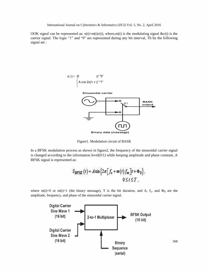
3. SYSTEM DESIGN We have an analog carrier signal & binary modulating signal .In modulation circuit the
corresponding modulation will be performed. In a BASK modulation process as shown in
figure1, the amplitude of the sinusoidal carrier signal is changed according to the message level
(0/1) while keeping the frequency and phase of carrier signal constant .The transmitted signal for
International Journal on Cybernetics & Informatics (IJCI) Vol. 5, No. 2, April 2016
368
OOK signal can be represented as: s(t)=m(t)c(t), where,m(t) is the modulating signal &c(t) is the
carrier signal. The logic “1” and “0” are represented during any bit interval, Tb by the following
signal set :
Figure1. Modulation circuit of BASK
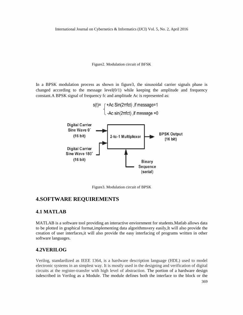
In a BFSK modulation process as shown in figure2, the frequency of the sinusoidal carrier signal
is changed according to the information level(0/1) while keeping amplitude and phase constant..A
BFSK signal is represented as:
where m(t)=0 or m(t)=1 (the binary message), T is the bit duration, and A, fc, and Φ0 are the
amplitude, frequency, and phase of the sinusoidal carrier signal.
International Journal on Cybernetics & Informatics (IJCI) Vol. 5, No. 2, April 2016
369
Figure2. Modulation circuit of BFSK
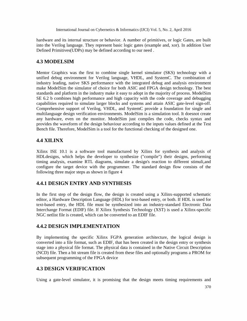
In a BPSK modulation process as shown in figure3, the sinusoidal carrier signals phase is
changed according to the message level(0/1) while keeping the amplitude and frequency
constant.A BPSK signal of frequency fc and amplitude Ac is represented as:
Figure3. Modulation circuit of BPSK
4.SOFTWARE REQUIREMENTS
4.1 MATLAB
MATLAB is a software tool providing an interactive enviornment for students.Matlab allows data
to be plotted in graphical format,implementing data algorithmsvery easily,It will also provide the
creation of user interfaces,it will also provide the easy interfacing of programs written in other
software languages.
4.2VERILOG Verilog, standardized as IEEE 1364, is a hardware description language (HDL) used to model
electronic systems in an simplest way. It is mostly used in the designing and verification of digital
circuits at the register-transfer with high level of abstraction. The portion of a hardware design
isdescribed in Verilog as a Module. The module defines both the interface to the block or the
International Journal on Cybernetics & Informatics (IJCI) Vol. 5, No. 2, April 2016
370
hardware and its internal structure or behavior. A number of primitives, or logic Gates, are built
into the Verilog language. They represent basic logic gates (example and, xor). In addition User
Defined Primitives(UDPs) may be defined according to our need .
4.3 MODELSIM Mentor Graphics was the first to combine single kernel simulator (SKS) technology with a
unified debug environment for Verilog language, VHDL, and SystemC. The combination of
industry leading, native SKS performance with the integrated debug and analysis environment
make ModelSim the simulator of choice for both ASIC and FPGA design technology. The best
standards and platform in the industry make it easy to adopt in the majority of process. ModelSim
SE 6.2 b combines high performance and high capacity with the code coverage and debugging
capabilities required to simulate larger blocks and systems and attain ASIC gate-level sign-off.
Comprehensive support of Verilog, VHDL, and SystemC provide a foundation for single and
multilanguage design verification environments. ModelSim is a simulation tool. It doesnot create
any hardware, even on the monitor. ModelSim just compiles the code, checks syntax and
provides the waveform of the design behaviour according to the inputs values defined at the Test
Bench file. Therefore, ModelSim is a tool for the functional checking of the designed one.
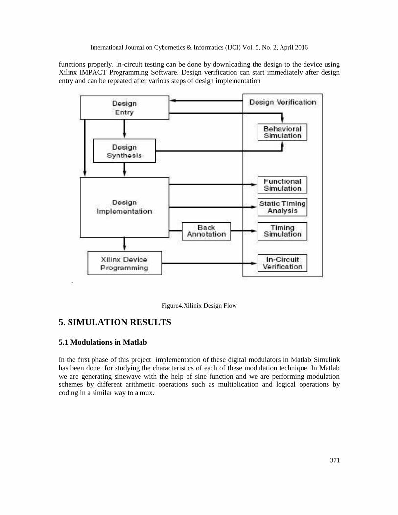
4.4 XILINX Xilinx ISE 10.1 is a software tool manufactured by Xilinx for synthesis and analysis of
HDLdesigns, which helps the developer to synthesize ("compile") their designs, performing
timing analysis, examine RTL diagrams, simulate a design's reaction to different stimuli,and
configure the target device with the programmer. The standard design flow consists of the
following three major steps as shown in figure 4
4.4.1 DESIGN ENTRY AND SYNTHESIS In the first step of the design flow, the design is created using a Xilinx-supported schematic
editor, a Hardware Description Language (HDL) for text-based entry, or both. If HDL is used for
text-based entry, the HDL file must be synthesized into an industry-standard Electronic Data
Interchange Format (EDIF) file. If Xilinx Synthesis Technology (XST) is used a Xilinx-specific
NGC netlist file is created, which can be converted to an EDIF file.
4.4.2 DESIGN IMPLEMENTATION By implementing the specific Xilinx FGPA generation architecture, the logical design is
converted into a file format, such as EDIF, that has been created in the design entry or synthesis
stage into a physical file format. The physical data is contained in the Native Circuit Description
(NCD) file. Then a bit stream file is created from these files and optionally programs a PROM for
subsequent programming of the FPGA device
4.3 DESIGN VERIFICATION Using a gate-level simulator, it is promising that the design meets timing requirements and
International Journal on Cybernetics & Informatics (IJCI) Vol. 5, No. 2, April 2016
371
functions properly. In-circuit testing can be done by downloading the design to the device using
Xilinx IMPACT Programming Software. Design verification can start immediately after design
entry and can be repeated after various steps of design implementation
.
Figure4.Xilinix Design Flow
5. SIMULATION RESULTS
5.1 Modulations in Matlab
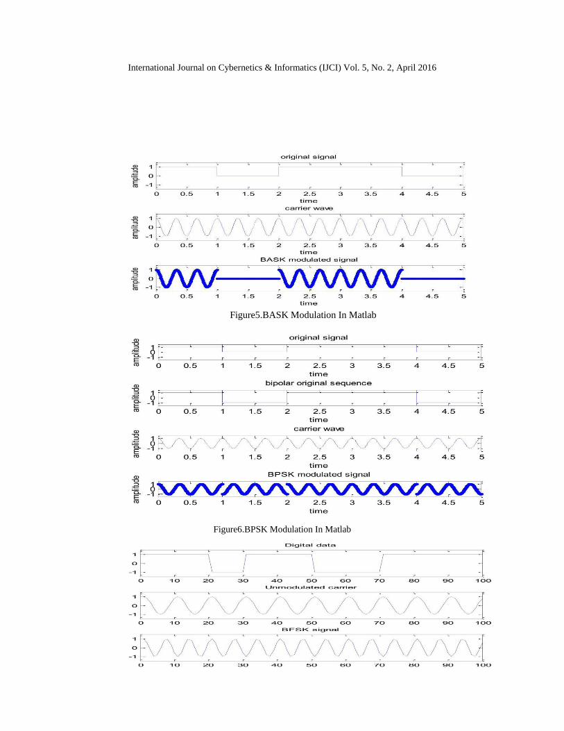
In the first phase of this project implementation of these digital modulators in Matlab Simulink
has been done for studying the characteristics of each of these modulation technique. In Matlab
we are generating sinewave with the help of sine function and we are performing modulation
schemes by different arithmetic operations such as multiplication and logical operations by
coding in a similar way to a mux.
International Journal on Cybernetics & Informatics (IJCI) Vol. 5, No. 2, April 2016
372
Figure5.BASK Modulation In Matlab
Figure6.BPSK Modulation In Matlab
International Journal on Cybernetics & Informatics (IJCI) Vol. 5, No. 2, April 2016
373
Figure7.BFSK Modulation In Matlab
In the BPSK signal for simplicity in doing modulation the binary input signal is converted to
bipolar signal.
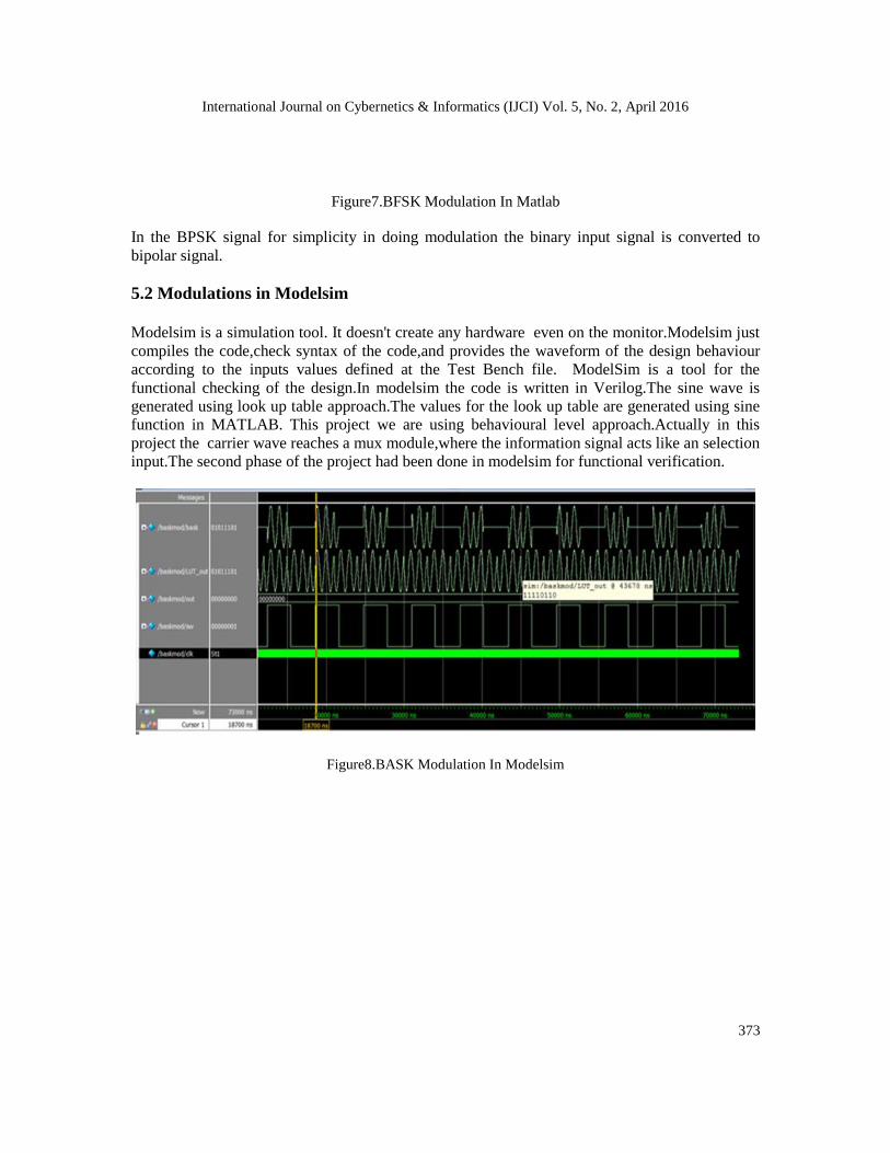
5.2 Modulations in Modelsim
Modelsim is a simulation tool. It doesn't create any hardware even on the monitor.Modelsim just
compiles the code,check syntax of the code,and provides the waveform of the design behaviour
according to the inputs values defined at the Test Bench file. ModelSim is a tool for the
functional checking of the design.In modelsim the code is written in Verilog.The sine wave is
generated using look up table approach.The values for the look up table are generated using sine
function in MATLAB. This project we are using behavioural level approach.Actually in this
project the carrier wave reaches a mux module,where the information signal acts like an selection
input.The second phase of the project had been done in modelsim for functional verification.
Figure8.BASK Modulation In Modelsim
International Journal on Cybernetics & Informatics (IJCI) Vol. 5, No. 2, April 2016
374
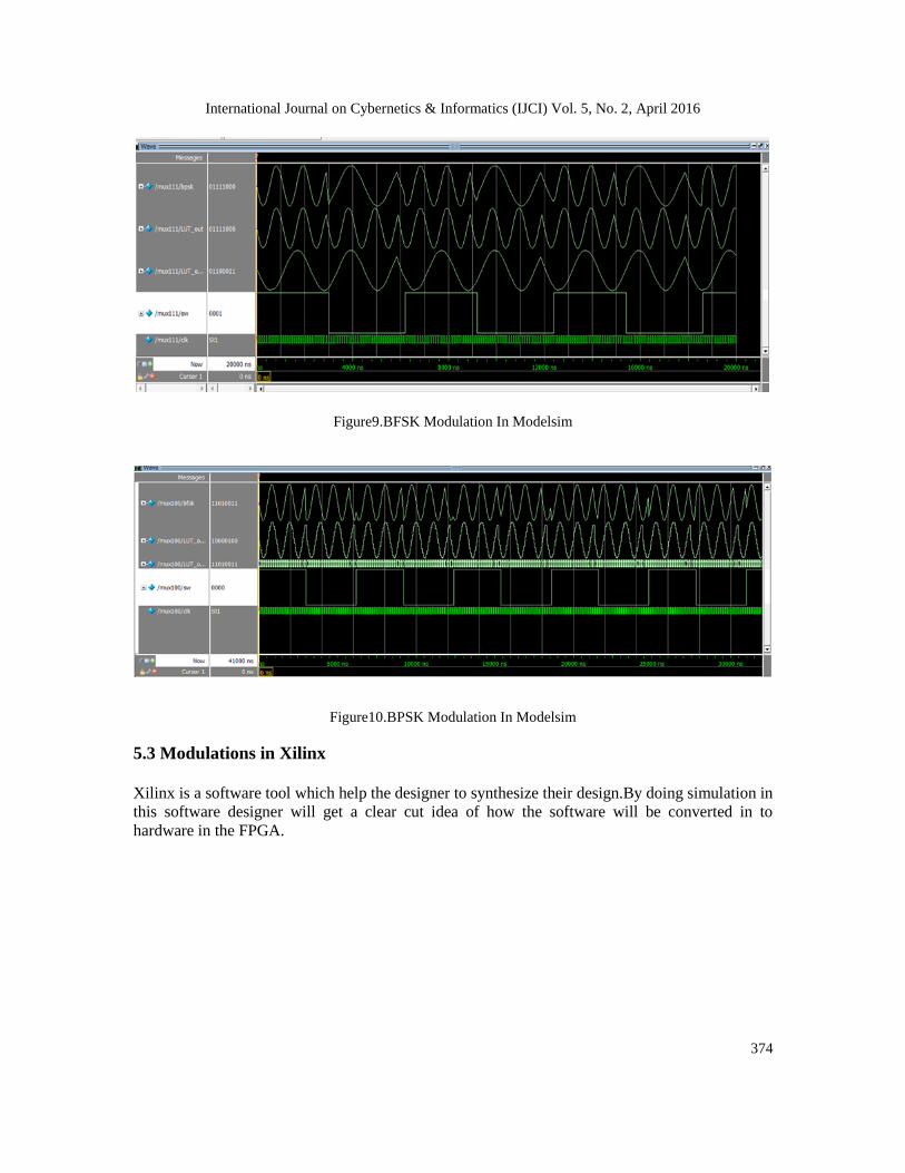
Figure9.BFSK Modulation In Modelsim
Figure10.BPSK Modulation In Modelsim
5.3 Modulations in Xilinx
Xilinx is a software tool which help the designer to synthesize their design.By doing simulation in
this software designer will get a clear cut idea of how the software will be converted in to
hardware in the FPGA.
International Journal on Cybernetics & Informatics (IJCI) Vol. 5, No. 2, April 2016
375
Figure 11:RTL View
The RTL view of modulation schemes is shown in figure11,here for BASK modulation the
Lookup table 2nd will be filled with zeroes, Look uptable1000 should be filled with normal sine
wave generating values, because for BASK modulation the output of the mux is switching
between carrier signal and zero depending on the information signal. For BPSK modulation
scheme both look up table are filled with same values for generating sine wave, but the BFSK
modulation is made possible switching the Look up table 2nd with a different time delay. In
BPSK, modulation both look up table have the same values, but the Look uptable2nd is switched
in such a way that the look up table value will be negative values.
5.CONCLUSION The project has been designed and developed successfully. Three modulations BASK,BPSK and
BFSK has been coded in MATLAB successfully. Programs for each building block of modulation
systems were written in Verilog. Mentor Graphics simulation tool ModelSim was used for writing
the code, simulating the programs and to test its behaviour. Xilinx Synthesis tool was used to
synthesize the modulation module by choosing Spartan 6 as the FPGA target device. The future
scope is creating a single IC which can perform BASK,BPSK,BFSK modulations.
International Journal on Cybernetics & Informatics (IJCI) Vol. 5, No. 2, April 2016
376
ACKNOWLEDGEMENT The satisfaction and euphoria of successful completion of any task would be incomplete without
the mention of the people who made it possible through their constant guidance and
encouragement. I would like to extend my heartfelt thanks to Asso. Prof. Deepa Elizabeth
George& Mr. George M Jacob of ECE DEPARTMENT TOCH Institute Of Science And
Technology, ARAKKUNNAM for the inspiration inculcated in us and for the apt guidance.
REFERENCE
[1] Ms. Neha P. Shrirao & Prof. Ajay P. Thakare“ Design of Digital Modulators: BASK, BPSK and BFSK
usingVHDL “International Journal of Advanced Research in Computer Science and Software
Engineering Volume 3, Issue 1, January 2013
[2] Mehmet Sonmez,Ayhan Akbal"FPGA Based BASK,BPSK,BFSK Modulators Using
VHDL:Design,Applications and Performance Comparison for Different Modulator Algorithm
,International Journal of Computer Applications ,Volume 42 ,March 2012
[3] C. Erdoğan, I. Myderrizi, and S. Minaei "FPGA Implementation of BASK-BFSK-BPSK
DigitalModulators"IEEE Antennas and Propagation Magazine, Vol. 54, No. 2, April 2012