134
Soft-Decision FEC Integrated Block v1.1 LogiCORE IP Product Guide Vivado Design Suite PG256 June 18, 2018

Soft-Decision FEC Integrated Block v1.1
LogiCORE IP Product Guide
Vivado Design Suite
PG256 June 18, 2018

SD-FEC Integrated Block v1.1 2PG256 June 18, 2018 www.xilinx.com
Table of ContentsIP Facts
Chapter 1: OverviewFeature Summary. . . . . . . . . . . . . . . . . . . . . . . . . . . . . . . . . . . . . . . . . . . . . . . . . . . . . . . . . . . . . . . . . . 5Applications . . . . . . . . . . . . . . . . . . . . . . . . . . . . . . . . . . . . . . . . . . . . . . . . . . . . . . . . . . . . . . . . . . . . . . 7Licensing and Ordering . . . . . . . . . . . . . . . . . . . . . . . . . . . . . . . . . . . . . . . . . . . . . . . . . . . . . . . . . . . . . 7
Chapter 2: Product SpecificationPort Descriptions . . . . . . . . . . . . . . . . . . . . . . . . . . . . . . . . . . . . . . . . . . . . . . . . . . . . . . . . . . . . . . . . . 11Modes of Operation. . . . . . . . . . . . . . . . . . . . . . . . . . . . . . . . . . . . . . . . . . . . . . . . . . . . . . . . . . . . . . . 19Data Interfaces . . . . . . . . . . . . . . . . . . . . . . . . . . . . . . . . . . . . . . . . . . . . . . . . . . . . . . . . . . . . . . . . . . . 20Standards . . . . . . . . . . . . . . . . . . . . . . . . . . . . . . . . . . . . . . . . . . . . . . . . . . . . . . . . . . . . . . . . . . . . . . . 32Performance. . . . . . . . . . . . . . . . . . . . . . . . . . . . . . . . . . . . . . . . . . . . . . . . . . . . . . . . . . . . . . . . . . . . . 32Register Space . . . . . . . . . . . . . . . . . . . . . . . . . . . . . . . . . . . . . . . . . . . . . . . . . . . . . . . . . . . . . . . . . . . 55
Chapter 3: Designing with the CoreClocking. . . . . . . . . . . . . . . . . . . . . . . . . . . . . . . . . . . . . . . . . . . . . . . . . . . . . . . . . . . . . . . . . . . . . . . . . 71Resets . . . . . . . . . . . . . . . . . . . . . . . . . . . . . . . . . . . . . . . . . . . . . . . . . . . . . . . . . . . . . . . . . . . . . . . . . . 71Interrupt . . . . . . . . . . . . . . . . . . . . . . . . . . . . . . . . . . . . . . . . . . . . . . . . . . . . . . . . . . . . . . . . . . . . . . . . 72Interfaces . . . . . . . . . . . . . . . . . . . . . . . . . . . . . . . . . . . . . . . . . . . . . . . . . . . . . . . . . . . . . . . . . . . . . . . 73LDPC Code Support . . . . . . . . . . . . . . . . . . . . . . . . . . . . . . . . . . . . . . . . . . . . . . . . . . . . . . . . . . . . . . . 74LDPC Code Memory Error Detection and Correction. . . . . . . . . . . . . . . . . . . . . . . . . . . . . . . . . . . . . 82
Chapter 4: Design Flow StepsCustomizing and Generating the Core . . . . . . . . . . . . . . . . . . . . . . . . . . . . . . . . . . . . . . . . . . . . . . . . 83Constraining the Core . . . . . . . . . . . . . . . . . . . . . . . . . . . . . . . . . . . . . . . . . . . . . . . . . . . . . . . . . . . . . 94Simulation . . . . . . . . . . . . . . . . . . . . . . . . . . . . . . . . . . . . . . . . . . . . . . . . . . . . . . . . . . . . . . . . . . . . . . 95Synthesis and Implementation . . . . . . . . . . . . . . . . . . . . . . . . . . . . . . . . . . . . . . . . . . . . . . . . . . . . . . 95
Chapter 5: C ModelUnpacking and Model Contents . . . . . . . . . . . . . . . . . . . . . . . . . . . . . . . . . . . . . . . . . . . . . . . . . . . . . 97Installation . . . . . . . . . . . . . . . . . . . . . . . . . . . . . . . . . . . . . . . . . . . . . . . . . . . . . . . . . . . . . . . . . . . . . . 99C Model Interface. . . . . . . . . . . . . . . . . . . . . . . . . . . . . . . . . . . . . . . . . . . . . . . . . . . . . . . . . . . . . . . . . 99MATLAB Interface . . . . . . . . . . . . . . . . . . . . . . . . . . . . . . . . . . . . . . . . . . . . . . . . . . . . . . . . . . . . . . . 105
Send Feedback
SD-FEC Integrated Block v1.1 3PG256 June 18, 2018 www.xilinx.com
Chapter 6: Example DesignSimulation-Only Example Design . . . . . . . . . . . . . . . . . . . . . . . . . . . . . . . . . . . . . . . . . . . . . . . . . . . 107Processor-Based Example Design . . . . . . . . . . . . . . . . . . . . . . . . . . . . . . . . . . . . . . . . . . . . . . . . . . . 108
Appendix A: Upgrading
Appendix B: DebuggingFinding Help on Xilinx.com . . . . . . . . . . . . . . . . . . . . . . . . . . . . . . . . . . . . . . . . . . . . . . . . . . . . . . . . 116Debug Tools . . . . . . . . . . . . . . . . . . . . . . . . . . . . . . . . . . . . . . . . . . . . . . . . . . . . . . . . . . . . . . . . . . . . 117Simulation Debug. . . . . . . . . . . . . . . . . . . . . . . . . . . . . . . . . . . . . . . . . . . . . . . . . . . . . . . . . . . . . . . . 118Hardware Debug . . . . . . . . . . . . . . . . . . . . . . . . . . . . . . . . . . . . . . . . . . . . . . . . . . . . . . . . . . . . . . . . 119Interface Debug . . . . . . . . . . . . . . . . . . . . . . . . . . . . . . . . . . . . . . . . . . . . . . . . . . . . . . . . . . . . . . . . . 119
Appendix C: SD-FEC Low-Level Bare-Metal DriverOverview . . . . . . . . . . . . . . . . . . . . . . . . . . . . . . . . . . . . . . . . . . . . . . . . . . . . . . . . . . . . . . . . . . . . . . 121Data Structures . . . . . . . . . . . . . . . . . . . . . . . . . . . . . . . . . . . . . . . . . . . . . . . . . . . . . . . . . . . . . . . . . 122User API . . . . . . . . . . . . . . . . . . . . . . . . . . . . . . . . . . . . . . . . . . . . . . . . . . . . . . . . . . . . . . . . . . . . . . . 124Interrupt Handling . . . . . . . . . . . . . . . . . . . . . . . . . . . . . . . . . . . . . . . . . . . . . . . . . . . . . . . . . . . . . . . 129Examples. . . . . . . . . . . . . . . . . . . . . . . . . . . . . . . . . . . . . . . . . . . . . . . . . . . . . . . . . . . . . . . . . . . . . . . 129
Appendix D: Additional Resources and Legal NoticesXilinx Resources . . . . . . . . . . . . . . . . . . . . . . . . . . . . . . . . . . . . . . . . . . . . . . . . . . . . . . . . . . . . . . . . . 132Documentation Navigator and Design Hubs . . . . . . . . . . . . . . . . . . . . . . . . . . . . . . . . . . . . . . . . . . 132References . . . . . . . . . . . . . . . . . . . . . . . . . . . . . . . . . . . . . . . . . . . . . . . . . . . . . . . . . . . . . . . . . . . . . 133Revision History . . . . . . . . . . . . . . . . . . . . . . . . . . . . . . . . . . . . . . . . . . . . . . . . . . . . . . . . . . . . . . . . . 134Please Read: Important Legal Notices . . . . . . . . . . . . . . . . . . . . . . . . . . . . . . . . . . . . . . . . . . . . . . . 134
Send Feedback

SD-FEC Integrated Block v1.1 4PG256 June 18, 2018 www.xilinx.com Product Specification
IntroductionThe Soft-Decision Forward Error Correction (SD-FEC) integrated block supports Low Density Parity Check (LDPC) decoding and encoding and Turbo code decoding. The LDPC codes used are highly configurable, and the specific code used can be specified on a codeword-by-codeword basis.
Features• Function configurable between either:
° LDPC decode or encode of a range of customer specified Quasi-cyclic (QC) codes, or
° Turbo decode of codes used by LTE [Ref 14]
• Peak throughput(1) of the order:
° 1.78 Gb/s Turbo decode @ 6 iterations
° 2.84 Gb/s for LDPC Decode @ 8 iterations
° 19.82 Gb/s for LDPC Encode
• Scalable implementation
° Multiple instantiations on a device (see Placement Location Guidelines for SD-FEC IP Core)
• High bandwidth AXI4-Stream interfaces
1. See performance in Table 2-22 for core clock frequency of 667 MHz. Throughput depends on the codes and how they are mixed and the actual clock frequency on the device See Clocking for further details.
IP Facts
LogiCORE™ IP Facts Table
Core SpecificsSupported Device Family(1) Zynq® UltraScale+™ RFSoC
Supported User Interfaces AXI4-Lite, AXI4-Stream
Resources Performance and Resource Utilization web page
Provided with CoreDesign Files -
Example Design IP Integrator Block Diagram
Test Bench Verilog
Constraints File Xilinx Design Constraints (XDC)
Simulation Model
System Verilog SecureIP model and C numericalmodel
Supported S/W Driver(2)
StandaloneLinux
Tested Design Flows(3)
Design Entry Vivado® Design Suite
Simulation For supported simulators, see theXilinx Design Tools: Release Notes Guide
Synthesis Vivado
SupportProvided by Xilinx at the Xilinx Support web page
Notes: 1. For a complete list of supported devices, see the Vivado IP
catalog.2. Stand-alone driver details can be found in the software
development kit (SDK) directory (<install_directory>/SDK/ <release>/data/embeddedsw/doc/xilinx_drivers.htm).
° Linux: Linux OS and driver support information is available from the Linux SD-FEC Driver page.
° Bare Metal: Bare-metal documentation is available in the SD-FEC Low-Level Bare-Metal Driver appendix.
3. For the supported versions of the tools, see theXilinx Design Tools: Release Notes Guide.
Send Feedback

SD-FEC Integrated Block v1.1 5PG256 June 18, 2018 www.xilinx.com
Chapter 1
OverviewForward Error Correction (FEC) codes such as Low Density Parity Check (LDPC) and Turbo codes provide a means to control errors in data transmissions over unreliable or noisy communication channels. The Soft-Decision FEC (SD-FEC) Integrated Block provides an optimized block for soft-decision decoding of these codes. Fixed Turbo codes, as used by LTE, are supported directly, whereas custom and standardized LDPC codes are supported through the ability to specify the parity check matrix through an AXI4-Lite bus or using the optional programmable logic (PL)-based support logic.
Feature SummaryThe SD-FEC core is a highly flexible soft-decision FEC decoder and LDPC encoder offering the following features:
LDPC Decoding/Encoding• Highly configurable codes
° A range of quasi-cyclic codes can be configured over an AXI4-Lite interface
° Code parameter memory can be shared across up to 128 codes
° Codes can be selected on a block-by-block basis
° Encoder can re-use suitable decoder codes
• Normalized min-sum decoding algorithm
° Normalization factor programmable (from 0.0625 to 1 in steps of 0.0625) for layers
• Number of iterations between 1 and 63
° Specified for each block using the AXI4-Stream control interface
• Early termination
° Specified for each block to be none, one, or both of the following:
- Parity check passes
- No change in hard information or parity bits since last iteration
Send Feedback

SD-FEC Integrated Block v1.1 6PG256 June 18, 2018 www.xilinx.com
Chapter 1: Overview
• Soft or hard outputs
° Specified for each block to include information and optional parity
° 6-bit soft log-likelihood ratio (LLR) input (8-bit interface, 2 fractional bits, with external saturation before input to symmetric range -7.75 to +7.75 assumed) and 8-bit output
• In- or out-of-order execution of blocks, with user specified ID field to identify blocks
• Encoder and decoder variants, with optional support for improved throughput when sub-matrix size is small
• Optional final parity check to update parity pass/fail for final output
• Optional initialization of codes from device configuration, avoiding download using AXI4-Lite interface
° Support logic for 5G NR provides code generation and download to SD-FEC internal memory during run-time and initialization
° Support logic for non-5G provides code generation and download to SD-FEC internal memory during initialization
Turbo Decoding• Max, Max Scale (scale factor is programmable as a multiple of 0.0625) or Max Star
• Number of iterations between 1 and 63
° Specified for each block using the AXI4-Stream control interface
• Early termination
° Specified for each block to be none, one, or both of the following:
- No change in hard decision since last iteration
- CRC pass
• Soft or hard outputs
° Specified for each block to include systematic and optionally parity 0 and parity 1
° 8-bit soft LLR on input and output (8-bit interface, 2 fractional bits, with external saturation before input to symmetric range -31.75 to +31.75 is assumed)
Interfaces• Separate clocks on each interface to ease integration
• Wide data interfaces on input and output with configurable support for 1, 2 or 4 lanes
• Ability to specify number of inputs and outputs on each lane on either a block-by-block basis, or transfer basis
Send Feedback

SD-FEC Integrated Block v1.1 7PG256 June 18, 2018 www.xilinx.com
Chapter 1: Overview
• Separate inputs to specify control parameters and receive status output on a block-by-block basis
ApplicationsThe SD-FEC core is intended for use in applications requiring LTE Turbo decoding or LDPC encode/decode, such as 5G wireless (3GPP TS 38.212 V15.0.0 Multiplexing and channel coding (Release 15) [Ref 11]), backhaul and DOCSIS 3.1 cable modems (Data-Over-Cable Service Interface Specifications [Ref 12]).
Licensing and OrderingThis Xilinx LogiCORE™ IP module is provided at no additional cost with the Xilinx Vivado Design Suite under the terms of the Xilinx End User License. Registration is required to obtain the license. Information about this and other Xilinx LogiCORE IP modules is available at the Xilinx Intellectual Property page. For information about pricing and availability of other Xilinx LogiCORE IP modules and tools, contact your local Xilinx sales representative.
France Telecom, for itself and certain other parties, claims certain intellectual property rights covering Turbo Codes technology, and has decided to license these rights under a licensing program called the Turbo Codes Licensing Program. Supply of this IP core does not convey a license nor imply any right to use any Turbo Codes patents owned by France Telecom, TDF or GET. Contact France Telecom for information about its Turbo Codes Licensing Program at the following address:
France Telecom R&D,VAT/TURBOCODES,38, rue du Général Leclerc,92794 Issy Moulineaux,Cedex 9,France.
Send Feedback

SD-FEC Integrated Block v1.1 8PG256 June 18, 2018 www.xilinx.com
Chapter 2: Product Specification
Chapter 2
Product SpecificationA block diagram of the SD-FEC block is shown in Figure 2-1, which includes the high speed clock (667 MHz) domain and the Clock Domain Crossing (CDC) blocks. Optional Support logic is provided around the SD-FEC block to configure it; for 5G NR the optional logic provides support for both initialization and run-time configuration and for non-5G NR it provides support for initialization only. The optional support logic is generated using the Vivado® Integrated Design Environment. The optional support logic and SD-FEC block are referred to as the SD-FEC core.X-Ref Target - Figure 2-1
Figure 2-1: SD-FEC Cores Interfaces
Send Feedback
SD-FEC Integrated Block v1.1 9PG256 June 18, 2018 www.xilinx.com
Chapter 2: Product Specification
The SD-FEC core provides:
• Turbo Decode for LTE
• LDPC Decode for a wide range of codes defined by the user
• LDPC Encode for a wide range of codes defined by the user
The core uses AXI4 interfaces. A single AXI4-Lite memory mapped bus is used for parameters, such as LDPC code definitions, that persist for more than one block, and AXI4-Stream interfaces are used to provide data on a sample-by-sample basis (for example, DIN), or block-by-block basis (for example, CTRL). These interfaces provide handshake signals in addition to data. Further details are given in AXI4-Stream Interface. Data input and output buffers provide some scope to overlap input and output with encoder/decoder operation.
For Turbo Decode, the SD-FEC core can be configured in two modes, initialized and run-time configured. In initialized mode, the support logic initializes the SD-FEC block at startup based on the user-selectable parameters in the Vivado IDE. In run-time configured mode, the configuration is set using the AXI4-Lite interface. In both cases, AXI4-Lite interface is exposed.
For LDPC Encode or Decode, the core can be configured in 5G and non-5G NR modes. In 5G mode, the 5G support logic downloads code definitions to the SD-FEC IP core as soon as a code is available on the control interface. This avoids having to generate any 5G code or having to write to the core through the AXI4-Lite interface. The non-5G mode is further classified into two sub-types, initialized non-5G and run-time configured non-5G. In initialized non-5G, the core is initialized with user-selectable codes by the non-5G support logic. In the non-5G run-time configured case, use the AXI4-Lite interface to write code definitions to the core.
In 5G mode, the 5G support logic extends the width of the code definition bus of both the CTRL and STATUS interfaces to 40 bits.
Each block is input through the data input interface (DIN) over a number of cycles. The amount of data transferred on each cycle is set by a separate data stream (DIN_WORDS) where a value is given per transaction on DIN. If this does not need to be changed, then there is an option to tie this off in the Vivado IDE. The output is generated in a similar way on the DOUT output stream, and similarly, the amount of data transferred is specified on the input data stream, DOUT_WORDS. If the number of words is fixed, then the core optional support logic ties this input off.
For each data block, a single input is required on the control (CTRL) input stream, specifying key block specific parameters, such as block size. One control word (transaction) is required for each data block, and data input stalls until the relevant control word is available. When decoded (or encoded in the case of LDPC), the output data is provided on DOUT along with a status word on the status (STATUS) output interface.
Send Feedback
SD-FEC Integrated Block v1.1 10PG256 June 18, 2018 www.xilinx.com
Chapter 2: Product Specification
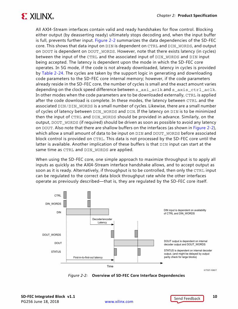
All AXI4-Stream interfaces contain valid and ready handshakes for flow control. Blocking either output (by deasserting ready) ultimately stops decoding and, when the input buffer is full, prevents further input. Figure 2-2 summarizes the data dependencies of the SD-FEC core. This shows that data input on DIN is dependent on CTRL and DIN_WORDS, and output on DOUT is dependent on DOUT_WORDS. However, note that there exists latency (in cycles) between the input of the CTRL and the associated input of DIN_WORDS and DIN input being accepted. The latency is dependent upon the mode in which the SD-FEC core operates. In 5G mode, if the code is not already downloaded, latency in cycles is provided by Table 2-24. The cycles are taken by the support logic in generating and downloading code parameters to the SD-FEC core internal memory; however, if the code parameters already reside in the SD-FEC core, the number of cycles is small and the exact amount varies depending on the clock speed difference between s_axi_aclk and s_axis_ctrl_aclk. In other modes when the code parameters are to be downloaded externally, CTRL is applied after the code download is complete. In these modes, the latency between CTRL and the associated DIN/DIN_WORDS is a small number of cycles. Likewise, there are a small number of cycles of latency between DIN_WORDS and DIN. If the latency on DIN is to be minimized then the input of CTRL and DIN_WORDS should be provided in advance. Similarly, on the output, DOUT_WORDS (if required) should be driven as soon as possible to avoid any latency on DOUT. Also note that there are shallow buffers on the interfaces (as shown in Figure 2-2), which allow a small amount of data to be input on DIN and DOUT_WORDS before associated block control is provided on CTRL. This data is not processed by the SD-FEC core until the latter is available. Another implication of these buffers is that DIN input can start at the same time as CTRL and DIN_WORDS are applied.
When using the SD-FEC core, one simple approach to maximize throughput is to apply all inputs as quickly as the AXI4-Stream interface handshake allows, and to accept output as soon as it is ready. Alternatively, if throughput is to be controlled, then only the CTRL input can be regulated to the correct data block throughput rate while the other interfaces operate as previously described—that is, they are regulated by the SD-FEC core itself.
X-Ref Target - Figure 2-2
Figure 2-2: Overview of SD-FEC Core Interface Dependencies
CTRL
DIN
DIN_WORDS
STATUS
DOUT
DOUT_WORDS
DIN input is dependent on availability of CTRL and DIN_WORDS
DOUT output is dependent on internal decoder output and DOUT_WORDS
STATUS is dependent on internal decoder output, (and might be delayed by output parity check for large blocks)
Time
Decoder/encoderLatency
First-in-to-first-out latency
Send Feedback
SD-FEC Integrated Block v1.1 11PG256 June 18, 2018 www.xilinx.com
Chapter 2: Product Specification
As shown in Figure 2-1, the internals of the SD-FEC core operate off a high speed clock, whereas the interfaces have their own clocks for ease of integration. Clock Domain Crossing (CDC) is provided on all interfaces and the data interfaces include width conversion to maintain high bandwidth with lower interface clock frequency. Specifically, the high speed clock domain has a 128-bit data interface capable of carrying up to 16 8-bit LLRs per clock cycle of the core, but the block has a 512-bit data interface, which allows up to four 128-bit samples to be time division multiplexed onto the core interface. This number can be configured to 1, 2 or 4 (using the AXI4-Lite interface), and if configured to 4, for example, it allows the interface clock rate to be reduced by a factor of four relative to the core clock while maintaining maximum bandwidth.
Note: DIN_WORDS and DOUT_WORDS have a more advanced mode of operation, where the number of elements is specified for each transfer over DIN or DOUT. This is supported by width conversion.
Port DescriptionsTable 2-1 shows the core pinout.
Table 2-1: Core Pinout
Signal I/O Width Clock Domain Description
reset_n Input 1 NONE Master asynchronous reset
core_clk Input 1 core_clkMain processing clock for processing core
interrupt(1) Output 1 s_axi_aclk
Indicates error conditions. Behavior controlled by interrupt control registers.
Send Feedback

SD-FEC Integrated Block v1.1 12PG256 June 18, 2018 www.xilinx.com
Chapter 2: Product Specification
s_axi_aclk Input 1 s_axi_aclk
Parameter Bus: AXI4-Lite memory-mapped Slave interface(2)
s_axi_awaddr Input 18 s_axi_aclk
s_axi_awvalid Input 1 s_axi_aclk
s_axi_awready Output 1 s_axi_aclk
s_axi_wdata Input 32 s_axi_aclk
s_axi_wvalid Input 1 s_axi_aclk
s_axi_wready Output 1 s_axi_aclk
s_axi_bready Input 1 s_axi_aclk
s_axi_bvalid Output 1 s_axi_aclk
s_axi_araddr Input 18 s_axi_aclk
s_axi_arvalid Input 1 s_axi_aclk
s_axi_arready Output 1 s_axi_aclk
s_axi_rready Input 1 s_axi_aclk
s_axi_rdata Output 32 s_axi_aclk
s_axi_rvalid Output 1 s_axi_aclk
s_axis_din_words_aclk Input 1 s_axis_din_words_aclk
Controls number of words on Data Input Bus: AXI4-Stream Slave interface(5)
s_axis_din_words_tvalid Input 1 s_axis_din_words_aclk
s_axis_din_words_tready Output 1 s_axis_din_words_aclk
s_axis_din_words_tlast Input 1 s_axis_din_words_aclk
s_axis_din_words_tdata Input 8*(LANE_NUM_IN)(3)(4) s_axis_din_words_aclk
s_axis_ctrl_aclk Input 1 s_axis_ctrl_aclkControl Input Bus: AXI4-Stream Slave interface
s_axis_ctrl_tvalid Input 1 s_axis_ctrl_aclk
s_axis_ctrl_tready Output 1 s_axis_ctrl_aclk
s_axis_ctrl_tdata Input 32/40(6) s_axis_ctrl_aclk
s_axis_din_aclk Input 1 s_axis_din_aclk
Data Input Bus: AXI4-Stream Slave interface
s_axis_din_tvalid Input 1 s_axis_din_aclk
s_axis_din_tready Output 1 s_axis_din_aclk
s_axis_din_tlast Input 1 s_axis_din_aclk
s_axis_din_tdata Input 128*(LANE_NUM_IN)(4) s_axis_din_aclk
m_axis_status_aclk Input 1 m_axis_status_aclkStatus Output Bus: AXI4- Stream Master interface
m_axis_status_tvalid Output 1 m_axis_status_aclk
m_axis_status_tready Input 1 m_axis_status_aclk
m_axis_status_tdata Output 32/40 m_axis_status_aclk
Table 2-1: Core Pinout (Cont’d)
Signal I/O Width Clock Domain Description
Send Feedback

SD-FEC Integrated Block v1.1 13PG256 June 18, 2018 www.xilinx.com
Chapter 2: Product Specification
Parameter BusThe AXI4-Lite parameter bus allows two outstanding transactions on the write interface, and one outstanding transaction on the read interface. The higher number of outstanding transactions on the write interface improves the write download throughput, allowing an LDPC code to be updated more quickly.
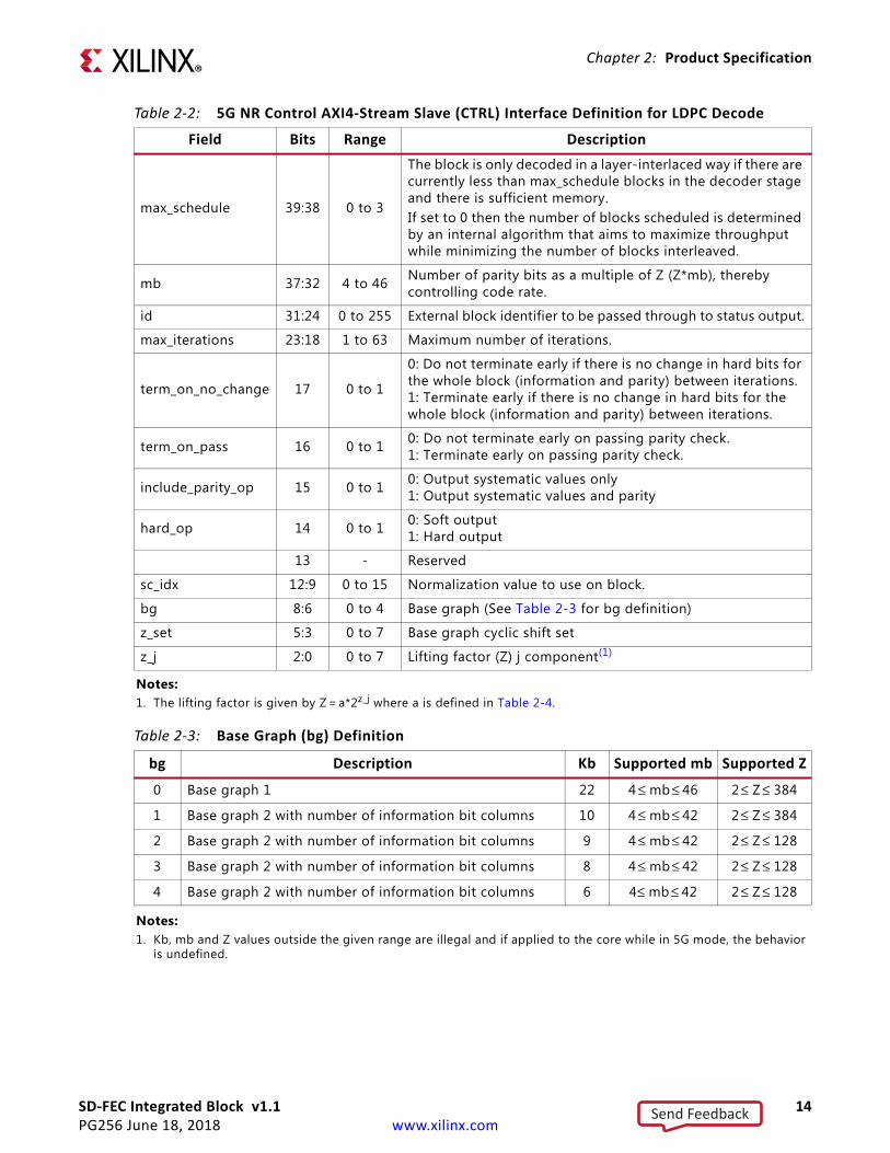
Control AXI4-Stream SlaveThe AXI4-Stream control (CTRL) input provides information specific to each block. Its definition depends on whether 5G NR standard support is selected in the Vivado® IDE.
5G NR Standard
When the 5G NR standard is supported the control interface is 40 bits with the fields shown in Table 2-2 and Table 2-5 for decode and encode respectively.
s_axis_dout_words_aclk Input 1 s_axis_dout_words_aclk
Controls number of words on Data Output Bus: AXI4-Stream Slave interface(7)
s_axis_dout_words_tvalid Input 1 s_axis_dout_words_aclk
s_axis_dout_words_tready Output 1 s_axis_dout_words_aclk
s_axis_dout_words_tlast Input 1 s_axis_dout_words_aclk
s_axis_dout_words_tdata Input 8*(LANE_NUM_OUT)(3)(4) s_axis_dout_words_aclk
m_axis_dout_aclk Input 1 m_axis_dout_aclk
Data Output Bus: AXI4-Stream Master interface
m_axis_dout_tvalid Output 1 m_axis_dout_aclk
m_axis_dout_tready Input 1 m_axis_dout_aclk
m_axis_dout_tlast Output 1 m_axis_dout_aclk
m_axis_dout_tdata Output 128*(LANE_NUM_OUT)(4) m_axis_dout_aclk
Notes: 1. Interrupt pin is present if Parameter_Interface is not Initialized or any interrupt source is enabled.2. AXI4-Lite interface is present when Parameter_Interface is not Initialized.3. Width is 8 bits when word configuration is Per Block.4. LANE_NUM_IN and LANE_NUM_OUT are the number of lanes configured using AXIS_WIDTH.DIN and
AXIS_WIDTH.DOUT respectively.5. Ports associated with DIN_WORDS interface are present if DIN_Interface is set to Unconfigured, or DIN_Interface is
set to Pre-Configured and DIN_Words_Configuration is set to Per_Block or Per_Transaction (that is, the interface is not Fixed).
6. 40 bits if Standard is set to 5G, otherwise 32 bits.7. Ports associated with DOUT_WORDS interface are present if DOUT_Interface is set to Unconfigured, or
DOUT_Interface is set to Pre-Configured and DOUT_Words_Configuration is set to Per_Block or Per_Transaction (that is, the interface is not Fixed).
Table 2-1: Core Pinout (Cont’d)
Signal I/O Width Clock Domain Description
Send Feedback
SD-FEC Integrated Block v1.1 14PG256 June 18, 2018 www.xilinx.com
Chapter 2: Product Specification
Table 2-2: 5G NR Control AXI4-Stream Slave (CTRL) Interface Definition for LDPC Decode
Field Bits Range Description
max_schedule 39:38 0 to 3
The block is only decoded in a layer-interlaced way if there are currently less than max_schedule blocks in the decoder stage and there is sufficient memory.If set to 0 then the number of blocks scheduled is determined by an internal algorithm that aims to maximize throughput while minimizing the number of blocks interleaved.
mb 37:32 4 to 46 Number of parity bits as a multiple of Z (Z*mb), thereby controlling code rate.
id 31:24 0 to 255 External block identifier to be passed through to status output.
max_iterations 23:18 1 to 63 Maximum number of iterations.
term_on_no_change 17 0 to 1
0: Do not terminate early if there is no change in hard bits for the whole block (information and parity) between iterations.1: Terminate early if there is no change in hard bits for the whole block (information and parity) between iterations.
term_on_pass 16 0 to 1 0: Do not terminate early on passing parity check.1: Terminate early on passing parity check.
include_parity_op 15 0 to 1 0: Output systematic values only1: Output systematic values and parity
hard_op 14 0 to 1 0: Soft output1: Hard output
13 - Reserved
sc_idx 12:9 0 to 15 Normalization value to use on block.
bg 8:6 0 to 4 Base graph (See Table 2-3 for bg definition)
z_set 5:3 0 to 7 Base graph cyclic shift set
z_j 2:0 0 to 7 Lifting factor (Z) j component(1)
Notes: 1. The lifting factor is given by Z = a*2z_j where a is defined in Table 2-4.
Table 2-3: Base Graph (bg) Definition
bg Description Kb Supported mb Supported Z
0 Base graph 1 22 4 ≤ mb ≤ 46 2 ≤ Z ≤ 384
1 Base graph 2 with number of information bit columns 10 4 ≤ mb ≤ 42 2 ≤ Z ≤ 384
2 Base graph 2 with number of information bit columns 9 4 ≤ mb ≤ 42 2 ≤ Z ≤ 128
3 Base graph 2 with number of information bit columns 8 4 ≤ mb ≤ 42 2 ≤ Z ≤ 128
4 Base graph 2 with number of information bit columns 6 4≤ mb ≤ 42 2 ≤ Z ≤ 128
Notes: 1. Kb, mb and Z values outside the given range are illegal and if applied to the core while in 5G mode, the behavior
is undefined.
Send Feedback

SD-FEC Integrated Block v1.1 15PG256 June 18, 2018 www.xilinx.com
Chapter 2: Product Specification
Non-5G NR Standards
When the supported standard is not 5G NR the control interface is 32 bits with the fields shown in Table 2-6 and Table 2-7 for decode and encode respectively.
Table 2-4: Lifting Factor Component (a) Definition
z_set (= Set Index iLS)(1) a
0 2
1 3
2 5
3 7
4 9
5 11
6 13
7 15
Notes: 1. As defined in 5G NR standard.
Table 2-5: 5G NR Control AXI4-Stream Slave (CTRL) Interface Definition for LDPC Encode
Field Bits Range Description
max_schedule 39:38 0 to 3
The block is only encoded in a layer-interlaced way if there are currently less than max_schedule blocks in the encoder stage and there is sufficient memory.If set to 0 then the maximum number of blocks interlaced is 4, subject to there being sufficient memory.
mb 37:32 4 to 46 Number of parity bits as a multiple of Z (Z*mb), thereby controlling code rate.
id 31:24 0 to 255 External block identifier to be passed through to status output.
23:9 - Reserved
bg 8:6 0 to 4 Base graph (See Table 2-3 for bg definition)
z_set 5:3 0 to 7 Base graph cyclic shift set
z_j 2:0 0 to 7 Lifting factor (Z) j component
Table 2-6: Control AXI4-Stream Slave (CTRL) Interface Definition for LDPC Decode
Field Bits Range Descriptionid 31:24 0 to 255 External block identifier to be passed through to status output
max_iterations 23:18 1 to 63 Maximum number of iterations
term_on_no_change 17 0 or 1
0: Do not terminate early if there is no change in hard bits for the whole block (information and parity) between iterations.1: Terminate early if there is no change in hard bits for the whole block (information and parity) between iterations.
Send Feedback

SD-FEC Integrated Block v1.1 16PG256 June 18, 2018 www.xilinx.com
Chapter 2: Product Specification
term_on_pass 16 0 or 1 0: Do not terminate early on passing parity check.1: Terminate early on passing parity check.
include_parity_op 15 0 to 1 0: Output systematic values only.1: Output systematic values and parity.
hard_op 14 0 to 1 0: Soft output1: Hard output
13:7 - Reserved
code 6:0 0 to 127 Code number (CODE) used to specify which set of LDPC code parameters are to be used on the block.
Table 2-7: Control AXI4-Stream Slave (CTRL) Interface Definition for LDPC Encode
Field Bits Range Descriptionid 31:24 0 to 255 External block identifier to be passed through to status output.
23:7 - Reserved
code 6:0 0 to 127 Code number (CODE) used to specify which set of LDPC code parameters are to be used on the block.
Table 2-8: Control AXI4-Stream Slave (CTRL) Interface Definition for Turbo Decode
Field Bits Range Description
id 31:24 0 to 255 External block identifier to be passed through to status output
max_iterations 23:18 1 to 63 Maximum number of iterations
term_on_no_change 17 0 or 1
0: Do not terminate early if there is no change in the hard systematic bits for the block between iterations.1: Terminate early if there is no change in the hard systematic bits between iterations.
term_on_pass 16 0 or 10: Do not terminate early if CRC passes1: Terminate early if CRC passes
include_parity_op 15 0 to 10: Output systematic values only1: Output systematic values and parity
hard_op 14 0 to 10: Soft output1: Hard output
crc_type 13 0 to 1
0: CRC24B1: CRC24AThese CRC types are defined in 3GPP TS 38.212 V15.0.0 Multiplexing and channel coding [Ref 11].
code_block_size 12:0 40 to 6144 Turbo code block size (K). Encoded block size N=3*K+12.
Table 2-6: Control AXI4-Stream Slave (CTRL) Interface Definition for LDPC Decode (Cont’d)
Field Bits Range Description
Send Feedback

SD-FEC Integrated Block v1.1 17PG256 June 18, 2018 www.xilinx.com
Chapter 2: Product Specification
Status AXI4-Stream MasterThe AXI4-Stream status (STATUS) output provides information specific to each block. Its definition depends on whether 5G NR standard support is selected in the Vivado IDE.
5G NR Standard
When the 5G NR standard is supported the status interface is 40 bits with the fields shown in Table 2-9 and Table 2-10 for decode and encode respectively.
Table 2-9: 5G NR Status AXI4-Stream Master (STATUS) Interface Definition for LDPC Decode
Field Bits Range Description
39:38 - Reserved
mb 37:32 4 to 46 Number of parity bits as a multiple of Z (Z*mb), thereby controlling code rate.
id 31:24 0 to 255 External block identifier supplied through control input
dec_iter 23:18 1 to 63 Number of iterations taken to decode output (either successfully or unsuccessfully)
term_no_change 17 0 to 1
0: Did not terminate early due to no change in hard bits for the whole block (information and parity) between iterations.1: Terminated early as no change in hard bits for the whole block (information and parity) between iterations.
term_pass 16 0 to 10: Did not terminate due to passing parity check1: Terminated early due to passing parity check
pass 15 0 to 10: Parity check did not pass1: Parity check passed
hard_op 14 0 to 10: Soft output1: Hard output
op 13 0 Decode operation (fixed value)
12:9 - Reserved
bg 8:6 0 to 4 Base graph (See Table 2-3 for bg definition)
z_set 5:3 0 to 7 Base graph cyclic shift set
z_j 2:0 0 to 7 Lifting factor (Z) j component(1)
Notes: 1. The lifting factor is given by Z = a*2z_j where a is defined in Table 2-4.
Send Feedback

SD-FEC Integrated Block v1.1 18PG256 June 18, 2018 www.xilinx.com
Chapter 2: Product Specification
Non-5G NR Standards
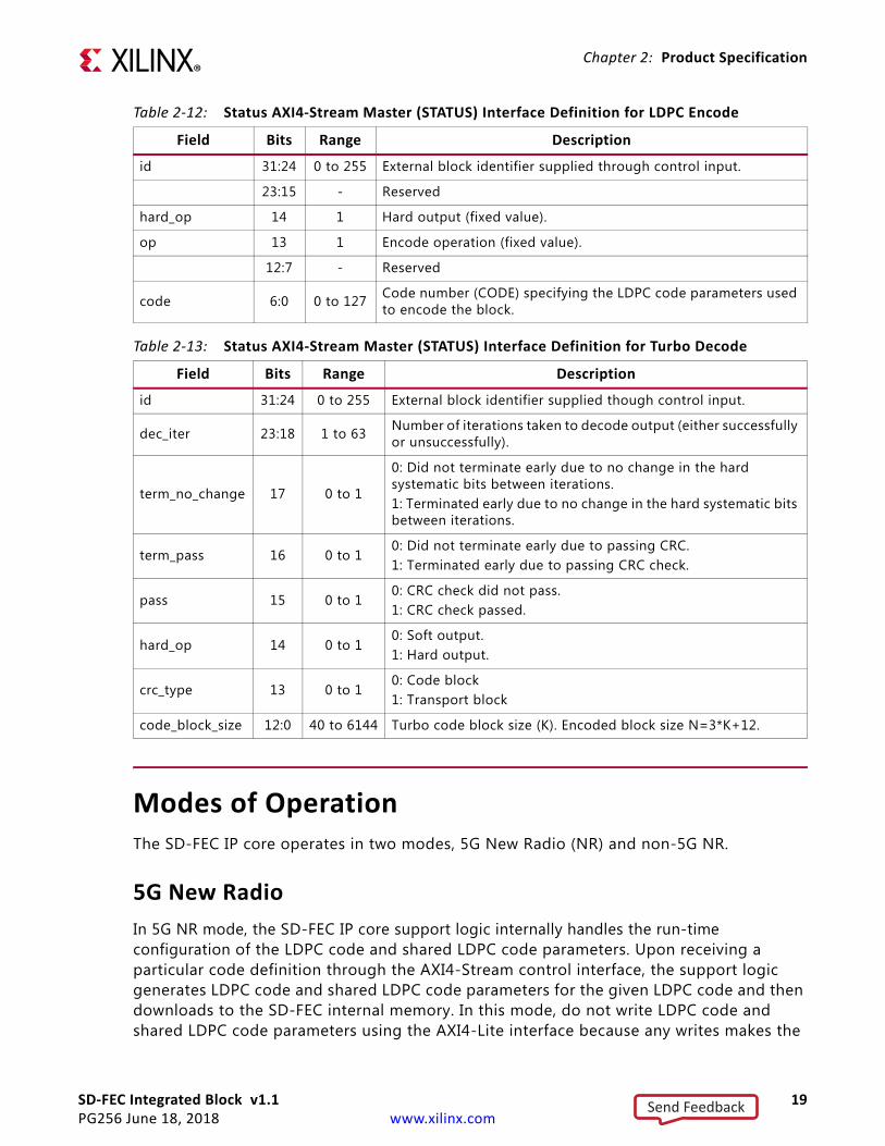
When the supported standard is not 5G NR the status interface is 32 bits with the fields shown in Table 2-11 and Table 2-12 for decode and encode respectively.
Table 2-10: 5G NR Status AXI4-Stream Master (STATUS) Interface Definition for LDPC Encode
Field Bits Range Description
39:38 - Reserved
mb 37:32 4 to 46 Number of parity bits as a multiple of Z (Z*mb), thereby controlling code rate
id 31:24 0 to 255 External block identifier supplied through control input
23:15 - Reserved
hard_op 14 1 Hard output (fixed value)
op 13 1 Encode operation (fixed value)
12:9 - Reserved
bg 8:6 0 to 4 Base graph (See Table 2-3 for bg definition)
z_set 5:3 0 to 7 Base graph cyclic shift set
z_j 2:0 0 to 7 Lifting factor (Z) j component
Table 2-11: Status AXI4-Stream Master (STATUS) Interface Definition for LDPC Decode
Field Bits Range Description
id 31:24 0 to 255 External block identifier supplied through control input.
dec_iter 23:18 1 to 63 Number of iterations taken to decode output (either successfully or unsuccessfully)
term_no_change 17 0 to 1
0: Did not terminate early due to no change in hard bits for the whole block (information and parity) between iterations.1: Terminated early as no change in hard bits for the whole block (information and parity) between iterations.
term_pass 16 0 to 10: Did not terminate due to passing parity check.1: Terminated early due to passing parity check.
pass 15 0 to 10: Parity check did not pass.1: Parity check passed.
hard_op 14 0 to 10: Soft output1: Hard output
op 13 0 Decode operation (fixed value)
12:7 - Reserved
code 6:0 0 to 127 Code number (CODE) specifying the LDPC code parameters used to decode the block
Send Feedback
SD-FEC Integrated Block v1.1 19PG256 June 18, 2018 www.xilinx.com
Chapter 2: Product Specification
Modes of OperationThe SD-FEC IP core operates in two modes, 5G New Radio (NR) and non-5G NR.
5G New RadioIn 5G NR mode, the SD-FEC IP core support logic internally handles the run-time configuration of the LDPC code and shared LDPC code parameters. Upon receiving a particular code definition through the AXI4-Stream control interface, the support logic generates LDPC code and shared LDPC code parameters for the given LDPC code and then downloads to the SD-FEC internal memory. In this mode, do not write LDPC code and shared LDPC code parameters using the AXI4-Lite interface because any writes makes the
Table 2-12: Status AXI4-Stream Master (STATUS) Interface Definition for LDPC Encode
Field Bits Range Description
id 31:24 0 to 255 External block identifier supplied through control input.
23:15 - Reserved
hard_op 14 1 Hard output (fixed value).
op 13 1 Encode operation (fixed value).
12:7 - Reserved
code 6:0 0 to 127 Code number (CODE) specifying the LDPC code parameters used to encode the block.
Table 2-13: Status AXI4-Stream Master (STATUS) Interface Definition for Turbo Decode
Field Bits Range Description
id 31:24 0 to 255 External block identifier supplied though control input.
dec_iter 23:18 1 to 63 Number of iterations taken to decode output (either successfully or unsuccessfully).
term_no_change 17 0 to 1
0: Did not terminate early due to no change in the hard systematic bits between iterations.1: Terminated early due to no change in the hard systematic bits between iterations.
term_pass 16 0 to 10: Did not terminate early due to passing CRC.1: Terminated early due to passing CRC check.
pass 15 0 to 10: CRC check did not pass.1: CRC check passed.
hard_op 14 0 to 10: Soft output.1: Hard output.
crc_type 13 0 to 10: Code block1: Transport block
code_block_size 12:0 40 to 6144 Turbo code block size (K). Encoded block size N=3*K+12.
Send Feedback

SD-FEC Integrated Block v1.1 20PG256 June 18, 2018 www.xilinx.com
Chapter 2: Product Specification
behavior unpredictable. This mode also assumes CTRL and STATUS are enabled in the AXIS_ENABLE register. This register must be written with CTRL (bit-0) and STATUS (bit-3) always set to 1 (enabled). Writing any other value to the CTRL (bit-0) makes the behavior unpredictable.
Non-5G NRThis is further classified into initialized and run-time configured modes.
Run-time Configured Non-5G NR Mode
In this mode the core is configured at run-time using the AXI4-Lite (S_AXI) and the AXI4-Stream control interface (S_AXIS_CTRL) for either Turbo decode or LDPC encode or decode.
Initialized Non-5G NR Mode
In this mode the core support logic generates initialization and configuration parameters at start up from the options set in the Vivado IDE for either Turbo decode or LDPC encode or decode. In this mode and for LDPC, do not write LDPC code and shared LDPC code parameters using the AXI4-Lite interface because any write can overwrite the initialized codes and make the behavior unpredictable.
Data Interfaces
Soft Value LLR RepresentationFor both Turbo and LDPC decode, the soft value log-likelihood ratio is defined as:
Equation 2-1
As a consequence, negative LLR values are interpreted as hard binary value 0. Positive values (and 0) are interpreted as hard binary value 1.
Data Input AXI4-Stream Slave (DIN)• The DIN data input stream consists of four 128-bit lanes. The number of lanes used
depends upon the setting of the AXIS_WIDTH.DIN parameter.
• Either bytes of soft value LLR (decode operation), or bytes of hard bits (encode operation) are transferred over DIN.
• Blocks are transferred over one or more cycles, starting with the least significant LLRs or hard bits.
LLR x( ) Pr x 1=( )Pr x 0=( )-------------------- ln=
Send Feedback

SD-FEC Integrated Block v1.1 21PG256 June 18, 2018 www.xilinx.com
Chapter 2: Product Specification
• The number of bytes (LLRs or hard bits) transferred over DIN on each cycle is given by the DIN_WORDS input. See Data Input Control AXI4-Stream Slave (DIN_WORDS) for details on how DIN_WORDS is used.
For example, if a symbol demapper is generating a number of LLR values associated with a particular level of modulation, it is possible to adjust the input to accommodate this. By ensuring that each lane is controlled similarly, it allows parallel symbol demappers to be accommodated by each lane.
• Data words are transferred in the least significant bytes of each DIN lane. For example, if DIN_WORDS specifies that two bytes are transferred in lane 0, then these bytes are llr(0) and llr(1) (bits 7:0 and 15:8).
• Each transfer can only contain one block; a block must complete before the next can start. This might require the final transfer of a block to have one or more of the higher lane sizes set to 0 or one of the lane values to be reduced. The core enforces this internally, overriding the DIN_WORDS input to ensure that the block completes, so that the next block input can start on lane 0 of the next AXI4-Stream transaction.
Send Feedback
SD-FEC Integrated Block v1.1 22PG256 June 18, 2018 www.xilinx.com
Chapter 2: Product Specification
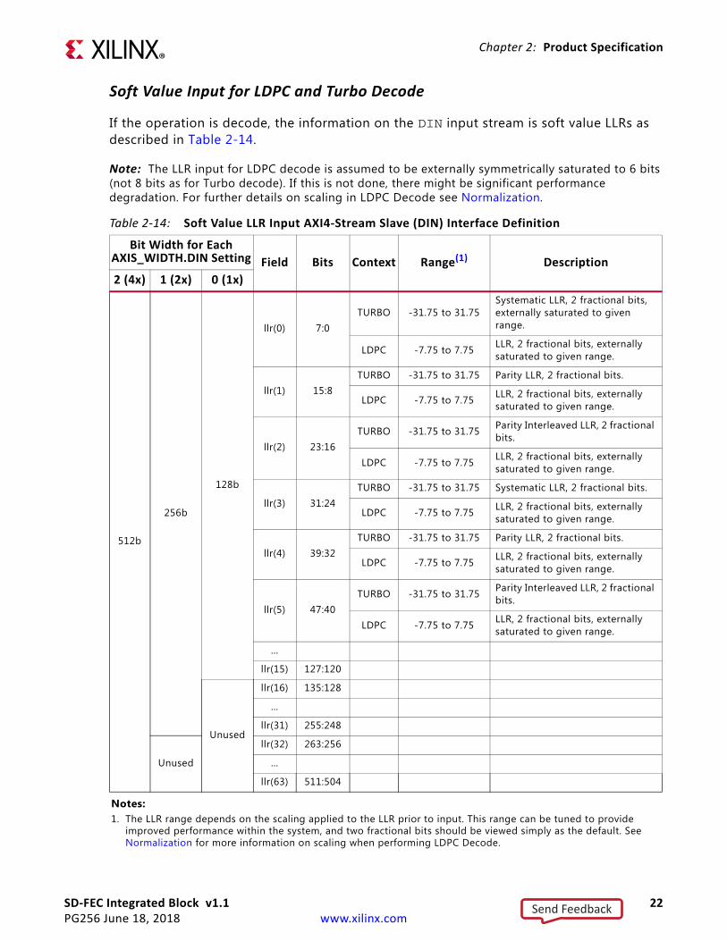
Soft Value Input for LDPC and Turbo Decode
If the operation is decode, the information on the DIN input stream is soft value LLRs as described in Table 2-14.
Note: The LLR input for LDPC decode is assumed to be externally symmetrically saturated to 6 bits (not 8 bits as for Turbo decode). If this is not done, there might be significant performance degradation. For further details on scaling in LDPC Decode see Normalization.
Table 2-14: Soft Value LLR Input AXI4-Stream Slave (DIN) Interface Definition
Bit Width for Each AXIS_WIDTH.DIN Setting Field Bits Context Range(1) Description2 (4x) 1 (2x) 0 (1x)
512b
256b
128b
llr(0) 7:0TURBO -31.75 to 31.75
Systematic LLR, 2 fractional bits, externally saturated to given range.
LDPC -7.75 to 7.75 LLR, 2 fractional bits, externally saturated to given range.
llr(1) 15:8TURBO -31.75 to 31.75 Parity LLR, 2 fractional bits.
LDPC -7.75 to 7.75 LLR, 2 fractional bits, externally saturated to given range.
llr(2) 23:16TURBO -31.75 to 31.75 Parity Interleaved LLR, 2 fractional
bits.
LDPC -7.75 to 7.75 LLR, 2 fractional bits, externally saturated to given range.
llr(3) 31:24TURBO -31.75 to 31.75 Systematic LLR, 2 fractional bits.
LDPC -7.75 to 7.75 LLR, 2 fractional bits, externally saturated to given range.
llr(4) 39:32TURBO -31.75 to 31.75 Parity LLR, 2 fractional bits.
LDPC -7.75 to 7.75 LLR, 2 fractional bits, externally saturated to given range.
llr(5) 47:40TURBO -31.75 to 31.75 Parity Interleaved LLR, 2 fractional
bits.
LDPC -7.75 to 7.75 LLR, 2 fractional bits, externally saturated to given range.
...
llr(15) 127:120
Unused
llr(16) 135:128
…
llr(31) 255:248
Unused
llr(32) 263:256
…
llr(63) 511:504
Notes: 1. The LLR range depends on the scaling applied to the LLR prior to input. This range can be tuned to provide
improved performance within the system, and two fractional bits should be viewed simply as the default. See Normalization for more information on scaling when performing LDPC Decode.
Send Feedback

SD-FEC Integrated Block v1.1 23PG256 June 18, 2018 www.xilinx.com
Chapter 2: Product Specification
Table 2-15 provides an example for the case of LDPC Decoder of how a 5-bit integer range of input is mapped to the soft value (that is, no fractional bits). Note that inputs that are out of range have been saturated (symmetrically).
Note that values in Table 2-15 assume a direct mapping without scaling. Better performance might be achieved by scaling the input by a value less than 1 to reduce or completely avoid saturation. System simulations should be performed to determine the best use of input range for a particular code, channel and symbol mapping. Also, adjustment of the normalization factor might improve performance (where 0.75 is a good starting point).
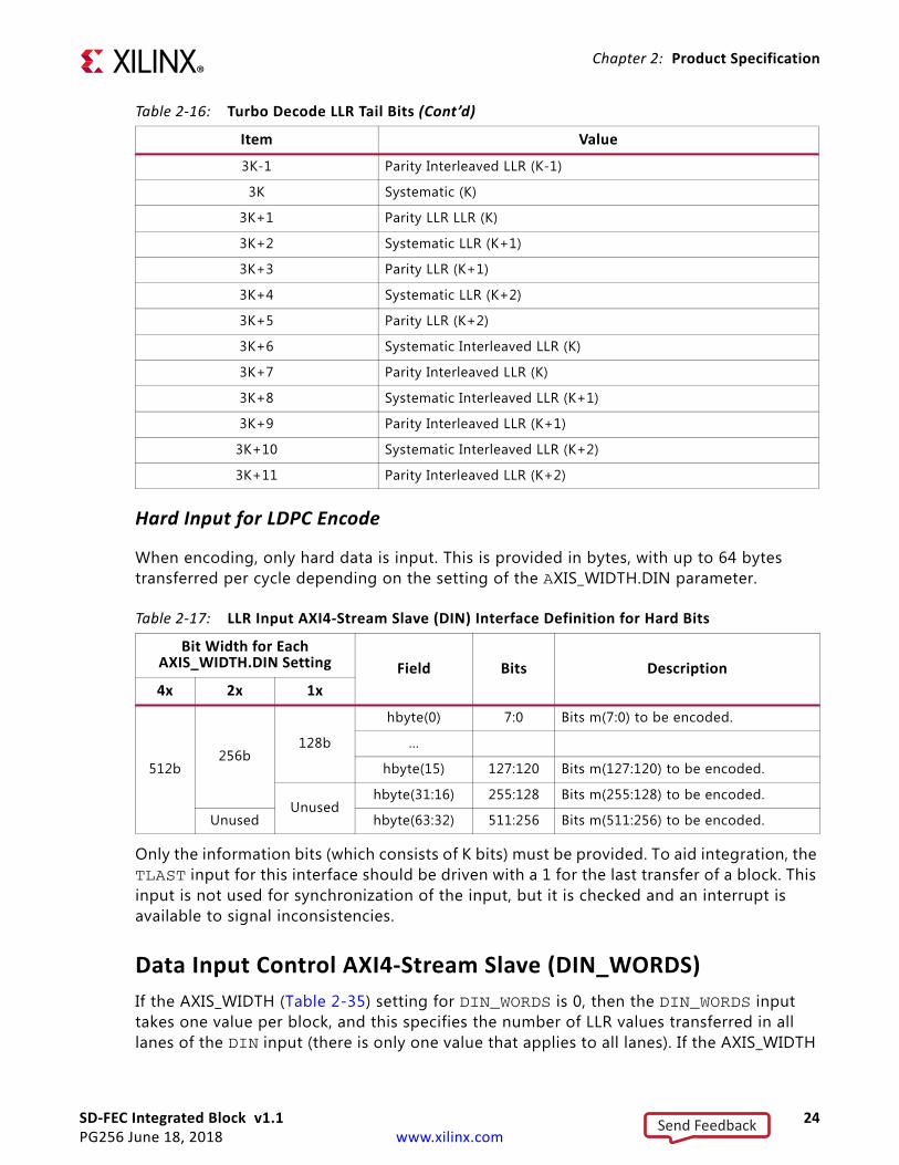
When LLR input is for Turbo Decode, then LLRs for Systematic, Parity and Parity Interleaved are provided interleaved for the K inputs, followed by 12 tail bits as shown in Table 2-16.
Table 2-15: Example Soft Value Mapping for LDPC Decode Input
OriginalValue
Original 5-bit2s Complement
Integer Representation DIN Value DIN input Comment
+15.0 01111 +7.75 00011111 Sign extended and saturated
….
+8.0 01000 +7.75 00011111 Sign extended and saturated
+7.0 00111 +7.0 00011100 Sign extended
+6.0 00110 +6.0 00011000 Sign extended
…
0.0 00000 0.0 00000000 Sign extended
…
-6.0 11010 -6.0 11101000 Sign extended
…
-7.0 11001 -7.0 11100100 Sign extended
-8.0 11000 -7.75 11100001 Sign extended and saturated(symmetrically)
…
-15.0 10001 -7.75 11100001 Sign extended and saturated(symmetrically)
Table 2-16: Turbo Decode LLR Tail Bits
Item Value
0 Systematic LLR (0)
1 Parity LLR (0)
2 Parity Interleaved LLR (0)
… …
3K-3 Systematic LLR (K-1)
3K-2 Parity LLR (K-1)
Send Feedback
SD-FEC Integrated Block v1.1 24PG256 June 18, 2018 www.xilinx.com
Chapter 2: Product Specification
Hard Input for LDPC Encode
When encoding, only hard data is input. This is provided in bytes, with up to 64 bytes transferred per cycle depending on the setting of the AXIS_WIDTH.DIN parameter.
Only the information bits (which consists of K bits) must be provided. To aid integration, the TLAST input for this interface should be driven with a 1 for the last transfer of a block. This input is not used for synchronization of the input, but it is checked and an interrupt is available to signal inconsistencies.
Data Input Control AXI4-Stream Slave (DIN_WORDS)If the AXIS_WIDTH (Table 2-35) setting for DIN_WORDS is 0, then the DIN_WORDS input takes one value per block, and this specifies the number of LLR values transferred in all lanes of the DIN input (there is only one value that applies to all lanes). If the AXIS_WIDTH
3K-1 Parity Interleaved LLR (K-1)
3K Systematic (K)
3K+1 Parity LLR LLR (K)
3K+2 Systematic LLR (K+1)
3K+3 Parity LLR (K+1)
3K+4 Systematic LLR (K+2)
3K+5 Parity LLR (K+2)
3K+6 Systematic Interleaved LLR (K)
3K+7 Parity Interleaved LLR (K)
3K+8 Systematic Interleaved LLR (K+1)
3K+9 Parity Interleaved LLR (K+1)
3K+10 Systematic Interleaved LLR (K+2)
3K+11 Parity Interleaved LLR (K+2)
Table 2-17: LLR Input AXI4-Stream Slave (DIN) Interface Definition for Hard Bits
Bit Width for Each AXIS_WIDTH.DIN Setting Field Bits Description4x 2x 1x
512b256b
128b
hbyte(0) 7:0 Bits m(7:0) to be encoded.
…
hbyte(15) 127:120 Bits m(127:120) to be encoded.
Unusedhbyte(31:16) 255:128 Bits m(255:128) to be encoded.
Unused hbyte(63:32) 511:256 Bits m(511:256) to be encoded.
Table 2-16: Turbo Decode LLR Tail Bits (Cont’d)
Item Value
Send Feedback

SD-FEC Integrated Block v1.1 25PG256 June 18, 2018 www.xilinx.com
Chapter 2: Product Specification
setting for each transfer is 1, then the number of bytes transferred per cycle on DIN is specified by DIN_WORDS. To aid integration, the TLAST input for this interface should be driven with a 1 for the last transfer of a block. This input is not used to synchronize the input, but it is checked and an interrupt is available to signal inconsistencies.
Note: If DIN_WORDS is 0, then there is only one transfer per block and so it is expected that TLAST is driven High on each transfer on this stream.
If the data input interface is configured for soft input (that is, a decode operation is being performed), then the LLR input words (DIN_WORDS) stream specifies the number of LLR values in the respective lane of input.
If DIN is configured for hard input (that is, an LDPC encode operation is being performed), then DIN_WORDS specifies the number of bytes of hard bits transferred per cycle. In both cases, data bytes in DIN lanes are always in the least significant bytes of the DIN lane, for example, if two bytes of soft or hard bits are provided in lane 0, they are in bits 7:0 and 15:8.
DIN_WORDS is internally overridden to ensure that multiple blocks do not straddle a transaction on DIN, and the final transaction is shortened, if necessary, by reducing the bytes transferred. For example, if AXIS_WIDTH.DIN_WORDS setting is 0, such that a single value is used over the whole block, if the block is not a multiple of the DIN_WORDS value, then the last transfer is reduced to match the actual block size. Similarly, if four lanes are in use, and DIN_WORDS is 8, 4, 2, 1 on the respective lanes 0 to 3, and there are 13 words remaining, then 8 and 4 words are transferred on lanes 0 and 1, and one word on lane 2 and zero words on lane 3. As such it is possible to keep DIN_WORDS constant over a block even if the block length is not a multiple of DIN_WORDS.
Table 2-18: LLR Input AXI4-Stream Slave (DIN_WORDS) Interface Definition
AXIS_WIDTH.DIN_WORDS
Setting
Bit Width for EachAXIS_WIDTH.DIN Setting Field Bits Range Description
4x 2x 1x
0 8b
8b8b
words 7:0 0-16
Number of input data words in din(127…0)
Unused
Number of input data words in din(255…128)
Unused
Number of input data words in din(383…256)
Number of input data words in din(511…384)
1 32b
16b8b words(0) 7:0 0-16 Number of input data words in
din(127…0)
Unused
words (1) 15:8 0-16 Number of input data words in din(255…128)
Unusedwords (2) 23:16 0-16 Number of input data words in
din(383…256)
words (3) 31:24 0-16 Number of input data words in din(511…384)
Send Feedback
SD-FEC Integrated Block v1.1 26PG256 June 18, 2018 www.xilinx.com
Chapter 2: Product Specification
Data Output AXI4-Stream Master (DOUT)• The DOUT data output stream consists of four 128-bit lanes. The number of lanes
depends on the setting of the AXIS_WIDTH.DOUT parameter.
• When decoding, either bytes of LLR or bytes of hard bits are transferred over DOUT, depending on the hard_op setting in the input to CTRL for the associated block. When encoding, only hard data is transferred over DOUT, and there it no hard_op setting in the input CTRL.
• Blocks are transferred over one or more cycles, starting with the least significant LLR or hard bits first.
• The number of bytes transferred over DOUT on each cycle is given by the DOUT_WORDS input stream. See LLR Output Words (DOUT_WORDS) for details on how DOUT_WORDS is used.
• Data bytes are transferred in the least significant bytes of each DOUT lane. For example, if DOUT_WORDS specifies two bytes are transferred in lane 0, then these bytes are in llr(0) and llr(1) (in bits 7:0 and 15:8).
• Each transfer can only contain one block; one block must complete before the next block can start. For multi-lane transfers, this might require the final transfer to have one or more of the higher lanes size set to zero or one of the lane values to be reduced. The core enforces this internally on output so that blocks start on lane 0 of the next AXI4-Stream transaction.
Send Feedback

SD-FEC Integrated Block v1.1 27PG256 June 18, 2018 www.xilinx.com
Chapter 2: Product Specification
Soft Output for LDPC and Turbo Decode
Hard Output for LDPC and Turbo Decode and LDPC Encode
When hard_op=1 then only hard bits are output. This is provided in bytes, with up to 64 bytes transferred per cycle dependent on the setting of AXIS_WIDTH.DOUT parameter as summarized by Table 2-20.
Table 2-19: LLR Output AXI4-Stream Master (DOUT) TDATA Interface Definition
Bit Width for EachAXIS_WIDTH.DOUT Setting Field Bits Context Range Description2 (4x) 1 (2x) 0 (1x)
512b
256b
128b
llr(0) 7:0TURBO -31.75 to 31.75 Systematic LLR, 2 fractional
bits
LDPC -31.75 to 31.75 LLR, 2 fractional bits
llr(1) 15:8TURBO -31.75 to 31.75 Parity LLR, 2 fractional bits
LDPC -31.75 to 31.75 LLR, 2 fractional bits
llr(2) 23:16TURBO -31.75 to 31.75 Parity Interleaved LLR, 2
fractional bits
LDPC -31.75 to 31.75 LLR, 2 fractional bits
...
llr(15) 127:120
Unused
llr(16) 135:128
…
llr(31) 255:248
Unused
llr(32) 263:256
…
llr(63) 511:504
Table 2-20: LLR Output AXI4-Stream Slave (DOUT) Interface Definition Configured for Hard Bits
Bit Width for EachAXIS_WIDTH.DOUT Setting Field Bits Description
4x 2x 1x
512b256b
128b
hbyte(0) 7:0 Bits m(7:0)
…
hbyte(15) 127:120 Bits m(127:120)
Unused hbyte(31:16) 255:128 Bits m(255:128)
Unused hbyte(63:32) 511:256 Bits m(511:256)
Send Feedback

SD-FEC Integrated Block v1.1 28PG256 June 18, 2018 www.xilinx.com
Chapter 2: Product Specification
LLR Output Words (DOUT_WORDS)If the AXIS_WIDTH parameter setting for the DOUT_WORDS field is 0, then the DOUT_WORDS input takes one value per block, and this specifies the number of LLR values transferred on all lanes of DOUT.
If the AXIS_WIDTH parameter setting for DOUT_WORDS field is 1, then the number of bytes transferred per cycle on DOUT is specified on a transfer-by-transfer basis by DOUT_WORDS. To aid integration the TLAST input for this interface should be driven with a 1 for the last transfer of a block. This input is not used to synchronize output, but it is checked and an interrupt is available to signal inconsistencies.
Note: If DOUT_WORDS is 0, then there is only one transfer per block and so it is expected that TLAST is driven High on each transfer on this stream.
If the data interface is configured for soft output (that is, a decode operation is being performed and hard_op is 0), then the DOUT_WORDS stream specifies the number of LLR values in the respective lane of output.
If DOUT is configured for hard output, then DOUT_WORDS specifies the number of bytes of hard output transferred per cycle (only multiples of 8 bits can be specified). In both cases, data words in DOUT lanes are always in the least significant bytes of the DOUT lane, for example, if two words are provided in lane 0, they are in bits 7:0 and 15:8.
DOUT_WORDS is internally overridden to ensure that multiple blocks do not straddle a transaction on DOUT (the final transaction is shortened, if necessary, in the same way as for DIN_WORDS as described in Data Input Control AXI4-Stream Slave (DIN_WORDS)). As such it is possible to keep DOUT_WORDS constant over a block even if the block length is not a multiple of DOUT_WORDS.
If operating out-of-order, with AXIS_WIDTH.DOUT_WORDS=1, and mixed block lengths, then the STATUS output can be used to determine the number of outputs, to set TLAST (if used). The STATUS output can also be used to set DOUT_WORDS if it is being changed on a block-by-block basis. If TLAST is not being used, then TLAST interrupts can be masked on this interface to avoid unnecessary interrupts (see Interrupt Mask Register Table 2-42).
Send Feedback

SD-FEC Integrated Block v1.1 29PG256 June 18, 2018 www.xilinx.com
Chapter 2: Product Specification
Throughput Limits of InterfacesWhile the data interfaces support wide transfer widths, internally the throughput of the input and output interfaces is limited to a maximum of:
• Turbo decode: 12 LLRs @f(core_clk)
• LDPC decode: 16 LLRs or 16 hard bytes @f(core_clk)
• LDPC encode: 16 hard bytes @f(core_clk)
Turbo Decoder Interface Throughput Limit
For Turbo decode, the internal interface throughput limit is 12 LLRs per core_clk cycle, consisting of four sets of three 8-bit values (systematic, parity, parity interleaved). If parity is not required at the output, then the limit is four systematic LLR values per core_clk cycle. If hard output is required, then the limit is still four systematic values per core_clk cycle, but the four values are now hard bits.
Table 2-21: LLR Output Words AXI4-Stream Slave (DOUT_WORDS) Interface Definition
AXIS_WIDTH.DOUT_WORDS
Setting
Bit Width for Each AXIS_WIDTH.DOUT
Setting Field Bits Range Description
4x 2x 1x
0 8b
8b8b
words 7:0 0-16
Number of output data words in dout(127…0)
Unused
Number of output data words in dout(255…128)
Unused
Number of output data words in dout(383…256)
Number of output data words in dout(511…384)
1 32b
16b8b words(0) 7:0 0-16 Number of output data words
in dout(127…0)
Unused
words (1) 15:8 0-16 Number of output data words in dout(255…128)
Unusedwords (2) 23:16 0-16 Number of output data words
in dout(383…256)
words (3) 31:24 0-16 Number of output data words in dout(511…384)
Send Feedback

SD-FEC Integrated Block v1.1 30PG256 June 18, 2018 www.xilinx.com
Chapter 2: Product Specification
LDPC Decoder Interface Throughput Limit
For the decoder, if the LDPC sub-matrix size, P, is not a multiple of 16, then not all internal transfers into internal input memory are 16 LLRs. Transfers are in groups of P, and the final transfer in a group is mod(P, 16), and the average I/O throughput is reduced to:
LLRs per second Equation 2-2
For example, if P=27, then the peak I/O B/W is:
(for example, ~9G LLRs per second at fcore_clk= 667 MHz)
LDPC Encoder Interface Throughput Limit
For the encoder, transfers are at most 16 bytes, or 128 bits. If P<128 then at most P bits are transferred between interface and memory per cycle and the average I/O throughput becomes:
Gb/s Equation 2-3
For example, if P=360, then peak hard bits I/O B/W is:
(for example, 80 Gb/s at fcore_clock = 667 MHz)
These limits provide lower limits on increased throughput possible with small numbers of iterations.
AXI4-Stream InterfaceThe AXI4-Stream interface is a point to point link where the transmitter is known as a master, and the receiver a slave. For further details on AXI4-Stream interfaces see the AMBA® AXI4-Stream Protocol Specification (ARM IHI 0051A) [Ref 9] and the Vivado Design Suite AXI Reference Guide (UG1037) [Ref 10].
Basic Handshake
Figure 2-3 shows the transfer of data in an AXI4-Stream channel. tvalid is driven by the source (master) side of the channel and tready is driven by the destination (slave) side. tvalid indicates that the values in the payload fields (tdata and tlast) are valid. tready
LLR I/O B/W PP16-----
----------- fcore_clk×=
LDPC LLR I/O B/W 272716-----
----------- fcore_clk×=
LDPC hard bits I/O B/W PP
128--------
------------- fcore_clk×=
LDPC hard bits I/O B/W 360360128--------
------------- fcore_clk×=
Send Feedback

SD-FEC Integrated Block v1.1 31PG256 June 18, 2018 www.xilinx.com
Chapter 2: Product Specification
indicates that the slave is ready to accept data. When both tvalid and tready are asserted in the same clock cycle, a transfer occurs.
Note: The order of tvalid or tready going High or Low is not important; data is only transferred when both tvalid and tready are High.
Use of TLAST
The core always produces tlast signals on all output channels; however the sizes of input packets are always either fixed or given explicitly using associated control information. Hence the tlast on input channels is actually redundant; requiring a source to provide a suitable tlast could hinder interoperability. Therefore the core has been specifically designed to ignore tlast inputs for packet delineation and use internal knowledge of packet size instead. In all such cases, the core also produces two event signals, one to indicate tlast was unexpectedly asserted (tlast unexpected events) and one to indicate tlast was unexpectedly deasserted (tlast missing events). In all situations the core continues to operate as if tlast was correctly applied, and the events can be interpreted as required. For further details of tlast handling in Xilinx® IP see the Vivado Design Suite AXI Reference Guide (UG1037) [Ref 10].
Note: When a packet consists of a single transfer of data, tlast is redundant and should be tied off to 1.
AXI4-Lite InterfaceFor details on AXI4-Lite interfaces see the AMBA AXI and ACE Protocol Specification (ARM IHI0022E) [Ref 1], and the Vivado Design Suite AXI Reference Guide (UG1037) [Ref 10].
X-Ref Target - Figure 2-3
Figure 2-3: Data Transfer in an AXI4-Stream Channel
Send Feedback

SD-FEC Integrated Block v1.1 32PG256 June 18, 2018 www.xilinx.com
Chapter 2: Product Specification
Standards• Turbo decode required by the LTE standard is defined in:
° 3GPP TS 36.212 Multiplexing and channel coding [Ref 14]
• LDPC codes required for the following standards are provided by the core:
° WiFi 802.11ac-2012 High Throughput PHY [Ref 13]
° DOCSIS 3.1 OFDM PHY [Ref 12]
° 3GPP TS 38.212 V.15.0.0 Multiplexing and channel coding (Release 15) [Ref 11]
• 3GPP TS 38.212 V.15.0.0 (2017-12) NR; Multiplexing and channel coding (Release 15) [Ref 11]
PerformanceIn the following sections clock frequencies of 667 MHz on core_clk and 400 MHz on other clocks are assumed, and the decoder uses eight iterations. However, for details on the clock frequency supported by a device and resource utilization, visit the Performance and Resource Utilization web page. Packing is assumed to be enabled; if disabled, then for codes with PSIZE ≤ 64 there is likely to be a significant throughput reduction.
LDPC Decoding and EncodingThroughput and Latency
Throughput is measured in terms of information bits per second, including any punctured bits. In the following sections, the throughput has been measured by inputting the data as quickly as possible. The tables provide the time of the start and end of the first input block and the start and end of the output data of the first, 84th 96th and 100th blocks, relative to the start of the first block that was input. Initial Latency is the time between the last transfer of the first input block and the last output of the first output block. The assumption here is that the LDPC code parameters and shared LDPC code parameters in the SD-FEC hard block are already configured for the particular code. Final throughput is the throughput from blocks 84 to 96. Note that the number 12 has been used, as this is a multiple of 1, 2, 3 and 4, which is the number of blocks that can be decoded simultaneously. The assumptions are that the output is not held up and that the decoder measurement is performed with hard output that does not include parity.
Note that the latency of later blocks is likely to be greater than the initial latency due to input buffering holding additional blocks, and can often be reduced by feeding in the blocks at a steady rate, commensurate with the throughput, to avoid them building up in the input buffer. It is also possible, for some codes, to have a reduced latency with a small reduction
Send Feedback

Chapter 2: Product Specification
SD-FEC Integrated Block v1.1 33PG256 June 18, 2018 www.xilinx.com
in throughput, because of the way the core schedules multiple blocks, and lower throughput can mean fewer blocks interleaved and lower latency as a result.
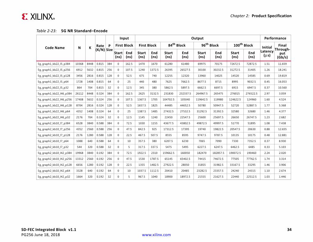
5G New Radio
Throughput and latency figures for the 5G New Radio (NR) standard are shown in Table 2-22 and Table 2-23.Table 2-22: 5G NR Standard–Decode
Code Name N K Rate(K/N)
PSize
Input Output Performance
InitialLatency
(μs)
FinalThrough-
put(Gb/s)
First Block First Block 84th Block 96th Block 100th Block
Start(ns)
End(ns)
Start(ns)
End(ns)
Start(ns)
End(ns)
Start(ns)
End(ns)
Start(ns)
End(ns)
5g_graph1_kb22_l5_p384 10368 8448 0.815 384 0 1617.5 8255 8417.5 331397.5 331560 378252.5 378415 392717.5 392880 6.80 2.164
5g_graph1_kb22_l5_p256 6912 5632 0.815 256 0 1077.5 5892.5 6000 180987.5 181095 206150 206257.5 211475 211582.5 4.92 2.686
5g_graph1_kb22_l5_p128 3456 2816 0.815 128 0 537.5 3135 3187.5 85555 85607.5 97442.5 97495 100167.5 100220 2.65 2.843
5g_graph1_kb22_l5_p64 1728 1408 0.815 64 0 267.5 2007.5 2037.5 45565 45595 51902.5 51932.5 53567.5 53597.5 1.77 2.666
5g_graph1_kb22_l5_p32 864 704 0.815 32 0 132.5 1500 1525 30317.5 30345 34562.5 34590 35860 35887.5 1.39 1.990
5g_graph1_kb22_l46_p384 26112 8448 0.324 384 0 4077.5 23777.5 23940 1665807.5 1665970 1903210 1903372.5 1982345 1982507.5 19.86 0.427
5g_graph1_kb22_l46_p256 17408 5632 0.324 256 0 2717.5 14142.5 14250 960965 961072.5 1097855 1097962.5 1143485 1143592.5 11.53 0.494
5g_graph1_kb22_l46_p128 8704 2816 0.324 128 0 1357.5 12997.5 13050 340260 340312.5 388222.5 388275 405645 405697.5 11.69 0.705
5g_graph1_kb22_l46_p64 4352 1408 0.324 64 0 677.5 11015 11045 227337.5 227367.5 259412.5 259442.5 269407.5 269437.5 10.37 0.527
5g_graph1_kb22_l46_p32 2176 704 0.324 32 0 337.5 9600 9627.5 194720 194747.5 222332.5 222360 231205 231232.5 9.29 0.306
5g_graph2_kb10_l7_p384 6528 3840 0.588 384 0 1017.5 6440 6512.5 245782.5 245855 280595 280667.5 291747.5 291820 5.50 1.324
5g_graph2_kb10_l7_p256 4352 2560 0.588 256 0 677.5 4477.5 4525 109952.5 110000 125307.5 125355 129547.5 129595 3.85 2.001
5g_graph2_kb10_l7_p128 2176 1280 0.588 128 0 337.5 2562.5 2585 54382.5 54405 61947.5 61970 64142.5 64165 2.25 2.030
5g_graph2_kb10_l7_p64 1088 640 0.588 64 0 167.5 1750 1762.5 34217.5 34230 39002.5 39012.5 40542.5 40555 1.59 1.606
5g_graph2_kb10_l7_p32 544 320 0.588 32 0 82.5 1520 1527.5 29262.5 29270 33382.5 33392.5 34752.5 34762.5 1.44 0.931
5g_graph2_kb10_l42_p384 19968 3840 0.192 384 0 3117.5 18747.5 18820 1316535 1316607.5 1504167.5 1504240 1566712.5 1566785 15.70 0.246
5g_graph2_kb10_l42_p256 13312 2560 0.192 256 0 2077.5 14037.5 14085 490017.5 490065 559030 559077.5 581315 581362.5 12.01 0.445
5g_graph2_kb10_l42_p128 6656 1280 0.192 128 0 1037.5 10272.5 10295 211375 211397.5 240950 240972.5 249905 249927.5 9.26 0.519
5g_graph2_kb10_l42_p64 3328 640 0.192 64 0 517.5 8682.5 8695 175220 175232.5 199937.5 199950 207787.5 207800 8.18 0.311
5g_graph2_kb10_l42_p32 1664 320 0.192 32 0 257.5 8245 8255 167365 167375 191117.5 191125 198770 198777.5 8.00 0.162
Chapter 2: Product Specification
SD-FEC Integrated Block v1.1 34PG256 June 18, 2018 www.xilinx.com
Table 2-23: 5G NR Standard–Encode
Code Name N K Rate(K/N)
PSize
Input Output Performance
InitialLatency
(μs)
FinalThrough-
put(Gb/s)
First Block First Block 84th Block 96th Block 100th Block
Start(ns)
End(ns)
Start(ns)
End(ns)
Start(ns)
End(ns)
Start(ns)
End(ns)
Start(ns)
End(ns)
5g_graph1_kb22_l5_p384 10368 8448 0.815 384 0 162.5 1470 1670 61280 61480 69975 70175 72672.5 72872.5 1.51 11.659
5g_graph1_kb22_l5_p256 6912 5632 0.815 256 0 107.5 1240 1372.5 26395 26527.5 30100 30232.5 31272.5 31405 1.26 18.241
5g_graph1_kb22_l5_p128 3456 2816 0.815 128 0 52.5 675 740 12255 12320 13960 14025 14520 14585 0.69 19.819
5g_graph1_kb22_l5_p64 1728 1408 0.815 64 0 25 440 480 7625 7662.5 8677.5 8715 8995 9032.5 0.45 16.053
5g_graph1_kb22_l5_p32 864 704 0.815 32 0 12.5 345 380 5862.5 5897.5 6662.5 6697.5 6915 6947.5 0.37 10.560
5g_graph1_kb22_l46_p384 26112 8448 0.324 384 0 162.5 2625 3132.5 231830 232337.5 264967.5 265475 276015 276522.5 2.97 3.059
5g_graph1_kb22_l46_p256 17408 5632 0.324 256 0 107.5 1367.5 1705 104702.5 105040 119642.5 119980 124622.5 124960 1.60 4.524
5g_graph1_kb22_l46_p128 8704 2816 0.324 128 0 52.5 1657.5 1825 44485 44652.5 50780 50947.5 52720 52887.5 1.77 5.368
5g_graph1_kb22_l46_p64 4352 1408 0.324 64 0 25 1387.5 1485 27432.5 27532.5 31292.5 31392.5 32580 32680 1.46 4.377
5g_graph1_kb22_l46_p32 2176 704 0.324 32 0 12.5 1145 1240 22450 22547.5 25600 25697.5 26650 26747.5 1.23 2.682
5g_graph2_kb10_l7_p384 6528 3840 0.588 384 0 72.5 1030 1155 43677.5 43802.5 49872.5 49997.5 51770 51895 1.08 7.438
5g_graph2_kb10_l7_p256 4352 2560 0.588 256 0 47.5 842.5 925 17312.5 17395 19740 19822.5 20547.5 20630 0.88 12.655
5g_graph2_kb10_l7_p128 2176 1280 0.588 128 0 22.5 467.5 507.5 8555 8595 9747.5 9787.5 10135 10175 0.48 12.881
5g_graph2_kb10_l7_p64 1088 640 0.588 64 0 10 357.5 380 6207.5 6230 7065 7090 7330 7352.5 0.37 8.930
5g_graph2_kb10_l7_p32 544 320 0.588 32 0 5 317.5 337.5 5475 5495 6227.5 6247.5 6462.5 6485 0.33 5.103
5g_graph2_kb10_l42_p384 19968 3840 0.192 384 0 72.5 1922.5 2310 159662.5 160050 182470 182857.5 190072.5 190460 2.24 2.020
5g_graph2_kb10_l42_p256 13312 2560 0.192 256 0 47.5 1530 1787.5 65145 65402.5 74415 74672.5 77505 77762.5 1.74 3.314
5g_graph2_kb10_l42_p128 6656 1280 0.192 128 0 22.5 1355 1482.5 27922.5 28050 31855 31982.5 33167.5 33295 1.46 3.906
5g_graph2_kb10_l42_p64 3328 640 0.192 64 0 10 1037.5 1112.5 20410 20485 23282.5 23357.5 24240 24315 1.10 2.674
5g_graph2_kb10_l42_p32 1664 320 0.192 32 0 5 967.5 1040 18900 18972.5 21555 21627.5 22440 22512.5 1.03 1.446

SD-FEC Integrated Block v1.1 35PG256 June 18, 2018 www.xilinx.com
Chapter 2: Product Specification
In 5G NR mode, the 5G support logic generates and downloads LDPC Code and Shared LDPC Code Parameters for the code definition applied through the CTRL interface. The download latency in each case is provided in Table 2-24. For throughput enhancement, write the code definitions through the CTRL interface as early as possible compared to the input data to minimize the impact of code latency and enhance throughput. However, care must be taken not to apply more CTRL words than the corresponding code blocks in a given transmission time interval.
The 5G support logic also keeps log of, at most, 14 codes downloaded to the SD-FEC core at any given time to avoid the need to regenerate and re-download the same code.
Table 2-24: Download Latency
No.Code Type Latency of Code Download
(Cycles)bg kb mb Z (PSIZE)
1 0 22 46 2 ≤ Z ≤ 32 852
2 0 22 46 32 < Z ≤ 64 651
3 0 22 46 64 < Z ≤ 384 554
4 1 10 42 2 ≤ Z ≤ 32 631
5 1 10 42 32 < Z ≤ 64 472
6 1 10 42 64 < Z ≤ 384 394
7 2 9 42 2 ≤ Z ≤ 32 606
8 2 9 42 32 < Z ≤ 64 442
9 2 9 42 64 < Z ≤ 128 384
10 3 8 42 2 ≤ Z ≤ 32 614
11 3 8 42 32 < Z ≤ 64 456
12 3 8 42 64 < Z ≤ 128 376
13 4 6 42 2 ≤ Z ≤ 32 572
14 4 6 42 32 < Z ≤ 64 432
15 4 6 42 64 < Z ≤ 128 351
Send Feedback
Chapter 2: Product Specification
SD-FEC Integrated Block v1.1 36PG256 June 18, 2018 www.xilinx.com
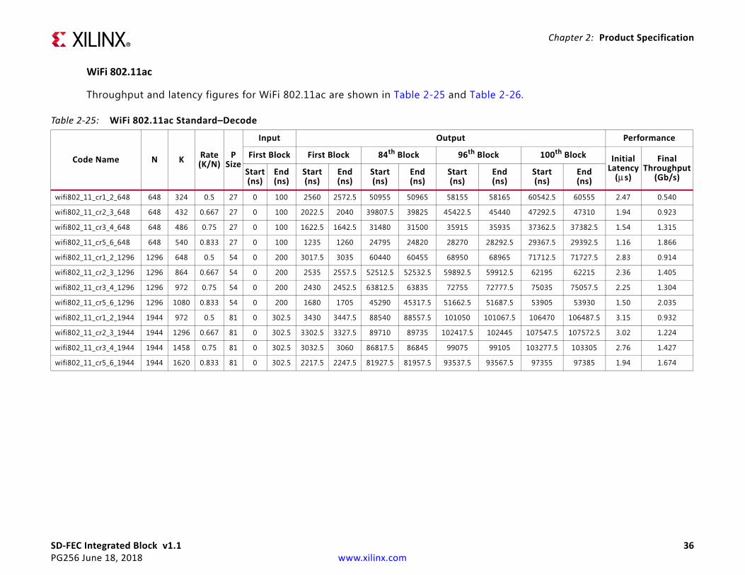
WiFi 802.11ac
Throughput and latency figures for WiFi 802.11ac are shown in Table 2-25 and Table 2-26.
Table 2-25: WiFi 802.11ac Standard–Decode
Code Name N K Rate(K/N)
PSize
Input Output Performance
InitialLatency
(μs)
FinalThroughput
(Gb/s)
First Block First Block 84th Block 96th Block 100th Block
Start(ns)
End(ns)
Start(ns)
End(ns)
Start(ns)
End(ns)
Start(ns)
End(ns)
Start(ns)
End(ns)
wifi802_11_cr1_2_648 648 324 0.5 27 0 100 2560 2572.5 50955 50965 58155 58165 60542.5 60555 2.47 0.540
wifi802_11_cr2_3_648 648 432 0.667 27 0 100 2022.5 2040 39807.5 39825 45422.5 45440 47292.5 47310 1.94 0.923
wifi802_11_cr3_4_648 648 486 0.75 27 0 100 1622.5 1642.5 31480 31500 35915 35935 37362.5 37382.5 1.54 1.315
wifi802_11_cr5_6_648 648 540 0.833 27 0 100 1235 1260 24795 24820 28270 28292.5 29367.5 29392.5 1.16 1.866
wifi802_11_cr1_2_1296 1296 648 0.5 54 0 200 3017.5 3035 60440 60455 68950 68965 71712.5 71727.5 2.83 0.914
wifi802_11_cr2_3_1296 1296 864 0.667 54 0 200 2535 2557.5 52512.5 52532.5 59892.5 59912.5 62195 62215 2.36 1.405
wifi802_11_cr3_4_1296 1296 972 0.75 54 0 200 2430 2452.5 63812.5 63835 72755 72777.5 75035 75057.5 2.25 1.304
wifi802_11_cr5_6_1296 1296 1080 0.833 54 0 200 1680 1705 45290 45317.5 51662.5 51687.5 53905 53930 1.50 2.035
wifi802_11_cr1_2_1944 1944 972 0.5 81 0 302.5 3430 3447.5 88540 88557.5 101050 101067.5 106470 106487.5 3.15 0.932
wifi802_11_cr2_3_1944 1944 1296 0.667 81 0 302.5 3302.5 3327.5 89710 89735 102417.5 102445 107547.5 107572.5 3.02 1.224
wifi802_11_cr3_4_1944 1944 1458 0.75 81 0 302.5 3032.5 3060 86817.5 86845 99075 99105 103277.5 103305 2.76 1.427
wifi802_11_cr5_6_1944 1944 1620 0.833 81 0 302.5 2217.5 2247.5 81927.5 81957.5 93537.5 93567.5 97355 97385 1.94 1.674

Chapter 2: Product Specification
SD-FEC Integrated Block v1.1 37PG256 June 18, 2018 www.xilinx.com
Table 2-26: WiFi 802.11ac Standard–Encode
Code Name N K Rate(K/N)
PSize
Input Output Performance
InitialLatency
(μs)
FinalThroughput
(Gb/s)
First Block First Block 84th Block 96th Block 100th Block
Start(ns)
End(ns)
Start(ns)
End(ns)
Start(ns)
End(ns)
Start(ns)
End(ns)
Start(ns)
End(ns)
wifi802_11_cr1_2_648 648 324 0.5 27 0 5 540 570 11380 11410 12982.5 13012.5 13515 13545 0.56 2.426
wifi802_11_cr2_3_648 648 432 0.667 27 0 7.5 370 400 7932.5 7962.5 9040 9070 9407.5 9437.5 0.39 4.681
wifi802_11_cr3_4_648 648 486 0.75 27 0 7.5 362.5 392.5 6937.5 6967.5 7900 7930 8210 8240 0.39 6.059
wifi802_11_cr5_6_648 648 540 0.833 27 0 10 272.5 305 4902.5 4935 5575 5605 5787.5 5817.5 0.29 9.672
wifi802_11_cr1_2_1296 1296 648 0.5 54 0 12.5 655 690 13145 13180 15000 15032.5 15612.5 15645 0.68 4.198
wifi802_11_cr2_3_1296 1296 864 0.667 54 0 15 520 555 10107.5 10140 11525 11557.5 11985 12020 0.54 7.314
wifi802_11_cr3_4_1296 1296 972 0.75 54 0 17.5 542.5 577.5 10025 10060 11430 11462.5 11882.5 11917.5 0.56 8.317
wifi802_11_cr5_6_1296 1296 1080 0.833 54 0 20 425 460 7487.5 7522.5 8527.5 8560 8850 8882.5 0.44 12.492
wifi802_11_cr1_2_1944 1944 972 0.5 81 0 17.5 887.5 925 17657.5 17695 20155 20192.5 20987.5 21025 0.91 4.670
wifi802_11_cr2_3_1944 1944 1296 0.667 81 0 25 772.5 810 14977.5 15015 17087.5 17125 17777.5 17815 0.78 7.371
wifi802_11_cr3_4_1944 1944 1458 0.75 81 0 27.5 722.5 760 13760 13797.5 15695 15732.5 16322.5 16360 0.73 9.042
wifi802_11_cr5_6_1944 1944 1620 0.833 81 0 30 655 692.5 12272.5 12310 13990 14027.5 14527.5 14565 0.66 11.319
Chapter 2: Product Specification
SD-FEC Integrated Block v1.1 38PG256 June 18, 2018 www.xilinx.com
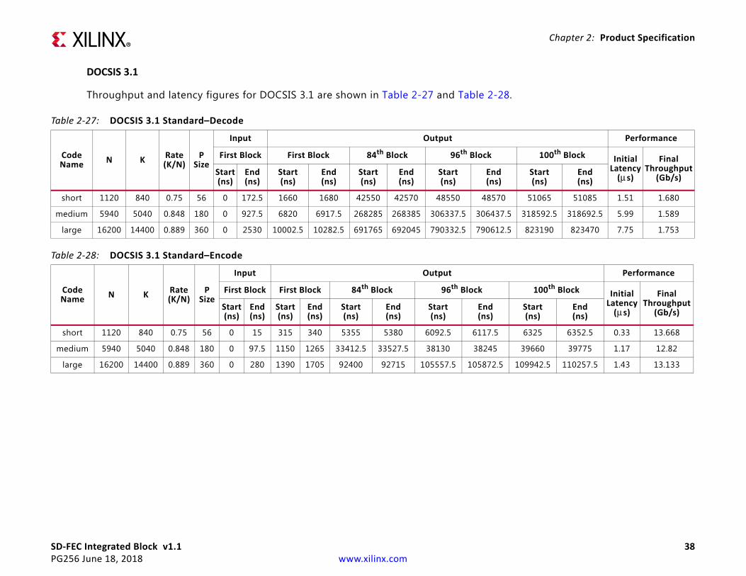
DOCSIS 3.1
Throughput and latency figures for DOCSIS 3.1 are shown in Table 2-27 and Table 2-28.
Table 2-27: DOCSIS 3.1 Standard–Decode
Code Name N K Rate
(K/N)P
Size
Input Output Performance
InitialLatency
(μs)
FinalThroughput
(Gb/s)
First Block First Block 84th Block 96th Block 100th Block
Start(ns)
End(ns)
Start(ns)
End(ns)
Start(ns)
End(ns)
Start(ns)
End(ns)
Start(ns)
End(ns)
short 1120 840 0.75 56 0 172.5 1660 1680 42550 42570 48550 48570 51065 51085 1.51 1.680
medium 5940 5040 0.848 180 0 927.5 6820 6917.5 268285 268385 306337.5 306437.5 318592.5 318692.5 5.99 1.589
large 16200 14400 0.889 360 0 2530 10002.5 10282.5 691765 692045 790332.5 790612.5 823190 823470 7.75 1.753
Table 2-28: DOCSIS 3.1 Standard–Encode
Code Name N K Rate
(K/N)P
Size
Input Output Performance
InitialLatency
(μs)
FinalThroughput
(Gb/s)
First Block First Block 84th Block 96th Block 100th Block
Start(ns)
End(ns)
Start(ns)
End(ns)
Start(ns)
End(ns)
Start(ns)
End(ns)
Start(ns)
End(ns)
short 1120 840 0.75 56 0 15 315 340 5355 5380 6092.5 6117.5 6325 6352.5 0.33 13.668
medium 5940 5040 0.848 180 0 97.5 1150 1265 33412.5 33527.5 38130 38245 39660 39775 1.17 12.82
large 16200 14400 0.889 360 0 280 1390 1705 92400 92715 105557.5 105872.5 109942.5 110257.5 1.43 13.133

SD-FEC Integrated Block v1.1 39PG256 June 18, 2018 www.xilinx.com
Chapter 2: Product Specification
BER Performance
5G New Radio
The 5G New Radio (NR) BER performance is shown in Figure 2-4, Figure 2-5, and Figure 2-6. This includes puncturing of the first 2*Z information bits (where Z=PSIZE). For each SNR point, groups of 4800 frames have been run until 75 frame errors have occurred. The decoder has been configured with a maximum of 32 iterations and early termination on parity pass. BPSK modulation and LLR demodulation has been used along with an AWGN channel. Additional LLR scaling has been applied at the input of the decode to maximize its dynamic range. Table 2-29 shows the scaling factors used. Table 2-30 shows the normalization factors used for each codes.
Table 2-29: Scaling Factors
SNR LLR Scaling SNR LLR Scaling SNR LLR Scaling
-5 1.9375 -0.5 1.03125 4 0.53125
-4.75 1.875 -0.25 1 4.25 0.5
-4.5 1.78125 0 0.96875 4.5 0.5
-4.25 1.78125 0.25 0.9375 4.75 0.46875
-4 1.65625 0.5 0.90625 5 0.46875
-3.75 1.625 0.75 0.875 5.25 0.4375
-3.5 1.5625 1 0.84375 5.5 0.4375
-3.25 1.53125 1.25 0.8125 5.75 0.40625
-3 1.4375 1.5 0.78125 6 0.40625
-2.75 1.40625 1.75 0.75 6.25 0.375
-2.5 1.375 2 0.71875 6.5 0.375
-2.25 1.3125 2.25 0.6875 6.75 0.34375
-2 1.28125 2.5 0.6875 7 0.34375
-1.75 1.21875 2.75 0.65625 7.25 0.3125
-1.5 1.1875 3 0.625 7.5 0.3125
-1.25 1.125 3.25 0.59375 7.75 0.28125
-1 1.09375 3.5 0.5625 8 0.28125
-0.75 1.0625 3.75 0.5625 - -
Table 2-30: Normalization Factors
Code Name N K Rate(K/N)
PSize Normalization Plot Legend
5g_graph1_l5_p32 864 704 0.815 32 0.8125 n: 864 cr:0.81 (graph 1)
5g_graph1_l5_p384 10368 8448 0.815 384 0.8125 n: 10368 cr:0.81 (graph 1)
5g_graph2_l7_p32 544 320 0.588 32 0.8125 n: 544 cr:0.59 (graph 2)
5g_graph2_l7_p384 6528 3840 0.588 384 0.8125 n: 6528 cr:0.59 (graph 2)
Send Feedback

SD-FEC Integrated Block v1.1 40PG256 June 18, 2018 www.xilinx.com
Chapter 2: Product Specification
5g_graph1_l46_p32 2176 704 0.324 32 0.6875 n: 2176 cr:0.32 (graph 1)
5g_graph1_l46_p384 26112 8448 0.324 384 0.6875 n: 26112 cr:0.32 (graph 1)
5g_graph2_l42_p32 1664 320 0.192 32 0.5625 n: 1664 cr:0.19 (graph 2)
5g_graph2_l42_p384 19968 3840 0.192 384 0.5625 n: 19968 cr:0.19 (graph 2)
X-Ref Target - Figure 2-4
Figure 2-4: BER Performance 5G NR
Table 2-30: Normalization Factors (Cont’d)
Code Name N K Rate(K/N)
PSize Normalization Plot Legend
Send Feedback

SD-FEC Integrated Block v1.1 41PG256 June 18, 2018 www.xilinx.com
Chapter 2: Product Specification
X-Ref Target - Figure 2-5
Figure 2-5: FER Performance 5G NR
Send Feedback

SD-FEC Integrated Block v1.1 42PG256 June 18, 2018 www.xilinx.com
Chapter 2: Product Specification
X-Ref Target - Figure 2-6
Figure 2-6: Average Iterations 5G NR
Send Feedback
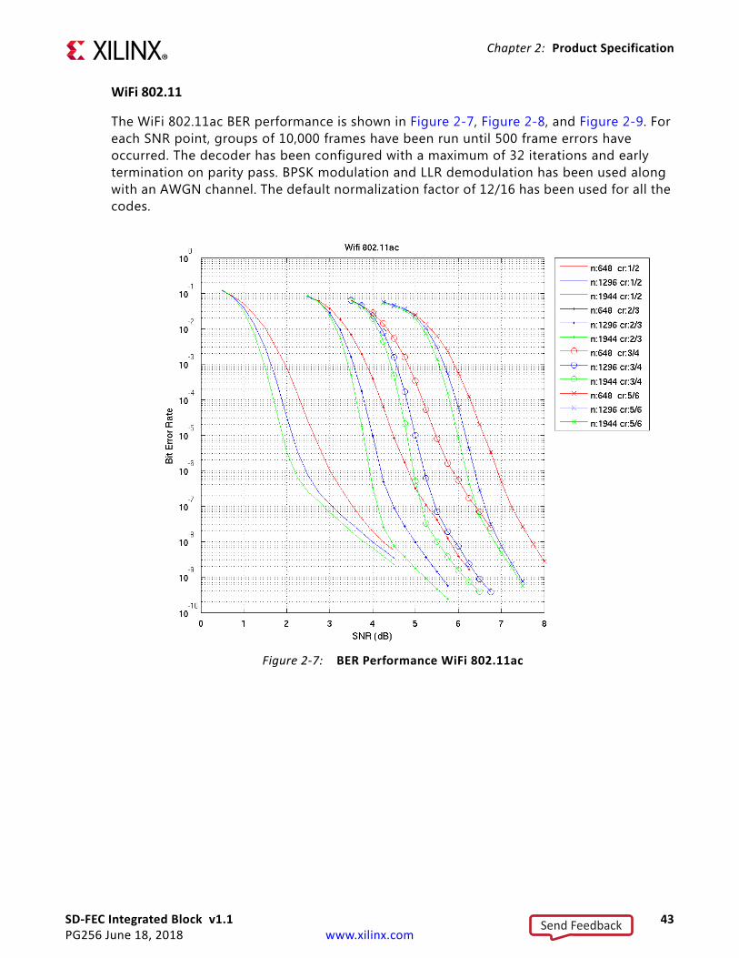
SD-FEC Integrated Block v1.1 43PG256 June 18, 2018 www.xilinx.com
Chapter 2: Product Specification
WiFi 802.11
The WiFi 802.11ac BER performance is shown in Figure 2-7, Figure 2-8, and Figure 2-9. For each SNR point, groups of 10,000 frames have been run until 500 frame errors have occurred. The decoder has been configured with a maximum of 32 iterations and early termination on parity pass. BPSK modulation and LLR demodulation has been used along with an AWGN channel. The default normalization factor of 12/16 has been used for all the codes.
X-Ref Target - Figure 2-7
Figure 2-7: BER Performance WiFi 802.11ac
Send Feedback
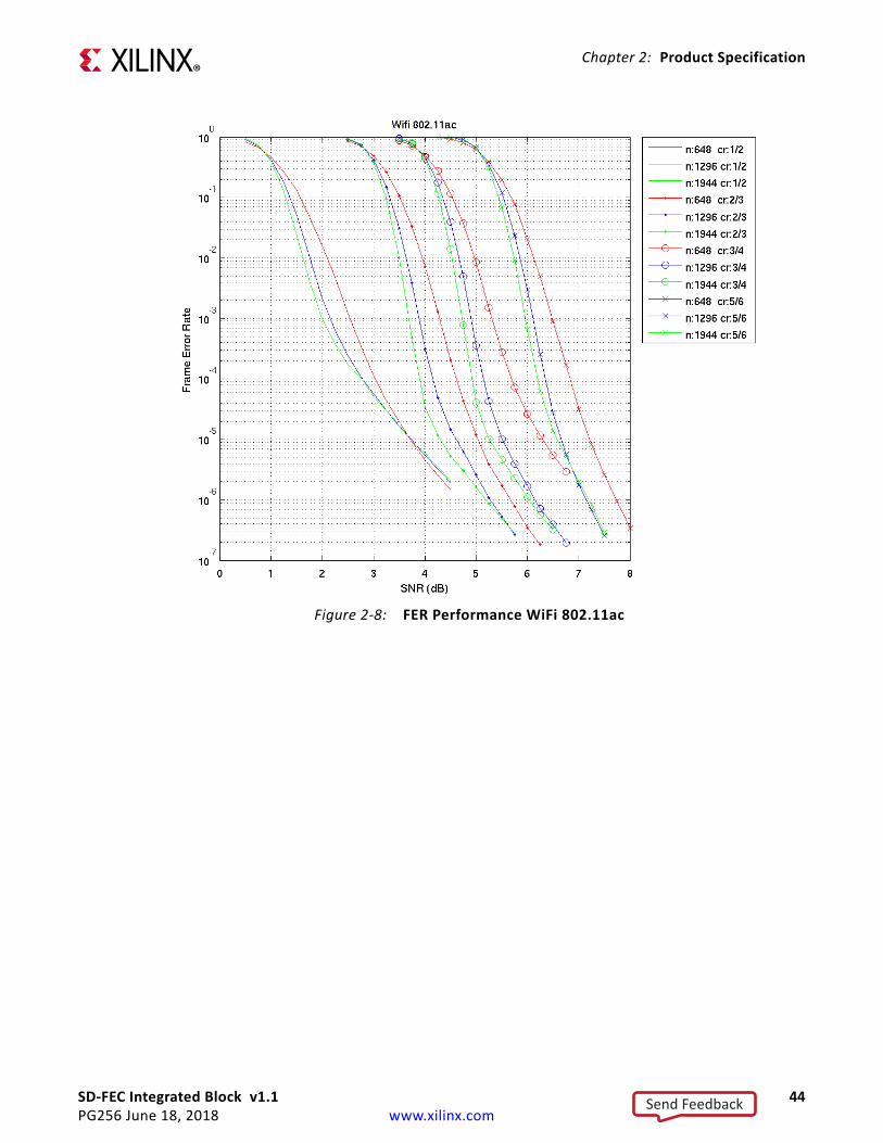
SD-FEC Integrated Block v1.1 44PG256 June 18, 2018 www.xilinx.com
Chapter 2: Product Specification
X-Ref Target - Figure 2-8
Figure 2-8: FER Performance WiFi 802.11ac
Send Feedback

SD-FEC Integrated Block v1.1 45PG256 June 18, 2018 www.xilinx.com
Chapter 2: Product Specification
X-Ref Target - Figure 2-9
Figure 2-9: Average Iterations WiFi 802.11ac
Send Feedback
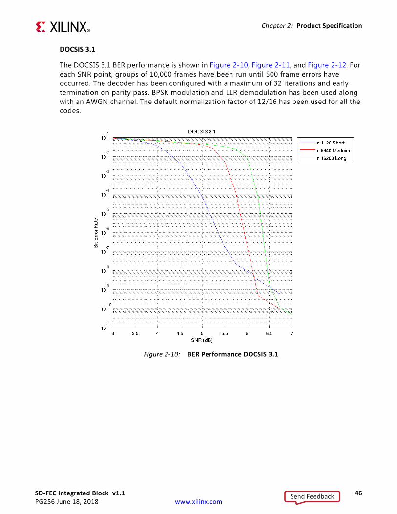
SD-FEC Integrated Block v1.1 46PG256 June 18, 2018 www.xilinx.com
Chapter 2: Product Specification
DOCSIS 3.1
The DOCSIS 3.1 BER performance is shown in Figure 2-10, Figure 2-11, and Figure 2-12. For each SNR point, groups of 10,000 frames have been run until 500 frame errors have occurred. The decoder has been configured with a maximum of 32 iterations and early termination on parity pass. BPSK modulation and LLR demodulation has been used along with an AWGN channel. The default normalization factor of 12/16 has been used for all the codes.
X-Ref Target - Figure 2-10
Figure 2-10: BER Performance DOCSIS 3.1
Send Feedback
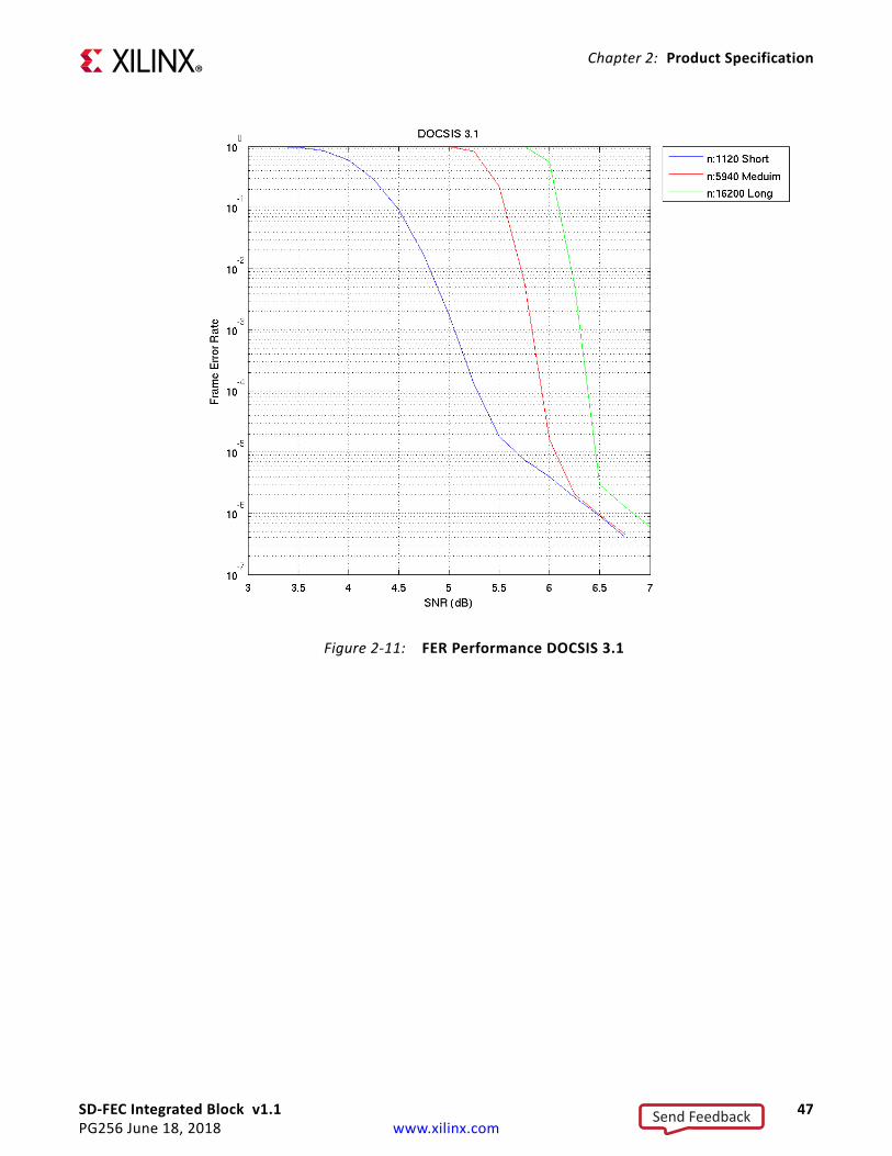
SD-FEC Integrated Block v1.1 47PG256 June 18, 2018 www.xilinx.com
Chapter 2: Product Specification
X-Ref Target - Figure 2-11
Figure 2-11: FER Performance DOCSIS 3.1
Send Feedback
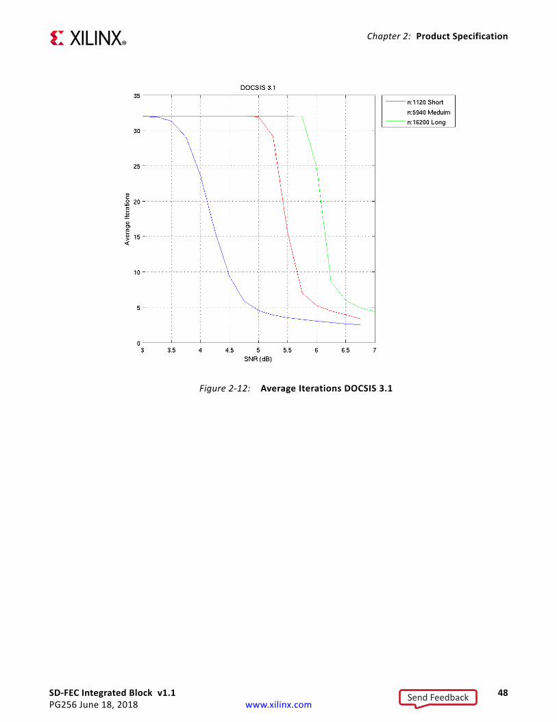
SD-FEC Integrated Block v1.1 48PG256 June 18, 2018 www.xilinx.com
Chapter 2: Product Specification
X-Ref Target - Figure 2-12
Figure 2-12: Average Iterations DOCSIS 3.1
Send Feedback
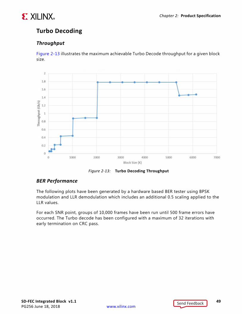
SD-FEC Integrated Block v1.1 49PG256 June 18, 2018 www.xilinx.com
Chapter 2: Product Specification
Turbo Decoding
Throughput
Figure 2-13 illustrates the maximum achievable Turbo Decode throughput for a given block size.
BER Performance
The following plots have been generated by a hardware based BER tester using BPSK modulation and LLR demodulation which includes an additional 0.5 scaling applied to the LLR values.
For each SNR point, groups of 10,000 frames have been run until 500 frame errors have occurred. The Turbo decode has been configured with a maximum of 32 iterations with early termination on CRC pass.
X-Ref Target - Figure 2-13
Figure 2-13: Turbo Decoding Throughput
Send Feedback

SD-FEC Integrated Block v1.1 50PG256 June 18, 2018 www.xilinx.com
Chapter 2: Product Specification
Max Scale (Scale Factor 0.75)
X-Ref Target - Figure 2-14
Figure 2-14: Turbo Decoding BER Performance - Max Scale
Send Feedback
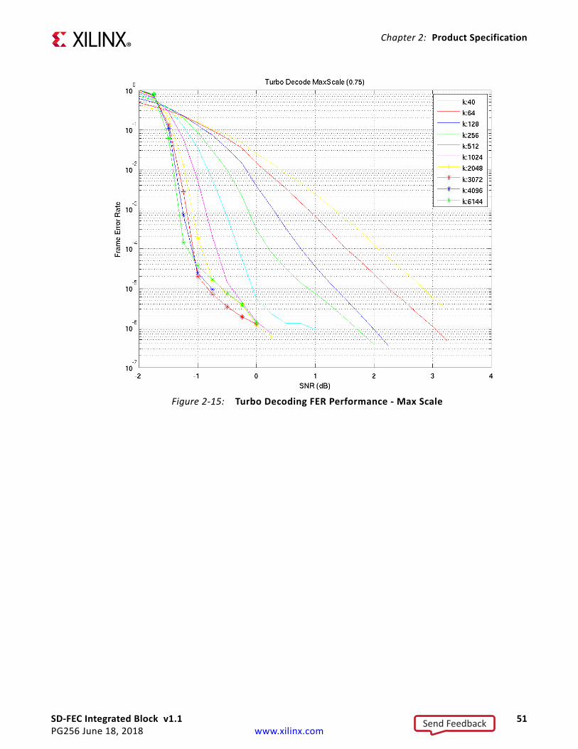
SD-FEC Integrated Block v1.1 51PG256 June 18, 2018 www.xilinx.com
Chapter 2: Product Specification
X-Ref Target - Figure 2-15
Figure 2-15: Turbo Decoding FER Performance - Max Scale
Send Feedback

SD-FEC Integrated Block v1.1 52PG256 June 18, 2018 www.xilinx.com
Chapter 2: Product Specification
X-Ref Target - Figure 2-16
Figure 2-16: Turbo Decoding Average Iterations - Max Scale
Send Feedback
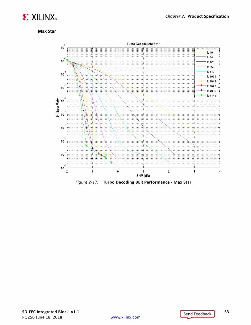
SD-FEC Integrated Block v1.1 53PG256 June 18, 2018 www.xilinx.com
Chapter 2: Product Specification
Max Star
X-Ref Target - Figure 2-17
Figure 2-17: Turbo Decoding BER Performance - Max Star
Send Feedback

SD-FEC Integrated Block v1.1 54PG256 June 18, 2018 www.xilinx.com
Chapter 2: Product Specification
X-Ref Target - Figure 2-18
Figure 2-18: Turbo Decoding FER Performance - Max Star
Send Feedback

SD-FEC Integrated Block v1.1 55PG256 June 18, 2018 www.xilinx.com
Chapter 2: Product Specification
Register SpaceIMPORTANT: Registers should be programmed through a device driver (this generates correct values from simple definitions of LDPC codes). The driver is provided by Xilinx.
The register map consists of the following types of parameters:
• Core Parameters (common to all codes)
• Turbo Code Parameters
• LDPC Code Parameters (per code)
• Shared LDPC Code Parameters
X-Ref Target - Figure 2-19
Figure 2-19: Turbo Decoding Average Iterations - Max Star
Send Feedback

SD-FEC Integrated Block v1.1 56PG256 June 18, 2018 www.xilinx.com
Chapter 2: Product Specification
All registers start on 32-bit word aligned addresses. The two LSBs of the read and write addresses are assumed to be zero.
Register read write access restrictions are summarized under the following sections. Further details of how code parameters might be managed are provided under Parameter Management.
Table 2-31: Register Space
Address (Hex) Register Name
__Core Parameters
0x00 AXI_WR_PROTECT Register (0x00)
0x04 CODE_WR_PROTECT Register (0x04)
0x08 ACTIVE Register (0x08)
0x0C AXIS_WIDTH Register (0x0C)
0x10 AXIS_ENABLE Register (0x10)
0x14 FEC_CODE Register (0x14)
0x18 ORDER Register (0x18)
0x1C Interrupt Status Register (ISR) (0x1C)
0x20 Interrupt Enable Register (IER) (0x20)
0x24 Interrupt Disable Register (IDR) (0x24)
0x28 Interrupt Mask Register (IMR) (0x28)
0x2C ECC Interrupt Status Register (0x2C)
0x30 ECC Interrupt Enable Register (0x30)
0x34 ECC Interrupt Disable Register (0x34)
0x38 ECC Interrupt Mask Register (0x38)
0x3C BYPASS Register (0x3C)
Turbo Code Parameters
0x100 Turbo Code Register (0x100)
LDPC Code Parameters
0x2000+CODE*0x10 REG0 Register (0x2000+CODE*0x10)(1)
0x2004+CODE*0x10 REG1 Register (0x2004+CODE*0x10)(1)
0x2008+CODE*0x10 REG2 Register (0x2008+CODE*0x10)(1)
0x200C+CODE*0x10 REG3 Register (0x200C+CODE*0x10)(1)
Shared LDPC Code Parameters
0x10000–0x103FC SC_TABLE Register (0x10000–0x103FC)
0x18000–0x18FFC LA_TABLE Register (0x18000–0x18FFC)
0x20000–0x27FFC QC_TABLE Register (0x20000–0x27FFC)
Send Feedback
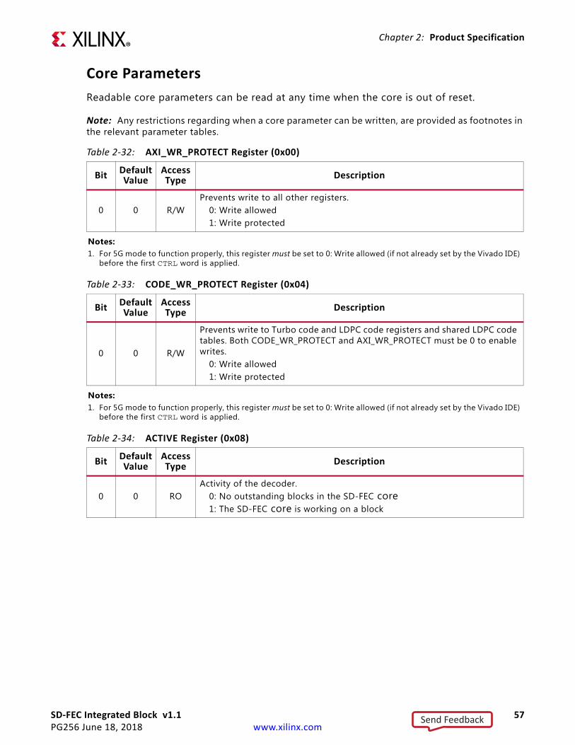
SD-FEC Integrated Block v1.1 57PG256 June 18, 2018 www.xilinx.com
Chapter 2: Product Specification
Core ParametersReadable core parameters can be read at any time when the core is out of reset.
Note: Any restrictions regarding when a core parameter can be written, are provided as footnotes in the relevant parameter tables.
Table 2-32: AXI_WR_PROTECT Register (0x00)
Bit DefaultValue
Access Type Description
0 0 R/WPrevents write to all other registers.
0: Write allowed1: Write protected
Notes: 1. For 5G mode to function properly, this register must be set to 0: Write allowed (if not already set by the Vivado IDE)
before the first CTRL word is applied.
Table 2-33: CODE_WR_PROTECT Register (0x04)
Bit DefaultValue
Access Type Description
0 0 R/W
Prevents write to Turbo code and LDPC code registers and shared LDPC code tables. Both CODE_WR_PROTECT and AXI_WR_PROTECT must be 0 to enable writes.
0: Write allowed1: Write protected
Notes: 1. For 5G mode to function properly, this register must be set to 0: Write allowed (if not already set by the Vivado IDE)
before the first CTRL word is applied.
Table 2-34: ACTIVE Register (0x08)
Bit DefaultValue
Access Type Description
0 0 ROActivity of the decoder.
0: No outstanding blocks in the SD-FEC core1: The SD-FEC core is working on a block
Send Feedback
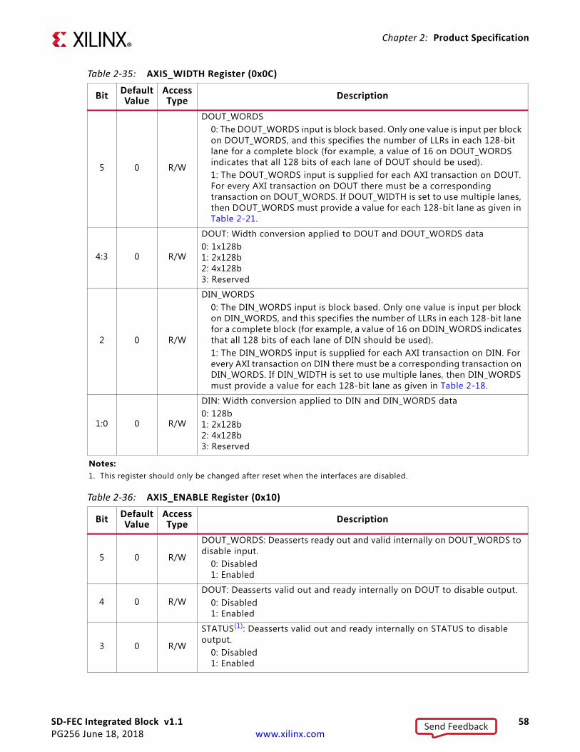
SD-FEC Integrated Block v1.1 58PG256 June 18, 2018 www.xilinx.com
Chapter 2: Product Specification
Table 2-35: AXIS_WIDTH Register (0x0C)
Bit DefaultValue
Access Type Description
5 0 R/W
DOUT_WORDS0: The DOUT_WORDS input is block based. Only one value is input per block on DOUT_WORDS, and this specifies the number of LLRs in each 128-bit lane for a complete block (for example, a value of 16 on DOUT_WORDS indicates that all 128 bits of each lane of DOUT should be used).1: The DOUT_WORDS input is supplied for each AXI transaction on DOUT. For every AXI transaction on DOUT there must be a corresponding transaction on DOUT_WORDS. If DOUT_WIDTH is set to use multiple lanes, then DOUT_WORDS must provide a value for each 128-bit lane as given in Table 2-21.
4:3 0 R/W
DOUT: Width conversion applied to DOUT and DOUT_WORDS data0: 1x128b1: 2x128b2: 4x128b3: Reserved
2 0 R/W
DIN_WORDS0: The DIN_WORDS input is block based. Only one value is input per block on DIN_WORDS, and this specifies the number of LLRs in each 128-bit lane for a complete block (for example, a value of 16 on DDIN_WORDS indicates that all 128 bits of each lane of DIN should be used).1: The DIN_WORDS input is supplied for each AXI transaction on DIN. For every AXI transaction on DIN there must be a corresponding transaction on DIN_WORDS. If DIN_WIDTH is set to use multiple lanes, then DIN_WORDS must provide a value for each 128-bit lane as given in Table 2-18.
1:0 0 R/W
DIN: Width conversion applied to DIN and DIN_WORDS data0: 128b1: 2x128b2: 4x128b3: Reserved
Notes: 1. This register should only be changed after reset when the interfaces are disabled.
Table 2-36: AXIS_ENABLE Register (0x10)
Bit DefaultValue
Access Type Description
5 0 R/W
DOUT_WORDS: Deasserts ready out and valid internally on DOUT_WORDS to disable input.
0: Disabled1: Enabled
4 0 R/WDOUT: Deasserts valid out and ready internally on DOUT to disable output.
0: Disabled1: Enabled
3 0 R/W
STATUS(1): Deasserts valid out and ready internally on STATUS to disable output.
0: Disabled1: Enabled
Send Feedback

SD-FEC Integrated Block v1.1 59PG256 June 18, 2018 www.xilinx.com
Chapter 2: Product Specification
2 0 R/W
DIN_WORDS: Deasserts ready out and valid internally on DIN_WORDS to disable input.
0: Disabled1: Enabled
1 0 R/WDIN: Deasserts ready out and valid internally on DIN to disable input.
0: Disabled1: Enabled
0 0 R/WCTRL(2): Deasserts ready out and valid internally on CTRL to disable input.
0: Disabled1: Enabled
Notes: 1. For 5G mode to function properly, STATUS must be set to Enabled (if not already set by the Vivado IDE) before the
first CTRL word is applied.2. For 5G mode to function properly, CTRL must be set to Enabled (if not already set by the Vivado IDE) before the
first CTRL word is applied.
Table 2-37: FEC_CODE Register (0x14)
Bit DefaultValue
Access Type Description
0 0 R/WFEC code to be used
0: Turbo code1: LDPC code
Notes: 1. This register should only be changed when the core is not active (ACTIVE is 0).
Table 2-38: ORDER Register (0x18)
Bit DefaultValue
Access Type Description
0 0 R/WSpecifies whether the order of blocks can change from input to output
0: Maintain order1: Out-of-order
Notes: 1. This register should only be changed when the core is not active (ACTIVE is 0).
Table 2-39: Interrupt Status Register (ISR) (0x1C)
Bit(1) DefaultValue
Access Type Description
5 0 R/W DOUT_WORDS tlast unexpected
4 0 R/W DOUT_WORDS tlast missing
3 0 R/W DIN_WORDS tlast unexpected
2 0 R/W DIN_WORDS tlast missing
1 0 R/W DIN tlast unexpected
Table 2-36: AXIS_ENABLE Register (0x10) (Cont’d)
Bit DefaultValue
Access Type Description
Send Feedback

SD-FEC Integrated Block v1.1 60PG256 June 18, 2018 www.xilinx.com
Chapter 2: Product Specification
0 0 R/W DIN tlast missing
Notes: 1. Write 1 to respective bit to clear.2. This register reflects the raw interrupt status and is not masked by the IMR.
Table 2-40: Interrupt Enable Register (IER) (0x20)
Bit(1) DefaultValue
Access Type Description
5 0 WO DOUT_WORDS tlast unexpected
4 0 WO DOUT_WORDS tlast missing
3 0 WO DIN_WORDS tlast unexpected
2 0 WO DIN_WORDS tlast missing
1 0 WO DIN tlast unexpected
0 0 WO DIN tlast missing
Notes: 1. Read 0. Write 1 to respective bit to enable interrupt (respective bit of IMR is set to 0). Write 0 ignored.
Table 2-41: Interrupt Disable Register (IDR) (0x24)
Bit(1) DefaultValue
Access Type Description
5 0 WO DOUT_WORDS tlast unexpected
4 0 WO DOUT_WORDS tlast missing
3 0 WO DIN_WORDS tlast unexpected
2 0 WO DIN_WORDS tlast missing
1 0 WO DIN tlast unexpected
0 0 WO DIN tlast missing
Notes: 1. Read 0. Write 1 to respective bit to disable interrupt (respective bit of IMR is set to 1). Write 0 ignored.
Table 2-42: Interrupt Mask Register (IMR) (0x28)
Bit DefaultValue
Access Type Description
5 1 RO DOUT_WORDS tlast unexpected
4 1 RO DOUT_WORDS tlast missing
3 1 RO DIN_WORDS tlast unexpected
2 1 RO DIN_WORDS tlast missing
1 1 RO DIN tlast unexpected
Table 2-39: Interrupt Status Register (ISR) (0x1C) (Cont’d)
Bit(1) DefaultValue
Access Type Description
Send Feedback

SD-FEC Integrated Block v1.1 61PG256 June 18, 2018 www.xilinx.com
Chapter 2: Product Specification
.
0 1 RO DIN tlast missing
Notes: 1. If mask bit is set, then interrupt is masked, that is, it does not cause the interrupt pin to go High.
Table 2-43: ECC Interrupt Status Register (0x2C)
Bit(1) DefaultValue
Access Type Description(2)
29 0 R/W LDPC REF NM_NMQC Table ECC two-bit error (5G NR mode)/LDPC CODE REG ECC two-bit error (Initialized non-5G mode)(3)(4)
28 0 R/W LDPC REF QC Table ECC two-bit error(3)(4)
27 0 R/W LDPC REF LA Table ECC two-bit error(3)(4)
26 0 R/W LDPC REF SC Table ECC two-bit error(3)(4)
25 0 R/W LDPC REF NM_NMQC Table ECC event (5G NR mode)/LDPC CODE REG ECC event (Initialized non-5G mode)(3)(5)
24 0 R/W LDPC REF QC Table ECC event(3)
23 0 R/W LDPC REF LA Table ECC event(3)
22 0 R/W LDPC REF SC Table ECC event(3)
21 0 R/W LDPC final parity calc memory ECC two-bit error(4)
20 0 R/W LDPC QC_TABLE memory 3 ECC two-bit error(4)
19 0 R/W LDPC QC_TABLE memory 2 ECC two-bit error(4)
18 0 R/W LDPC QC_TABLE memory 1 ECC two-bit error(4)
17 0 R/W LDPC QC_TABLE memory 0 ECC two-bit error(4)
16 0 R/W LDPC LA_TABLE memory ECC two-bit error(4)
15 0 R/W LDPC SC_TABLE memory ECC two-bit error(4)
14 0 R/W LDPC code REG3 memory ECC two-bit error(4)
13 0 R/W LDPC code REG2 memory ECC two-bit error(4)
12 0 R/W LDPC code REG1 memory ECC two-bit error(4)
11 0 R/W LDPC ode REG0 memory ECC two-bit error(4)
10 0 R/W LDPC final parity calc memory ECC event(5)
9 0 R/W LDPC QC_TABLE memory 3 ECC event
8 0 R/W LDPC QC_TABLE memory 2 ECC event
7 0 R/W LDPC QC_TABLE memory 1 ECC event
6 0 R/W LDPC QC_TABLE memory 0 ECC event
5 0 R/W LDPC LA_TABLE memory ECC event
4 0 R/W LDPC SC_TABLE memory ECC event
3 0 R/W LDPC code REG3 memory ECC event
Table 2-42: Interrupt Mask Register (IMR) (0x28) (Cont’d)
Bit DefaultValue
Access Type Description
Send Feedback

SD-FEC Integrated Block v1.1 62PG256 June 18, 2018 www.xilinx.com
Chapter 2: Product Specification
2 0 R/W LDPC code REG2 memory ECC event
1 0 R/W LDPC code REG1 memory ECC event
0 0 R/W LDPC code REG0 memory ECC event
Notes: 1. Write 1 to respective bit to clear.2. This register reflects the raw interrupt status and is not masked by the IMR.3. These memories exist in the SD-FEC support logic in 5G NR and initialized non-5G modes.4. The ECC two-bit error register is set when two errors are detected in a word read from the respective memory. It
can also be set when the number of errors in a word is greater than two—however, this is not guaranteed. Uncorrected multi-bit errors can result in incorrect core behavior.
5. An ECC event is when one or more errors have been detected in a word read from the respective memory. If present without an ECC two-bit error then only a single error has been detected, which has been corrected.
Table 2-44: ECC Interrupt Enable Register (0x30)
Bit(1) DefaultValue
Access Type Description
29 0 WO LDPC REF NM_NMQC Table ECC two-bit error (5G NR mode)/LDPC CODE REG ECC two-bit error (Initialized non-5G mode)(2)(3)
28 0 WO LDPC REF QC Table ECC two-bit error(2)(3)
27 0 WO LDPC REF LA Table ECC two-bit error(2)(3)
26 0 WO LDPC REF SC Table ECC two-bit error(2)(3)
25 0 WO LDPC REF NM_NMQC Table ECC event (5G NR mode)/LDPC CODE REG ECC event (Initialized non-5G mode)(2)(3)
24 0 WO LDPC REF QC Table ECC event(2)
23 0 WO LDPC REF LA Table ECC event(2)
22 0 WO LDPC REF SC Table ECC event(2)
21 0 WO LDPC final parity calc memory ECC two-bit error(3)
20 0 WO LDPC QC_TABLE memory 3 ECC two-bit error(3)
19 0 WO LDPC QC_TABLE memory 2 ECC two-bit error(3)
18 0 WO LDPC QC_TABLE memory 1 ECC two-bit error(3)
17 0 WO LDPC QC_TABLE memory 0 ECC two-bit error(3)
16 0 WO LDPC LA_TABLE memory ECC two-bit error(3)
15 0 WO LDPC SC_TABLE memory ECC two-bit error(3)
14 0 WO LDPC code REG3 memory ECC two-bit error(3)
13 0 WO LDPC code REG2 memory ECC two-bit error(3)
12 0 WO LDPC code REG1 memory ECC two-bit error(3)
11 0 WO LDPC code REG0 memory ECC two-bit error(3)
10 0 WO LDPC final parity calc memory ECC event(4)
Table 2-43: ECC Interrupt Status Register (0x2C) (Cont’d)
Bit(1) DefaultValue
Access Type Description(2)
Send Feedback
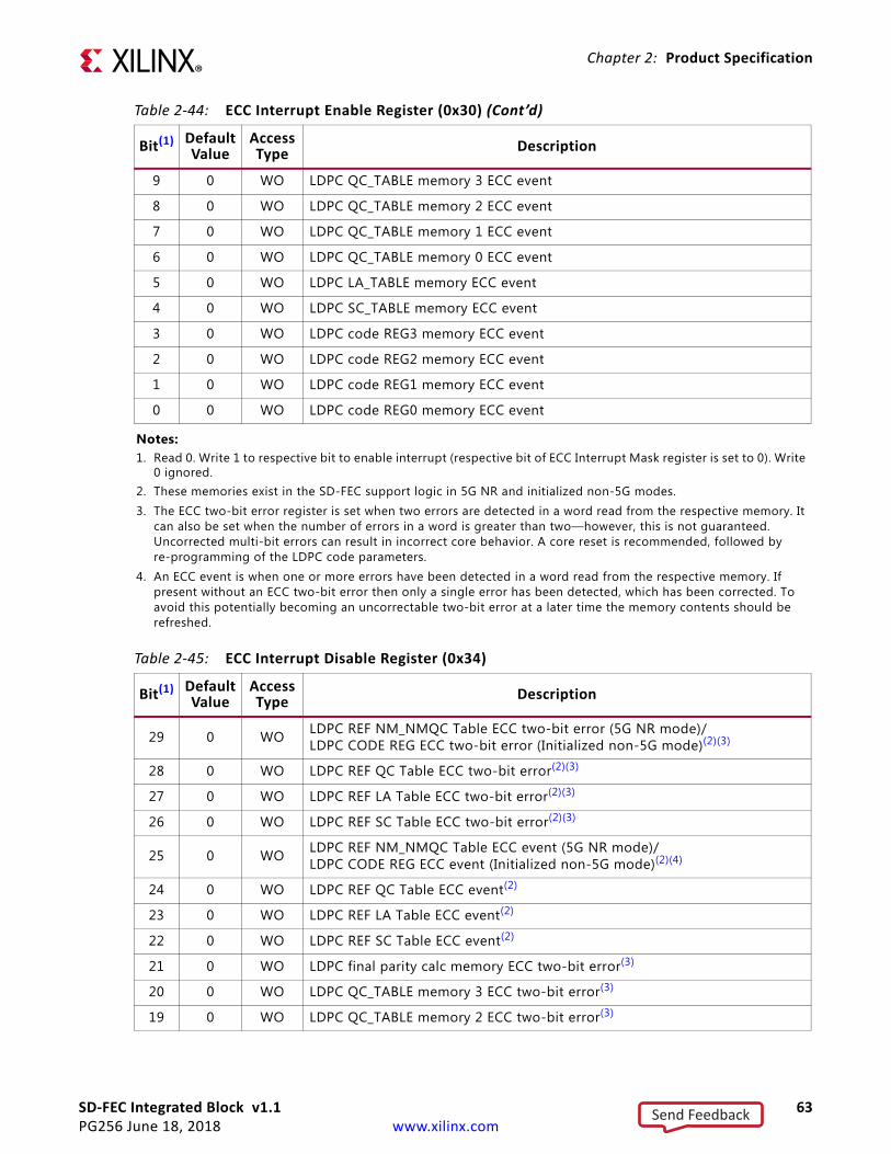
SD-FEC Integrated Block v1.1 63PG256 June 18, 2018 www.xilinx.com
Chapter 2: Product Specification
9 0 WO LDPC QC_TABLE memory 3 ECC event
8 0 WO LDPC QC_TABLE memory 2 ECC event
7 0 WO LDPC QC_TABLE memory 1 ECC event
6 0 WO LDPC QC_TABLE memory 0 ECC event
5 0 WO LDPC LA_TABLE memory ECC event
4 0 WO LDPC SC_TABLE memory ECC event
3 0 WO LDPC code REG3 memory ECC event
2 0 WO LDPC code REG2 memory ECC event
1 0 WO LDPC code REG1 memory ECC event
0 0 WO LDPC code REG0 memory ECC event
Notes: 1. Read 0. Write 1 to respective bit to enable interrupt (respective bit of ECC Interrupt Mask register is set to 0). Write
0 ignored.2. These memories exist in the SD-FEC support logic in 5G NR and initialized non-5G modes.3. The ECC two-bit error register is set when two errors are detected in a word read from the respective memory. It
can also be set when the number of errors in a word is greater than two—however, this is not guaranteed. Uncorrected multi-bit errors can result in incorrect core behavior. A core reset is recommended, followed by re-programming of the LDPC code parameters.
4. An ECC event is when one or more errors have been detected in a word read from the respective memory. If present without an ECC two-bit error then only a single error has been detected, which has been corrected. To avoid this potentially becoming an uncorrectable two-bit error at a later time the memory contents should be refreshed.
Table 2-45: ECC Interrupt Disable Register (0x34)
Bit(1) DefaultValue
Access Type Description
29 0 WO LDPC REF NM_NMQC Table ECC two-bit error (5G NR mode)/LDPC CODE REG ECC two-bit error (Initialized non-5G mode)(2)(3)
28 0 WO LDPC REF QC Table ECC two-bit error(2)(3)
27 0 WO LDPC REF LA Table ECC two-bit error(2)(3)
26 0 WO LDPC REF SC Table ECC two-bit error(2)(3)
25 0 WO LDPC REF NM_NMQC Table ECC event (5G NR mode)/LDPC CODE REG ECC event (Initialized non-5G mode)(2)(4)
24 0 WO LDPC REF QC Table ECC event(2)
23 0 WO LDPC REF LA Table ECC event(2)
22 0 WO LDPC REF SC Table ECC event(2)
21 0 WO LDPC final parity calc memory ECC two-bit error(3)
20 0 WO LDPC QC_TABLE memory 3 ECC two-bit error(3)
19 0 WO LDPC QC_TABLE memory 2 ECC two-bit error(3)
Table 2-44: ECC Interrupt Enable Register (0x30) (Cont’d)
Bit(1) DefaultValue
Access Type Description
Send Feedback

SD-FEC Integrated Block v1.1 64PG256 June 18, 2018 www.xilinx.com
Chapter 2: Product Specification
18 0 WO LDPC QC_TABLE memory 1 ECC two-bit error(3)
17 0 WO LDPC QC_TABLE memory 0 ECC two-bit error(3)
16 0 WO LDPC LA_TABLE memory ECC two-bit error(3)
15 0 WO LDPC SC_TABLE memory ECC two-bit error(3)
14 0 WO LDPC code REG3 memory ECC two-bit error(3)
13 0 WO LDPC code REG2 memory ECC two-bit error(3)
12 0 WO LDPC code REG1 memory ECC two-bit error(3)
11 0 WO LDPC code REG0 memory ECC two-bit error(3)
10 0 WO LDPC final parity calc memory ECC event(4)
9 0 WO LDPC QC_TABLE memory 3 ECC event
8 0 WO LDPC QC_TABLE memory 2 ECC event
7 0 WO LDPC QC_TABLE memory 1 ECC event
6 0 WO LDPC QC_TABLE memory 0 ECC event
5 0 WO LDPC LA_TABLE memory ECC event
4 0 WO LDPC SC_TABLE memory ECC event
3 0 WO LDPC code REG3 memory ECC event
2 0 WO LDPC code REG2 memory ECC event
1 0 WO LDPC code REG1 memory ECC event
0 0 WO LDPC code REG0 memory ECC event
Notes: 1. Read 0. Write 1 to respective bit to disable interrupt (respective bit of ECC Interrupt Mask register is set to 1). Write
0 ignored.2. These memories exist in the SD-FEC support logic in 5G NR and initialized non-5G modes.3. The ECC two-bit error register is set when two errors are detected in a word read from the respective memory. It
can also be set when the number of errors in a word is greater than two—however, this is not guaranteed. Uncorrected multi-bit errors can result in incorrect core behavior. A core reset is recommended, followed by re-programming of the LDPC code parameters.
4. An ECC event is when one or more errors have been detected in a word read from the respective memory. If present without an ECC two-bit error then only a single error has been detected, which has been corrected. To avoid this potentially becoming an uncorrectable two-bit error at a later time the memory contents should be refreshed.
Table 2-45: ECC Interrupt Disable Register (0x34) (Cont’d)
Bit(1) DefaultValue
Access Type Description
Send Feedback

SD-FEC Integrated Block v1.1 65PG256 June 18, 2018 www.xilinx.com
Chapter 2: Product Specification
Table 2-46: ECC Interrupt Mask Register (0x38)
Bit(1) DefaultValue
Access Type Description
29 0 RO LDPC REF NM_NMQC Table ECC two-bit error (5G NR mode)/LDPC CODE REG ECC two-bit error (Initialized non-5G mode)(2)(3)
28 0 RO LDPC REF QC Table ECC two-bit error(2)(3)
27 0 RO LDPC REF LA Table ECC two-bit error(2)(3)
26 0 RO LDPC REF SC Table ECC two-bit error(2)(3)
25 0 RO LDPC REF NM_NMQC Table ECC event (5G NR mode)/LDPC CODE REG ECC event (Initialized non-5G mode)(2)(4)
24 0 RO LDPC REF QC Table ECC event(2)
23 0 RO LDPC REF LA Table ECC event(2)
22 0 RO LDPC REF SC Table ECC event(2)
21 1 RO LDPC final parity calc memory ECC two-bit error(3)
20 1 RO LDPC QC_TABLE memory 3 ECC two-bit error(3)
19 1 RO LDPC QC_TABLE memory 2 ECC two-bit error(3)
18 1 RO LDPC QC_TABLE memory 1 ECC two-bit error(3)
17 1 RO LDPC QC_TABLE memory 0 ECC two-bit error(3)
16 1 RO LDPC LA_TABLE memory ECC two-bit error(3)
15 1 RO LDPC SC_TABLE memory ECC two-bit error(3)
14 1 RO LDPC code REG3 memory ECC two-bit error(3)
13 1 RO LDPC code REG2 memory ECC two-bit error(3)
12 1 RO LDPC code REG1 memory ECC two-bit error(3)
11 1 RO LDPC code REG0 memory ECC two-bit error(3)
10 1 RO LDPC final parity calc memory ECC event(4)
9 1 RO LDPC QC_TABLE memory 3 ECC event
8 1 RO LDPC QC_TABLE memory 2 ECC event
7 1 RO LDPC QC_TABLE memory 1 ECC event
6 1 RO LDPC QC_TABLE memory 0 ECC event
5 1 RO LDPC LA_TABLE memory ECC event
4 1 RO LDPC SC_TABLE memory ECC event
Send Feedback

SD-FEC Integrated Block v1.1 66PG256 June 18, 2018 www.xilinx.com
Chapter 2: Product Specification
Turbo Code ParametersIf the core is out of reset, Turbo code parameters can be read at any time. Turbo code parameters should only be updated when the core is not active (ACTIVE is 0).
3 1 RO LDPC code REG3 memory ECC event
2 1 RO LDPC code REG2 memory ECC event
1 1 RO LDPC code REG1 memory ECC event
0 1 RO LDPC code REG0 memory ECC event
Notes: 1. If mask bit is set, then interrupt is masked, that is, it does not cause the interrupt pin to go High.2. These memories exist in the SD-FEC support logic in 5G NR and initialized non-5G modes.3. The ECC two-bit error register is set when two errors are detected in a word read from the respective memory. It
can also be set when the number of errors in a word is greater than two—however, this is not guaranteed. Uncorrected multi-bit errors can result in incorrect core behavior. A core reset is recommended, followed by re-programming of the LDPC code parameters.
4. An ECC event is when one or more errors have been detected in a word read from the respective memory. If present without an ECC two-bit error then only a single error has been detected, which has been corrected. To avoid this potentially becoming an uncorrectable two-bit error at a later time the memory contents should be refreshed.
Table 2-47: BYPASS Register (0x3C)
Bit DefaultValue
Access Type Description
0 0 R/W
Perform function with given number of iterations (early termination not supported, so associated termination bits must be set to zero in CTRL input while BYPASS is set), but output is same as input (minus tail bits for Turbo decode) accounting for any soft to hard conversion.Parity pass/CRC flag is based on input values:
0: Normal operation1: Output same as input
Notes: 1. This register should only be changed when the core is not active (ACTIVE is 0).
Table 2-48: Turbo Code Register (0x100)
Bit DefaultValue
Access Type Description
11:8 0xC R/WSCALE_FACTOR
0: Scale=11-15: Scale = 0.0625*Scale
0 0 R/WALG: Turbo Decode Algorithm
0: Max_scale1: Max star
Table 2-46: ECC Interrupt Mask Register (0x38) (Cont’d)
Bit(1) DefaultValue
Access Type Description
Send Feedback
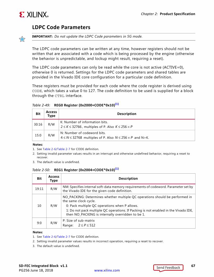
SD-FEC Integrated Block v1.1 67PG256 June 18, 2018 www.xilinx.com
Chapter 2: Product Specification
LDPC Code ParametersIMPORTANT: Do not update the LDPC Code parameters in 5G mode.
The LDPC code parameters can be written at any time, however registers should not be written that are associated with a code which is being processed by the engine (otherwise the behavior is unpredictable, and lockup might result, requiring a reset).
The LDPC code parameters can only be read while the core is not active (ACTIVE=0), otherwise 0 is returned. Settings for the LDPC code parameters and shared tables are provided in the Vivado IDE core configuration for a particular code definition.
These registers must be provided for each code where the code register is derived using CODE, which takes a value 0 to 127. The code definition to be used is supplied for a block through the CTRL interface.
Table 2-49: REG0 Register (0x2000+CODE*0x10)(1)
Bit Access Type Description
30:16 R/WK: Number of information bits.
, multiples of P. Also
15:0 R/WN: Number of codeword bits.
multiples of P. Also and N>K.
Notes: 1. See Table 2-6/Table 2-7 for CODE definition.2. Setting invalid parameter values results in an interrupt and otherwise undefined behavior, requiring a reset to
recover.3. The default value is undefined.
Table 2-50: REG1 Register (0x2004+CODE*0x10)(1)
Bit Access Type Description
19:11 R/W NM: Specifies internal soft-data memory requirements of codeword. Parameter set by the Vivado IDE for the given code definition.
10 R/W
NO_PACKING: Determines whether multiple QC operations should be performed in the same clock cycle.
0: Pack multiple QC operations when P allows.1: Do not pack multiple QC operations. If Packing is not enabled in the Vivado IDE, then NO_PACKING is internally overridden to be 1.
9:0 R/WP: Size of sub-matrixRange:
Notes: 1. See Table 2-6/Table 2-7 for CODE definition.2. Setting invalid parameter values results in incorrect operation, requiring a reset to recover.3. The default value is undefined.
2 K 32766≤ ≤ K 256 P×≤
4 N 32768≤ ≤ N 256 P×≤
2 P 512≤ ≤
Send Feedback
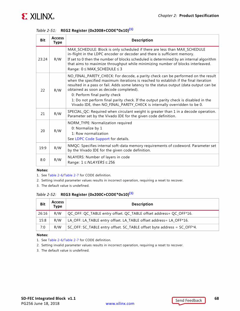
SD-FEC Integrated Block v1.1 68PG256 June 18, 2018 www.xilinx.com
Chapter 2: Product Specification
Table 2-51: REG2 Register (0x2008+CODE*0x10)(1)
Bit Access Type Description
23:24 R/W
MAX_SCHEDULE: Block is only scheduled if there are less than MAX_SCHEDULE in-flight in the LDPC encoder or decoder and there is sufficient memory.If set to 0 then the number of blocks scheduled is determined by an internal algorithm that aims to maximize throughput while minimizing number of blocks interleaved.Range:
22 R/W
NO_FINAL_PARITY_CHECK: For decode, a parity check can be performed on the result when the specified maximum iterations is reached to establish if the final iteration resulted in a pass or fail. Adds some latency to the status output (data output can be obtained as soon as decode completed).
0: Perform final parity check1: Do not perform final parity check. If the output parity check is disabled in the Vivado IDE, then NO_FINAL_PARITY_CHECK is internally overridden to be 0.
21 R/W SPECIAL_QC: Required when circulant weight is greater than 1 in a decode operation. Parameter set by the Vivado IDE for the given code definition.
20 R/W
NORM_TYPE: Normalization required0: Normalize by 11: Row normalization
See LDPC Code Support for details.
19:9 R/W NMQC: Specifies internal soft-data memory requirements of codeword. Parameter set by the Vivado IDE for the given code definition.
8:0 R/WNLAYERS: Number of layers in codeRange:
Notes: 1. See Table 2-6/Table 2-7 for CODE definition.2. Setting invalid parameter values results in incorrect operation, requiring a reset to recover.3. The default value is undefined.
Table 2-52: REG3 Register (0x200C+CODE*0x10)(1)
Bit Access Type Description
26:16 R/W QC_OFF: QC_TABLE entry offset. QC_TABLE offset address= QC_OFF*16.
15:8 R/W LA_OFF: LA_TABLE entry offset. LA_TABLE offset address= LA_OFF*16.
7:0 R/W SC_OFF: SC_TABLE entry offset. SC_TABLE offset byte address = SC_OFF*4.
Notes: 1. See Table 2-6/Table 2-7 for CODE definition.2. Setting invalid parameter values results in incorrect operation, requiring a reset to recover.3. The default value is undefined.
0 MAX_SCHEDULE 3≤ ≤
1 NLAYERS 256≤ ≤
Send Feedback

SD-FEC Integrated Block v1.1 69PG256 June 18, 2018 www.xilinx.com
Chapter 2: Product Specification
Shared LDPC Code ParametersIMPORTANT: Do not update the Shared LDPC Code parameters in 5G mode.
Table 2-53 to Table 2-55 are shared between LDPC codes. The offset pointers defined under the per-code parameters provide the start address of the required LDPC code information. The number of entries in the table required by a code depends on the other per-code parameters. The table addresses wrap (that is, a code can start at the top of a table and continue at the start address of each table).
Shared LDPC code parameters not in use by a code can be written. Writing to parameters in use can lead to unpredictable behavior, such as lock-up, requiring a reset to recover. The shared LDPC code parameters can only be read while the core is inactive (ACTIVE=0), otherwise 0 is returned.
Table 2-53 shows the normalization factors for the LDPC code.
Table 2-54 shows the parameters relating to each layer of the code.
Table 2-53: SC_TABLE Register (0x10000–0x103FC)
Bit Access Type Description
15:0 R/WFour packed 4-bit scale factors - one per layer.See LDPC Code Support for details.
Notes: 1. Read only possible while core is inactive (ACTIVE=0).2. The default value is undefined.
Table 2-54: LA_TABLE Register (0x18000–0x18FFC)
Bit Access Type Description
15:8 R/W Number of cycles to wait at start of layer to enforce data dependences. Parameter set by the Vivado IDE for the given code definition.
7 R/W Employed when circulant weight is greater than 1 in a decode operation. Parameter set by the Vivado IDE for the given code definition.
6:0 R/W Number of cycles per layer minus 1. Parameter set by the Vivado IDE for the given code definition. Depends upon packing factor (and so associated PSIZE).
Notes: 1. Read only possible while core is inactive (ACTIVE=0).2. The default value is undefined.
Send Feedback
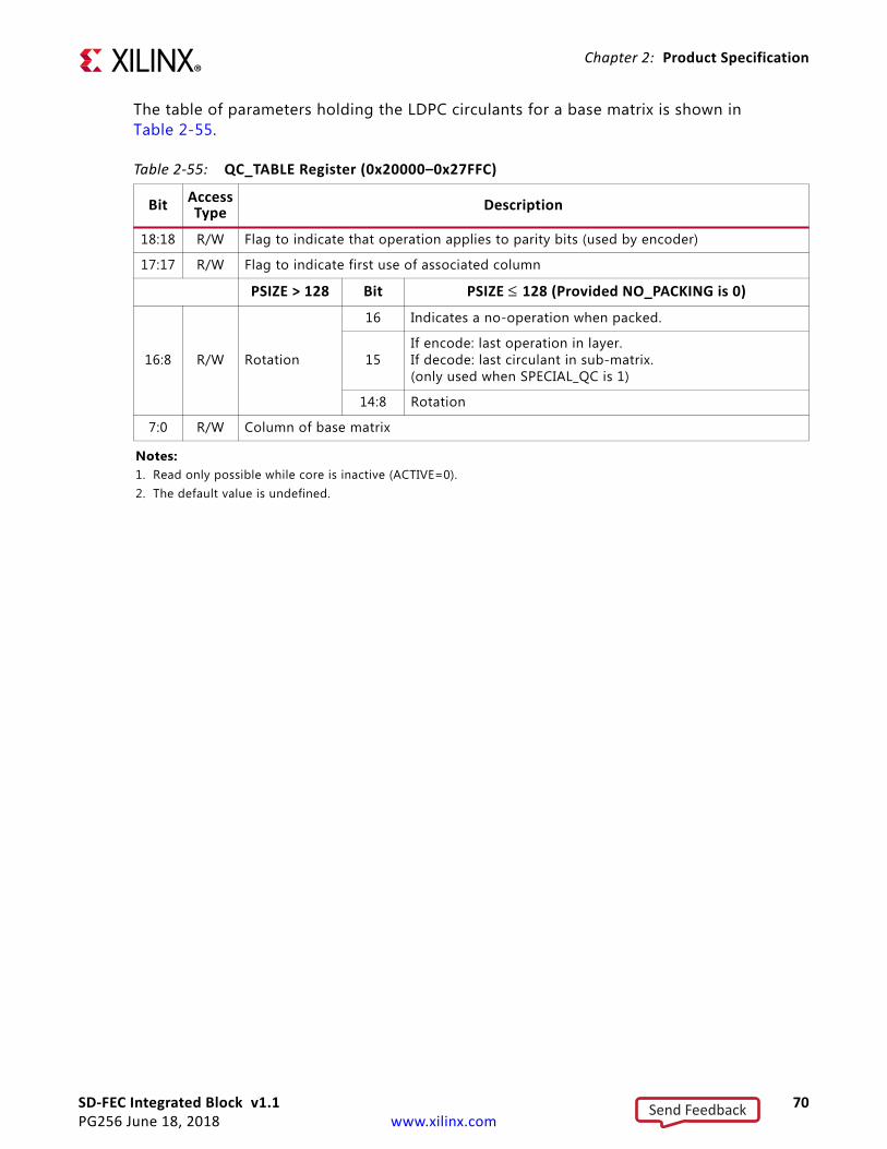
SD-FEC Integrated Block v1.1 70PG256 June 18, 2018 www.xilinx.com
Chapter 2: Product Specification
The table of parameters holding the LDPC circulants for a base matrix is shown in Table 2-55.
Table 2-55: QC_TABLE Register (0x20000–0x27FFC)
Bit Access Type Description
18:18 R/W Flag to indicate that operation applies to parity bits (used by encoder)
17:17 R/W Flag to indicate first use of associated column
PSIZE > 128 Bit PSIZE ≤ 128 (Provided NO_PACKING is 0)
16:8 R/W Rotation
16 Indicates a no-operation when packed.
15If encode: last operation in layer. If decode: last circulant in sub-matrix.(only used when SPECIAL_QC is 1)
14:8 Rotation
7:0 R/W Column of base matrix
Notes: 1. Read only possible while core is inactive (ACTIVE=0).2. The default value is undefined.
Send Feedback

SD-FEC Integrated Block v1.1 71PG256 June 18, 2018 www.xilinx.com
Chapter 3
Designing with the CoreThis chapter includes guidelines and additional information to facilitate designing with the core.
ClockingThe SD-FEC block operates from a separate clock to the programmable logic (PL), allowing the core to run at higher frequency.
Each interface has its own clock and clock domain crossing circuits to enable transfer of data over the interface. Certain interfaces also have width conversion to allow data bandwidth to be maintained with lower interface clock frequency.
See the Zynq UltraScale+ RFSoC Data Sheet: Overview (DS889) for the maximum frequency of core and interface clocks. Lower frequencies can be used.
Note that if the throughput and latency are limited by processing within the core, rather than by input/output, then the throughput is proportional to the core clock frequency. As such, if the core clock rate is reduced over the maximum value, there is a proportional reduction in throughput and an increase in latency relative to the maximum achievable. For example, if a 650 MHz clock is used rather than a 667 MHz clock, then the throughput at 650 MHz relative to the peak at 667 MHz is 650/667=0.975 times the peak throughput. Therefore, if the peak throughput at 667 MHz is 1 Gb/s, then the throughput at 650 MHz is 0.975G b/s.
ResetsA single active-Low reset signal, reset_n, is used to reset the core and its interfaces. Reset is applied asynchronously, and internal synchronizers ensure that the reset is deasserted synchronously in each domain. A reset is required after power-up. The application of reset causes the Core Parameters and Turbo Code Parameters registers to take their reset value (LDPC and Shared LDPC code parameters are undefined). In-flight blocks are discarded, and the core becomes inactive, with the interfaces synchronously entering their disabled state (AXIS_ENABLE is zero).
Send Feedback

SD-FEC Integrated Block v1.1 72PG256 June 18, 2018 www.xilinx.com
Chapter 3: Designing with the Core
The core comes out of reset with the AXI4-Stream interfaces disabled, allowing the interface width to be changed and code parameters to be written over the AXI4-Lite interface before operation begins. The final write can enable the interfaces to commence operation.
InterruptA single interrupt output signal indicates a number of error conditions. These conditions are defined by the Interrupt and ECC Interrupt Registers. Error conditions include:
• tlast missing on master interfaces: This is where a tlast input is not asserted on the last transfer relating to a block.
• tlast unexpected: This is when a tlast input is asserted unexpectedly (on all but the last transfer in a block).
These are described further in Use of TLAST. If these errors occur, then the SD-FEC core and connected circuits have to be reset to re-synchronize block transfer. Note that a reset of the SD-FEC core causes the Core Parameters registers to be reset (which includes disabling of the interfaces) and these registers have to be re-loaded (incurring a small number of cycles).
• Errors detected in ECC protected memory when a word is read through the AXI4-Lite interface, or by the LDPC decoder, when the latter is active. Both correctable single bit errors and uncorrectable two-bit errors are flagged (the latter might also include situations where there are more than two errors, but only detection of two-bit errors is guaranteed). Possible responses to each of these errors are summarized in Table 3-1.
Summary of Interrupt ResponsesPotential interrupt responses are summarized in Table 3-1.
Table 3-1: Error Detection/Correction and Reporting
ModePL Initialization Logic SD-FEC
ECC 1-Bit(If Enabled) ECC 2-Bit ECC 1-bit
(If Enabled) ECC 2-Bit Tlast Errors
Initialized retain I/F (LDPC code initialization and AXI4-lite interface present)
Inspect ECC ISR,bits 22 to 29 - Ignore or PL Reconfigure
Inspect ECC ISR,bits 26 to 29 -PL Reconfigure
Inspect ECC ISR, bits 0 to 21 -
Ignore or Reset
Inspect ECC ISR, bits 11 to 21 -
Reset
Inspect ISR -Reset
Initialized(LDPC code initialized andAXI4-Lite interface not present)
PL Reconfigure
PL Reconfigure
PL Reconfigure
PL Reconfigure
PL Reconfigure
Runtime Configured(LDPC code not initialized and AXI4-Lite interface present)
N/A N/A
Inspect ECC ISR, bits 0 to 21 -
Ignore orReprogramcodes when
inactive
Inspect ECC ISR,bits 11 to 21 -
Reset andReprogram
codes
Inspect ISR -Reset and
Reprogramcodes
Send Feedback

SD-FEC Integrated Block v1.1 73PG256 June 18, 2018 www.xilinx.com
Chapter 3: Designing with the Core
InterfacesAll interfaces on the Soft-Decision FEC block have clock-domain-crossing (CDC) FIFOs. The FIFO depths are given in Table 3-2. While the inner core enforces the DIN/DOUT_WORDS dependencies, the FIFOs can fill such that a number of transfers up to the FIFO depth can occur into DIN before being blocked by a lack of transfers on DIN_WORDS. In particular, this should be noted if interfaces are being disabled for some reason, the data in the FIFOs is still processed.
Parameter ManagementParameters should be carefully managed due to the wide variety of modes that is supported by the SD-FEC core. For 5G NR and initialized non-5G, the support logic takes control of the shared LDPC code parameters; therefore these parameters must not be, under any circumstances, written from the exposed AXI4-Lite interface provided. For 5G NR, the support logic also assumes that the AXI_WR_PROTECT and CODE_WR_PROTECT registers are writeable and CTRL and STATUS interfaces are enabled in the AXI_ENABLE register. If the interfaces are disabled after the first CTRL data is applied, the behavior is unpredictable. All other interfaces are disabled after reset and should be enabled prior to using the core.
In all other modes, all SD-FEC core interfaces are disabled from reset. This allows the opportunity to configure parameters (such as LDPC codes) prior to the interfaces being enabled. WR_PROTECT can then be enabled to prevent registers being changed during operation. If it is necessary to change codes during operation, it is recommended that an external circuit be used to prevent changing of codes that are in use, as the behavior of the core in this circumstance is undefined.
It is also possible to stop operation of the decoder by disabling the CTRL interface, and monitoring the ACTIVE register. Codes can then be changed without any risk of them being used. When code download is complete, the CTRL interface can be re-enabled.
IMPORTANT: Codes in use should not be updated. If codes in use are modified, the results are unpredictable.
Table 3-2: Depth of Interface CDC FIFOs
ChannelFIFO Depth
(For Given Interface Width Setting)
1 Lane 2 Lanes 4 Lanes
DIN, DIN_WORDS, DOUT, DOUT_WORDS 25 transfers 13 transfers 7 transfers
CTRL, STATUS 13 transfers in 5G mode, 6 transfers otherwise
Send Feedback

SD-FEC Integrated Block v1.1 74PG256 June 18, 2018 www.xilinx.com
Chapter 3: Designing with the Core
LDPC Code Support
LDPC Code OverviewLDPC codes are programmable through an AXI4-Lite interface. A class of Quasi-Cyclic (QC) codes are supported. Figure 3-1 elaborates the code parameterization and Table 3-3 summarizes the flexibility.
The checknode degree (DC) and variable node degree (DV) are counts of the number of 1s in each row and column respectively of the H matrix. For the respective base matrix, if sub-matrices have circulant weight greater than one, then DC and DV are counts of the total number of circulants in a layer or column respectively.
X-Ref Target - Figure 3-1
Figure 3-1: LDPC Quasi-Cyclic (QC) Code Structure
Table 3-3: LDPC Code Flexibility
Parameter Range Comment
Number of codes 128 codes Programmable (concurrently with operation to allow run-time code update).
Code base matrix definition in terms of circulants (QC)
8,192 entries over all codes
Arbitrary apportionment over codes. Sufficient for 32 codes with P=128, N=8,192 and DV=4 (entries per code=DV*N/P=256).
Check node degree, DC Programmable per layer of code.
Variable node degree, DV Programmable per code (set indirectly).
Number of layers, NLAYERS Programmable per code.
Sub-matrix size, P Programmable per code.
0
0000010
0
0000001
1
0000000
0
1000000
0
0100000
0
0010000
0
0001000
0
0000100
0
1
11
1
1
11
1
1
11
1
11
1
1
1
1
11
1
1
1
1
1
111
1
1
11
111
1
11
11
1
11
1
1
11
1
111
1
1
1
1
1
1
1
1
1
1
InformationK/P
Parity(N-K)/P
N/P
Sub-Matrix:
Rotation
One or more superimposed
identity matrices (circulant weight
W)
P = size of sub-matrix
Layers
1's in column of H matrix = variable node degree for column* (for example, dv=4).
1's in row of H matrix check node degree for layer*(for example, dc = 9).
Code base matrix:
2 DC 128≤ ≤
1 DV≤
1 NLAYERS 256≤ ≤
2 P 512≤ ≤
Send Feedback
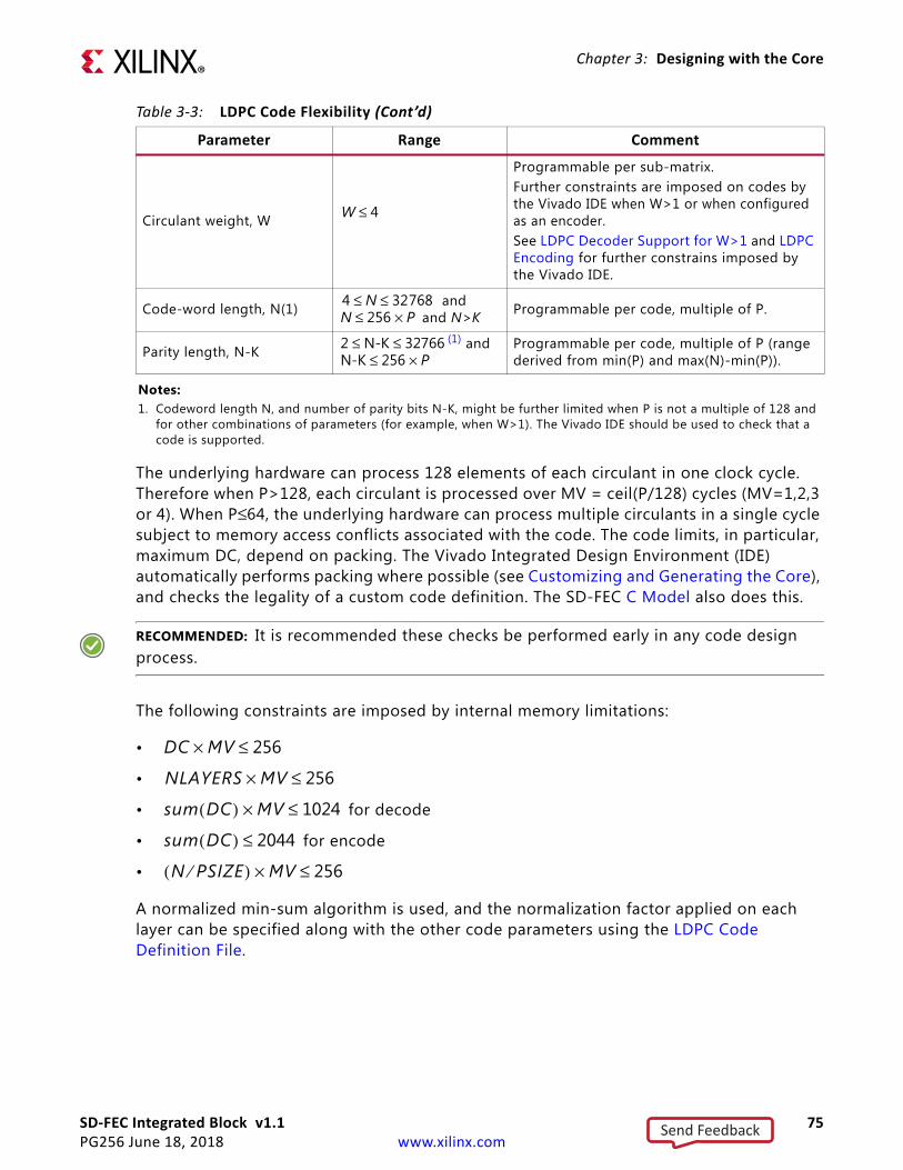
SD-FEC Integrated Block v1.1 75PG256 June 18, 2018 www.xilinx.com
Chapter 3: Designing with the Core
The underlying hardware can process 128 elements of each circulant in one clock cycle. Therefore when P>128, each circulant is processed over MV = ceil(P/128) cycles (MV=1,2,3 or 4). When P≤64, the underlying hardware can process multiple circulants in a single cycle subject to memory access conflicts associated with the code. The code limits, in particular, maximum DC, depend on packing. The Vivado Integrated Design Environment (IDE) automatically performs packing where possible (see Customizing and Generating the Core), and checks the legality of a custom code definition. The SD-FEC C Model also does this.
RECOMMENDED: It is recommended these checks be performed early in any code design process.
The following constraints are imposed by internal memory limitations:
•
•
• for decode
• for encode
•
A normalized min-sum algorithm is used, and the normalization factor applied on each layer can be specified along with the other code parameters using the LDPC Code Definition File.
Circulant weight, W
Programmable per sub-matrix.Further constraints are imposed on codes by the Vivado IDE when W>1 or when configured as an encoder.See LDPC Decoder Support for W>1 and LDPC Encoding for further constrains imposed by the Vivado IDE.
Code-word length, N(1) and and N>K Programmable per code, multiple of P.
Parity length, N-K(1) and Programmable per code, multiple of P (range
derived from min(P) and max(N)-min(P)).
Notes: 1. Codeword length N, and number of parity bits N-K, might be further limited when P is not a multiple of 128 and
for other combinations of parameters (for example, when W>1). The Vivado IDE should be used to check that a code is supported.
Table 3-3: LDPC Code Flexibility (Cont’d)
Parameter Range Comment
W 4≤
4 N 32768≤ ≤N 256 P×≤
2 N-K 32766≤ ≤N-K 256 P×≤
DC MV× 256≤
NLAYERS MV× 256≤
sum DC( ) MV× 1024≤
sum DC( ) 2044≤
N PSIZE⁄( ) MV× 256≤
Send Feedback

SD-FEC Integrated Block v1.1 76PG256 June 18, 2018 www.xilinx.com
Chapter 3: Designing with the Core
LDPC Decoding
LDPC Decoder Support for W>1
Decoder support for W>1 is only available for codes with P ≤ 128. When any code has W>1, then all codes that can be scheduled with it are limited to DC/PF×MV ≤ 64, irrespective of whether or not they employ W>1.
PF is the packing factor employed when PSIZE<128 (in which case MV is always 1). PF is the number of sub-matrices executed per cycle and can take values 1, 2 or 4 depending on PSIZE. So providing it is not disabled by NO_PACKING, the limit on DC becomes:
PSIZE ≤ 32 allows PF=4 and DC ≤ 256
PSIZE ≤ 64 allows PF=2 and DC ≤ 128
PSIZE ≤ 128 allows PF=1 and DCxMV ≤ 64
Note: When packing is employed, DC must accommodate any padding that is required.
The memory footprint of the code is increased by the number of circulants when W>1. This reduces the block size N that can be supported. For example, if PSIZE=128, and a code has two circulants in three sub-matrices, the effective block size becomes N+3*128.
Both the Vivado IDE and the C Model generate the necessary sequence of operations for a particular code, and ensure that these constraints are met. This check should be performed early in the design process to ensure that a code is supported.
Normalization
The LDPC Decoder implements a normalized min-sum algorithm whereby the contributions of each layer to the soft output are normalized by a scale factor. In 5G mode, the normalization factor can be specified per block on sc_idx field of CTRL. In non-5G NR mode the scale factor can be specified for each layer of a code using the SC_TABLE Register (Table 2-53). A default scaling factor of 0.75 is set by the Vivado IDE; however the optimum scaling factor depends on the LDPC code, and this should be established within the context of the system. This is particularly important for low-rate codes with high variable-node degrees.
It is assumed that the LLR input has been symmetrically saturated to 6 bits as summarized in Table 2-14. If this is not done, there can be significant performance degradation.
In Table 2-14, it is also suggested that the LLR is scaled to two fractional bits. However, LLR scaling is critical to performance and should be tuned within the context of the system to achieve optimal performance.
Send Feedback

SD-FEC Integrated Block v1.1 77PG256 June 18, 2018 www.xilinx.com
Chapter 3: Designing with the Core
Output Parity Check (OPC)
The decoder implements an on-line parity check to allow early termination (if enabled). There is also an option in the Vivado IDE, Include Output Parity Check, to implement a final parity check block, separately to the decoder. When enabled in the Vivado IDE, this determines whether the output produced on the final iteration passes the parity check when early termination does not occur or is not enabled (otherwise the value is that calculated by the on-line circuit for the previous iteration). Where possible, the check is performed in parallel with data output over DOUT, otherwise it is only the status output that is delayed until the updated pass flag is available. This takes a similar amount of time to one iteration of the decoder.
The OPC only supports codes where the total number of base matrix entries including any padding for packing (sum(packed(DC))) is less than or equal to 1024; OPC is automatically disabled by the core if an unsupported code is specified. This condition is also reported by the Vivado IDE. For large blocks it can also reduce peak throughput (although this is somewhat mitigated when smaller blocks are mixed with large blocks). Also, for codes with a large number of circulants per iteration, the maximum number of blocks interleaved can be reduced, increasing stall cycles and reducing throughput. The number of effective circulants can be increased by packing. To avoid throughput reduction, the final parity check can be turned off by setting NO_FINAL_PARITY_CHECK to 1. If information bit correctness is established using CRC, then the final parity has limited value, and the final parity check is not required. Note that early termination using a passing parity check can still be performed when the final parity check is disabled. Note that for the 5G NR standard the OPC is disabled because information bit correctness is established by a CRC check on the output of the decoder (parity pass can still be used for early termination).
LDPC EncodingThe LDPC encode is performed using a parity check matrix. The encoder supports matrices with lower triangular parity portion where the diagonal has a circulant weight of 1. It also supports a set of constrained matrices which have a double diagonal as employed by WiFi codes (WiFi 802.11ac-2012 High Throughput PHY [Ref 13]), and matrices that are a mix of double diagonal parity followed by a single diagonal as adopted by 5G wireless (3GPP TS 38.212 V.15.0.0 Multiplexing and channel coding (Release 15) [Ref 11]).
Examples of supported matrices are shown in Figure 3-2 to Figure 3-4. The base matrix elements in dark gray contain single circulants and have zero rotation. The patterned region of the matrix can contain multiple circulants in each sub-matrix and arbitrary rotation values.
Send Feedback

SD-FEC Integrated Block v1.1 78PG256 June 18, 2018 www.xilinx.com
Chapter 3: Designing with the Core
A lower triangular matrix, as shown in Figure 3-2, has a first layer containing a single circulant in the first parity column, with each new layer adding only one new circulant to the parity part of the matrix in the adjacent column. Additional circulants can be included in both the information and parity parts of the layer, but must be to the left of the new parity
X-Ref Target - Figure 3-2
Figure 3-2: Parity Check Matrix with Single DiagonalX-Ref Target - Figure 3-3
Figure 3-3: Parity Check Matrix with Double DiagonalX-Ref Target - Figure 3-4
Figure 3-4: Parity Check Matrix for 5G Wireless Graph 1
X19562-092117
X19563-092117
1 0
00
0
0
0
0
0
1
X19564-092717
Send Feedback

SD-FEC Integrated Block v1.1 79PG256 June 18, 2018 www.xilinx.com
Chapter 3: Designing with the Core
circulant. For such a matrix, it is possible to calculate parity by processing the layers from first layer to last, solving the parity check equation for the single unknown parity column.
When the matrix is double diagonal, as shown in Figure 3-3, the first layer contains two parity circulants in the first two parity columns, and the following layers contain another two parity circulants offset to the right by 1.
For such a matrix, there are two unknown parity columns in the first layer, and a direct solution is not possible. However, in many cases it is possible to transform the double diagonal matrix into a single diagonal matrix by adding rows to eliminate additional parity columns. For example, adding the last row of Figure 3-3 to the second last row results in the cancellation of the unwanted right-most circulant in the second-last row. Then, this resulting second-last row can be added to the third-last row, to cancel the unwanted right-most circulant, and likewise this process repeated up the rows, to finally obtain the matrix of Figure 3-2. This matrix is then suitable for encode. The main drawback of this method is that it can lead to additional operations in the information portion and under the triangular part of the parity portion, when row combinations have different rotations and so do not cancel.
Whilst the above method is more generally applicable, for a range of double diagonal matrices it is possible to implement a matrix with fewer operations. This exploits the property of the matrix that the sum of all the layers in the parity check matrix gives a check equation containing only the first parity column. That is when all the circulants in each column of the parity part of the check matrix are summed, then that sum is 0 for all but the first row where it is a single circulant. This new check equation can be used to solve for the first parity bit, and the existing check equations (layers of the parity check matrix) providing solutions for the remaining parity bits.
For example, Figure 3-4 shows a portion of the 5G wireless graph 1 parity check matrix. Only the parity portion is shown in detail. In particular, the circulant rotation is shown as a number in the sub-matrix. The first four layers can be summed to provide an equation for the first parity bit. That is, the sum of the parity column consists of the modulo 2 addition of three circulants with rotation 1,0 and 1. The two circulants with rotation 1 cancel leaving a circulant with rotation 0. The other columns contain two circulants with rotation 0 and, likewise, they cancel, leaving only the circulant in first parity column.
Figure 3-4 also shows a mix of double diagonal and diagonal matrices. When the first parity column has been derived, the remaining parity can be calculated as each new layer is only adding one new column of parity.
Double diagonal matrices, with the property described, are supported directly by the Vivado IDE. Note that a further optimization is applied in the solution implemented that reuses layer products, and as a consequence the additional operations over-and-above that of the parity check matrix are relatively small.
Send Feedback

SD-FEC Integrated Block v1.1 80PG256 June 18, 2018 www.xilinx.com
Chapter 3: Designing with the Core
LDPC Peak ThroughputNote: The encoder calculation is the same as the decoder calculation with Niter set to 1.
Throughput is code-specific and depends on a number of factors including data dependences in the code. However, peak throughput of the LDPC decoder (measured for information bits at the output) for P = 128, is given by:
Equation 3-1
• fcore_clk is the core clock frequency.
• Niter is the number of iterations performed.
• avg(DV) is the average variable node degree of the code (total number of circulants in the parity check matrix divided by the number of columns—in effect, the number of circulants per bit of the codeword).
The factor of 128 in the given equation is associated with the level of parallelism implemented in the SD-FEC core (128 check-node and variable node processors are implemented).
The given throughput equation assumes no data dependencies arising from the code, and that P is a multiple of 128. If P is not a multiple of 128, then there is under-utilization of the decoder processing resources, and throughput degrades by a factor of P/(128×MV) where
.
For example, if P = 360, then
Equation 3-2
Therefore actual throughput = Peak throughput × 360/384.
Input, decoding and output are pipelined, and for small blocks there is sufficient memory to hold multiple blocks. When there is sufficient memory available, the core interleaves multiple blocks during encode/decode to hide data dependencies.
For codes where W>1, operations are added for each circulant in a sub-matrix where W>1, and consequently throughput is reduced. (For example, for one codeword with two sub-matrices containing two circulants each, four additional operations are required). There are also further data dependencies which might require greater codeword interleaving to hide (where memory allows).
Throughput might also be limited for large block sizes, as the opportunity to overlap decoding with I/O is reduced by memory limitations.
Peak Throughput 128avg DV( )Niter----------------------------- Rate× fcore_clk×=
MV P128--------=
360128 MV×-------------------- 360
128 3×---------------- 360
384--------= =
Send Feedback

SD-FEC Integrated Block v1.1 81PG256 June 18, 2018 www.xilinx.com
Chapter 3: Designing with the Core
Reuse of LDPC Code Base MatricesIt is possible to reuse a single base matrix to support different code rates and/or codeword sizes in the following ways:
1. Change the sub-matrix size to support different codeword sizes at the same rate. For each code specify a different PSIZE, N and K (as defined in REG0-2), whilst keeping the offset parameters in the shared code definition tables (that is, SC_OFF, LA_OFF and QC_OFF in REG3) the same.
2. Reuse only a portion of the base matrix to support different codeword sizes and rates, but with the same K. If the base matrix takes the form shown in Figure 3-5 (more specifically, the column of the right-most non-zero sub-matrix increases monotonically with layer), then it is possible to reduce the number of columns in the base matrix by reducing the number of layers, NLAYERS, and N in the code definition while keeping the offset parameters in the shared code definition tables (that is, SC_OFF, LA_OFF and QC_OFF) the same. The rate increases as the number of parity bits and codeword size is reduced.
For method 1 if PSIZE ≤ 64 then packing is performed (unless NO_PACKING field is set in the code definition register). In this case, the QC_TABLE entries are different. As such, for support of all PSIZE, at least three sets of QC_TABLEs are required (that is, one for PSIZE ≤ 32, one for 32 < PSIZE ≤ 64 and one for PSIZE > 64. Furthermore, a method to reduce the rotation to be less than PSIZE is required, although this might be done from the largest value using a suitable reduction operation, for example, modulo(ROTATION, PSIZE).
If this operation results in differences between the rotation values for the two codes, then a separate set of entries is required in the QC_TABLE. For example, if the PSIZE for two codes was 33 and 64, and the rotation value was 48, then, because 48 is greater than 33, there would need to be a reduced value specified for PSIZE = 33 and, as a consequence, the QC_TABLE entries for each code would need to be defined separately. If all the rotation
X-Ref Target - Figure 3-5
Figure 3-5: Changing Number of Columns in Base Matrix by Adjusting NLAYERS
K
N
Rate increases as number of layers
(NLAYERS) is reduced. K stays the same, N
reduces.
Send Feedback
SD-FEC Integrated Block v1.1 82PG256 June 18, 2018 www.xilinx.com
Chapter 3: Designing with the Core
values were less than 33, then only one set of entries would need to be defined in the QC_TABLE for both codes.
For method 2, the stall parameters (in LA_TABLE) might change with the number of layers. Analysis of the changes can be performed by passing the code with different numbers of layers through the core API (see LDPC Runtime Configuration) to generate the instruction tables. The amount of variation depends upon the code, but it is likely that the number of variants can be significantly reduced to less than one LA_TABLE per codeword size. It might also be possible to further reduce the number of tables by setting the stall values to be the maximum of those generated by the API. That is, it is safe to use a STALL value larger than that provided by the API, although this might have implications on throughput.
With either method, it is necessary to provide code parameters (that is, REG0-3) for each code variant. There are 128 register sets available to support this. The shared code parameters SC_TABLE, LA_TABLE, QC_TABLE can be apportioned as necessary between unique codes, and combined in an arbitrary fashion by the code parameters for a particular code definition. If these are to be re-written, then it might be appropriate to sub-divide the tables into a number of equal size partitions to allow each partition to be written independently.
Methods 1 and 2 can be combined to obtain greater flexibility.
LDPC Code Memory Error Detection and CorrectionLDPC code parameters, REF, and shared tables are stored in memories with Error Correction Code (ECC). This memory has the ability to detect two errors, and correct one error. For each memory, two error flags are generated and made available through the interrupt service register in order to monitor errors:
• ECC error: normally 0, set when one or more errors have been detected in a word read from the respective memory.
• ECC two-bit error: normally 0, set when 2 errors are detected in a word read from the respective memory. It may also be set when the number of errors in a word is greater than 2, however, this is not guaranteed.
Send Feedback

SD-FEC Integrated Block v1.1 83PG256 June 18, 2018 www.xilinx.com
Chapter 4
Design Flow StepsThis chapter describes customizing and generating the core, constraining the core, and the simulation, synthesis and implementation steps that are specific to this IP core. More detailed information about the standard Vivado® design flows and the IP integrator can be found in the following Vivado Design Suite user guides:
• Vivado Design Suite User Guide: Designing IP Subsystems using IP Integrator (UG994) [Ref 3]
• Vivado Design Suite User Guide: Designing with IP (UG896) [Ref 4]
• Vivado Design Suite User Guide: Getting Started (UG910) [Ref 5]
• Vivado Design Suite User Guide: Logic Simulation (UG900) [Ref 6]
Customizing and Generating the CoreThis section includes information about using Xilinx® tools to customize and generate the core in the Vivado Design Suite.
If you are customizing and generating the core in the Vivado IP Integrator, see the Vivado Design Suite User Guide: Designing IP Subsystems using IP Integrator (UG994) [Ref 3] for detailed information. IP integrator might auto-compute certain configuration values when validating or generating the design. To check whether the values do change, see the description of the parameters in this chapter. To view the parameter values, run the validate_bd_design command in the Tcl console.
You can customize the IP core for use in your design by specifying values for the various parameters associated with the IP core using the following steps:
1. Select the IP from the Vivado IP catalog.
2. Double-click the selected IP or select the Customize IP command from the toolbar or right-click menu.
For details, see the Vivado Design Suite User Guide: Designing with IP (UG896) [Ref 4] and the Vivado Design Suite User Guide: Getting Started (UG910) [Ref 5].
Send Feedback

SD-FEC Integrated Block v1.1 84PG256 June 18, 2018 www.xilinx.com
Chapter 4: Design Flow Steps
The SD-FEC core configuration screen in the Vivado IDE comprises four configuration tabs and four information tabs.
IP Symbol TabThe IP Symbol tab shows the core pinout.
Interface Summary TabThis tab displays the field types, widths and positions of the core AXI4-Stream interfaces.
LDPC Code Analysis TabThis tab displays any messages generated while processing the specified LDPC codes, for example, decoder/encoder compatibility and warnings of any default values being used.
LDPC Table Usage TabWhen the core is configured for LDPC Decode or Encode, this tab reports the total utilization of the Shared LDPC Code Parameters for the specified LDPC codes. In addition, it reports the relative utilization for each code.
Function TabThis tab is used to specify the FEC mode and configuration.
Note: A single IP instance can only be configured for Turbo decode or LDPC operation. When configured for LDPC Encode, the control stream operation bit is fixed to Encode (see Control AXI4-Stream Slave).
Configuration
Standard: Specifies which of the supported standards the block is to be used: LTE, 5G New Radio [Ref 11], WIFI 802.11 [Ref 13], DOCSIS 3.1 [Ref 12] or a custom LDPC code definition.
Turbo Decode Code Parameters
• Turbo Decode: Selects Turbo Decode FEC mode.
• Algorithm: Specifies which Turbo Decode algorithm to use:
° MAX Scale: Max Log-Map algorithm with extrinsic scaling. When scaling is set to 1 this is equivalent to the Max Log-Map algorithm.
° MAX Star: Log-Map algorithm.
• Scale: Specifies the extrinsic scaling to apply when the Max Scale algorithm has been selected. The scale is defined as 0.0625-1, in increments of 0.0625. The default value is 0.75.
Send Feedback

SD-FEC Integrated Block v1.1 85PG256 June 18, 2018 www.xilinx.com
Chapter 4: Design Flow Steps
LDPC Decode Code Parameters
• LDPC Decode: Selects LDPC Decode FEC mode.
• Support W>1: Specifies whether codes with W>1 are supported. This results in additional checks on all codes being run on the decoder. See LDPC Decoder Support for W>1 for more details.
• Code Definition: LDPC code definition file. This is a YAML file (http://yaml.org) which specifies the custom LDPC code definitions for use with the IP instance. See LDPC Code Definition File for details of file format.
IMPORTANT: The code definition file must have a .txt extension.
• Enable Overrides: Enables the following parameter overrides:
Overrides are not available when the 5G standard has been selected.
Values set in the Vivado IDE override those defined in the specified YAML file or standard.
° No Final Parity Check: Disables the output parity check logic. Increases throughput for large codes. See Output Parity Check (OPC) for further details.
° Scale: Layer scaling factor. The core uses a default of 0.75 if undefined in the YAML file. The scale is defined as 0.0625-1, in increments of 0.0625. The default value is 0.75.
° Max. Schedule: Sets the maximum code block interleaving. See REG2 Register (0x2008+CODE*0x10)(1).
LDPC Encode Code Parameters
Note: Some LDPC codes suitable for Decode are not suitable for Encode - errors are reported, detailing any incompatibilities. See LDPC Encoding for more details.
• LDPC Encode: Selects LDPC Encode FEC mode. This selection is compatible with LDPC Decode.
• Code Definition: LDPC code definition file. This is a YAML file (http://yaml.org) which specifies the custom LDPC code definitions for use with the IP instance. See LDPC Code Definition File for details of file format.
IMPORTANT: The code definition file must have a .txt extension.
Send Feedback
SD-FEC Integrated Block v1.1 86PG256 June 18, 2018 www.xilinx.com
Chapter 4: Design Flow Steps
Interface TabThis tab is used to configure the interface settings.
S_AXI
• Interface: Specifies the S_AXI parameter interface configuration.
° Runtime-Configured: the S_AXI interface is exposed and the core and LDPC parameters must be configured by an external source. The IP core generates configuration parameters which are written to a file (see LDPC Runtime Configuration for more details) and also exported to the standalone driver in SDK.
° Initialized retain I/F: The code parameters are automatically initialized at device configuration or post reset. Initialization values for the core parameter can also be specified using the corresponding core configuration screen parameters.
° Initialized: The S_AXI interface is removed from IP and the Enable I/Fs core parameter is set.
• Core Parameters: Specifies initialization values for the following core parameters when the Interface configuration is set to Initialized retain I/F or Initialized.
° Enable I/Fs: Set all interfaces enable bits in the AXIS_ENABLE register.
° Out of Order: Sets the out of order bit in the ORDER register.
° Interrupts: Clears all bits of the Interrupt Mask register, thereby enabling interrupts.
° ECC Interrupts: None, Both or Multi-bit Only.
- Both: All bits of the ECC Interrupt Mask register are cleared, enabling all ECC interrupts.
- Multi-bit Only: Only the two-bit ECC error bits are cleared, enabling only the two-bit ECC interrupts.
° Bypass: Sets the BYPASS register.
° AXI WR Protect: Sets the AXI_WR_PROTECT register.
° Code WR Protect: Sets the CORE_WR_PROTECT register.
See Register Space for more details.
DIN
See Data Interfaces for full details of the interface configuration options. These options configure the AXIS_WIDTH register (see Table 2-35).
• Interface: Specifies the DIN and DIN_WORDS interface configuration. When Unconfigured, the full interfaces are exposed as detailed in Port Descriptions. When Pre-configured, the interface is simplified as per the Vivado IDE settings.
• Lanes: Specifies the number of DIN lanes exposed on the IP instance (1, 2 or 4).
Send Feedback
SD-FEC Integrated Block v1.1 87PG256 June 18, 2018 www.xilinx.com
Chapter 4: Design Flow Steps
• Words configuration: Specifies the DIN_WORDS configuration: Fixed, Per Block or Per Transaction.
When Fixed, the DIN_WORDS AXI4-Stream interface is removed from the IP instance and is driven with the specified number of words.
When Per Block or Per Transaction is selected, the DIN_WORDS interface is present:
° Per Block configures the IP instance to expect a single DIN_WORDS value per input code block.
° Per Transaction configures the IP instance to expect one DIN_WORDS value per input transaction on the DIN interface.
• Number of words: Specifies the fixed number of words that is expected on the DIN interface for every transaction. This is used when the words configuration is set to Fixed.
DOUT
• Interface: Specifies the DOUT and DOUT_WORDS interface configuration. When Unconfigured, the full interfaces are exposed as detailed in Port Descriptions. When Pre-configured, the interface is simplified as per the Vivado IDE settings.
• Lanes: Specifies the number of DOUT lanes exposed on the IP instance (1, 2 or 4).
• Words configuration: Specifies if the DOUT_WORDS configuration: Fixed, Per Block or Per Transaction.
When Fixed, the DOUT_WORDS AXI4-Stream interface is removed from the IP instance and is driven with the specified number of words. The DOUT AXI4-Stream interface transmits with the specified number of words.
When Per Block or Per Transaction is selected, the DOUT_WORDS AXI4-Stream interface is present:
° Per Block configures the IP instance to expect a single DOUT_WORDS value per output code block.
° Per Transaction configures the IP instance to expect one DOUT_WORDS value per output transaction on the DOUT AXI4-Stream interface.
• Number of words: Specifies the fixed number of words that is expected on the DOUT interface for every transaction. This is used when the words configuration is set to Fixed.
Runtime Loading TabThis tab is used to set the runtime activity. The physical and throughput utilization values are used to determine the power estimate for the IP instance by defining the expected runtime activity. The physical utilization value is automatically calculated using the characteristics of the specified code(s).
Send Feedback
SD-FEC Integrated Block v1.1 88PG256 June 18, 2018 www.xilinx.com
Chapter 4: Design Flow Steps
• Physical Utilization: Defines the utilization of SD-FEC functional blocks. The parameter value is calculated automatically based on the specified code configuration.
• Throughput Utilization: Specifies activity in terms of instance throughput as a percentage of maximum throughput for the code configurations in use. For example, the maximum throughput of the DOCSIS v3.1 medium code is 1.57 Gb/s but if the block is operated at 1 Gb/s the activity figure can be reduced to ~64%. Note, the maximum throughput when different codes are interleaved can be higher or lower than the throughput of the individual codes.
IMPORTANT: The following runtime loading parameters have been deprecated and are no longer available unless you are upgrading from a previous revision of the IP core where these parameters had been set to non-default values.
• Percentage Loading: Automatic or Manual. When Automatic, the appropriate Percentage Loading parameter is updated based on the Throughput Utilization parameter and the specific Turbo or LDPC code parameters. When Manual is selected, the following percentage loading parameters can be modified:
° Turbo Decoder Percentage Loading: Percentage of maximum activity loading for this IP instance when configured for Turbo Decode.
° LDPC Decoder Percentage Loading: Percentage of maximum activity loading for this IP instance when configured for LDPC Decode.
° LDPC Encode Percentage Loading: Percentage of maximum activity loading for this IP instance when configured for LDPC Encode only.
Example Design TabThis tab is used to set the example design parameters.
The core always generates the default simulation-only example test bench example design. A processor-based example design can also be selected; this is included in the example design along with the default example test bench.
• Generate processor-based example design: Select the generation of the processor based example design in the example design project.
• Processor-based example design type: Select MicroBlaze or Zynq UltraScale+ RFSoC.
° Selecting MicroBlaze, enables simulation of the full processor-based example design.
° Selecting ZYNQ UltraScale+ RFSoC, creates an example design using the Processor Sub-System (PS).
Example design generation also builds an example processor application.
Send Feedback

SD-FEC Integrated Block v1.1 89PG256 June 18, 2018 www.xilinx.com
Chapter 4: Design Flow Steps
• Include Encoder instance: When selected the generated example design also includes an instance of the LDPC Encoder/Decoder IP core configured for encode. This option is only available when LDPC Encode or Decode has been selected and the core is able to determine a LDPC code definition compatible with the LDPC encoder.
• Build SDK Project: Optionally attempt to create and build the example processor application during example design generation. This step requires the Xilinx Software Command line Tool (XSCT) to be available. The generated ELF is imported into the example design and associated with the MicroBlaze processor, enabling simulation of the example design.
User ParametersTable 4-1 shows the relationship between the fields in the Vivado IDE and the User Parameters (which can be viewed in the Tcl Console).
Table 4-1: Vivado IDE Parameter to User Parameter Relationship
Vivado IDE Parameter/Value(1) User Parameter/Value(1) Default Value
Function: Configuration
Standard Standard LTE
Function: Turbo Decode Code parameters
Algorithm Turbo_Decode_Algorithm MaxScale
Scale Turbo_Decode_Scale
[1.0, 0.0625:0.0625:0.9375] [0, 1:1:15] 12
Function: LDPC Decode Code Parameters
LDPC Decode LDPC_Decode False
Support W>1 Enable_Wgt1 False
Code Definition LDPC_Decode_Code_Definition no_file_loaded
Enable LDPC_Decode_Overrides False
No Final Parity Check LDPC_Decode_No_OPC False
Scale LDPC_Decode_Scale
[1.0, 0.0625:0.0625:0.9375] [0, 1:1:15] 12
Max. Schedule LDPC_Decode_Max_Schedule 0
Function: LDPC Encode Code Parameters
LDPC Encode LDPC_Encode False
Code Definition LDPC_Encode_Code_Definition no_file_loaded
Interface: S_AXI
Interface Parameter_Interface Runtime-Configured
Enable I/Fs Enable_IFs False
Out of Order Out_of_Order False
Send Feedback
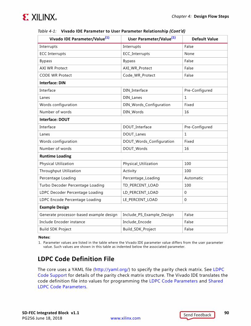
SD-FEC Integrated Block v1.1 90PG256 June 18, 2018 www.xilinx.com
Chapter 4: Design Flow Steps
LDPC Code Definition FileThe core uses a YAML file (http://yaml.org/) to specify the parity check matrix. See LDPC Code Support for details of the parity check matrix structure. The Vivado IDE translates the code definition file into values for programming the LDPC Code Parameters and Shared LDPC Code Parameters.
Interrupts Interrupts False
ECC Interrupts ECC_Interrupts None
Bypass Bypass False
AXI WR Protect AXI_WR_Protect False
CODE WR Protect Code_WR_Protect False
Interface: DIN
Interface DIN_Interface Pre-Configured
Lanes DIN_Lanes 1
Words configuration DIN_Words_Configuration Fixed
Number of words DIN_Words 16
Interface: DOUT
Interface DOUT_Interface Pre-Configured
Lanes DOUT_Lanes 1
Words configuration DOUT_Words_Configuration Fixed
Number of words DOUT_Words 16
Runtime Loading
Physical Utilization Physical_Utilization 100
Throughput Utilization Activity 100
Percentage Loading Percentage_Loading Automatic
Turbo Decoder Percentage Loading TD_PERCENT_LOAD 100
LDPC Decoder Percentage Loading LD_PERCENT_LOAD 0
LDPC Encode Percentage Loading LE_PERCENT_LOAD 0
Example Design
Generate processor-based example design Include_PS_Example_Design False
Include Encoder instance Include_Encode False
Build SDK Project Build_SDK_Project False
Notes: 1. Parameter values are listed in the table where the Vivado IDE parameter value differs from the user parameter
value. Such values are shown in this table as indented below the associated parameter.
Table 4-1: Vivado IDE Parameter to User Parameter Relationship (Cont’d)
Vivado IDE Parameter/Value(1) User Parameter/Value(1) Default Value
Send Feedback
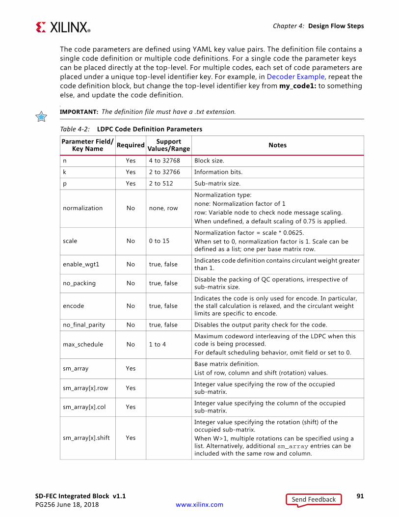
SD-FEC Integrated Block v1.1 91PG256 June 18, 2018 www.xilinx.com
Chapter 4: Design Flow Steps
The code parameters are defined using YAML key value pairs. The definition file contains a single code definition or multiple code definitions. For a single code the parameter keys can be placed directly at the top-level. For multiple codes, each set of code parameters are placed under a unique top-level identifier key. For example, in Decoder Example, repeat the code definition block, but change the top-level identifier key from my_code1: to something else, and update the code definition.
IMPORTANT: The definition file must have a .txt extension.
Table 4-2: LDPC Code Definition Parameters
Parameter Field/Key Name Required Support
Values/Range Notes
n Yes 4 to 32768 Block size.
k Yes 2 to 32766 Information bits.
p Yes 2 to 512 Sub-matrix size.
normalization No none, row
Normalization type:none: Normalization factor of 1row: Variable node to check node message scaling.When undefined, a default scaling of 0.75 is applied.
scale No 0 to 15Normalization factor = scale * 0.0625. When set to 0, normalization factor is 1. Scale can be defined as a list; one per base matrix row.
enable_wgt1 No true, false Indicates code definition contains circulant weight greater than 1.
no_packing No true, false Disable the packing of QC operations, irrespective of sub-matrix size.
encode No true, falseIndicates the code is only used for encode. In particular, the stall calculation is relaxed, and the circulant weight limits are specific to encode.
no_final_parity No true, false Disables the output parity check for the code.
max_schedule No 1 to 4Maximum codeword interleaving of the LDPC when this code is being processed.For default scheduling behavior, omit field or set to 0.
sm_array YesBase matrix definition.List of row, column and shift (rotation) values.
sm_array[x].row Yes Integer value specifying the row of the occupied sub-matrix.
sm_array[x].col Yes Integer value specifying the column of the occupied sub-matrix.
sm_array[x].shift Yes
Integer value specifying the rotation (shift) of the occupied sub-matrix.When W>1, multiple rotations can be specified using a list. Alternatively, additional sm_array entries can be included with the same row and column.
Send Feedback

SD-FEC Integrated Block v1.1 92PG256 June 18, 2018 www.xilinx.com
Chapter 4: Design Flow Steps
Decoder Example
my_code1:n: 128k: 104p: 8scale: [11,11,11]sm_array:- {row: 0, col: 0, shift: [1,6]} # defines multiple rotations (for W>1 codes)- {row: 0, col: 2, shift: 5}- {row: 0, col: 6, shift: 4}- {row: 0, col: 7, shift: 3}- {row: 0, col: 11, shift: 2}- {row: 0, col: 12, shift: 1}- {row: 0, col: 14, shift: 0}- {row: 0, col: 15, shift: 7}- {row: 1, col: 0, shift: 6}- {row: 1, col: 1, shift: 7}- {row: 1, col: 5, shift: 0}- {row: 1, col: 7, shift: 1}- {row: 1, col: 9, shift: 2}- {row: 1, col: 11, shift: 3}- {row: 1, col: 15, shift: 4}- {row: 2, col: 0, shift: 0}- {row: 2, col: 3, shift: 1}- {row: 2, col: 4, shift: 2}- {row: 2, col: 8, shift: 3}- {row: 2, col: 9, shift: 4}- {row: 2, col: 10, shift: 5}- {row: 2, col: 13, shift: 6}
Encoder Example
my_enc_code1: encode: true k: 280 n: 448 p: 56 sm_array:
- {row: 0, col: 0, shift: [1,6]} # defines multiple rotations (for W>1 codes)- {row: 0, col: 2, shift: 34}
- {row: 0, col: 3, shift: 7} - {row: 0, col: 4, shift: 46} - {row: 0, col: 5, shift: 10} - {row: 1, col: 0, shift: 2} - {row: 1, col: 1, shift: 23} - {row: 1, col: 2, shift: 0} - {row: 1, col: 3, shift: 51} - {row: 1, col: 5, shift: 49} - {row: 1, col: 6, shift: 20} - {row: 2, col: 0, shift: 19} - {row: 2, col: 1, shift: 18} - {row: 2, col: 2, shift: 52} - {row: 2, col: 4, shift: 37} - {row: 2, col: 6, shift: 34} - {row: 2, col: 7, shift: 39}
Send Feedback

SD-FEC Integrated Block v1.1 93PG256 June 18, 2018 www.xilinx.com
Chapter 4: Design Flow Steps
Output GenerationFor details, see the Vivado Design Suite User Guide: Designing with IP (UG896) [Ref 4].
LDPC Runtime Configuration
The Vivado IDE provides two methods to generate the code configuration parameters, either during IP core generation or through a TCL interface. The latter is particularly useful when it is necessary to generate a wide range of codes, because it allows the parameter configuration to be analyzed, thereby establishing commonalities and minimizing the amount of parameter storage required. It can also be used to verify that any custom parameter generation method is generating the correct parameters for a particular code requirement.
IP Core Generation
The AXI4-Lite transactions required to configure the SD-FEC core at run-time are produced during IP generation. The options set in the Vivado IDE are imported by the standalone software driver and are also written to a command file for use with a programmable logic based controller; <ipinst>_trans.log. The IP Sources window displays all the generated output products for an IP core. The default output product directory for an IP core is in the project directory, <project_name>.srcs/sources_1/ip/<ipinst_name>. The command file is text and contains a list of address and data pairs in hexadecimal.
TCL Interface
An additional TCL script, <project_name>.srcs/sources_1/ip/<ipinst_name>/scripts/gen_ldpc_code_params.tcl is output during IP core generation which contains a helper function, gen_ldpc_code_params, which can be used to process the LDPC Code Definition File independent of the Vivado IDE. To make the function available in the Vivado TCL shell, enter the following command:
source <project_name>.srcs/sources_1/ip/<ipinst_name>/scripts/gen_ldpc_code_params.tcl
The function requires a single argument of a code definition file and returns a TCL dict structure containing the configuration parameters for the LDPC Code Parameters and Shared LDPC Code Parameters for each of the LDPC codes defined in the file.
The TCL dict consists of a top-level key per code defined in the code definition file below which all the corresponding parameters are defined. The dict structure can be queried to obtain the configuration parameters for each code, for example:
set params [gen_ldpc_code_params <my_code_definition_file>]set all_code_ids [dict keys $params]set all_param_names [dict keys [dict get $params <my_code_id1>]]set n [dict get $params <my_code_id1> n]set k [dict get $params <my_code_id1> k]set qc_table [dict get $params <my_code_id1> qc_table]
Send Feedback
SD-FEC Integrated Block v1.1 94PG256 June 18, 2018 www.xilinx.com
Chapter 4: Design Flow Steps
Constraining the CoreThis section contains information about constraining the core in the Vivado Design Suite.
Required ConstraintsThe Vivado IDE implementation currently does not support automatic timing-driven placement for SD-FEC instances. To achieve optimal timing results, the instances must be placed manually:
set_property LOC FE_X<x>Y<y> [get_cells */<ipinst_name>/inst/FE_I]
IMPORTANT: Combinations of SD-FEC instances are restricted according to LDPC or Turbo mode. See Placement Location Guidelines for SD-FEC IP Core for further guidelines and placement locations when using multiple instances of the SD-FEC.
Device, Package, and Speed Grade SelectionsThe core can be implemented in Zynq UltraScale+ RFSoC devices as detailed in the Zynq UltraScale+ RFSoC Data Sheet: Overview (DS889) [Ref 2].
Clock FrequenciesSee the Zynq UltraScale+ RFSoC Data Sheet: Overview (DS889) [Ref 2].
Clock ManagementThis section is not applicable for this IP core.
Clock PlacementThis section is not applicable for this IP core.
BankingThis section is not applicable for this IP core.
Transceiver PlacementThis section is not applicable for this IP core.
I/O Standard and PlacementThis section is not applicable for this IP core.
Send Feedback

SD-FEC Integrated Block v1.1 95PG256 June 18, 2018 www.xilinx.com
Chapter 4: Design Flow Steps
SimulationFor comprehensive information about Vivado simulation components, as well as information about using supported third-party tools, see the Vivado Design Suite User Guide: Logic Simulation (UG900) [Ref 6].
Synthesis and ImplementationFor details about synthesis and implementation, see the Vivado Design Suite User Guide: Designing with IP (UG896) [Ref 4].
Placement Location Guidelines for SD-FEC IP CoreAll SD-FEC instances must be placed using an XDC constraint. See Required Constraints for more information. Certain placement and use guidelines are dependent on the selected SD-FEC mode. Table 4-3 shows placement options for configurations of Turbo, LDPC encoder, and LDPC decoder instances; the LDPC encoder instances have no placement restrictions but the Turbo and LDPC decoder placement guidelines must be followed.
The following SD-FEC configurations are supported:
1. A maximum of four Turbo mode SD-FEC instances can be used simultaneously.
2. A maximum of eight SD-FEC instances can be used simultaneously, with up to six performing LDPC decode.
3. A mixed mode of Turbo decode and LDPC decode and encode is also supported up to a maximum of four SD-FEC instances. The placement guidelines for this configuration are the same as for Turbo mode in Table 4-3.
The Vivado design tools issue an error if the combinations in Table 4-3 are not followed. See the device diagram (Figure 4-1) for reference to the SD-FEC block locations.
Send Feedback

SD-FEC Integrated Block v1.1 96PG256 June 18, 2018 www.xilinx.com
Chapter 4: Design Flow Steps
Table 4-3: Placement Guidelines
Turbo Mode(1) LDPC Mode(1)FMAX (MHz)
Decoder(2) Encoder
-2 Speed Grades (Vnom Only)
X0Y7, X0Y5, X0Y3, X0Y1None None 667
X0Y7, X0Y6, X0Y1, X0Y0
None
X0Y7, X0Y6, X0Y5,X0Y2, X0Y1, X0Y0
X0Y4, X0Y3
667None
None X0Y7, X0Y6, X0Y5, X0Y4,X0Y3, X0Y2, X0Y1, X0Y0
-1 Speed Grades (Vnom Only)
X0Y7, X0Y5, X0Y3, X0Y1None None 667
X0Y7, X0Y6, X0Y1, X0Y0
None
X0Y7, X0Y6, X0Y5,X0Y2, X0Y1, X0Y0
X0Y4, X0Y3
625None
None X0Y7, X0Y6, X0Y5, X0Y4,X0Y3, X0Y2, X0Y1, X0Y0
All Speed Grades
X0Y7, X0Y5, X0Y3, X0Y1None None 667
X0Y7, X0Y6, X0Y1, X0Y0
None
X0Y7, X0Y6, X0Y1, X0Y0 X0Y5, X0Y2
667X0Y7, X0Y5, X0Y3 X0Y1 None
None X0Y7, X0Y6, X0Y5,X0Y2, X0Y1, X0Y0
Notes: 1. Subsets of these configurations are also allowed; for example, four LDPC decoders and four LDPC encoders is a
valid setting, provided that the LDPC decoders are always placed in the specified decoder sites. 2. LDPC encoders can be placed in any valid LDPC decoder site.
X-Ref Target - Figure 4-1
Figure 4-1: SD-FEC Locations in the SD-FEC Column
X0Y7X0Y6X0Y5X0Y4X0Y3X0Y2X0Y1X0Y0
X19907-100317
Send Feedback
SD-FEC Integrated Block v1.1 97PG256 June 18, 2018 www.xilinx.com
Chapter 5
C ModelThis chapter details the C Model provided with the core.
The bit accurate C model is a self-contained, linkable, shared library that models the functionality of the SD-FEC core with finite precision. The model consists of a set of C functions that reside in a shared library.
The model is bit accurate but not cycle-accurate; it does not model the core latency or its interface signals. Example C code is provided to demonstrate how these functions form the interface to the C model.
The C model has been tested on Linux using GCC 4.4.7 and 4.8.0, and on Windows using Visual Studio 2012 and MinGW GCC 4.9.0. MATLAB R2013a has been used.
Note: The shared object and DLL are statically linked with libstdc++, ensuring it has access to the correct version.
Unpacking and Model ContentsTable 5-1 and Table 5-2 show the zip file contents for both Linux and Windows C Models.
Table 5-1: Linux 64 Zip File Contents
File Description
Standard Header Files
sd_fec_v1_1_bitacc_cmodel.h Header file defining the C model API
xip_common_bitacc_cmodel.h Header file defining standard Xilinx® C model types and macros
Shared Objects
libIp_sd_fec_v1_1_bitacc_cmodel.so Model shared object library
MATLAB Wrapper
sd_fec_v1_1_bitacc_mex.cpp MATLAB® MEX function source
gen_ldpc_spec.mNon-class wrapper functions.
gen_parity_check_mat.m
@sd_fec_v1_1_bitacc MATLAB MEX function class directory
Send Feedback

SD-FEC Integrated Block v1.1 98PG256 June 18, 2018 www.xilinx.com
Chapter 5: C Model
Compilation and Smoke Tests
run_bitacc_cmodel.c Example program for calling the C model
make_run_bitacc_cmodel.csh Compilation script for example C program
make_sd_fec_v1_1_bitacc_mex.m MATLAB MEX function compilation script
run_sd_fec_v1_1_bitacc_mex.m MATLAB MEX function example script
Data Files
test.mat MATLAB MAT file containing example LDPC parity check matrix.
test.yml Example LDPC parity check matrix specification file, as required by model.
Table 5-2: Windows NT64 Zip File Contents
File Description
Standard Header Files
sd_fec_v1_1_bitacc_cmodel.h Header file defining the C model API
xip_common_bitacc_cmodel.h Header file defining standard Xilinx C model types and macros
DLL and Lib Objects
libIp_sd_fec_v1_1_bitacc_cmodel.dll Model DLL
libIp_sd_fec_v1_1_bitacc_cmodel.lib Model .lib file for compiling
MATLAB Wrapper
sd_fec_v1_1_bitacc_mex.cpp MATLAB® MEX function source
gen_ldpc_spec.mNon-class wrapper functions.
gen_parity_check_mat.m
@sd_fec_v1_1_bitacc MATLAB MEX function class directory
Compilation and Smoke Tests
run_bitacc_cmodel.c Example program for calling the C model
make_run_bitacc_cmodel.bat Compilation script for example C program
make_sd_fec_v1_1_bitacc_mex.m MATLAB MEX function compilation script
run_sd_fec_v1_1_bitacc_mex.m MATLAB MEX function example script
Data Files
test.mat MATLAB MAT file containing example LDPC parity check matrix.
test.yml Example LDPC parity check matrix specification file, as required by model.
Table 5-1: Linux 64 Zip File Contents (Cont’d)
File Description
Send Feedback

SD-FEC Integrated Block v1.1 99PG256 June 18, 2018 www.xilinx.com
Chapter 5: C Model
Installation
Linux• Unpack the contents of the zip file.
• Ensure that the directory where the libIp_sd_fec_v1_1_bitacc_cmodel.so file resides is included in the path of the environment variable LD_LIBRARY_PATH.
Windows• Unpack the contents of the zip file.
• Ensure that the directory where the libIp_sd_fec_v1_1_bitacc_cmodel.dll file resides is:
° included in the path of the environment variable PATH or
° the directory in which the executable that calls the C model is run.
C Model InterfaceThe Application Programming Interface (API) of the C model is defined in the header file sd_fec_v1_1_bitacc_cmodel.h. The interface consists of a specification file, data structures and functions as described in the following sections.
An example C file, run_bitacc_cmodel.c, is included with the C libraries. This file demonstrates how to call the C model. The run_bitacc_cmodel.c and run_sd_fec_v1_1_bitacc_mex.m contain example code for the LDPC encoder and decoder and Turbo decoder to show the basic operation of the C-model.
LDPC Parity Check Matrix Specification FileThe LDPC code definition is captured using a YAML format text file. The C model API and MATLAB interface provide helper functions to convert from a parity check matrix to a YAML specification file and back.
The zip file contains an annotated example, test.yml, of the LDPC parity check matrix specification file. See LDPC Code Definition File for details of the file format.
Note: The C model can only accept one code definition per YAML file. The core generates individual YAML files for each code of supported standards, when selected.
Send Feedback
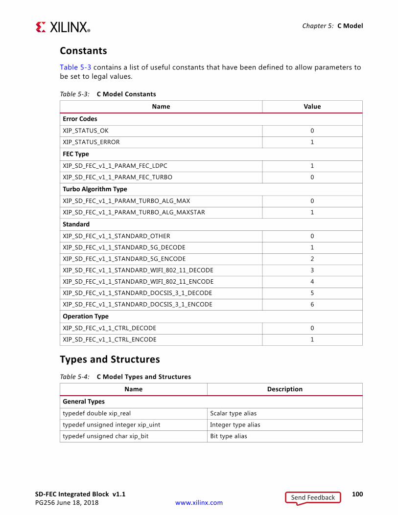
SD-FEC Integrated Block v1.1 100PG256 June 18, 2018 www.xilinx.com
Chapter 5: C Model
ConstantsTable 5-3 contains a list of useful constants that have been defined to allow parameters to be set to legal values.
Types and Structures
Table 5-3: C Model Constants
Name Value
Error Codes
XIP_STATUS_OK 0
XIP_STATUS_ERROR 1
FEC Type
XIP_SD_FEC_v1_1_PARAM_FEC_LDPC 1
XIP_SD_FEC_v1_1_PARAM_FEC_TURBO 0
Turbo Algorithm Type
XIP_SD_FEC_v1_1_PARAM_TURBO_ALG_MAX 0
XIP_SD_FEC_v1_1_PARAM_TURBO_ALG_MAXSTAR 1
Standard
XIP_SD_FEC_v1_1_STANDARD_OTHER 0
XIP_SD_FEC_v1_1_STANDARD_5G_DECODE 1
XIP_SD_FEC_v1_1_STANDARD_5G_ENCODE 2
XIP_SD_FEC_v1_1_STANDARD_WIFI_802_11_DECODE 3
XIP_SD_FEC_v1_1_STANDARD_WIFI_802_11_ENCODE 4
XIP_SD_FEC_v1_1_STANDARD_DOCSIS_3_1_DECODE 5
XIP_SD_FEC_v1_1_STANDARD_DOCSIS_3_1_ENCODE 6
Operation Type
XIP_SD_FEC_v1_1_CTRL_DECODE 0
XIP_SD_FEC_v1_1_CTRL_ENCODE 1
Table 5-4: C Model Types and Structures
Name Description
General Types
typedef double xip_real Scalar type alias
typedef unsigned integer xip_uint Integer type alias
typedef unsigned char xip_bit Bit type alias
Send Feedback

SD-FEC Integrated Block v1.1 101PG256 June 18, 2018 www.xilinx.com
Chapter 5: C Model
Dynamic ArraysThe C model represents input and output data using multi-dimensional dynamic arrays. The xip_array_<type> structure is used to specify a multi-dimensional dynamic array containing elements of type xip_<type>. Several utility functions are provided that allow creation, allocation and destruction of array instances.
For each array type, the DECLARE_XIP_ARRAY(<type>) macro can be used to declare the structure and utility function prototypes. The C model header already contains declarations for the xip_array_real and xip_array_bit array types used by the SD-FEC C model.
Dynamic Array Structure
The xip_array_<type> structure is used to specify a multi-dimensional array of data with type <type>. The content is summarized in Table 5-5.
Handler Function Signatures
typedef void (*xip_msg_handler)(void*handle, int error,const char* msg) Interface to a message handler function
Structures
typedef struct xip_sd_fec_v1_1_configModel configuration structure, fields:name: String identifier for model instance.fec: FEC code to be used. 0=LDPC, 1=Turbo.
typedef struct xip_sd_fec_v1_1_imp xip__v1_1 Handle type to refer to an instance of the model
typedef xip_uint xip_sd_fec_v1_1_ldpc_sc_table See Table 2-53 for field details.
typedef struct xip_sd_fec_v1_1_ldpc_la_table See Table 2-54 for field details.
typedef struct xip_sd_fec_v1_1_ldpc_qc_table See Table 2-55 for field details.
typedef struct xip_sd_fec_v1_1_ldpc_parameters See LDPC Code Parameters for field details.
typedef struct xip_sd_fec_v1_1_td_parameters See Table 2-48 for field details.
typedef struct xip_sd_fec_v1_1_ctrl_packet See Control AXI4-Stream Slave for field details
typedef struct xip_sd_fec_v1_1_stat_packet See Status AXI4-Stream Master for field details
Array Types
typedef struct xip_array_real Dynamic array, used for soft value input/output
typedef struct xip_array_bit Dynamic array, used for hard output
Table 5-5: C Model Dynamic Array Structure
Field Name Type Description
data xip_<type>* Pointer to array of data
data_size size_t Current number of elements in the data array
Table 5-4: C Model Types and Structures (Cont’d)
Name Description
Send Feedback

SD-FEC Integrated Block v1.1 102PG256 June 18, 2018 www.xilinx.com
Chapter 5: C Model
Dynamic Array Functions
Create Array
xip_array_<type>*xip_array_<type>_create();
This function allocates and initializes an empty array for holding values of type <type>. The function returns a pointer to the created structure, or null if the structure cannot be created. The structure fields are all initialized to zero indicating an empty array, with ownership associated with the xip_array_<type>_* functions.
Reserve Data Memory
xip_statusxip_array_<type>_reserve_data(xip_array_<type>* p,size_t max_nels);
This function ensures that array p has sufficient space to store up to max_nels elements of data. If the current data_capacity is insufficient and the current owner is zero, the function attempts to allocate or reallocate space to meet the request. The function returns XIP_STATUS_OK if the array capacity is now sufficient or XIP_STATUS_ERROR if memory could not be allocated.
Note: This function does not change the data or dimensions held within the array in any way; the contents of the array after calling the function are equivalent to the contents before calling the function, even if memory is reallocated. Also, this function never reduces memory allocation; use xip_array_<type>_destroy to release memory.
data_capacity size_t Max number of elements in the data array
dim size_t* Pointer to dimension array
dim_size size_t Current number of elements in the dimension array, dim
dim_capacity size_t Max number of elements in dim array
owner unsigned int
Ownership control. A value of 0 indicates that the structure and associated memory (for the data and dim fields) is allocated and owned by the xip_array_<type>_* functions, in which case the model can automatically resize arrays as required. Any other value indicates that the memory is owned by the user, and the model must report an error if an array is of insufficient capacity.
Table 5-5: C Model Dynamic Array Structure (Cont’d)
Field Name Type Description
Send Feedback

SD-FEC Integrated Block v1.1 103PG256 June 18, 2018 www.xilinx.com
Chapter 5: C Model
Reserve Dimension Memory
xip_statusxip_array_<type>_reserve_dim(xip_array_<type>* p,size_t max_nels);
This function ensures that array p has sufficient space to store up to max_ndims dimensions. If the current dim_capacity is insufficient and the current owner is zero, the function attempts to allocate or reallocate space to meet the request. The function returns XIP_STATUS_OK if the array capacity is now sufficient or XIP_STATUS_ERROR if memory could not be allocated.
Note: This function does not change the data or dimensions held within the array in any way; the contents of the array after calling the function are equivalent to the contents before calling the function, even if memory is reallocated. Also, this function never reduces memory allocation; use xip_array_<type>_destroy to release memory.
Destroy Array
xip_array_<type>*xip_array_<type>_destroy(xip_array_<type>* p);
This function attempts to release all memory associated with array p. If the owner field is zero, the function releases the memory associated with data, dim and p, and returns null indicating success. If owner is non-zero the function returns p, indicating failure.
FunctionsDetails of the C model functions are provided in the sd_fec_v1_1_bitacc_cmodel.h header file. Table 5-6 summarizes the C model functions.
Table 5-6: C Model Functions
Name Description
xip_sd_fec_v1_1_get_version Get version of C model library
xip_sd_fec_v1_1_create Create a new instance of the model
xip_sd_fec_v1_1_reset Reset an instance of the model
xip_sd_fec_v1_1_set_config_params Set/change configuration parameters
xip_sd_fec_v1_1_gen_ldpc_spec Generate LDPC specification file from parity check matrix (H).
xip_sd_fec_v1_1_gen_parity_check_mat
Generate parity check matrix (H) from LDPC specification file.
xip_sd_fec_v1_1_gen_ldpc_params Generate LDPC parameters from code specification.
xip_sd_fec_v1_1_add_ldpc_params Add an LDPC code to an instance of the model.
xip_sd_fec_v1_1_get_num_ldpc_codes Returns the number of LDPC codes added to the model instance.
Send Feedback
SD-FEC Integrated Block v1.1 104PG256 June 18, 2018 www.xilinx.com
Chapter 5: C Model
CompilingCompilation of user code requires access to the sd_fec_v1_1_bitacc_cmodel.h and xip_common_bitacc_cmodel.h header files. The header files should be copied to a location where they are available to the compiler. Depending on the location chosen, the 'include' search path of the compiler might need to be modified.
The sd_fec_v1_1_bitacc_cmodel.h header file includes the xip_common_bitacc_cmodel.h header file, so this does not need to be explicitly included in source code that uses the C model.
LinkingTo use the C model, the user executable must be linked against the correct libraries for the target platform.
Linux
The executable must be linked against the following shared object library:
• libIp_sd_fec_v1_1_bitacc_cmodel.so
Using GCC, linking is typically achieved by adding the following command line options:
-L. -Wl,-rpath,. -lIp_sd_fec_v1_1_bitacc_cmodel
This assumes the shared object libraries are in the current directory. If this is not the case, the -L. option should be changed to specify the library search path to use.
Using GCC, the provided example program run_bitacc_cmodel.c can be compiled and linked using the following command:
gcc -x c++ -I. -L. -lIp_sd_fec_v1_1_bitacc_cmodel -Wl,-rpath,. -o run_bitacc_cmodel run_bitacc_cmodel.c
An example compilation script, make_run_bitacc_cmodel.csh, is included in the zip file.
Windows
The executable must be linked against the following dynamic link library:
xip_sd_fec_v1_1_get_ldpc_params Returns the LDPC parameters for the specified control packet.
xip_sd_fec_v1_1_set_turbo_params Set Turbo parameters on an instance of the model.
xip_sd_fec_v1_1_process Process a code word/block.
Table 5-6: C Model Functions (Cont’d)
Name Description
Send Feedback
SD-FEC Integrated Block v1.1 105PG256 June 18, 2018 www.xilinx.com
Chapter 5: C Model
• libIp_sd_fec_v1_1_bitacc_cmodel.dll
Depending on the compiler, the import libraries might also be required:
• libIp_sd_fec_v1_1_bitacc_cmodel.lib
Using Microsoft Visual Studio, linking is typically achieved by adding the import libraries to the Additional Dependencies entry under the Linker section of Project Properties.
An example compilation script, make_run_bitacc_cmodel.bat, is included in the zip file.
ExampleThe run_bitacc_cmodel.c file contains example code to show the basic operation of the C model.
MATLAB InterfaceA MEX function and MATLAB software class are provided to simplify the integration with MATLAB. The MEX function provides a low-level wrapper around the underlying C model, while the class file provides a convenient interface to the MEX function.
CompilingSource code for a MATLAB MEX function is provided. This can be compiled in MATLAB by changing to the directory that contains the code and running the make_sd_fec_v1_1_bitacc_mex.m script.
InstallationTo use the MEX function, the compiled MEX function must be present on the MATLAB search path. This can be achieved in either of two ways:
1. Add the directory where the compiled MEX function is located to the MATLAB search path (see the MATLAB addpath function).
or
2. Copy the files to a location already on the MATLAB search path.
As with all uses of the C model, the correct C model libraries also need to be present on the platform library search path (PATH or LD_LIBRARY_PATH).
Send Feedback
SD-FEC Integrated Block v1.1 106PG256 June 18, 2018 www.xilinx.com
Chapter 5: C Model
MATLAB Non-Class InterfaceTable 5-7 defines the non-class functions provided by the MATLAB interface (the functions do not require a model instance object). These directly expose corresponding C model API functions.
Details of the function arguments can be found using the MATLAB help command.
MATLAB Class InterfaceThe @sd_fec_v1_1_bitacc class handles the create/destroy semantics on the C model. The class provides objects for each of the data, configuration and control structures, defined for the C model and described in Types and Structures.
Details of the function arguments can be found using the MATLAB help command.
Table 5-7: C Model MATLAB Non-Class Functions
Name Description
gen_ldpc_spec Generate LDPC specification file from parity check matrix (H).
gen_parity_check_mat Generate parity check matrix (H) from LDPC specification file.
Table 5-8: C Model MATLAB Class Function
Name Description
get_version Get version of library
reset Resets the model
set_config_params Set/change configuration parameters
add_ldpc_params Add an LDPC code to an instance of the model.
set_turbo_params Set Turbo parameters on an instance of the model.
process Process a code word/block.
Send Feedback
SD-FEC Integrated Block v1.1 107PG256 June 18, 2018 www.xilinx.com
Chapter 6
Example DesignThere are two example designs available. By default, the SD-FEC core generates a simulation-only example design, containing the IP instance and an example test bench. The default example design should not be used for synthesis/implementation as it contains only the IP instance.
An optional processor (PS)-based example design can be selected during IP customization; see Example Design Tab for more information. The PS example design can be used to generate a bitstream.
When generated, to open the example design, right-click on the IP instance in the project manager and select Open Example Design.
Simulation-Only Example DesignThe IP example test bench <component_name>_tb, instantiates the IP instance and drives each AXI4-Stream interface with stimulus. When the AXI4-Lite parameter interface is exposed, this is programmed with the configuration specified for the IP instance.
The interface traffic is supplied to the test bench using two transaction logs (one each for the AXI4-Stream interfaces, and the AXI4-Lite parameter interfaces). The transaction logs are output during example design generation and contain stimulus specific to the IP instance. They are added to the example design project. AXI4-Stream transaction logs can also be produced using the C Model example application, allowing further stimulus to be defined. The transaction logs contain traffic for one block per LDPC code, defined during customization, up to a maximum of three blocks. The order corresponds to the order in which the codes are defined during customization. See the LDPC Code Analysis Tab for code enumeration.
Send Feedback

SD-FEC Integrated Block v1.1 108PG256 June 18, 2018 www.xilinx.com
Chapter 6: Example Design
Processor-Based Example DesignThe Processor Subsystem (PS)-based example design builds a demonstration system implementing a bit error rate (BER) tester, including the capability to measure throughput and latency. An example processor application is also generated, and (optionally) compiled, which sets up and controls the BER test and demonstrates how to configure the SD-FEC IP core using the low-level bare-metal driver (Appendix C, SD-FEC Low-Level Bare-Metal Driver).
X-Ref Target - Figure 6-1
Figure 6-1: Example Test Bench
Core Instance – DUTS_AXI
S_AXIS_CTRL
S_AXIS_DIN_WORDS
S_AXIS_DOUT_WORDS
S_AXIS_DIN
AXI4-StreamSink
M_AXIS_STATUS
M_AXIS_DOUT
AXI4-LiteSource
AXI4-StreamSource
AXI4-StreamSource
AXI4-StreamSource
AXI4-StreamSource
AXI4-StreamSink
<component_name>_tb
Send Feedback

SD-FEC Integrated Block v1.1 109PG256 June 18, 2018 www.xilinx.com
Chapter 6: Example Design
Hardware
Overview
The system implements an AWGN (Additive White Gaussian Noise) channel supporting BPSK, QPSK, QAM-16 & QAM-64 modulation. It includes an optional encoder IP instance and additional monitoring blocks to measure the throughput and latency of both the encoder and decoder IP instances.
The design uses three clocks; the processor clock (100 MHz), the system clock (300 MHz) and SD-FEC IP clock (667 MHz).]
X-Ref Target - Figure 6-2
Figure 6-2: Block Diagram
X20568-032618
Send Feedback

SD-FEC Integrated Block v1.1 110PG256 June 18, 2018 www.xilinx.com
Chapter 6: Example Design
Data Source: Random data and control packet generation. Produces 128-bits of source data per output transaction at the system clock rate.
Source Data FIFO: Buffers source data (K-bits) to be consumed by the Statistics block, 16k x 128-bits.
Encoded Data FIFO: Buffers encoded data (N-bits) prior to modulation, 32k x 96-bits.
Modulation & Channel: Implements QAM modulation and the AWGN channel. The block accepts encoded hard bits at 96-bits per input transaction at the system clock rate. It outputs 4 x I/Q symbols at the system clock rate, giving a maximum channel throughput of 4 x 6-bits (QAM-64) x 300 MHz = 7.2 Gb/s.
Demodulation: Implements a Log-likelihood Ratio (LLR) demodulator. It also outputs hard bits used to determine the channel error.
Statistics: Calculates the channel & uncorrected bit & block error rates plus a decoder iteration count.
Monitor: Monitors the AXI4-Stream data interfaces logging a time stamp for the first and last codeblock of a group. The monitor blocks uses the output of a shared counter for the time stamp values.
The Monitor blocks allow the system to measure the throughput and latency of the encoder and decoder IP instances. It should be noted that the encoder typically has a much higher throughput than the decoder. The encoded data FIFO allows some buffering of encoded data but if this becomes full the encoder IP is throttled. Therefore, to measure the throughput of the encoder the number of codeblocks run through the system should be limited such the encoded data FIFO does not fill.
Parameters
The hardware design supports the configuration parameters in Table 6-1. These are set by the example application.
Table 6-1: Example Design Parameters
Parameter Description
non-5G NR Control
Code Selects the LDPC code ID to be used or the Turbo Decode block size
5G Control(1)
z_j Lifting factor
z_set Base graph cyclic shift set
bg Base graph
mb Number of parity bits
Send Feedback

SD-FEC Integrated Block v1.1 111PG256 June 18, 2018 www.xilinx.com
Chapter 6: Example Design
The statistics in Table 6-2 are captured by the design.
sc_idx Scale factor index, only available when the Normalized Min-Sum algorithm has been specified.
Common Control
max_iter Specifies the maximum decode iterations
term_on_pass Specifies that decode should terminate on parity pass.
BER
num_blocks Specifies the number of codeblocks to run through the data path.
snr Specifies the AWGN signal-to-noise ratio (SNR), -12dB to 16dB quantized to Fix17_11.
mod_type
Modulation type:0 = BPSK1 = QPSK2 = QAM163 = QAM64
zero_dataSpecifies that the source data should be all zeros, rather than randomized data. Note, when the encoder instance has not been included in the design it always uses zero data.
skip_channel Specifies that no channel noise should be applied.
Notes: 1. See Control AXI4-Stream Slave for more details.
Table 6-2: Example Design Statistics
Statistics Description
Statistics block
raw_berr Channel bit error count
raw_blerr Channel block error count
cor_berr Uncorrected bit error count after Decode
cor_blerr Uncorrected block error count after Decode
iter_cnt Decode iteration count
Monitor Blocks(1)
first Time stamp (counter value) of the last transaction (tlast = 1) of the first code block run through the system
last Time stamp (counter value) of the last transaction (tlast = 1) of the last code block run through the system
stalled The number of system clock cycles when the downstream IP has de-asserted tready causing the upstream IP to be throttled, that is, tvalid is High and tready is Low.
Notes: 1. Duplicated for each instance; encoder I/P, encoder O/P, decoder I/P and decoder O/P.
Table 6-1: Example Design Parameters (Cont’d)
Parameter Description
Send Feedback

SD-FEC Integrated Block v1.1 112PG256 June 18, 2018 www.xilinx.com
Chapter 6: Example Design
SoftwareThe example processor application is used to set up and control the BER test hardware and demonstrates how to configure the SD-FEC IP instance(s) using the low-level bare-metal driver (Appendix C, SD-FEC Low-Level Bare-Metal Driver).
The application files are output to the sw directory within the example design project. A TCL script to generate the example application SDK project is also output during example design generation, and placed in the project root directory. This can be optionally run during example design generation by selecting the Build SDK Project option of the Example Design tab of the Vivado® IDE. The script can be run manually using the Xilinx® software command line tool, xsct:
xsct -no-ini build_ps_example_app.tcl
When the design is built using a MicroBlaze processor, the generated application binary file (ELF file) can be imported into the example design project and used to simulate the whole system. The following Vivado TCL commands import the generated ELF file into the example design project:
add_files -norecurse <ipinst>_ex.sdk/example_app/Release/example_app.elfadd_files -fileset sim_1 -norecurse <ipinst>_ex.sdk/example_app/Release/example_app.elfset_property SCOPED_TO_REF ps_example [get_files -all-of_objects [get_fileset sources_1] <ipinst>_ex.sdk/example_app/Release/example_app.elf]set_property SCOPED_TO_CELLS { microblaze_ps } [get_files -all-of_objects [get_fileset sources_1] <ipinst>.sdk/example_app/Release/example_app.elf]set_property SCOPED_TO_REF ps_example [get_files -all-of_objects [get_fileset sim_1] <ipinst>_ex.sdk/example_app/Release/example_app.elf]set_property SCOPED_TO_CELLS { microblaze_ps } [get_files -all-of_objects [get_fileset sim_1] <ipinst>_ex.sdk/example_app/Release/example_app.elf]
Note that if the Build SDK Project option has been selected these steps are done as part of the example design generation.
Send Feedback

SD-FEC Integrated Block v1.1 113PG256 June 18, 2018 www.xilinx.com
Chapter 6: Example Design
Application SummaryX-Ref Target - Figure 6-3
Figure 6-3: Application Flow Chart
X20497-030818
Send Feedback

SD-FEC Integrated Block v1.1 114PG256 June 18, 2018 www.xilinx.com
Chapter 6: Example Design
The flow chart in Figure 6-3 shows the basic application behavior. The detail of the application varies depending on the configuration specified for the SD-FEC IP and example design. By default the application has the NO_IO macro defined which disables interactive functionality. The macro should be removed to enable the stdin and stdout functionality.
The SDK project is configured to use the MicroBlaze™ Debug Module or CoreSight Debug for stdin & stdout as the hardware design does not include a separate UART device or enable the PS UART.
When the interactive functionality is enabled all the design parameters, defined in Table 6-1, can be updated using the UART terminal. A basic menu system is implemented where the parameters can be updated and repeated tests run.
Send Feedback

SD-FEC Integrated Block v1.1 115PG256 June 18, 2018 www.xilinx.com
Appendix A
UpgradingThis appendix is not applicable for the first release of the core.
Send Feedback
SD-FEC Integrated Block v1.1 116PG256 June 18, 2018 www.xilinx.com
Appendix B
DebuggingThis appendix includes details about resources available on the Xilinx® Support website and debugging tools.
Finding Help on Xilinx.comTo help in the design and debug process when using the SD-FEC, the Xilinx Support web page contains key resources such as product documentation, release notes, answer records, information about known issues, and links for obtaining further product support.
DocumentationThis product guide is the main document associated with the SD-FEC. This guide, along with documentation related to all products that aid in the design process, can be found on the Xilinx Support web page or by using the Xilinx® Documentation Navigator.
Download the Xilinx Documentation Navigator from the Downloads page. For more information about this tool and the features available, open the online help after installation.
Technical SupportXilinx provides technical support at the Xilinx Support web page for this LogiCORE™ IP product when used as described in the product documentation. Xilinx cannot guarantee timing, functionality, or support if you do any of the following:
• Implement the solution in devices that are not defined in the documentation.
• Customize the solution beyond that allowed in the product documentation.
• Change any section of the design labeled DO NOT MODIFY.
To contact Xilinx Technical Support, navigate to the Xilinx Support web page.
Send Feedback

SD-FEC Integrated Block v1.1 117PG256 June 18, 2018 www.xilinx.com
Appendix B: Debugging
Debug ToolsThere are many tools available to address SD-FEC design issues. It is important to know which tools are useful for debugging various situations.
Vivado Design Suite Debug FeatureThe Vivado® Design Suite debug feature inserts logic analyzer and virtual I/O cores directly into your design. The debug feature also allows you to set trigger conditions to capture application and integrated block port signals in hardware. Captured signals can then be analyzed. This feature in the Vivado IDE is used for logic debugging and validation of a design running in Xilinx devices.
The Vivado Logic Analyzer is used with the logic debug IP cores, including:
• ILA 2.0 (and later versions)
• VIO 2.0 (and later versions)
See the Vivado Design Suite User Guide: Programming and Debugging (UG908) [Ref 7].
Send Feedback
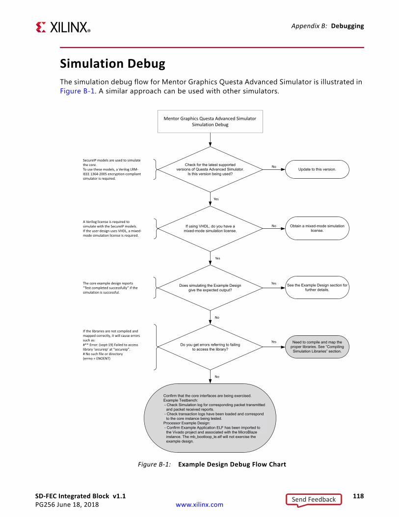
SD-FEC Integrated Block v1.1 118PG256 June 18, 2018 www.xilinx.com
Appendix B: Debugging
Simulation DebugThe simulation debug flow for Mentor Graphics Questa Advanced Simulator is illustrated in Figure B-1. A similar approach can be used with other simulators.
X-Ref Target - Figure B-1
Figure B-1: Example Design Debug Flow Chart
Mentor Graphics Questa Advanced SimulatorSimulation Debug
No
No
Yes
Yes
Yes
Yes
No
No
SecureIP models are used to simulate the core.To use these models, a Verilog LRM-IEEE 1364-2005 encryption-compliant simulator is required.
A Verilog license is required to simulate with the SecureIP models.If the user design uses VHDL, a mixed-mode simulation license is required.
The core example design reports “Test completed successfully” if the simulation is successful.
If the libraries are not compiled and mapped correctly, it will cause errors such as:#** Error: (vopt-19) Failed to access library ‘secureip’ at “secureip”.# No such file or directory(errno = ENOENT)
Send Feedback

SD-FEC Integrated Block v1.1 119PG256 June 18, 2018 www.xilinx.com
Appendix B: Debugging
Hardware DebugHardware issues can range from link bring-up to problems seen after hours of testing. This section provides debug steps for common issues. The Vivado debug feature is a valuable resource to use in hardware debug. The signal names mentioned in the following individual sections can be probed using the debug feature for debugging the specific problems.
General ChecksBy default, the SD-FEC core generates a simulation-only example design, containing the IP instance and an example test bench. The default example design should not be used for synthesis/implementation because it contains only the core instance.
• Ensure that all the timing constraints for the core were properly incorporated from the example design and that all constraints were met during implementation.
• Does it work in post-place and route timing simulation? If problems are seen in hardware but not in timing simulation, this could indicate a PCB issue. Ensure that all clock sources are active and clean.
• If using MMCMs in the design, ensure that all MMCMs have obtained lock by monitoring the locked port.
The core supports a BYPASS capability. This performs the same operation (so takes the same number of cycles, but without changing data between input and output).
Interface Debug
AXI4-Lite InterfacesWrite to one of the registers, (for example, Core Parameters register AXI_WR_PROTECT) and read back a value.
Read from a register that does not have all 0s as a default to verify that the interface is functional. Output s_axi_arready asserts when the read address is valid, and output s_axi_rvalid asserts when the read data/response is valid. If the interface is unresponsive, ensure that the following conditions are met:
• The s_axi_aclk and core_clk inputs are connected and toggling.
• The core is not in reset; reset_n is active-Low.
• If the simulation has been run, verify in simulation and/or a debug feature capture that the waveform is correct for accessing the AXI4-Lite interface.
Send Feedback

SD-FEC Integrated Block v1.1 120PG256 June 18, 2018 www.xilinx.com
Appendix B: Debugging
AXI4-Stream Interfaces• Check that all the interface clocks have been connected and are toggling, and that the
core is not held in reset (that is, reset_n is Low).
• Ensure interfaces are enabled (using Core Parameters AXIS_ENABLE Register (0x10)).
• If s_axis_din_tready output is Low ensure that a CTRL input and a DIN_WORDS input have been applied, and that the interfaces have been enabled over the AXI4-Lite parameter interface.
• If there is no output from DOUT (that is, s_axis_dout_tvalid is permanently Low) after a full block has been input on CTRL , DIN_WORDS and DIN, check that an input has been applied over the DOUT_WORDS interface.
• Check that the AXI4-Stream waveforms are being followed (see AXI4-Stream Interface).
• Check core configuration.
Send Feedback

SD-FEC Integrated Block v1.1 121PG256 June 18, 2018 www.xilinx.com
Appendix C
SD-FEC Low-Level Bare-Metal Driver
OverviewThe bare-metal API for the SD-FEC is described in this chapter. The driver is composed of the following files:
• API Interface
° xsdfec.c: The user interface API is implemented in this file.
° xsdfec.h: The user interface API prototypes are provided in this file. The file provides prototypes of the driver instance structure and all other structures used across the API.
° xsdfec_sinit.c: Device initialization functions.
• Hardware register map
° xsdfec_hw.h: Definitions for the hardware register maps and field masks are provided in this file.
• Device configuration
° x<ipinst_name>_turbo_params.h: Header file defining device/IP instance specific Turbo Decode configuration parameters derived from the hardware build. This file is only generated when an IP instance has been configured for Turbo Decode.
° x<ipinst_name>_<code_id>_params.h: Header file defining device/IP instance-specific LDPC configuration parameters derived from the hardware build; one header per specified LDPC code. This file is only generated when an IP instance has been configured for LDPC Decode or Encode.
Initialization and ConfigurationThe XSdFec_Config structure is used by the driver to configure the mode and interface parameters defined for the device. The configuration structure is created by the tool-chain based on hardware build properties.
Send Feedback
SD-FEC Integrated Block v1.1 122PG256 June 18, 2018 www.xilinx.com
Appendix C: SD-FEC Low-Level Bare-Metal Driver
The driver instance can be initialized in one of the following ways:
• XSdFecInitialize(InstancePtr, DeviceId) - The driver looks up its own configuration structure created by the tool-chain, based on an ID provided by the tool-chain.
• XSdFecCfgInitialize(InstancePtr, CfgPtr) - Uses a configuration structure provided by the caller.
One, or more, device-specific headers are produced during the generation of the board support package providing further configuration parameters.
When the device is configured for Turbo Decode the header, x<ipinst_name>_turbo_params.h, contains an xsd_fec_turbo_parameters structure populated to match the corresponding Vivado IDE configuration.
When the device is configured for LDPC, a header, per LDPC code specified on the corresponding Vivado IDE, is generated: x<ipinst_name >_<code_id>_params.h. Each header defines an xsd_fec_ldpc_parameters structure populated with the configuration data required for the corresponding LDPC code.
IMPORTANT: When the IP core has been configured to support the 5G NR standard, header files are not generated because the IP core directly supports the 5G NR codes.
The device-specific parameters can then be used to configure each SD-FEC device to match the hardware build.
Data StructuresAll the data structures used by the driver are defined in the xsdfec.h file.
struct XSdFec_ConfigDevice configuration information
u16 DeviceId // Device IDUINTPTR BaseAddress // Device base addressu32 Standard // Device standard u32 Initialization[4] // Device initialization
Send Feedback

SD-FEC Integrated Block v1.1 123PG256 June 18, 2018 www.xilinx.com
Appendix C: SD-FEC Low-Level Bare-Metal Driver
struct XSdFecDevice state information
UINTPTR BaseAddress // Device base addressu32 IsReady // Indicates IsReady following initializationu32 Standard // Device standardu32 SCOffset[128] // SC table offset lookup for each LDPC code ID, updated by XSdFecAddLdpcParamsu32 LAOffset[128] // LA table offset lookup for each LDPC code ID, updated by XSdFecAddLdpcParamsu32 QCOffset[128] // QC table offset lookup for each LDPC code ID, updated by XSdFecAddLdpcParams
struct XSdFecLdpcParametersLDPC parameters. See LDPC Code Parameters for full details.
u32 N // Number of codeword bits u32 K // Number of information bitsu32 Psize // Size of sub-matrixu32 NLayers // Number of layers in codeu32 NQC // Number of entries in the QC tableu32 NMQC // Specifies soft-data memory requirements u32 NM // Specifies soft-data memory requirementsu32 NormType // Normalization typeu32 NoPacking // QC operation packingu32 NoFinalParity // Skip final parityu32 MaxSchedule // Scheduling control parameteru32* SCTable // Pointer to scale table arrayu32* LDTable // Pointer to layer table arrayu32* QCTable // Pointer to QC table array
struct XSdFecTurboParametersTurbo Decode parameters. See Turbo Code Parameters for full details.
u8 Alg // Turbo algorithmu16 Scale // Turbo scale factor
struct XSdFecInterruptClassInterrupt classification and recovery action
u8 Intf // Triggered due to interface or control error (ISRu8 ECCSBit // Triggered due to single-bit ECC error (ECC_ISR)u8 ECCMBit // Triggered due to two-bit ECC error (ECC_ISR)u8 RstReq // Device requires reset u8 ReprogReq // Device requires LDPC codes reprogrammedu8 ReCfgReq // FPGA requires reprogrammed
Send Feedback
SD-FEC Integrated Block v1.1 124PG256 June 18, 2018 www.xilinx.com
Appendix C: SD-FEC Low-Level Bare-Metal Driver
User APIThe user API is implemented in the source file xsdfec.c. The prototypes for these are provided in header file xsdfec.h.
XSdFecInitialize
Function Prototype
int XSdFecInitialize(XSdFec *InstancePtr, u16 DeviceId);
Arguments
• XSdFec *InstancePtr: Pointer to device instance state structure.
• u16 DeviceId: ID of device to be initialized.
Description
Initializes the specified SD-FEC device and populates the device state structure. Combines XSdFecLookupConfig and XSdFecCfgInitialize.
Return Value
XST_SUCCESS
XST_FAILURE
Send Feedback

SD-FEC Integrated Block v1.1 125PG256 June 18, 2018 www.xilinx.com
Appendix C: SD-FEC Low-Level Bare-Metal Driver
XSdFecLookupConfig
Function Prototype
XSdFec_Config* XSdFecLookupConfig(u16 DeviceId);
Arguments
• u16 DeviceId: ID of device to look up.
Description
Returns the device configuration structure for the specified device.
Return Value
Pointer to device configuration.
XSdFecCfgInitialize
Function Prototype
int XSdFecCfgInitialize(XSdFec *InstancePtr, XSdFec_Config *ConfigPtr);
Arguments
• XSdFec *InstancePtr: Pointer to device instance state structure.
• XSdFec_Config *ConfigPtr: Pointer to device configuration structure.
Description
Initializes the SD-FEC device specified by the supplied configuration structure and populates the device state structure.
Return Value
XST_SUCCESS
XST_FAILURE
Send Feedback

SD-FEC Integrated Block v1.1 126PG256 June 18, 2018 www.xilinx.com
Appendix C: SD-FEC Low-Level Bare-Metal Driver
XSdFecSetTurboParams
Function Prototype
void XSdFecSetTurboParams(XSdFec *InstancePtr, const XSdFecTurboParameters* ParamsPtr);
Arguments
• XSdFec *InstancePtr: Pointer to device instance state structure.
• XSdFecTurboParameters* ParamsPtr: Pointer to Turbo parameter structure.
Description
Sets Turbo Decode parameters on the specified device instance.
Return Value
N/A
Send Feedback

SD-FEC Integrated Block v1.1 127PG256 June 18, 2018 www.xilinx.com
Appendix C: SD-FEC Low-Level Bare-Metal Driver
XSdFecAddLdpcParams
Function Prototype
void XSdFecAddLdpcParams(XSdFec * InstancePtr, u32 CodeId, u32 SCOffset, u32 LAOffset, u32 QCOffset, const XSdFecLdpcParameters* ParamsPtr);
Arguments
• XSdFec * InstancePtr: Pointer to device instance state structure.
• u32 CodeId: Code number to be used for the specified LDPC code
• u32 SCOffset: Scale table offset to use for specified LDPC code
• u32 LAOffset: LA table offset to use for specified LDPC code
• u32 QSCOffset: QC table offset to use for specified LDPC code
• XSdFecLdpcParameters* ParamsPtr: Pointer to LDPC code parameter structure.
Description
Updates LDPC code parameter registers and share tables using the specified CodeId and offsets with the specified parameters. The offsets arrays in the given XSdFec instance structure are updated with the supplied offsets for specified CodeId.
Note: When the device/IP has been configured to support the 5G NR standard the IP directly supports the 5G NR codes and it is not necessary to add the codes at run-time. This function generates an assertion if used on an instance configured to support the 5G NR standard.
Return Value
N/A
XSdFecShareTableSize
Function Prototype
void XSdFecShareTableSize(const XSdFecLdpcParameters* ParamsPtr, u32* SCSizePtr, u32* LASizePtr, u32* QCSizePtr)
Arguments
• XSdFecLdpcParameters* ParamsPtr: Pointer to parameters struct for the LDPC code being queried
• u32* SCSizePtr: Pointer to variable to populate with the effective scale table size for the specified LDPC code
Send Feedback

SD-FEC Integrated Block v1.1 128PG256 June 18, 2018 www.xilinx.com
Appendix C: SD-FEC Low-Level Bare-Metal Driver
• u32* LASizePtr: Pointer to variable to populate with the effective LA table size for the specified LDPC code
• u32* QCSizePtr: Pointer to variable to populate with the effective QC table size for the specified LDPC code
Description
Populates SCSizePtr, LASizePtr and QCSizePtr variables with the effective table size occupied by the specified LDPC code. These values can be used to increment the table offsets.
Return Vale
N/A
XSdFecInterruptClassifier
Function Prototype
XSdFecInterruptClass XSdFecInterruptClassifier(XSdFec *InstancePtr)
Arguments
• XSdFec * InstancePtr: Pointer to device instance state structure.
Description
Queries interrupt status registers and classifies interrupt and reports recovery action.
Return Value
Interrupt class structure defining interrupt class and recover action.
Send Feedback

SD-FEC Integrated Block v1.1 129PG256 June 18, 2018 www.xilinx.com
Appendix C: SD-FEC Low-Level Bare-Metal Driver
Base APISet and get functions are provided for all the individual registers and fields defined for the SD-FEC. The XSdFecAddLdpcParams abstract the configuration of an SD-FEC device but the main device control is done using the base API, for example, interface enablement and interrupt configuration. See Register Space and Designing with the Core for full details.
Note that the field level set functions use read-modify-write.
The base API functions take the following form.
Function Prototype
void XSdFecSet_<register_name>(UINTPTR BaseAddress, u32 Data);void XSdFecSet_<register_name>_<field_name>(UINTPTR BaseAddress, u32 Data);u32 XSdFecGet_<register_name>(UINTPTR BaseAddress);u32 XSdFecGet_<register_name>_<field_name>(UINTPTR BaseAddress);
Arguments
• XSdFec *InstancePtr: Pointer to device instance state structure.
• u32 data: Data to write to register or field.
Return Value
Value read from register or field
Interrupt HandlingThe SD-FEC low-level bare-metal driver does not implement any device-specific interrupt handling functions but does provide a helper function, XSdFecInterruptClassifier, to classify the interrupts once they have occurred and report the appropriate recovery action.
Generic interrupt handling routines should be used to service the interrupt(s) connected to the SD-FEC device(s) which can then call the XSdFecInterruptClassifier function to determine how to recover from the interrupt.
ExamplesThe processor-based example design output by the SD-FEC IP instance also includes an example application demonstrating a basic use case of the software driver. The following example is an extract from the example application.
Send Feedback

SD-FEC Integrated Block v1.1 130PG256 June 18, 2018 www.xilinx.com
Appendix C: SD-FEC Low-Level Bare-Metal Driver
Application#include "xsd_fec_dec_docsis_short_params.h" // Extract include below#include "xsd_fec_dec_docsis_medium_params.h"#include "xsd_fec_dec_docsis_long_params.h"
const unsigned int NUM_LDPC_CODES = 3;const XSdFecLdpcParameters* dec_codes[NUM_LDPC_CODES] = {&xsd_fec_dec_docsis_short_params,&xsd_fec_dec_docsis_medium_params,&xsd_fec_dec_docsis_long_params
};
int main() {
// SD FEC instanceXSdFec dec;
// Initialize SD-FEC instance XSdFecInitialize(&dec, XPAR_SD_FEC_DEC_DEVICE_ID);
// Add LDPC code parameters XSdFecAddLdpcParams(&dec,0,0,0,0,dec_codes[0]);
// Set up SD-FEC core parameters XSdFecSet_CORE_ORDER(dec.BaseAddress,0); // In-order termination XSdFecSet_CORE_AXIS_ENABLE(dec.BaseAddress,63); // Enable all I/Fs return 0;
}
xsdfec_dec_docsis_short_params.hxsdfec_dec_docsis_short_params.h
#ifndef XSDFEC_DEC_DOCSIS_SHORT_PARAMS_H#define XSDFEC_DEC_DOCSIS_SHORT_PARAMS_H#include "xsdfec.h"
const u32 xsd_fec_dec_docsis_short_sc_table_size = 2;u32 xsd_fec_dec_docsis_short_sc_table[2] = { 0x0000cccc, 0x0000000c};const u32 xsd_fec_dec_docsis_short_la_table_size = 5;u32 xsd_fec_dec_docsis_short_la_table[5] = { 0x00001007, 0x00001107, 0x00001008, 0x00001207, 0x00001007};const u32 xsd_fec_dec_docsis_short_qc_table_size = 82;u32 xsd_fec_dec_docsis_short_qc_table[82] = { 0x00020500, 0x00010000,
Send Feedback

SD-FEC Integrated Block v1.1 131PG256 June 18, 2018 www.xilinx.com
Appendix C: SD-FEC Low-Level Bare-Metal Driver
0x00020c02, … 0x00040e12, 0x00068113};XSdFecLdpcParameters xsd_fec_dec_docsis_short_params = { 0x00000460, // N 0x00000348, // K 0x00000038, // P 0x00000005, // NLayers 0x00000052, // NQC 0x0000002c, // NMQC 0x0000000a, // NM 0x00000001, // NormType 0x00000000, // NoPacking 0x00000000, // SpecialQC 0x00000000, // NoFinalParity 0x00000000, // MaxSchedule &xsd_fec_dec_docsis_short_sc_table[0], &xsd_fec_dec_docsis_short_la_table[0], &xsd_fec_dec_docsis_short_qc_table[0]};
#endif
Send Feedback

SD-FEC Integrated Block v1.1 132PG256 June 18, 2018 www.xilinx.com
Appendix D
Additional Resources and Legal Notices
Xilinx ResourcesFor support resources such as Answers, Documentation, Downloads, and Forums, see Xilinx Support.
Documentation Navigator and Design HubsXilinx® Documentation Navigator provides access to Xilinx documents, videos, and support resources, which you can filter and search to find information. To open the Xilinx Documentation Navigator (DocNav):
• From the Vivado® IDE, select Help > Documentation and Tutorials.
• On Windows, select Start > All Programs > Xilinx Design Tools > DocNav.
• At the Linux command prompt, enter docnav.
Xilinx Design Hubs provide links to documentation organized by design tasks and other topics, which you can use to learn key concepts and address frequently asked questions. To access the Design Hubs:
• In the Xilinx Documentation Navigator, click the Design Hubs View tab.
• On the Xilinx website, see the Design Hubs page.
Note: For more information on Documentation Navigator, see the Documentation Navigator page on the Xilinx website.
Send Feedback

SD-FEC Integrated Block v1.1 133PG256 June 18, 2018 www.xilinx.com
Appendix D: Additional Resources and Legal Notices
ReferencesThese documents provide supplemental material useful with this product guide:
1. AMBA AXI and ACE Protocol Specification (ARM IHI0022E)
2. Zynq UltraScale+ RFSoC Data Sheet: Overview (DS889)
3. Vivado Design Suite User Guide: Designing IP Subsystems using IP Integrator (UG994)
4. Vivado Design Suite User Guide: Designing with IP (UG896)
5. Vivado Design Suite User Guide: Getting Started (UG910)
6. Vivado Design Suite User Guide: Logic Simulation (UG900)
7. Vivado Design Suite User Guide: Programming and Debugging (UG908)
8. Vivado Design Suite User Guide: Implementation (UG904)
9. AMBA® AXI4-Stream Protocol Specification (ARM IHI 0051A)
10. Vivado Design Suite AXI Reference Guide (UG1037)
11. 3GPP TS 38.212 V15.0.0 3rd Generation Partnership Project; Technical Specification Group Radio Access Network; NR; Multiplexing and channel coding (Release 15) (http://www.3gpp.org/dynareport/38212.htm)
12. Data-Over-Cable Service Interface Specifications DOCSIS 3.1, Physical Layer Specification (https://apps.cablelabs.com/specification/CM-SP-PHYv3.1)
13. IEEE 802: Local and Metropolitan area Network Standards (http://standards.ieee.org/getieee802/download/802.11-2012.pdf)
14. 3GPP TS 36.212 V15.0.1;Evolved Universal Terrestrial Radio Access (E-UTRA); Multiplexing and channel coding (Release 15) (https://portal.3gpp.org/desktopmodules/Specifications/SpecificationDetails.aspx?specificationId=2426)
Send Feedback
SD-FEC Integrated Block v1.1 134PG256 June 18, 2018 www.xilinx.com
Appendix D: Additional Resources and Legal Notices
Revision HistoryThe following table shows the revision history for this document.
Please Read: Important Legal NoticesThe information disclosed to you hereunder (the “Materials”) is provided solely for the selection and use of Xilinx products. To the maximum extent permitted by applicable law: (1) Materials are made available “AS IS” and with all faults, Xilinx hereby DISCLAIMS ALL WARRANTIES AND CONDITIONS, EXPRESS, IMPLIED, OR STATUTORY, INCLUDING BUT NOT LIMITED TO WARRANTIES OF MERCHANTABILITY, NON-INFRINGEMENT, OR FITNESS FOR ANY PARTICULAR PURPOSE; and (2) Xilinx shall not be liable (whether in contract or tort, including negligence, or under any other theory of liability) for any loss or damage of any kind or nature related to, arising under, or in connection with, the Materials (including your use of the Materials), including for any direct, indirect, special, incidental, or consequential loss or damage (including loss of data, profits, goodwill, or any type of loss or damage suffered as a result of any action brought by a third party) even if such damage or loss was reasonably foreseeable or Xilinx had been advised of the possibility of the same. Xilinx assumes no obligation to correct any errors contained in the Materials or to notify you of updates to the Materials or to product specifications. You may not reproduce, modify, distribute, or publicly display the Materials without prior written consent. Certain products are subject to the terms and conditions of Xilinx’s limited warranty, please refer to Xilinx’s Terms of Sale which can be viewed at https://www.xilinx.com/legal.htm#tos; IP cores may be subject to warranty and support terms contained in a license issued to you by Xilinx. Xilinx products are not designed or intended to be fail-safe or for use in any application requiring fail-safe performance; you assume sole risk and liability for use of Xilinx products in such critical applications, please refer to Xilinx’s Terms of Sale which can be viewed at https://www.xilinx.com/legal.htm#tos.AUTOMOTIVE APPLICATIONS DISCLAIMERAUTOMOTIVE PRODUCTS (IDENTIFIED AS “XA” IN THE PART NUMBER) ARE NOT WARRANTED FOR USE IN THE DEPLOYMENT OF AIRBAGS OR FOR USE IN APPLICATIONS THAT AFFECT CONTROL OF A VEHICLE (“SAFETY APPLICATION”) UNLESS THERE IS A SAFETY CONCEPT OR REDUNDANCY FEATURE CONSISTENT WITH THE ISO 26262 AUTOMOTIVE SAFETY STANDARD (“SAFETY DESIGN”). CUSTOMER SHALL, PRIOR TO USING OR DISTRIBUTING ANY SYSTEMS THAT INCORPORATE PRODUCTS, THOROUGHLY TEST SUCH SYSTEMS FOR SAFETY PURPOSES. USE OF PRODUCTS IN A SAFETY APPLICATION WITHOUT A SAFETY DESIGN IS FULLY AT THE RISK OF CUSTOMER, SUBJECT ONLY TO APPLICABLE LAWS AND REGULATIONS GOVERNING LIMITATIONS ON PRODUCT LIABILITY.© Copyright 2018 Xilinx, Inc. Xilinx, the Xilinx logo, Artix, ISE, Kintex, Spartan, Virtex, Vivado, Zynq, and other designated brands included herein are trademarks of Xilinx in the United States and other countries. AMBA, AMBA Designer, Arm, ARM1176JZ-S, CoreSight, Cortex, PrimeCell, Mali, and MPCore are trademarks of Arm Limited in the EU and other countries.All other trademarks are the property of their respective owners.
Date Version Revision
06/18/2018 1.1 Placement Location Guidelines for SD-FEC IP Core updated.Runtime Loading Tab updated to include Physical Utilization and deprecated parameters.Link to SD-FEC Linux driver added to LogiCORE™ IP Facts Table notes.
04/30/2018 1.1 Updated document metadata.
04/04/2018 1.1 Initial Xilinx release.
Send Feedback


