116
November 2012 1
| Date post: | 14-Sep-2014 |
| Category: |
Business |
| View: | 649 times |
| Download: | 0 times |

November 2012 1

DISCLAIMER
This report was prepared as an account of work sponsored by an agency of the United States Government. Neither the United States Government, nor any agency thereof, nor any of their employees, nor any of their contractors, subcontractors, or their employees, makes any warranty, express or implied, or assumes any legal liability or responsibility for the accuracy, completeness, or usefulness of any information, apparatus, product, or process disclosed, or represents that its use would not infringe privately owned rights. Reference herein to any specific commercial product, process, or service by trade name, trademark, manufacturer, or otherwise, does not necessarily constitute or imply its endorsement, recommendation, or favoring by the United States Government or any agency, contractor, or subcontractor thereof. The views and opinions of authors expressed herein do not necessarily state or reflect those of the United States Government or any agency thereof.
Authors
Norman Bardsley Bardsley Consulting Stephen Bland SB Consulting Dan Chwastyk Navigant Consulting Caroline de Monasterio Navigant Consulting Lisa Pattison SSLS, Inc. Morgan Pattison SSLS, Inc. Fred Welsh Radcliffe Advisors, Inc. Mary Yamada Navigant Consulting

SSL Manufacturing Roadmap
SSL Manufacturing Roadmap S O L I D S T A T E L I G H T I N G R E S E A R C H A N D D E V E L O P M E N T
T A B L E O F C O N T E N T S
1 OVERVIEW OF SSL MANUFACTURING STATUS .......................................... 7 1.1 SSL Manufacturing Supply Chain .......................................................................... 8
1.1.1 LED-based SSL Manufacturing ......................................................................... 9 1.1.2 OLED-based SSL Manufacturing .................................................................... 10
1.2 Global and U.S. Production .................................................................................. 10 1.2.1 LED .................................................................................................................. 12 1.2.2 OLED ............................................................................................................... 15
1.3 DOE SSL Program ................................................................................................ 18 1.3.1 Program Elements ............................................................................................ 18 1.3.2 Cost Drivers ..................................................................................................... 19
2 LED PACKAGE AND LUMINAIRE ROADMAP .............................................. 30 2.1 LED Manufacturing Equipment ........................................................................... 30
2.1.1 Epitaxial Growth Equipment............................................................................ 30 2.1.2 Wafer Processing Equipment ........................................................................... 33 2.1.3 LED Packaging Equipment .............................................................................. 34 2.1.4 Luminaire and Module Assembly Equipment ................................................. 35 2.1.5 Test and Inspection Equipment ........................................................................ 36
2.2 LED Manufacturing Materials .............................................................................. 38 2.2.1 Substrate Materials ........................................................................................... 38 2.2.2 Chemical Reagents ........................................................................................... 41 2.2.3 Packaging Materials ......................................................................................... 41 2.2.4 Down-converter Materials ............................................................................... 43 2.2.5 Encapsulation Materials ................................................................................... 44
2.3 LED Die Manufacturing ....................................................................................... 45 2.3.1 Epitaxial Growth .............................................................................................. 45 2.3.2 Wafer Processing ............................................................................................. 46 2.3.3 Die Singulation ................................................................................................ 48
2.4 LED Package Manufacturing ................................................................................ 49 2.4.1 Die Packaging .................................................................................................. 49 2.4.2 Down-converter Application ............................................................................ 51 2.4.3 Encapsulation and Lensing .............................................................................. 51
2.5 LED Luminaire Manufacturing ............................................................................ 52 2.5.1 LED Die and Packages in Luminaires ............................................................. 52 2.5.2 Remote Phosphors ............................................................................................ 53

SSL Manufacturing Roadmap
2.5.3 Optical Component Manufacturing.................................................................. 54 2.5.4 LED Driver Manufacturing .............................................................................. 54 2.5.5 Luminaire Manufacturing ................................................................................ 56 2.5.6 Test and Inspection .......................................................................................... 58
2.6 LED Modeling and Simulation ............................................................................. 59 2.6.1 Cost Modeling .................................................................................................. 59 2.6.2 Design for Manufacturing ................................................................................ 60 2.6.3 Manufacturing Process Simulation .................................................................. 61 2.6.4 Luminaire Reliability Modeling ....................................................................... 62
2.7 LED Manufacturing Priority Tasks for 2013 ........................................................ 63
3 OLED PANEL AND LUMINAIRE ROADMAP ................................................. 66 3.1 OLED Manufacturing Equipment......................................................................... 67
3.1.1 Vacuum Processing Equipment ....................................................................... 68 3.1.2 Solution Processing Equipment ....................................................................... 70 3.1.3 Roll-to-Roll Processing Equipment ................................................................. 71 3.1.4 Encapsulation Equipment ................................................................................ 72
3.2 OLED Manufacturing Materials ........................................................................... 73 3.2.1 Organic Stack Materials ................................................................................... 73 3.2.2 Substrates ......................................................................................................... 75 3.2.3 Electrodes and Current Spreading Layers ........................................................ 77 3.2.4 Light Extraction Layers.................................................................................... 78 3.2.5 Integrated Substrates ........................................................................................ 79 3.2.6 Encapsulation ................................................................................................... 80
3.3 OLED Panel Manufacturing ................................................................................. 81 3.3.1 Process Integration ........................................................................................... 83 3.3.2 Process Control ................................................................................................ 83 3.3.3 Material Utilization .......................................................................................... 84 3.3.4 Manufacturing Yield ........................................................................................ 85 3.3.5 Manufacturing Costs ........................................................................................ 86
3.4 OLED Luminaire Manufacturing ......................................................................... 87 3.5 OLED Manufacturing Priority Tasks for 2013 ..................................................... 89
4 STANDARDS ........................................................................................................... 91 4.1 SSL Product Definitions ....................................................................................... 92 4.2 Minimum Performance Specifications ................................................................. 92 4.3 Characterization and Test Methods ...................................................................... 93
4.3.1 Reliability Characterization and Lifetime Definitions ..................................... 94 4.4 Standardized Reporting Formats........................................................................... 95 4.5 Interoperability and Physical Standards................................................................ 97 4.6 Process Standards and Best Practices ................................................................... 98

SSL Manufacturing Roadmap
APPENDIX A STANDARDS DEVELOPMENT FOR SSL ....................................... 99
APPENDIX B MANUFACTURING R&D PROJECTS .......................................... 104
APPENDIX C DOE SSL MANUFACTURING R&D TASKS ................................ 107
APPENDIX D REFERENCES .................................................................................... 108
T A B L E O F F I G U R E S
Figure 1.1 LED-based SSL Manufacturing Supply Chain ............................................................. 9 Figure 1.2 OLED-based SSL Manufacturing Supply Chain ........................................................ 10 Figure 1.3 Growth of LED Luminaire Sales by Region, 2011 to 2012 (26% overall) ................. 11 Figure 1.4 SSL Share of General Lighting Market for Lamps ..................................................... 11 Figure 1.5 LED Fab Capacity by Region (2013) .......................................................................... 14 Figure 1.6 Typical Cost Breakdown for an LED Package............................................................ 20 Figure 1.7 Projected LED Package Cost Reduction ..................................................................... 21 Figure 1.8 Comparison of Cost Breakdown for Different Types of Luminaires .......................... 22 Figure 1.9 A Comparison of Conventional and SSL Lighting Fixture Process Flows ................. 23 Figure 1.10 Cost Breakdown Projection for a Typical A19 Replacement Lamp ......................... 24 Figure 2.1 Veeco MaxBrightTM 14 x 100 mm Wafer Carrier ....................................................... 31 Figure 2.2 Veeco MaxBright MOCVD System ............................................................................ 32 Figure 2.3 Ultratech Sapphire 100 Stepper for LED Manufacturing............................................ 33 Figure 2.4 Improved Process Control Using Modern 150 mm Processing Equipment ................ 34 Figure 2.5 High Speed Moving Mirror Goniophotometer Model 6400 T by Lighting Sciences Inc. ................................................................................................................................................ 38 Figure 2.6 GaN-based LEDs on a 200 mm Silicon Wafer as Demonstrated by OSRAM ........... 39 Figure 2.7 Bulk GaN Substrates Produced by Sumitomo Electric Industries .............................. 40 Figure 2.8 Comparison of Typical High and Mid Power LED Packages Manufactured by Philips Lumileds ....................................................................................................................................... 42 Figure 2.9 Examples of LED Phosphors Available at Intematix Corp. ........................................ 44 Figure 2.10 Reduction in Relative Manufacturing Cost when Transitioning from 3” to 150 mm Diameter Wafers ........................................................................................................................... 47 Figure 2.11 Philips Lumileds Luxeon H50-2 High-Voltage LED Package ................................. 48 Figure 2.12 Example of Modularization in LED Package Manufacturing ................................... 50 Figure 2.13 Luxeon Z Package: (a) top view (monochromatic emitter), (b) rear view, and (c) top view (white emitter) ...................................................................................................................... 50 Figure 2.14 Philips A19 L•Prize Bulb .......................................................................................... 54 Figure 2.15 Schematic Representation of the Simple Modular LEDCOM Cost Model .............. 60 Figure 2.16 Integrated Systems Approach to SSL Manufacturing ............................................... 61 Figure 3.1 Desk Lamp with Color Tunable and Illuminance Variable OLED Panels – Solution Processed using Nozzle Printing Equipment ................................................................................ 70 Figure 3.2 Slot Coater Adapted for Coarse Patterning ................................................................. 71 Figure 3.3 Important Ink Characteristics in the Deposition of HIL and HTL Materials .............. 75

SSL Manufacturing Roadmap
Figure 3.4 Internal Extraction Structure with Laminated Plastic Film ......................................... 79 Figure 3.5 Tandem OLED Architecture ....................................................................................... 82 Figure 3.6 Schematic of In-Line Evaporation Process ................................................................. 84 Figure 3.7 Trilia OLED Luminaire by Acuity Brands .................................................................. 88 Figure 4.1 DOE Lighting Facts Label Example ........................................................................... 96 L I S T O F T A B L E S
Table 1-1 The LED Supply Chain: LED Die, Package, and Luminaire Manufacturers .............. 12 Table 1-2 The LED Supply Chain: Materials and Equipment Suppliers...................................... 13 Table 1-3 The OLED Supply Chain: Global Equipment and Materials Suppliers ....................... 16 Table 1-4 The OLED Supply Chain: Global Panel and Luminaire Producers ............................. 17 Table 1-5 The LED Supply Chain: Key Cost Drivers .................................................................. 25 Table 1-6 OLED Panel Cost Estimated Progress ($/m2) .............................................................. 27 Table 1-7 The OLED Supply Chain: Key Cost Drivers .............................................................. 29 Table 2-1 Epitaxy Metrics ............................................................................................................ 46 Table 3-1 Comparison of Current OLED Materials Cost against DOE Targets .......................... 86

SSL Manufacturing Roadmap
Page 1
EXECUTIVE SUMMARY
Key Findings and General Recommendations for 2013 In a recently-released Department of Energy (DOE) report by Navigant reviewing the adoption of solid state lighting (SSL) technology in the U.S. [1] the authors concluded that in 2012 LED lighting saved about 71 trillion British thermal units (BTUs) of primary energy amounting to about $675 million in cost savings for the end user. At this point, market penetration is quite modest. For one high-profile application, A-lamps, the authors estimate that less than one percent of total units deployed are LED-based lamps. But growth is accelerating rapidly as evidenced by a 26% increase in LED lighting product sales in one year, from 2011 to 2012 as reported by Strategies Unlimited [2]. The Navigant report further concluded that the 71 trillion BTU savings represents only a tiny fraction of the total potential energy savings of about 3.9 quadrillion BTU (quads) assuming complete adoption of SSL. While complete adoption may be a long ways off, the potential highlights the importance of developing a robust, high capacity manufacturing capability for SSL. Market adoption is likely to accelerate as prices continue to fall at rates of several tens of percent per year, and as it does, unit sales will increase at a much faster rate than revenues. DOE's SSL manufacturing initiative was begun in 2009 in response to this evident need to assist in the growth of production capability, the reduction of costs to promote adoption, and quality improvement - all aimed at achieving the overarching goal of maximized energy savings as soon as practicable. This is the fifth edition of the Manufacturing Roadmap which is intended to provide a guide to key manufacturing R&D priorities, to continue and improve capability and to establish a strong role for the U.S. in SSL production. Along the way, DOE has funded $46 million in manufacturing R&D projects directed at identified priorities. Some notable projects include KLA-Tencor’s development of the Candela 8620 inspection system [3], Veeco Instruments’ development of the MaxBrightTM MOCVD multi-reactor system [4], and GE Lighting’s development of advanced phosphor deposition methods [5]. As is evident from the examples, projects cover much of the value chain of SSL production, including not only process improvements but also manufacturing equipment, materials, testing, and designs for low cost. Further, projects include both the now rapidly expanding LED technology and also the still-nascent OLED lighting approach. To identify priority tasks appropriate for funding, DOE engages the SSL community beginning with a series of "round-table" discussions of invited experts to review the state-of SSL technology development and areas for improvement. This is followed by the annual SSL Manufacturing Workshop, which was held this June in Boston, MA [6]. The outcomes are summarized below and reflect a few key themes that arose during the discussions:
• LED manufacturing has benefited greatly from the rapid growth in LED-backlit displays. As a result, there is less of a need for attention on the basic LED chip manufacturing equipment and process. The most important needs are more specific to lighting.

SSL Manufacturing Roadmap
Page 2
• Luminaire manufacturing is changing dramatically in response to the new technology, with less emphasis on the lamp-fixture paradigm and increasing emphasis on integrated luminaires to minimize cost and maximize efficacy.
• Highly flexible luminaire and module manufacturing will be needed to address the rapidly expanding market. That is, to be able to accommodate the enormous variety of designs demanded by customers for multiple applications, lines will need to be efficient and cost-effective even with relatively low numbers for any given code. This may call for innovative methods and equipment.
• While there is potential for color-mixed solutions, much basic work remains to make that practical. The workhorse for current lighting products is phosphor-converted blue light, and there is still potential for energy improvement and cost reduction in that technology.
• The overriding barrier to adoption of OLED lighting is the high cost of OLED panels. Until that can be overcome, manufacturing efforts on OLED luminaires, while needed, may not be the highest priority.
• Although there is controversy about the appropriate scale, OLED deposition equipment is one place where some impact may be made. In particular there is a need for high yield processes and innovative approaches.
• Improvements in the materials supply for OLED manufacture represent an opportunity for cost reductions and increased performance, particularly in regards to integrated substrates and encapsulation.
Right now the biggest challenge for LED lighting is to expand to accommodate demand; the biggest challenge for OLEDs is to settle on an acceptable, cost-effective process and build demand. The expansion of LED lighting capacity, in order to be cost effective, will require innovative approaches to design and manufacturing; simple replication of existing capabilities is not sufficient. OLEDs need to translate some recent successes in efficacy and other performance parameters into cost-effective manufacturing, which is again likely to require novel approaches that go beyond what is being done in displays. Global Manufacturing Lighting is, and always has been, a global market. Today, just as SSL technology appears on the scene, very significant demand for lighting is growing throughout Asia in particular, but elsewhere as well. This, coupled with the rapid growth in LED backlighting for displays, has led to an explosion of LED wafer manufacturing capacity in Asia over the last few years (see figure on the following page) [7]. However, epitaxial capacity does not tell the whole story. Overall, in 2012, LEDs for lighting applications comprised about 23% of the total LED sales revenue [8], and there is a significant presence of LED makers for that market in North America. While most of this fabrication capacity does not apply to lighting, it does influence at least two important parts of the LED lighting supply chain: MOCVD equipment and the infrastructure that supports packaging of LEDs. Equipment is a significant market on its own, and provides a promising opportunity for North American companies. Packaging of LEDs has largely migrated to Asia, partly because of a strong existing semiconductor packaging infrastructure, but is also influenced by low-cost labor. Assembly of replacement lamps, built on a similar infrastructure, has also strengthened in Asia.

SSL Manufacturing Roadmap
Page 3
It remains to be seen what will happen with integrated luminaires. These products are larger and heavier than lamps or LED packages, and also tend to be more specialized by region. Accordingly, there is some incentive to develop local manufacturing capability for this segment of the value chain. There are, in fact, thousands of luminaire makers from the legacy technologies worldwide, many of which may not survive the transition to SSL. However, many will survive and new companies are appearing as the market grows – many of which have origins North America. Little can be said about the development of manufacturing of OLED lighting at this time because the market is just developing. However, driven by the demand for small OLED displays for portable devices, Asian companies, especially in Korea, have begun to make significant investment in OLED manufacturing. While OLED lighting will be quite different, these display investments will certainly have an influence on the market both in terms of equipment and materials costs. Currently, there is a high barrier to entry for OLED manufacturing which may discourage smaller companies from addressing this market. However, alternative, lower capital cost approaches are being explored for OLED panel manufacturing for lighting, and, if successful, may help to spur U.S. participation. OLED luminaires will be subject to similar considerations as LED luminaires as noted above. LED Manufacturing R&D Priorities During the Roundtables, Manufacturing Workshop, and internal DOE discussions, three Manufacturing R&D tasks for LED-based luminaire manufacturing were identified for 2013. These choices for LED Manufacturing are listed by title and brief descriptions are provided below.
M.L1 Luminaire Manufacturing Support for the development of flexible manufacturing of state of the art LED modules, light engines, and luminaires.
M.L3 Test and Inspection Equipment Support for the development of high-speed, high-capability, non-destructive test equipment with standardized test procedures and appropriate metrics.
M.L7 Phosphor Manufacturing and Application Development of efficient manufacturing and improved application of phosphors (including alternative down converters) used in solid state lighting.
OLED Manufacturing R&D Priorities There were two OLED Manufacturing R&D tasks identified for 2013 as a result of the same feedback mechanisms described for LEDs. The selections for the development of OLED manufacturing technology are listed below.

SSL Manufacturing Roadmap
Page 4
M.O1 OLED Deposition Equipment Support for the development of manufacturing equipment enabling high speed, low cost, and uniform deposition of state of the art OLED structures and layers.
M.O3 OLED Substrate and Encapsulation Manufacturing Support for the development of advanced manufacturing of low cost integrated substrates and encapsulation materials.
Overall Cost Projections and Contributions to Cost Reduction Since its inception, the DOE SSL manufacturing initiative has emphasized the importance of significantly reducing costs in order to speed adoption and the consequent energy savings. At this stage of the technology development, LED product prices have fallen sufficiently such that adoption has begun to accelerate rapidly, while OLED prices are still out of range for most buyers. LED Lighting LED package costs have benefited greatly from high volume manufacture for flat screen displays and televisions. While that market is cooling-off now, much of the learning, cost reduction, as well as the available capacity, is having a direct impact on the costs of LED packages for lighting. Current prices are around $5/klm for cool white and around $6/klm for warm [9]. These falling LED prices have had a major effect on replacement lamp costs which fell an estimated 28% from 2012 to 2013 as shown in the figure on the right. However, as LED prices continue to fall, LED packages will have a less dominant role in overall lamp and luminaire costs - about 45% of the A-lamp now, but expected to be less than 25% by 2020. As a result, continuing cost reduction will depend not so much on any one element of the bill of materials but rather on improvements in multiple categories. The specific results and impact are different for the various applications, but the trend and conclusion still apply. Principal cost drivers for LED luminaire products will migrate from LED package-oriented issues such as control of epitaxial processes and the development of cost-effective high throughput deposition to more luminaire-oriented issues such as automated assembly, code flexibility, streamlined testing, and system-oriented design for manufacture.
0.0
0.2
0.4
0.6
0.8
1.0
2012 2014 2016 2018 2020
Relative Cost for LED 800 lm A19 Lamp

SSL Manufacturing Roadmap
Page 5
OLED Lighting OLED lighting is in a different place. While there has recently been a dramatic expansion in the use of OLEDs for small displays, particularly in smartphones and small tablets, a direct impact on the cost of OLED lighting products is not yet evident. Partly this is because OLED lighting manufacturing is still evolving and the device architectures and performance requirements are different than those for displays. Further, the production scale is much smaller than for displays, so it cannot readily adopt either the experience or the equipment and infrastructure of display fabrication. The small scale and newness of the OLED lighting industry complicates cost projections which involve many assumptions not easily tested. It is, nonetheless, possible to envision a scenario whereby OLED lighting panels may achieve viable costs within the next decade or so. To achieve a cost of $100/m2 (corresponding to about $10/klm) will likely require several key assumptions and strategies, among them:
• OLED material costs will fall as the display market grows. • Initial manufacturing will need to be in relatively small substrate size in order to
minimize the capital outlay to make viable pricing possible. • Manufacturers must be able to provide high performance products at prices appropriate
for the intended market or application. • The moderate scale, small substrate manufacturing is an opportunity to devise
fundamental cost reductions of materials and processes. • Ultimately very low costs may only be achieved when volumes become large enough to
justify high-capital-cost larger scale equipment and low cost for high-performance materials.
The cost estimate shown in the figure above is not a target or prediction of where OLED costs may be in the next few years, but rather an indication of the kind of movement and action that may be necessary to realize a viable OLED lighting market. In fact, it may be necessary to accelerate these cost reductions by five years or so to realize substantial market shares and corresponding energy savings for OLEDs. Early cost drivers will be related to emitting and packaging materials inputs and the design of efficient small scale processes. Later, the design of cost-effective larger scale machines and packaging issues may become more significant. There may be other paths as well; this is just one example but all are likely to be similarly risky, and progress on OLED price reduction and sales volume has been very disappointing so far. A critical ingredient to success may be the willingness of the industry to, at this point, agree on a set of processes and design assumptions that will allow the players to move forward in concert towards a common goal.
10
100
1000
10000
100000
2010 2015 2020 2025
OLED Panel Cost Scenario $/m2

SSL Manufacturing Roadmap
Page 6
Since there is not a significant OLED luminaire market, we have not attempted to develop a cost reduction track for a full OLED luminaire. However, because of the very high cost of panels, they will dominate OLED luminaire costs for some time. Prices in the very near term will largely be driven by what the market will bear for highly decorative and specialized fixtures.

SSL Manufacturing Roadmap
Page 7
1 OVERVIEW OF SSL MANUFACTURING STATUS This document considers the manufacturing of solid state lighting (SSL) products. SSL involves the use of light emitting diodes (LEDs) or organic light emitting diodes (OLEDs) for the production of general illumination lighting. The manufacturing of LEDs, OLEDs, and SSL products has developed rapidly over the last two decades. Manufacturing developments have kept pace with technological developments enabling a large array of cost effective, high efficiency general illumination lighting products. This chapter provides a general status for the manufacturing supply chains for LED and OLED-based lighting as well as a general discussion of geographical production trends for SSL. While in some applications, such as A-type replacement lamps, SSL accounts for less than 1% of installations, for others it is beginning to be quite significant. According to a report from Navigant on adoption rates for LED lighting, LED lamps made up about 10% of MR16 type installations in 2012, and just under 5% of directional lamps. Market share is rapidly increasing. Due to its efficiency, reasonable cost of ownership, controllability, and lifetime, LED lighting has the potential to become the dominant lighting technology accounting for the majority of the lighting market within the next twenty years. This would represent a fundamental shift in the lighting market and require very rapid growth in SSL production capabilities. The manufacturing processes for LEDs and LED-based lighting products have quickly evolved into large-scale production processes. However, LED and LED-based lighting manufacturing is still developing compared to the manufacturing processes used for similar end products like semiconductor integrated circuits, consumer electronics, or conventional lighting fixtures. At this early stage in the maturation of LED-based SSL, while manufacturing approaches are still being refined, there is an opportunity to develop new manufacturing tools, materials, and techniques that can dramatically impact the cost and quality of LED-based lighting and define the manufacturing supply chain. The U.S. is currently well-positioned with respect to manufacturing equipment, which may assist in the development of a broader, well-defined, domestic manufacturing infrastructure that could provide long term domestic manufacturing jobs and other benefits. OLED-based SSL technology is much less developed than LED-based SSL. OLED lighting offers intriguing potential benefits in terms of cost and lighting performance. OLEDs are fundamentally large area, low brightness light sources which could complement high brightness, small area LED light sources. OLEDs also have the potential for low cost roll-to-roll (R2R) type production. However, OLED panel manufacturers are facing critical challenges in turning this promise into reality and demonstrating the benefits of this technology to luminaire manufacturers and potential customers. The greatest impediment to market acceptance of OLED lighting now is the extremely high cost of the available panels. The typical product has a light emitting area of about 100 cm2 and produces up to around100 lm at a price of roughly $100 or more. Furthermore, almost all of the panels are rigid with simple, planar shapes. Luminaire manufacturers are attempting to add value by embedding multiple panels into stylish fixtures, but this adds even more cost. The

SSL Manufacturing Roadmap
Page 8
resulting luminaires are acceptable only for applications in which the decorative value is more important than the light output. The development of OLED technology and manufacturing may be accelerated by the manufacturing and use of OLED displays in mobile devices, currently the largest market, as well as other developing applications such as television displays. While important differences in the technology and performance requirements could limit the applicability of OLED display developments to lighting production, advancements in OLED production technology could nevertheless greatly impact the performance and cost of OLED products and influence the geography and structure of the OLED supply chain.
1.1 SSL Manufacturing Supply Chain Both LED and OLED manufacturing processes can be generally defined by a sequence of reasonably independent manufacturing steps. These manufacturing steps are supported by the supply of manufacturing equipment, materials, and testing equipment. The combination of the manufacturing processes, equipment, materials, and testing constitute the manufacturing supply chain. This document refers to the manufacturing supply chains for LED and OLED-based SSL to discuss the cost, quality, and domestic manufacturing impacts. The supply chains shown below represent the general situation for LED and OLED-based SSL manufacturing right now, but these supply chains will continue to evolve and mature. For example, a vertically integrated manufacturer might currently handle a number of these processes internally, however as the manufacturing industry matures it is common for the supply chain to become more disaggregated for optimum manufacturing efficiency. In addition, the manufacturing supply chain will be impacted by developments in technology and product design and can also be impacted by product distribution including geographical or regulatory considerations.

SSL Manufacturing Roadmap
Page 9
1.1.1 LED-based SSL Manufacturing
Figure 1.1 LED-based SSL Manufacturing Supply Chain
Figure 1.1 is a schematic representation of the LED-based SSL manufacturing supply chain. The main manufacturing flow is described by the blue shaded boxes and blue arrows. The supporting elements of the supply chain are broken down into manufacturing equipment, materials, and test and measurement equipment. These supporting elements feed into the main manufacturing flow as indicated by the relevant arrows. The manufacturing process for LED-based luminaires begins with LED die manufacturing, consisting of growth of the LED wafer by metal organic chemical vapor deposition (MOCVD), processing of the LED wafer by mostly conventional semiconductor processes, and separation of the LED wafer into individual LED chips. The next step is packaging of the LED die into LED packages, including the deposition of phosphor material to convert the blue LED emission to white light. Finally, the LED packages are integrated into the end luminaire or lamp product. The luminaire also requires the integration of a driver, heat sink, optical components, and general mechanical structure.

SSL Manufacturing Roadmap
Page 10
1.1.2 OLED-based SSL Manufacturing
Figure 1.2 OLED-based SSL Manufacturing Supply Chain
Figure 1.2 is a schematic representation of the OLED-based SSL manufacturing supply chain. Similar to the LED version, the supply chain is broken down into a central manufacturing process flow with supporting equipment and materials. The OLED manufacturing process begins with the growth substrate. The growth substrate, typically glass, contains planarized transparent anode material and, possibly, current spreading grids and surface texturing on one or both surfaces for light extraction. The OLED stack is then deposited on the substrate with a metallic cathode. The OLED stack includes organic electron and hole charge conduction and emission materials. The next step is to encapsulate the OLED stack to protect the layers from degradation caused by oxygen or moisture. At this point the encapsulated OLED stack is typically referred to as a panel which can be directly integrated into a luminaire. Luminaire integration includes mechanically attaching the required number of OLED panels for the application and connecting a driver.
1.2 Global and U.S. Production SSL manufacturing is a truly global activity. An important objective for this and other government-supported R&D programs is that the economic benefit derived from such work benefits the U.S. economy to the greatest extent possible. Specifically for the SSL program, that objective translates to a desire to maintain a significant manufacturing role for the U.S. in the global lighting market. While, as Figure 1.3 shows, some fast-growing demand for SSL is in regions outside North America, there is nevertheless an opportunity to grow a long-term, domestic manufacturing infrastructure, especially for luminaires.

SSL Manufacturing Roadmap
Page 11
Figure 1.3 Growth of LED Luminaire Sales by Region, 2011 to 2012 (26% overall)
Source: Strategies Unlimited
The time for developing SSL manufacturing infrastructure is now, as SSL technology is projected to dominate the lighting market within 10 years, at least in terms of value. Figure 1.4 also shows that by 2020, LED light sources are projected to account for almost 50% of all lamp unit sales. This represents an enormous transition in the lighting market and demonstrates the opportunity for LED products in any type of lighting form factor.
Figure 1.4 SSL Share of General Lighting Market for Lamps
Source: McKinsey & Company, “Lighting the way”, First Edition, 2011

SSL Manufacturing Roadmap
Page 12
1.2.1 LED LED, lamp, and luminaire manufacturing are global enterprises with a global supply chain. Some geographical production trends can be identified but many of the input materials and semiconductor processing tools are produced worldwide. Table 1-1 and Table 1-2 highlight the global nature of SSL manufacturing by listing some of the key companies in each major geographical region involved in the manufacturing of LED-based SSL products and in the supply of equipment and materials to that market. It should be noted that these tables categorize geographical location based on company headquarter location and may not accurately reflect the balance of manufacturing activity. Table 1-1 The LED Supply Chain: LED Die, Package, and Luminaire Manufacturers
Supply Chain North America Europe Asia
Die Manufacturing
• Cree • Philips Lumileds • Bridgelux
• Soraa • SemiLEDs • Luminus Devices
• OSRAM Opto Semiconductors • Optogan • Plessey Semiconductors
• Nichia • Toyoda Gosei • Toshiba • Sharp • Epistar • TSMC
• OptoTech • FOREPI • Everlight • Lumens • Kingbright • Samsung
• LG Innotek • Seoul • Semiconductor • Sanan Optoelectronics
Package Manufacturing
• As above plus: • GE Lighting
• As above • As above plus: • Lite-On • Unity Opto • Lextar
Luminaire Manufacturing
• GE Lighting • Eaton/Cooper Lighting • Hubbell Lighting
• Acuity Brands • Cree • Lighting Science Group
• Philips • Osram Sylvania • Zumtobel
• Panasonic • Toshiba • Sharp • LG
• Samsung • Yankon • NVC Lighting Technology Corp • FSL

SSL Manufacturing Roadmap
Page 13
Table 1-2 The LED Supply Chain: Materials and Equipment Suppliers Supply Chain North America Europe Asia
Equ
ipm
ent S
uppl
iers
Epitaxial growth • Veeco Instruments • Aixtron • Taiyo Nippon Sanso Wafer processing
• Plasma-Therm • Lam Research • Ultratech
• JPSA • Temescal
• Oxford Inst. Plasma Tech • EV Group • SUSS MicroTec • Logitech
• Nikon Corp • Canon Inc. • Ushio Inc.
LED packaging • Palomar Tech • Nordson ASYMTEK • ASM Pacific Tech Luminaire assembly
• Speedline Tech • Conveyor Tech
• ASM Siplace • Assembleon
• Panasonic • Fuji Machines
• Nutek
Test and inspection
• KLA-Tencor • Cascade Microtech • Wentworth Labs • Orb Optronix • Rudolph Tech
• Lighting Sciences Inc. • Gamma Scientific • Radiant Zemax • Labsphere
• SphereOptics • Daitron • Optest • Nanometrics • Chroma
• Laytec • Bede • Bruker
• Cameca • SUSS MicroTec • Ismeca
• Quatek • Fittech Co • QMC
• Shibuya • Panasonic • Fujikom
Mat
eria
ls S
uppl
iers
Substrates • Rubicon • Silian • GT Advanced Tech • Cree • Kyma
• Monocrystal • Ammono • St. Gobain • Soitec
• Astek • STC • LG Siltron • Crystalwise Tech
• Air Water Inc. • TeraXtal • ProCrystal • Crystaland • Samsung
• Kyocera • Namiki • Mitsubishi Chem Corp • Hitachi Cable
Chemical reagents
• SAFC Hitech • Dow Electronic Materials • Air Products
• SAES Pure Gas • Pall Corporation
• AkzoNobel • Linde Industrial Gases • Air Liquide
• Showa Denko KK • Matheson Tri Gas
Packaging • Bergquist Company • Cambridge America • CofanUSA
• DuPont • Laird Tech / • Cookson Electronics
• Chin-Poon • Gia Tzoong • HolyStone • Iteq • Leatec
• Polytronics Tech • TA-I Tech • Tong Hsing • Univacco Tech • Taiflex
• Viking Tech • Zhuhai Totking • Denka • Kyocera • NRK
Phosphors/Down-converters
• Intematix • Dow Electronic Materials • Philips Lumileds (internal) • GE (internal)
• Phosphortech • QD Vision • Nanosys • Pacific Light Tech
• Merck • Osram (internal)
• Nichia (internal) • Mitsubishi Chemical Corp • Denka
Encapsulation • Momentive Performance • Materials (InvisiSil)
• NuSil • Dow Corning
• Wacker Chemie • (LUMISIL)
• Shin-Etsu

SSL Manufacturing Roadmap
Page 14
LED die manufacturing for SSL applications takes place all over the world but certain activities tend to be centered in specific geographical areas. Most of the top level manufacturers perform MOCVD epitaxial growth locally with respect to their headquarters; Philips Lumileds and Cree in North America, Osram Semiconductors in Europe, and Nichia in Japan. In North America, LED manufacturers Philips Lumileds and Cree are both within the top seven worldwide LED manufacturers by revenue [10] and it is notable that both Cree and Lumileds are primarily focused on the general illumination market unlike the other top seven LED companies who are more focused on LEDs for display applications. MOCVD growth of LED wafers is a manufacturing strength for North America. Wafer processing is often handled locally but is increasingly being transferred to facilities in Asia. In contrast, almost all LED die packaging is performed in Asia. Figure 1.5 shows the relative MOCVD LED production capacity (lighting and display applications) by geographic region. Another area of strength for North American manufacturing is production of tools and equipment for LED manufacturing and testing. The MOCVD crystal growth process for LEDs is the cornerstone of the entire LED manufacturing process. The world-wide market for MOCVD tools is dominated by two manufacturers: Aixtron in Europe and Veeco in North America. Due to the growth of the LED market, both companies have experienced exceptional growth over the last five years and continue provide the vast majority of all MOCVD equipment used for LED production. North American manufacturers also provide a meaningful portion of the specialty wafer processing, packaging, and test and inspection tools required for LED production. Companies such as Plasma-Therm, Ultratech, and KLA-Tencor provide equipment to LED manufacturers all over the world. Lamp and luminaire manufacturing is distributed world-wide. LED lamp manufacturing has sprouted up in North America, Europe, and Asia. Cree, Lighting Science Group, and Philips Lighting have developed LED lamp (bulb) manufacturing capabilities in North America. LED lamp manufacturing represents an opportunity for manufacturers to establish long term domestic manufacturing capabilities to supply the North American market and perhaps export products. Similar to incandescent light bulb manufacturing, LED lamp manufacturing is likely to be highly automated with limited labor content. For luminaires local manufacturers have historically dominated production. This situation is likely to continue since LED luminaires are designed for local building types and luminaires can be bulky, leading to high shipping costs. Luminaire manufacturing is another opportunity for the development of long term domestic manufacturing capabilities.
Source: SEMI Opto/LED Fab Forecast, Feb. 2013
Figure 1.5 LED Fab Capacity by Region (2013)

SSL Manufacturing Roadmap
Page 15
As the LED lighting market unfolds there is also the likelihood that manufacturing capacity will be developed in regions where there is strong demand for the products. This minimizes shipping costs and considerations from the government may encourage local production.
1.2.2 OLED The scale and location of OLED lighting production is not yet defined, however Korean manufacturers LG Display and Samsung Display have made large commitments to developing OLED displays. This development activity seems likely to encourage OLED lighting capacity in the same region. There are smaller lighting pilot production facilities in North America, Europe, and Asia. In Korea, LG Chem has announced a capacity of 72,000 100 x 100 mm OLED lighting panels per month and similar production capacity is estimated for the Philips and Osram pilot lines in Europe. The global extent of the whole supply chain can be assessed from Table 1-3 and Table 1-4. Note that these lists are incomplete and that some of these companies are still at the development stage and may not yet have commercial offerings.

SSL Manufacturing Roadmap
Page 16
Table 1-3 The OLED Supply Chain: Global Equipment and Materials Suppliers
Supply Chain North America Europe Asia E
quip
men
t Sup
plie
rs Vapor
deposition
• Applied Materials • Kurt Lesker • Trovato Mfg
• Aixtron • Beneq • Cambridge Nanotech
• Canon Tokki • GJM • Hitachi Zosen
• Jusung • SFA • SNU
• Sunic • Ulvac
Coaters and printers
• Dimatix • Kateeva • Novacentric
• nTact • Xenon Corp.
• Coatema • Roth & Rau
• Dai Nippon Screen • Seiko Epson
• Sung Am Machinery • Tazmo
• Tokyo Electron • Unijet
Encapsulation • Coherent • MBraun • Oxford Lasers
• Avaco • Wonik IPS
• YAS • Canon Tokki
• Ulvac
Test and inspection
• Colnatec • Radiant Zemax
• Laytec
Mat
eria
ls S
uppl
iers
Substrates • Alcoa • DuPont-Teijin • Guardian
• Corning • PPG
• ArcelorMittal • St. Gobain • Schott Glass
• Asahi Glass • LG Chem
• Nippon Electric Glass • Samsung-Corning
Active organic materials
• DuPont • Plextronics • PPG • UDC
• BASF • Cynora • Merck • Novaled • Solvay
• Aglaia • Cheil • Daejoo • Doosan • Dow Electro-Materials • Duksan Hi-Metal
• Hodogaya • Idemitsu Kosan • Jilin Optical • JNC/Chisso • LG Chem • Lumtech • eRay Opto
• Mitsubishi Chemical • Mitsui Chemical • Nippon Steel Sumikin • Nissan Chemical • RuiYuan • Sumitomo Chemical
Conductors • Cambrios • DuPont • Intrinsiq Materials
• Agfa • Heraeus
Encapsulation
• DuPont • 3M • UDC
• Delo • Henkel • SAES Getters • Sud-Chemie
• Cheil • Dynic • Tera-Barrier Films

SSL Manufacturing Roadmap
Page 17
Table 1-4 The OLED Supply Chain: Global Panel and Luminaire Producers
Supply Chain North America Europe Asia
Panels
• Moser Baer • OLEDWorks
• Astron-Fiamm • Osram • Philips • Fraunhofer COMEDD
• First O-Lite • Kaneka • Konica Minolta • Lumiotec • Mitsubishi Chemical
• NewView • Nippon Seiki • Panasonic-Idemitsu (PIOL) • Pioneer • Showa Denko
• Sumitomo Chemical • Toshiba • Visionox • LG Chem • Mitsubishi Pioneer (MPOL)
Luminaires
• Acuity • WAC Lighting • LiteControl
• Blackbody • Liternity • Osram • Philips • Tridonic
• Hanyoung • KwangMyung Lighting • Mitsubishi-Pioneer • NEC Lighting
• Verbatim • Visionox • Synqroa

SSL Manufacturing Roadmap
Page 18
DOE's program addresses two overarching objectives:
- Overcoming technical and design barriers to efficient, high quality solid state lighting, and - Establishing the foundations
for successful market introduction
Two North American companies have announced programs to produce OLED lighting panels. OLEDWorks in Rochester, NY expects to be in production before the end of 2013 and Moser Baer in Canandaigua, NY continues to develop their manufacturing process. Both companies believe that innovations in their manufacturing approaches are central to reaching acceptable manufacturing costs without relying on very large scale manufacturing. This is an important concept for the manufacturing of OLED lighting since the initial market for OLED products may be limited. The manufacturing of active OLED materials is spread across three continents and substantial new investments are being made in the required facilities, to serve both display and lighting applications. Major producers include DuPont and PPG in North America, BASF and Merck in Germany, Idemitsu Kosan and Sumation in Japan, and Dow Chemical and Duksan Hi-Metal in Korea. There are experienced equipment makers in these same four countries. However, the large capital investment required to make the deposition equipment for display applications and the uncertain size of the market for OLED lighting are causing apprehension amongst all of the tool makers. The market for small scale equipment suitable for R&D operations is still healthy and is being pursued successfully by North American manufacturers, such as Kurt J. Lesker Company and Trovato Manufacturing.
1.3 DOE SSL Program In the United States, lighting consumed about 18% of the total site electricity use in 2010, according to a recent DOE report [11]. A second DOE report also finds that SSL technology offers the potential to save 217 terawatt-hours (TWh), or about one-third of lighting site electricity consumption, by 2025 [12]. That savings in site consumption corresponds to about 2.5 quadrillion British thermal units (quads) of primary energy, which is approximately equal to the forecasted 2025 energy production from "other" renewable sources such as wind and solar, making SSL a significant contributor to energy supply issues by reducing the demand on energy resources [13].
1.3.1 Program Elements DOE has responded to this opportunity with the Solid State Lighting Program, providing direction and coordination of many efforts intended to advance the technology and to promote adoption (see Appendix B for more information). The DOE supports SSL technical advancement through R&D funding and supports adoption through market introduction programs such as Lighting Facts®. The DOE SSL Program recognizes that energy savings comes from the development and widespread adoption of energy efficient lighting technology. To address the development of energy efficient lighting technology, the DOE has supported ‘Core Technology Research’ and ‘Product Development’ R&D in solid-state lighting. Core Technology Research is the application of new scientific concepts to SSL technology to improve efficiency or lighting performance, such as the development of quantum dot down converters or the exploration of non-polar gallium nitride (GaN) LEDs.

SSL Manufacturing Roadmap
Page 19
Product Development describes the development of advanced, breakthrough products that can be either luminaires or sub-components in the manufacturing supply chain. A good example of a Product Development project that DOE has supported was the development of the hybrid luminaire concept by Philips Color Kinetics. This product used cool white emitting LEDs together with red emitting LEDs to provide warm white light with excellent color rendering. Manufacturing R&D focuses on research to improve the state of manufacturing for LED and OLED-based solid state lighting products in order to reduce cost and improve quality. There have been projects to improve the MOCVD epitaxial tools, develop wafer inspection equipment, improve phosphor deposition processes, and several more. Basic research is also supported by the DOE through the Office of Science and their Energy Frontier Research Centers (EFRCs) and both play a role in developing the new scientific concepts that can be applied to solid state lighting. The portion of the DOE SSL Program addressing Core Technology Research and Product Development is described in the annually updated DOE SSL Multi-Year Program Plan (MYPP). To advance widespread adoption of SSL technology, the DOE SSL Program has also supported market development activities. These activities include demonstration installations, testing and verification of performance claims, standards development, life-cycle assessment, and more. This work is described in the DOE SSL Market Development Support Plan. Finally, the DOE recognizes the need to address the primary technological barriers to the adoption of SSL products – manufacturing cost and product consistency. To address these issues the DOE provides support for SSL Manufacturing R&D. This support has the additional aim of creating and retaining manufacturing jobs in the U.S. The DOE SSL Manufacturing R&D effort is the topic of this document, the DOE SSL Manufacturing Roadmap. Together the MYPP, Market Development Support Plan, and Manufacturing Roadmap describe the breadth of activities that the DOE SSL Program undertakes to achieve the basic DOE mission of energy savings. For R&D, DOE supports a continuum of research from Basic Research (supported by the DOE Office of Science) to Core Technology Research, Product Development, and Manufacturing R&D. This R&D has not just supported the development of highly efficient light sources, but has supported advancements in cost and quality that have enabled SSL products to rapidly enter the lighting market and save significant amounts of energy. In addition, the SSL Market Development Support Activities have played a large role in providing consumer confidence is SSL technology through the various initiatives that have been supported.
1.3.2 Cost Drivers For SSL manufacturing, reducing the cost of the final product involves an understanding of the source of costs at each key stage in the manufacturing process, and requires careful attention to the design of the product and of the manufacturing process. LED Cost Drivers The typical cost breakdown for an LED package is shown in Figure 1.6 below. The data represents high volume manufacturing of 1 mm2 die on 100 mm diameter sapphire substrates and packaging of the die to produce high power warm white phosphor-converted LED lighting sources. The analysis was performed using the cost model described in Section 2.6.1. In this

SSL Manufacturing Roadmap
Page 20
model the yield for each process step defines the cost of that step and a cumulative overall wafer yield is calculated after each step to reflect the percentage of good product progressing to the next step or, in the case of the final step, the percentage of good product produced. Compared with 2012, the relative cost breakdown is largely unchanged although there is an overall cost reduction of around 25% which is primarily associated with reductions in raw materials costs.
Figure 1.6 Typical Cost Breakdown for an LED Package
Source: DOE SSL Roundtable and Workshop attendees Figure 1.6 indicates that a significant proportion of the cost remains concentrated in the die-level packaging stage. This result is not too surprising since the final product is a packaged die and there are many thousands of such die on each wafer (around 5,000 1 mm2 die on a 100 mm diameter substrate). Therefore, costs associated with die-level activities will tend to dominate and manufacturers will need to address die-level packaging processes or perform more of the packaging activities at a wafer level in order to realize the required cost reductions. Figure 1.7, on the following page, shows how the LED package cost elements may change over time, falling to about 17% of 2013 values by 2020.

SSL Manufacturing Roadmap
Page 21
Figure 1.7 Projected LED Package Cost Reduction
Source: DOE SSL Roundtable and Workshop attendees
There is plenty of room for innovation in this area and DOE anticipates many different approaches to cost reduction including:
• Increased equipment throughput, • Increased automation, • Improved testing and inspection, • Improved upstream process control,1 • Improved binning yield, • Optimized packages (simplified designs, lower cost materials, multichip, etc.), • Higher levels of component integration (hybrid or monolithic), and • Wafer scale packaging.
1 Wafer-level costs such as substrates, epitaxial growth, and wafer processing, comprise a smaller percentage of the
final device cost, but improvements here can have a significant impact on packaging costs and device performance (see Section 2.3).

SSL Manufacturing Roadmap
Page 22
The typical cost breakdown for a luminaire will vary depending on the application. Figure 1.8 shows a comparison of the cost breakdown for an outdoor area lamp, indoor downlight, and A19 replacement lamp. It is apparent that the relative costs for different lamp types can vary considerably, especially the cost of the LED package(s). It is apparent that the relative costs can vary considerably, especially the cost of the LED package(s). Comments received from roundtable and workshop attendees have suggested that overhead costs represent a significant cost element and should be included in the cost charts along with the bill of materials costs.
Figure 1.8 Comparison of Cost Breakdown for Different Types of Luminaires
Source: DOE SSL Roundtable and Workshop attendees
A comparison between conventional luminaire manufacturing and SSL luminaire manufacturing shown in Figure 1.9 illustrates a number of these hidden costs which will need to be considered. The overhead cost included in the cost charts therefore refers to manufacturing engineering, product development, documentation, packaging, in-line and compliance testing, shipping, and distribution. The retail price will include an additional sales margin of maybe 30 to 50%.

SSL Manufacturing Roadmap
Page 23
Figure 1.9 A Comparison of Conventional and SSL Lighting Fixture Process Flows Source: John Tremblay, OSRAM, SSL Manufacturing Workshop, Boston, MA, June 2013
For a specific luminaire type it is instructive to consider how the cost breakdown might change as a function of time. Figure 1.10 shows how the relative manufacturing cost for a common A19 60Watt (W) replacement lamp is expected to change between 2012 and 2020. The figure also provides a projection of how the cost breakdown is expected to change. It can be seen that the major change in the cost breakdown relates to the cost of the LED packages and driver which are anticipated to fall from around 35% and 15% respectively of the lamp cost in 2013 to around 25% and 10% respectively by 2020. As noted above and shown in Figure 1.8, relative costs vary widely among specific luminaire and lamp types, so it is not possible to project a generic luminaire cost breakdown. Nonetheless, for most types a factor of three of four reduction in relative cost is probably not an unrealistic expectation.

SSL Manufacturing Roadmap
Page 24
Figure 1.10 Cost Breakdown Projection for a Typical A19 Replacement Lamp
Source: DOE SSL Roundtable and Workshop attendees
While early on the cost of LED packages dominated the total lamp cost, as time progresses this will be less the case. At this point in time we are approaching a stage in which no single cost element will dominate and cost reduction will be achieved by focusing on optimization of the complete system rather than focusing on any specific cost element. The key cost drivers for each major element of the LED supply chain are summarized in Table 1-5, on the following page.

SSL Manufacturing Roadmap
Page 25
Table 1-5 The LED Supply Chain: Key Cost Drivers
Supply Chain Cost Drivers
Equipment Suppliers
Epitaxial growth • Uniformity • Throughput
• Reagent usage efficiency • In-situ monitoring/ Process control
Wafer processing • Throughput • Automation • Yield
LED packaging • Throughput • Flexibility (packaging materials and package types)
Luminaire assembly • Throughput • Automation • Chip scale packaging
Test and inspection • Throughput • Accuracy • Reproducibility
Materials Suppliers
Substrates • Diameter • Quality • Standardization
Chemical reagents • Quality/Purity • Bulk delivery systems • In-line purification
Packaging • Standardization • Plastic Packages
Downconverter • Quality/Efficiency • Consistency
• Stability (thermal and optical flux)
• Reliability
Encapsulation • Quality • Reliability • Stability (thermal and optical flux)
Die Manufacturing • In-line inspection/ Process Control
• Yield • Testing
• Throughput • Capital costs
Package Manufacturing • Modularization • In-line inspection/ Process control
• Labor content • Testing • Standardization
• Yield • Throughput
Luminaire Manufacturing • Automation/Labor content • In-line inspection/ Process control
• Testing (performance and compliance)
• Modularization • Throughput

SSL Manufacturing Roadmap
Page 26
OLED Cost Drivers With respect to OLED lighting, cost reduction remains the highest priority and greatest challenge. Since production of lighting panels has been so limited, it is useful to look at the experience with OLED panels for display applications. There has been very rapid growth in the scale of OLED manufacturing for displays over the past few years, with annual production rising to over one million square meters in 2012. However, most of the production has been by one company (Samsung) for one product type – the display in a smart phone. These are high-value products and the cost of a small panel is roughly $40 ($7,000/m2).The success of Samsung in making profits while selling phones with OLED displays has led other Asian companies to invest heavily in OLED manufacturing, leading to total capital investments of in excess of $10 billion per year. However, repeating this success with other products presents considerable challenges, mainly concerning cost rather than performance. For example, DisplaySearch estimates that the manufacturing cost of the OLED panel in a 55” TV, as produced by LG Display, is around $4,000 ($5,000/m2). The production of OLED panels for lighting has mostly been accomplished in lines with much less automation, leading to even higher costs per area. The price charged by panel manufacturers is $10,000/m2 or more, leading to luminaire prices in excess of $20,000/m2 or $2,000/klm. Predicted sales of OLED lighting panels in 2013 at $15 million correspond to a total area of less than 1,000 m2 [14]. Substantial cost reduction will be needed for commercial success in OLED TV and OLED lighting markets. Since 55” LCD TVs illuminated by LED backlights can now be purchased at retail for about $500, broad market penetration by any competing technology will require manufacturing costs less than $250/m2. If this were achieved, the corresponding cost for OLED lighting panels with a luminous emittance of 10,000 lm/m2 would be near $25/klm. The long term target of the DOE SSL Program for OLED panels is $10/klm, to allow for continued reduction in the cost of LED luminaires. So the cost of OLED TVs needs to be reduced by a factor of 20, and that of OLED lighting by 100. This has led to vigorous debate within the community about the level of synergy between these two applications. Some proponents of OLED lighting argue that the best way to reach the long-term cost targets is to leverage the advances that will come from the development of OLED televisions. Others believe that costs of approximately $10/klm cannot be reached via this route and that radically different methods are needed that will results in reductions on a shorter time scale. While the base technology is similar for OLED displays and lighting it is important to acknowledge that the two applications have different performance requirements and economics that can affect the choice of manufacturing approaches. Lighting requires much lower cost and higher efficacy to be competitive, so while a manufacturing approach may be suitable for displays it may not entirely cross over to lighting.

SSL Manufacturing Roadmap
Page 27
Some important factors for reducing the cost of manufacturing of OLED panels for televisions will also help to reduce costs for lighting. These include:
• Cost of organic materials, • Material utilization, • Production yield, and; • Desiccant-free encapsulation.
Additional cost reductions needed are more specific to lighting:
• Avoiding the use of photolithography, • Short process times, • Inexpensive substrate and cover, and; • Formation of light extraction enhancement layers.
Formation of the thin-film transistor (TFT) backplane and patterning of sub-pixels are not relevant for lighting. The cost of OLED panels can be broken down into three major segments, the integrated substrate, organic stack and assembly, which includes encapsulation and testing. To avoid the commitment of large amounts of capital on a high-risk venture, the contribution of each segment must be reduced substantially before large production lines are installed. The schedule for cost reduction, displayed in Table 1-6, is based upon presentations made by LG Chem, Philips, Moser Baer, OLEDWorks and input from the DOE SSL Workshops. The costs for the three segments are estimated for each constructed panel and are not adjusted for the yield of good panels. That factor is taken into account in the final row. The overhead cost includes manufacturing engineering, insurance, property taxes, product development, documentation, packaging, shipping, and distribution. Table 1-6 OLED Panel Cost Estimated Progress ($/m2)
2012 2013 2016 2020 2025 Integrated Substrate 500 250 150 40 20
Organic Deposition 1,400 600 250 70 30
Assembly and Test 600 350 200 50 20
Overhead2 500 300 100 20 10
Total (unyielded) 3,000 1,500 700 180 80
Yield of Good Product (%) 15 25 70 75 80
Total Cost 20,000 6,000 1,000 240 100
2 See Section 1.3.2 for a list of overhead costs included.

SSL Manufacturing Roadmap
Page 28
Note that the estimates in Table 1-6 represent industry averages. The division of costs between segments may vary substantially between companies, depending for example on the number of organic layers or the complexity of the extraction enhancement structures. Since luminaire production has been confined mainly to samples and demonstrations, it is too early to forecast the evolution of luminaire costs in high volume. The total cost of the luminaire is expected to be roughly twice that of the panel for purely functional lighting, but may be higher for decorative fixtures. The key cost drivers for each major element of the OLED supply chain are summarized in Table 1-7, on the following page.

SSL Manufacturing Roadmap
Page 29
Table 1-7 The OLED Supply Chain: Key Cost Drivers
Supply Chain Cost Drivers
Equipment Suppliers
Sealing • Seal integrity • Process time Evaporators • Deposition rate • Materials utilization • Capital cost Wet Coaters • Drying time • Patterning Luminaire Assembly • Modularization • Automation Test & Inspection • Throughput • Accuracy
Materials Suppliers
Substrates • Material selection • Surface condition Organic Stack • Sales volume • Efficacy • Lifetime Encapsulation • Increased sales volume • Elimination of desiccants Electrodes • Material selection • Patterning Extraction Structures • Processing yield • Performance
Panel Manufacturing • Yield • Throughput • Capital • Testing Luminaire Manufacturing • Panel price • Labor • Modularization • Testing

SSL Manufacturing Roadmap
Page 30
2 LED PACKAGE AND LUMINAIRE ROADMAP The LED luminaire manufacturing supply chain is shown schematically in Figure 1.1. The main manufacturing flow comprises LED die manufacturing followed by LED package manufacturing, leading to luminaire manufacturing. Various inputs are required to fuel the manufacturing ranging from LED manufacturing equipment through specialty materials to test and measurement equipment. Each element of the supply chain is described in more detail in the following sections along with an indication of the major participants and their geographical distribution.
2.1 LED Manufacturing Equipment The production of LED packages and luminaires involves the use of a wide range of specialized manufacturing equipment. The critical equipment requirements for each major manufacturing step are discussed in the following sections along with some consideration of the worldwide equipment manufacturing base. LED wafer fabrication facilities are located throughout the world and Semiconductor Equipment and Materials International (SEMI) produces a quarterly ‘Opto/LED Fab Forecast’ which provides information on capacities and projected construction and equipment spending for the next 18 months. [15] The manufacturing equipment landscape is continually evolving in order to satisfy the ever changing demands of the LED and luminaire manufacturers. Many manufacturers place a premium on low acquisition cost and have in the past tended to modify their own equipment. More recently the communication between equipment manufacturers and end-users has improved and the market better understands the requirements of the LED manufacturing industry and has begun to offer a more complete range of manufacturing equipment specifically designed to meet those needs. Successful equipment is most often characterized by a low cost of ownership (COO). COO is the total cost of producing a good part from a piece of equipment (see Section 2.6.1) and can be used to drive manufacturing equipment evolution to reduce the cost of production. To achieve a low COO the equipment must offer excellent repeatability and reproducibility leading to high process yields, low acquisition and operating costs, high throughput and high utilization. In general the Roundtable and Workshop participants anticipated a factor of two reduction in COO over a five year timescale.
2.1.1 Epitaxial Growth Equipment Epitaxial growth is of fundamental importance in the manufacturing process and is accomplished MOCVD. This is the only technology capable of growing the entire device structure including the complex low temperature nucleation layer, the thick GaN buffer, the multi-quantum well (MQW) active region, and p-GaN cap. The focus therefore remains on developing improved MOCVD growth equipment. Alternative growth methods such as hydride vapor phase epitaxy (HVPE) and physical vapor deposition (PVD) offer advantages over MOCVD in some limited

SSL Manufacturing Roadmap
Page 31
areas of application but have not gained traction in the manufacturing process. HVPE is able to deposit thick GaN layers at high growth rate and low cost, and is commonly used to produce GaN templates. PVD is currently being investigated as a low cost method for depositing an Alumina (AlN) nucleation layer on sapphire and silicon substrates. The main issues driving epitaxial growth equipment development are as follows:
• Wavelength uniformity and reproducibility- Achieving tighter control over the wavelength uniformity and reproducibility of the LED light emission is critical in order to improve color point consistency in the final product, optimize product yields, eliminate the need for binning, and reduce product costs. Similarly, the material quality and internal quantum efficiency (IQE) must continue to improve in order to achieve the target efficacy improvements. Both requirements will be met by improved equipment design, process optimization, and process control. One area where significant progress has been made at the equipment level is in monitoring and controlling the wafer bow. Wafer bow is caused by stresses during growth and creates non-uniform contact between the wafer and the carrier which results in non-uniform heating. The indium gallium nitride MQW active region composition is extremely sensitive to temperature, resulting in non-uniform wavelength emission. One elegant solution has been to create an advanced engineered wafer carrier where the shape of the pockets match the wafer bow at this critical stage in the growth process and provide uniform heating of the wafer. Wavelength uniformity can be significantly improved using this technique with the proportion of the wafer falling within a 5 nm bin rising from 73% to over 90% as reported previously by Veeco [16].
• Throughput (cycle and growth times)-
Large-capacity manufacturing equipment (typically up to 56 x 2”, 14 x 100 mm, 6 x 150 mm or 3 x 200 mm wafer capacity) capable of producing high quality material is readily available, and developments in cluster tool technology, offer the prospect of even higher throughputs and reductions in overall cost of ownership. Equipment design modifications and process improvements has allowed the GaN growth rate to reach 15-20 μm/hr, which essentially eliminates growth time issues for the thicker GaN layers. Nevertheless there remains a need to continue to improve equipment capacity and reduce growth cycles in order to lower the overall cost of ownership.
Figure 2.1 Veeco MaxBrightTM 14 x 100 mm Wafer Carrier

SSL Manufacturing Roadmap
Page 32
• In-situ monitoring and process control- The demanding reproducibility and uniformity requirements suggest the need for advanced process control measures in conjunction with sophisticated in-situ monitoring (especially wafer temperature) and accurate process modeling. Active temperature control at the wafer surface is of particular importance since temperature drives the growth process. Developments in the use of ultraviolet (UV) pyrometery to measure temperatures at the wafer surface rather than remotely via the carrier surface offer a more direct route to active control. Veeco has previously suggested that an improvement in run-to-run reproducibility from 2.33 to 1.4 nm could be possible [16]. Other in-situ tools, such as for monitoring wafer bow are routinely incorporated into most production reactors, although they are not generally used in active monitoring and control of the manufacturing process.
• Reagent usage-
High purity metalorganic alkyl sources and hydride gases are expensive. One of the major costs for the epitaxially grown wafer is associated with trimethylgallium (TMG) since a large amount of the material is used to produce an LED epitaxial structure. This is due to a usage efficiency of only 20-25%. Work is required at the equipment design level to improve the source efficiencies and reduce manufacturing costs.
A reduced COO for epitaxy equipment might be achieved in many different ways, such as increased throughput (reduced cycle times and/or increased capacity), lower capital cost, improved materials usage efficiency, smaller footprint, or increased yield. Process control improvements will increase yield, and equipment design changes will increase the efficiency of reagent usage. Finally, overall equipment efficiency (OEE) improvements will reduce operating costs through improved preventive maintenance schedules, minimization of non-productive operations such as chamber cleaning, and introduction of cassette-to-cassette load/unload automation. Although, it is difficult to specify at this stage which approaches will be the most effective, all such actions will reduce the COO. The MOCVD equipment market is dominated by two companies; Veeco Instruments in North America and Aixtron in Europe. Between them they provide around 95% of the MOCVD equipment used for the manufacturing of GaN-based LEDs. The only other significant MOCVD equipment manufacturer is Taiyo Nippon Sanso in Japan, who mainly supplies to Nichia.
Figure 2.2 Veeco MaxBright MOCVD System

SSL Manufacturing Roadmap
Page 33
Veeco and Aixtron currently have similar market shares and are able to supply large-capacity manufacturing equipment capable of producing high quality material. The demand for higher capacity and improved large diameter wafer handling has led to the introduction by Aixtron of the AIX G5+ platform with a 5 x 200 mm wafer capacity, and by developments in cluster tool technology, such as the Veeco MaxBrightTM platform, which offers a capacity of 216 x 2”, 56 x 100 mm, 24 x 150 mm or 12 x 200 mm.
2.1.2 Wafer Processing Equipment The wafer processing equipment used to fabricate LED devices on the MOCVD-grown semiconductor wafers is largely based on equipment originally developed for use in the silicon and GaAs wafer processing industry. Earlier problems associated with the lack of suitable manufacturing equipment for wafer processing have receded to some extent. Partly this is due to a general migration toward larger substrate diameters, such as 150 mm sapphire, that are more compatible with modern equipment but also to the fact that equipment manufacturers have responded to the growing demand and introduced more flexible platforms to cope with the different substrate types and diameters. A good example is the Ultratech Sapphire 100 lithography tool shown in Figure 2.3, which allows for quick wafer size change between 2”, 75 mm, 100 mm, and 150 mm for both sapphire and SiC substrates. In the past couple of years the larger industrial players such as Philips, Lumileds, Cree, and Samsung have moved their production lines to 150 mm wafers and have been able to benefit from the availability of more modern processing equipment with an improved process capability. For example, Philips Lumileds has reported a factor of two improvement in process capability (Cpk) for wafer annealing when moving from 75 mm to 150 mm wafers due to the availability of a vertical furnace with larger flat zone (see Figure 2.4). [17]
Figure 2.3 Ultratech Sapphire 100 Stepper for LED Manufacturing

SSL Manufacturing Roadmap
Page 34
Figure 2.4 Improved Process Control Using Modern 150 mm Processing Equipment Source: Iain Black, Philips Lumileds, SSL Manufacturing Workshop, Boston, MA, June 2013
Equipment companies such as Plasma-Therm (North America) and Oxford Instruments Plasma Technology (Europe) offer equipment for dry processing (plasma deposition, plasma etching and reactive ion etching), including processes specifically developed for GaN-based materials. And companies such as Ultratech (North America) and Karl Suss (Europe) have addressed the lithographic needs of the industry, while companies such as EV Group (Europe) and JPSA (North America) have produced more specialized equipment for processes including wafer bonding/de-bonding, laser lift-off (LLO), and wafer ablation and scribing. Temescal (North America) and others provide metallization equipment. North American companies are well represented in the supply of wafer processing equipment.
2.1.3 LED Packaging Equipment LED die are generally mounted in a package in order to provide an effective interface between the small semiconductor die and the rest of the system. The package provides good thermal conductivity, control over the light distribution, and electrical connectivity. Various types of packaging equipment will be employed depending on the die configuration (top or bottom emitting) and design of package. For example, die attach equipment might be required to perform flip-chip processing and eutectic bonding onto ceramic carriers or silicon sub-mounts. Electrical connections between the semiconductor die and the sub-mount or package can be made using wire-bonding equipment or solder bump technology equipment. Encapsulation and/or phosphor material is normally dispensed over the surface of the die once it is mounted on the sub-mount or ceramic substrate. Finally a lens is generally attached or molded above the LED die to provide the required light distribution pattern. A recent development has been the
SSL Manufacturing Roadmap
Page 35
introduction of mid power LED packages for the lighting market based on low cost plastic leaded chip carriers (PLCC). Such packages have introduced new demands on the packaging line. Hence the manufacturing of LED packages will involve the application of a range of types of packaging equipment to cover a range of technologies, processes, and package designs. One consequence of an increasingly diverse range of package designs is the need to achieve a high degree of flexibility in the manufacturing line to handle the different options. For example, the packaging line is required to handle different package shapes and materials, different die sizes, different die attach methods, different phosphor application approaches, and different optics. Establishing completely separate packaging lines for each different design is not practical; hence the ability to flexibly reconfigure the line for different batches of packages is essential. In a general sense, the packaging of electronic and optoelectronic components is a well-established technology. Conventional semiconductor packaging equipment already exists and is well suited to the task with a fairly limited requirement for customization. There are a large number of equipment manufacturers ranging from ASM Pacific Technologies in Asia to Palomar Technologies in North America, who provide die attach, wire bonding and flip-chip bonding equipment, to companies such as Nordson ASYMTEK also in North America who in turn provide dispensing equipment (phosphor coating, silicone encapsulation, epoxy dispensing, lens attachment, flip-chip underfill, etc.). A certain amount of automation is employed but the need for a high degree of process flexibility and the ability to handle a wide range of product types on the same production line means that LED die packaging remains a labor intensive activity. Consequently much of the packaging activity takes place in regions with lower labor costs such as Asia. Shipping costs for small and light LED packages are insignificant, also contributing to the decision to manufacture such products at off-shore facilities. If one considers the explosion in package designs and the need for multiple bins for each package design then this culminates in the need to handle a massive number of stock keeping units (SKUs). Such a high number of SKUs creates a whole new set of logistical problems beyond the basic manufacturing complications.
2.1.4 Luminaire and Module Assembly Equipment Assembly equipment for SSL modules and luminaires is largely the same as that for general electronic modules. The process first involves manufacturing the various sub-assemblies such as the driver, the light engine, the core thermal and mechanical components, and the optics. Lastly, the final assembly, which is currently fairly labor intensive, involves combining these sub-assemblies mechanically and electrically. A key element of the LED-based luminaire and module assembly process is the use of surface-mount technology (SMT) manufacturing equipment to mount one or more LED packages onto a printed circuit board (PCB) to create the light source. Suppliers of PCB and stencil printing manufacturing equipment include Speedline Technologies in North America and Nutek in Asia.

SSL Manufacturing Roadmap
Page 36
Suppliers of SMT manufacturing equipment include SMT Manufacturing, Inc. in North America; ASM Siplace and Assembleon in Europe; and Panasonic and Fuji Machines in Asia. There have been moves to automate elements of the manufacturing operation in order to improve efficiency and reduce costs however a typical current manufacturing operation still involves a mixture of automation and manual assembly.
2.1.5 Test and Inspection Equipment Test and inspection equipment is required throughput the LED package manufacturing process, from the inspection and qualification of incoming materials, through process monitoring and control, to end-of-line product testing. Test and inspection equipment for LED die manufacturing starts with qualification of manufacturing materials. This involves non-destructive optical inspection of substrates using something like the KLA-Tencor Candela 8620 Inspection System which was developed with R&D funds from the Program [18]. Often this test is performed as part of an incoming quality inspection by the epitaxial wafer manufacturing unit but increasingly the burden of measurement will fall to the substrate manufacturer. Such inspection tools are also used throughout the wafer manufacturing process to detect killer defects at an early stage and optimize process yields. Testing of incoming precursors such as trimethylgallium (TMG), trimethylindium (TMI) and trimethylaluminum (TMA) generally involves growth testing on an MOCVD reactor since by far the most sensitive analysis is to grow an epitaxial layer test structure, although increasingly these tests are also performed by the materials supplier. Another critical testing area for LED die manufacturing is high speed testing of the final LED package. The ability to rapidly characterize and bin LED packages based on lumen output, color coordinate (correlated color temperature (CCT) and color rendering index (CRI)), and forward voltage is an important requirement. In the past such measurements have been performed at room temperature (25°C), but increasingly manufacturers are measuring at a more realistic operating temperature of 85°C to satisfy the demands of the end users. Many parameter shifts occur with temperature so measuring closer to the final operating temperature improves the accuracy of the extrapolation of device characteristics. For example, Cree has reported that typically the color shift from 25°C to 85°C is around Δu’v’ = 0.002, or approximately 2 SDCM [19]. Lumen output is also typically reduced by 5% to 10% at the higher temperature and the forward voltage generally drops by around 0.1 V. A project to develop high speed hot testing equipment is currently underway within the Program (See Appendix B for more detail). Improvements in process controls plus the application of in-line testing and inspection will tighten device performance distributions, and allow manufacturers to develop product that more closely aligns with customer demand. Significant developments have been made in this sector as evidenced by the release of an increasingly wide range of products with significantly tighter color bins. Products introduced under Cree’s Easywhite™ label are guaranteed to fall within either a 2 or 4 SDCM bin while covering a wider range of color temperatures. Philips Lumileds introduced their own range of products offering ‘Freedom from Binning’ at the start of 2011. These products are guaranteed to fall within a 3 SDCM bin when measured at 85°C.

SSL Manufacturing Roadmap
Page 37
While there has been a noticeable improvement in process control, further improvements are required throughout the epitaxial growth, wafer processing, chip production and chip packaging stages. There remains a strong need to develop improved in-situ monitoring and active process control for MOCVD epitaxial growth, in conjunction with rapid in-line characterization of the epitaxial wafers for rapid feedback to the manufacturing process. There is also a need for in-line testing, inspection, characterization, and metrology equipment throughout the LED package manufacturing process. Yield losses at each step in the manufacturing process have a cumulative effect so the ability to detect manufacturing problems at an early stage (excursion flagging) enables problems to be corrected, or non-compliant products to be excluded from further processing. Both actions can have a significant impact on overall production yield and provide significant cost savings. As tighter tolerances continue to be introduced there is a need for improved characterization equipment offering higher levels of sensitivity and accuracy to enable rapid and effective incoming materials qualification throughout the supply chain, and assure the quality and consistency of LED products. Test and inspection equipment for luminaire and module manufacturing will involve equipment to validate incoming components, to perform in-line testing, to obtain photometric characteristics for completed products, to perform burn-in testing, and complete long term reliability testing to identify potential failure mechanisms. Typically the industry employs computer controlled goniophotometers in conjunction with integrating spheres to test luminaires. An example of equipment used for high speed photometric testing of luminaires is shown in Figure 2.5. Such equipment is used to measure luminaire output, efficacy, intensity distribution, and zonal lumen density, and is able to automatically run an entire indoor photometric test in as little as three minutes. The testing method for SSL luminaires is well established and described in detail in IES LM-79 Approved Method: Electrical and Photometric Measurements of Solid State Lighting Products. [20]

SSL Manufacturing Roadmap
Page 38
Figure 2.5 High Speed Moving Mirror Goniophotometer Model 6400 T by Lighting Sciences Inc.
Manufacturers of test and inspection equipment for LED die and package manufacturing include:
• KLA-Tencor, Accent Optoelectronics, Cascade Microtech, and Orb Optronix in North America,
• Laytec, Bede, Bruker, Cameca, and SUSS MicroTec in Europe. Manufacturers of test and inspection equipment for luminaire manufacturing include:
• Lighting Sciences Inc., Gamma Scientific, Radiant Zemax, Labsphere, and SphereOptics in North America.
Many test laboratories have also been established to provide independent luminaire performance and compliance testing including (in the U.S.):
• Gamma Scientific, Intertek, Lighting Sciences, and SGS.
2.2 LED Manufacturing Materials
2.2.1 Substrate Materials A handful of substrate options currently exist for the manufacture of high-power gallium nitride (GaN)-based LEDs covering a range of materials (sapphire, silicon carbide (SiC), silicon (Si), and GaN) and wafer diameters (2”, 75 mm, 100 mm, 150 mm, etc.). Currently, GaN LED growth on sapphire and SiC dominates the market and provides the highest performance LEDs at a reasonable cost but significant progress has been reported using both Si and GaN substrates. The substrate Roadmap supports two paths; (i) improved substrates for heteroepitaxial growth (sapphire, SiC and Si), and (ii) improved substrates for homoepitaxial growth (GaN). In the case

SSL Manufacturing Roadmap
Page 39
of SiC and sapphire substrates, improvements in substrate quality (surface finish, defect density, flatness, etc.), product consistency, and size are required in order to meet the demands of high volume manufacturing. For GaN substrates the major issue impacting adoption is the very high substrate cost, consistency, limited supply, and the lack of availability of larger diameters. Both sapphire and SiC substrates have been used to produce GaN-based LEDs with state of the art performance, and sapphire has established itself as the dominant substrate type used in production. A general trend toward larger substrate diameters is anticipated, mimicking the Si and GaAs microelectronics industry. Philips Lumileds has been manufacturing LEDs on 150 mm sapphire wafers since the end of 2010 [21] and Osram Opto started moving its standard production of GaN-based LEDs to 150 mm diameter sapphire substrates early in 2012 [22]. The move to 150 mm sapphire substrates has been accompanied by the release of SEMI standard SEMI HB1-0113 (see Appendix A) which will help ensure a steady supply of high quality substrates at reasonable prices. A number of other manufacturers such as Azzuro, Bridgelux, OSRAM, and Toshiba are developing capabilities based on 200 mm Si substrates. An example of GaN-based LEDs processed on a 200 mm silicon substrate is shown in Figure 2.6. In June 2013 Toshiba launched its first products (LETERASTM) based on this technology. These products are targeted at the indoor lighting market and include a 1 W 6450 package, a 0.6 W 3030 package and a 0.2 W 3014 package3. One proposed advantage associated with the use of 200 mm Si substrates is access to existing empty or under-utilized 200 mm Si microelectronics wafer fabrication facilities.
Figure 2.6 GaN-based LEDs on a 200 mm Silicon Wafer as Demonstrated by OSRAM
The major LED wafer manufacturers have either established, or are in the process of establishing, production lines based on 150 mm diameter sapphire or SiC substrates. Due to the small size of the LED die, and the escalating cost of up-scaling production equipment, the drive to move to larger substrate diameters is relatively limited and a general move to 200 mm for the established sapphire and SiC manufacturers is probably some years off. 3 http://www.toshiba-components.com/LEDS/

SSL Manufacturing Roadmap
Page 40
The situation for GaN substrates is rather different. Such substrates offer the prospect of simplified device structures and epitaxial growth processes, and improved device performance. Soraa, Inc. has pioneered the use of GaN substrates for SSL and released a range of MR16 replacement lamps in 2012 based on their ‘GaN-on-GaN’ technology. [23] However, the availability of larger diameter substrates is limited and expensive, and existing production is performed using small substrates. In order for GaN substrates to become more than a niche application and reach the mainstream, they will need to be available with high quality and at a reasonable price in at least 100 mm diameter but preferably 150 mm diameter. Scaling bulk GaN to such diameters presents a formidable challenge, however alternative approaches described above using a template approach offer some promise (see Figure 2.7).
Figure 2.7 Bulk GaN Substrates Produced by Sumitomo Electric Industries
By far the most commonly used substrate is sapphire for which the main substrate manufacturers include:
• Rubicon and Silian in North America, • Monocrystal in Europe, • Astek, STC, LG Siltron and Samsung in Korea, • Crystalwise Technology (CWT), USIO, TeraXtal and ProCrystal in Taiwan, • Crystaland in China, • Kyocera and Namiki in Japan.
GT Advanced Technologies in North America is a major supplier of sapphire substrate manufacturing equipment and of sapphire boules to the substrate manufacturers. According to Yole Développement [24] the sapphire substrate supply market at the end of 2012 reflected the growing capacity in China due to government stimulus measures. Previously the sapphire manufacturing capacity was primarily located in North America and South Korea, and these regions continue to provide the highest quality material and larger substrate diameters. A growing trend is the use of patterned sapphire substrates (PSS) which might be patterned in-house or via various foundries.

SSL Manufacturing Roadmap
Page 41
Cree is essentially the only manufacturer using silicon carbide substrates and manufacture their substrates in-house in North America. Suppliers of GaN substrates and templates include:
• Kyma in North America, • Ammono, St. Gobain, and Soitec in Europe, • Mitsubishi Chemical Corp, Hitachi Cable, and Air Water Inc. in Japan.
More recently the projected use of silicon substrates has increased as companies seek to establish manufacturing operations and has introduced a range of silicon substrate suppliers to the LED market.
2.2.2 Chemical Reagents The most important chemical reagents in terms of their impact on device performance and manufacturing cost are those used in the epitaxial growth of the semiconductor structure. These include the metal organic sources TMG, TMI and TMA, and the gaseous source ammonia (NH3), hydrogen (H2) and nitrogen (N2). The purity of such reagents is critical to the LED performance and only the very highest purity and most expensive sources can be used. In addition it is common to include point-of-use purification to achieve the highest levels of purity for optimum quality and consistency. From a cost perspective, the most critical reagents are TMG and NH3 due to the fact that the majority of the structure comprises GaN material and a very high V/III ratio is required for optimum material quality, requiring large flow rates for the NH3 gas. The main metal organic reagent suppliers include:
• SAFC Hitech and Dow Electronic Materials in North America, • AkzoNobel in Europe.
The main hydride gas suppliers include:
• Air Products in North America, • Linde Industrial Gases and Air Liquide in Europe, • Showa Denko KK and Matheson Tri Gas in Japan.
Point-of-use gas purifiers are provided by companies including:
• SAES Pure Gas and Pall Corporation in North America, • Linde Industrial Gases in Europe, • Matheson Tri Gas in Japan.
2.2.3 Packaging Materials The LED package provides mechanical support and protection for the die, creates external contact pads for electrical and thermal connection to the die, and optimizes light extraction. The packaging of high power LED die is currently based around the use of a ceramic substrate. Despite its higher price, the ceramic is generally AlN due to its improved thermal properties. Copper is used to produce the contact patterns on the front and rear of the substrate, and copper

SSL Manufacturing Roadmap
Page 42
filled vias provide interconnection between the front and rear patterns. A typical completed LED package is shown in Figure 2.8a. Such packages are compatible with SMT. Despite calls by the luminaire manufacturers for standardized package sizes and footprint, the LED package manufacturers have seen the need to produce an ever wider array of package designs to satisfy the solid state lighting market. Most recently the high-power high-efficacy LED package that originally enabled the LED lighting market has been joined by less costly low- and mid-power LED packages developed for the backlighting industry. These smaller and lower power devices use inexpensive plastic packaging materials and come in a range of standard sizes. Their use in lighting-class products has become possible due to increases in lumen output and rapid improvements in efficacy. Such devices can be used in large numbers to cover a wide area and are well suited to the creation of diffuse light sources. Figure 2.8 shows a comparison between a typical high power and mid power LED package.
Figure 2.8 Comparison of Typical High and Mid Power LED Packages Manufactured by Philips
Lumileds

SSL Manufacturing Roadmap
Page 43
Plastic leaded chip carrier packages for low and mid-power LEDs follow the standard nomenclature for SMT packages such as 5630, 3535, 4014, etc. The package name reflects the physical footprint with for example a 5630 package having a 5.6 x 3.0 mm footprint. Typically four leads are provided (PLLC-4) and are wrapped around to the base of the package for surface mounting. In many, but not all, cases a standard 1.27 mm pitch is employed for the leads. An alternative to the PLCC package which is finding its way into high power LED packaging is the Quad Flat No-lead (QFN) plastic package which shares a lot in common with the PLLC package but instead of leads has pads located on the base of the package. However, while most manufacturers have chosen plastic packages for their mid-power LEDs, Cree has recently introduced ceramic-based versions (XH-G and XH-B) which they argue are more stable with regard to practical operating temperatures and currents. An alternative approach being investigated to reduce costs is to mount the LED die directly on an FR4, ceramic or metal-core PCB (MCPCB). Such technology is referred to as chip-on-board (CoB). The MCPCB is most commonly used in this application and incorporates a base of metal material (normally aluminum) which acts as the heat spreader, a dielectric polymer layer with high thermal conductivity as a thermal interface layer, and an upper metal circuit layer (normally copper). The extension of this approach to a flexible PCB is also possible and is referred to as chip-on-flex. Longer term it may prove possible to mount the die directly on the heat sink. Despite growing demands from luminaire manufacturers there has been resistance from the LED manufacturers to standardize on a specific package. Indeed the industry trend has been toward creating an ever increasing number of LED package designs to suit every type of application. Nevertheless some of the major manufacturers have established a common package footprint and solder pad arrangement for their mainline products to facilitate upgrading for their customers. For example Cree has retained the footprint first used in the XP-series in 2008 for the XT-series released in 2011. There are many manufacturers of ceramic substrates and MCPCB materials although according to LEDinside, Taiwan dominated the global production of ceramic thermal substrates in 2011, accounting for more than 70% of total shipments [25]. Manufacturers include:
• Bergquist Company, Cambridge America, CofanUSA, DuPont, and Laird Technologies in North America,
• Chin-Poon, Gia Tzoong, HolyStone, Iteq, Leatec, Polytronics Technology, TA-I Technology, Taiflex, Tong Hsing, Univacco Technology, and Viking Technology in Taiwan,
• Zhuhai Totking in China, • Denka, Kyocera, and NRK in Japan.
Typically the completed packages are mounted on tape & reel for use in pick-and-place SMT equipment.
2.2.4 Down-converter Materials Phosphors and other down-converter materials plus their associated matrix materials can comprise a significant cost component for the LED package. Part of the cost is associated with the raw materials themselves, especially for the more specialized red phosphors and quantum dot

SSL Manufacturing Roadmap
Page 44
(QD) materials that are required for warm white LED packages. A second part of the cost is associated with the need to provide uniform and reproducible application of phosphors to achieve a high level of control over the final color coordinates, and hence the ultimate device yield which directly affects cost. Phosphor application, including the use of remote phosphor elements, is described in more detail in Section 2.4.2. Improvements are required in the manufacturing of the phosphor or down-conversion materials in order to lower costs and produce more uniform and reproducible materials characteristics. Areas for materials improvement include the realization of more uniform particle sizes, better controlled morphology, better chemical stability, better thermal stability, and more consistent excitation characteristics. In terms of manufacturing improvements, the introduction of continuous processing methods (as opposed to a batch processing methods) has the potential to significantly reduce phosphor manufacturing costs. In addition, the development of materials compatible with manufacturing at lower temperatures and pressures would help simplify the manufacturing process.
Figure 2.9 Examples of LED Phosphors Available at Intematix Corp.
Major suppliers of phosphors and down-converter materials to the industry include:
• Intematix, Dow Electronic Materials (formerly Lightscape Materials), Philips Lumileds (internal), GE (internal), Phosphortech, QD Vision, and Nanosys in North America,
• Merck and Osram (internal) in Europe, • Nichia (internal), Mitsubishi Chemical Corp, and Denka in Japan.
2.2.5 Encapsulation Materials Silicone is generally used as the primary encapsulation material and as the matrix for down-converter materials. Silicone may also be used for the molded lens. The silicone that is used must be stable with respect to exposure to high intensity blue emission and to heat. Only certain grades are able to avoid ‘yellowing’ as a function of this exposure and show good long term stability. Unfortunately premium grade silicone material is very expensive and a significant cost factor in LED manufacturing. Lower cost alternatives with the requisite optical stability are required.

SSL Manufacturing Roadmap
Page 45
Companies manufacturing ‘LED-grade’ silicone include:
• Dow Corning, NuSil, and Momentive Performance Materials (InvisiSil) in North America,
• Wacker Chemie (LUMISIL) in Europe, • Shin-Etsu in Japan.
2.3 LED Die Manufacturing The principal manufacturers of LED die for SSL applications include Cree, Philips Lumileds, Bridgelux, Soraa, SemiLEDs, and Luminus Devices in North America; OSRAM in Europe; Nichia, Toyoda Gosei, Toshiba and Sharp in Japan; Epistar, FOREPI, Everlight, and Kingbright in Taiwan; Samsung and Seoul Semiconductor in South Korea; and Sanan Optoelectronics in China. The LED die manufacturing process comprises epitaxial growth of the active device layers on the substrate, processing of the semiconductor wafer to define individual devices, and dicing of the wafer to produce individual die.
2.3.1 Epitaxial Growth Epitaxial growth remains the key enabling technology for the manufacture of high brightness (HB)-LEDs. The basic building block for a GaN-based LED is the n-GaN/InGaN/p-GaN heterojunction although the actual structure will be significantly more complex. Each layer in the structure must be deposited with a high degree of control over thickness and composition of each layer, and the interfaces between layers must be carefully delineated. Subtle changes in layer structure and growth methodology can lead to very significant changes in device performance, and remain a closely guarded secret by the manufacturers. GaN-based HB-LED epiwafers are currently manufactured using MOCVD. Significant progress has been made over the past few years with support through the SSL Manufacturing Initiative. The latest generation of MOCVD reactors described in Section 2.1.1 offer improvements in uniformity, reproducibility, controllability, and throughput. Areas for future improvements include the need for an improved knowledge of growth mechanisms and related chemistry, as well as the implementation of active process control using in-situ monitoring. Computational fluid dynamics (CFD)-based modeling is used extensively in the development of improved equipment and processes. However more work is required in this area. A good example of this imperfect knowledge of the growth chemistry was the observation of an increased GaN growth rate using a heated inlet flange by Veeco [4] while the model suggested just the opposite effect. Subsequent detailed experimental and theoretical analysis by Sandia [26] determined the cause of the discrepancy and the model was refined in order to replicate the observed behavior. The focus on uniformity and reproducibility improvements must continue along with the focus on reducing costs. Table 2-1 describes a set of suitable metrics to characterize the epitaxy process. The most critical metrics are those associated with epiwafer uniformity and reproducibility. The table sets targets for in-wafer uniformity, wafer-to-wafer reproducibility, and run-to-run reproducibility. The epitaxial layer cost will depend to a large extent on the total layer thickness (growth time, precursor usage, etc.) and wafer yield. There is no common

SSL Manufacturing Roadmap
Page 46
substrate type nor diameter, epitaxial growth reactor configuration, nor total layer thickness. Consequently it was decided to normalize the epitaxial layer cost to layer thickness (μm) and wafer area (cm2), as shown in Table 2-1. The epitaxy metrics are unchanged from the 2011 and 2012 Roadmaps. The cost metrics anticipate ongoing improvements in wafer throughput (shorter cycle times and increased numbers of wafers/run) and in epiwafer yield (improved wavelength uniformity and wafer-to-wafer/run-to-run reproducibility). Table 2-1 Epitaxy Metrics
Metric Unit 2012 2013 2016 2020 Wafer uniformity (standard deviation of wavelength for each wafer)
nm 1.00 0.75 0.50 0.50
Wafer-to-wafer reproducibility (maximum spread of mean wavelength for all wafers in a run)
nm 0.90 0.75 0.56 0.50
Run-to-run reproducibility (maximum variation from run-to-run of the mean wavelength for all wafers in a run)
nm 1.10 1.0 0.86 0.75
Cost of ownership (COO) - 50% reduction every 5 years
Epitaxy cost $/μm•cm2 0.28 0.20 0.12 0.05 Source: Provided by the 2011/2012 Manufacturing Workshop attendees
2.3.2 Wafer Processing The next stage for the epitaxially grown LED wafer is the fabrication of individual devices (die). The epitaxial wafer is delivered to the wafer processing line which may be co-located in the same facility or, as is more often the case, may be located in a different geographical location. Many of these process lines for the major manufacturers are located in Asia. For example, Philips Lumileds has located its 150 mm wafer processing facility in Singapore. Wafer processing involves patterning of the layers to separate individual die and expose different surfaces. Metal and dielectric layers are then deposited to form the n- and p-contacts. In certain designs the n- and p-contacts are formed on the upper surface; in other designs they might be formed on separate upper and lower surfaces, or might involve via holes in order to form both contacts on the rear. To a large degree the lithographic, etching and metallization processes employed in the fabrication of GaN-based LEDs are similar to those used successfully for other semiconductor materials. Major differences revolve around the etchant chemicals, etchant gases and contact metals employed for the AlGaInN materials system, and the need in many cases to completely remove the substrate to facilitate contacting (e.g. removing the insulating sapphire substrate) and efficient light extraction (removing the refractive index step between epitaxial layer and substrate which inhibits light passage). Substrate removal is generally achieved by mechanical grinding to remove most of the material followed by a final separation which may be achieved by laser lift-

SSL Manufacturing Roadmap
Page 47
off (for sapphire), by chemo-mechanical polishing (for sapphire or SiC), or by purely chemical means (for silicon substrates). The resulting thinned wafer is normally bonded to a carrier to provide mechanical support during subsequent process steps. Hence the wafer processing stage in the manufacturing process is largely well established. Nevertheless, process revisions and innovations continue to reduce costs and improve performance. One example is the trend toward larger diameter wafers to reduce manufacturing costs. Philips Lumileds realized significant cost reductions when implementing their recent transition from 75 mm (3”) to 150 mm diameter wafers as shown in Figure 2.10.
Figure 2.10 Reduction in Relative Manufacturing Cost when Transitioning from 3” to 150 mm
Diameter Wafers Source: Iain Black, Philips Lumileds, SSL Manufacturing Workshop, Boston, MA, June 2013
Another example is the introduction of multiple die architectures and types which has necessitated a move toward a more modular or building block approach to mitigate the growing complexity. A significant area for future innovation appears to be in the development of new lateral structures and the monolithic integration of components on the same semiconductor wafer. One example of how wafer processing developments can enable new device functionality or performance is in the area of high voltage die. Lithographic patterning and controlled semiconductor etching can be used to segment a single die into many smaller die connected in series. A single die has a forward operating voltage around 3.0 V so by segmenting it into a large number of smaller die in series it is possible to produce a composite device with a much higher operating voltage. An example of such a device is the Luxeon H50-2 shown in Figure 2.11. Patterning of the main die into multiple smaller areas can be easily seen. This 3.7 x 3.7 mm2 package has an operating voltage of 50 V at a current of 40 mA and provides an efficacy of 88 lm/W at 3000 K when measured at 85°C. Higher LED package operating voltages can simplify the driver design and enable it to operate at higher efficiency.
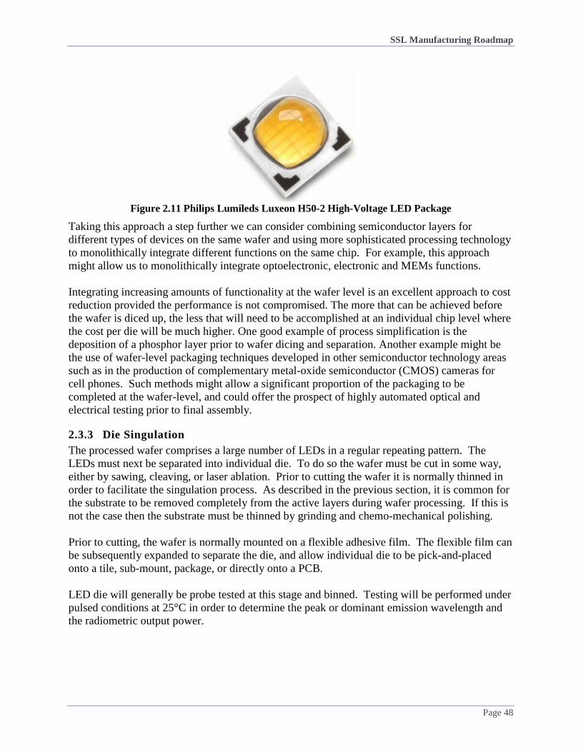
SSL Manufacturing Roadmap
Page 48
Figure 2.11 Philips Lumileds Luxeon H50-2 High-Voltage LED Package
Taking this approach a step further we can consider combining semiconductor layers for different types of devices on the same wafer and using more sophisticated processing technology to monolithically integrate different functions on the same chip. For example, this approach might allow us to monolithically integrate optoelectronic, electronic and MEMs functions. Integrating increasing amounts of functionality at the wafer level is an excellent approach to cost reduction provided the performance is not compromised. The more that can be achieved before the wafer is diced up, the less that will need to be accomplished at an individual chip level where the cost per die will be much higher. One good example of process simplification is the deposition of a phosphor layer prior to wafer dicing and separation. Another example might be the use of wafer-level packaging techniques developed in other semiconductor technology areas such as in the production of complementary metal-oxide semiconductor (CMOS) cameras for cell phones. Such methods might allow a significant proportion of the packaging to be completed at the wafer-level, and could offer the prospect of highly automated optical and electrical testing prior to final assembly.
2.3.3 Die Singulation The processed wafer comprises a large number of LEDs in a regular repeating pattern. The LEDs must next be separated into individual die. To do so the wafer must be cut in some way, either by sawing, cleaving, or laser ablation. Prior to cutting the wafer it is normally thinned in order to facilitate the singulation process. As described in the previous section, it is common for the substrate to be removed completely from the active layers during wafer processing. If this is not the case then the substrate must be thinned by grinding and chemo-mechanical polishing. Prior to cutting, the wafer is normally mounted on a flexible adhesive film. The flexible film can be subsequently expanded to separate the die, and allow individual die to be pick-and-placed onto a tile, sub-mount, package, or directly onto a PCB. LED die will generally be probe tested at this stage and binned. Testing will be performed under pulsed conditions at 25°C in order to determine the peak or dominant emission wavelength and the radiometric output power.
SSL Manufacturing Roadmap
Page 49
2.4 LED Package Manufacturing The LED package remains a key component within the LED-based luminaire and represents a significant cost element. Efforts to reduce costs while continuing to improve performance will require concerted action throughout the manufacturing supply chain. Such efforts will focus on higher quality and lower cost raw materials, improved epitaxial growth equipment and processes, optimized wafer processing equipment, and more efficient packaging methods and equipment. Various raw materials feed into the manufacturing process such as substrates, phosphors, gases, and chemicals (described in Section 2.2). The same companies listed in Section 2.3 that manufacture LED die also manufacture LED packages although it should be noted that these operations are mostly carried out in Asia. In general they will make use of their own die but on occasion they will use die from other manufacturers. Beyond these tier 1 manufacturers there are a number of companies that rely entirely on other manufacturers for their die. These include GE Lighting in North America, and Lextar, Lite-On, and Unity Opto in Asia. An outline of the LED package manufacturing process is provided in the following sections.
2.4.1 Die Packaging Die packaging is heavily based on equipment and processes developed for the general semiconductor die packaging industry. Certain customization has been required but to a large extent existing equipment is already suitable. There is a high degree of commonality with regard to packaging materials such as ceramic packages and sub-mounts, and surface mount technology. Similarly, the industry has been able to employ many of the existing processes and equipment for die-attach, wire bonding, flip-chip, encapsulation, and lens attach. Probably the most critical difference occurs in the controlled application of a phosphor or other down-conversion material to the die to create a phosphor-converted white LED. There are a multitude of options regarding the packaging of LED die in terms of the package design and packaging materials employed. Ultimately the packaging method reflects the target application, and the end result is a wide range of different types of package in terms of physical dimensions and light output characteristics. Traditionally the focus has been on the manufacture of high power 1 W packages comprising a single 1 mm2 die and producing around 80-100 lumens of white light. Such packages use relatively expensive ceramic materials on account of their superior thermal properties. A more recent trend has been to utilize lower power LED packages originally developed for the backlighting industry. Such products use inexpensive plastic packaging materials resulting in very low cost packages, and while the lumen output per package is much lower it is possible to use many more packages to achieve similar overall light output levels in a cost effective manner. Low cost plastic packages are well suited to the manufacturing of diffuse lighting sources, while compact high power packages are well suited to the manufacturing of high intensity point sources. In this context it has been common to refer to medium power and high power packages to distinguish between plastic packages with power dissipations of around 0.5 W or less, and ceramic packages with power dissipations over 0.5 W. Although the recent introduction of 1 W products based on plastic quad flat no-lead (QFN) packages by companies such as Nichia (757 series) and Toshiba (TL1F1 series) are blurring these lines.

SSL Manufacturing Roadmap
Page 50
In common with die manufacturing process, there has been a growing trend in LED package manufacturing toward modularization to cope with the ever widening portfolio of package designs. One approach being employed by Philips Lumileds is to identify a small number of basic building blocks which can be combined in many different ways to produce a range of different package products, from compact single die packages to large CoB packages. This approach is illustrated in Figure 2.12.
Figure 2.12 Example of Modularization in LED Package Manufacturing
Source: Iain Black, Philips Lumileds, SSL Manufacturing Workshop, Boston, MA, June 2013 The Luxeon Z package shown in Figure 2.13 epitomizes the design of a simple compact building block. The Luxeon Z is an ultra-compact (1.3 mm x 1.7 mm), surface mount package for a high-power monochromatic color LED or a white LED. The package area is only slightly larger than the die area (1 mm x 1 mm). Each Luxeon Z emitter consists of a high brightness InGaN or AlInGaP LED die on a ceramic substrate. A yellow colored phosphor layer is deposited over a blue die for the white emitting version. The ceramic substrate provides mechanical support and a thermal path from the LED chip to the bottom of the package. An interconnect layer electrically connects the LED chip to cathode and anode pads of equal size on the bottom of the ceramic substrate. The undomed device architecture provides additional design flexibility.
Figure 2.13 Luxeon Z Package: (a) top view (monochromatic emitter), (b) rear view, and (c) top
view (white emitter)

SSL Manufacturing Roadmap
Page 51
The die packaging cost remains a major component of the cost of a packaged LED. The main challenge is therefore to reduce packaging costs. This might be achieved by getting more light out per package or more efficient use of raw materials (either using less material or finding more affordable alternatives) to enable the manufacturing of lower cost LED packages without compromising on performance. Using advanced silicone and thermal packaging materials enables higher current and higher temperature operation enabling more light output, effectively reducing the cost or package (per lumen). The recent move to lower power operation and plastic packages for lighting class LEDs provides a major cost saving. Such packages use smaller, and therefore cheaper, die and since they operate at low powers, they don’t require expensive thermal solutions such as the use of ceramic materials and metal clad printed circuit boards (MCPCBs). Multi-die packages are commonplace with many identical die configured in regular arrays. Such packages provide large lumen outputs. Future developments in packaging technology are likely to involve the integration of different types of die to create new functionality. One example is the integration of an AlGaInP-based red/amber LED die with a white LED die to achieve higher efficacy and improved color quality [27]. Another example might involve the integration of multiple monochromatic LEDs to achieve a white light source with high efficacy, high CRI, and tunability over a wide range of color temperatures. Electronic components might also be integrated with the LED die such as the driver IC, or sensors and control ICs.
2.4.2 Down-converter Application The application of phosphors or other down-converter materials to achieve high quality white light of the specified color quality and color point requires careful control of material composition and layer thickness. As the color coordinate tolerance is tightened it is often necessary to employ a tunable phosphor application process where each die is tested prior to phosphor application to achieve the target color point. The availability of more uniform and reproducible phosphor materials would help eliminate such matching processes and reduce costs. There are many different methods to apply the phosphor to the die ranging from the relatively simple “dam & fill” method, through conformal methods such as electrophoretic deposition or the use of phosphor loaded ceramic discs (e.g., Lumiramic), to remote methods. Different package types suit different application methods with the simpler and cheaper “dam & fill” being largely confined to medium power LEDs using plastic packages and chip on board packages while the more expensive conformal methods used for high power LEDs using ceramic packages. A good example of phosphor applied at the package level is shown in Figure 2.13 where the Luxeon Z package is shown as a blue monochromatic light source and after a phosphor layer has been deposited over the entire top surface to create a white emitting light source. Remote phosphors are generally applied as a coating to optical elements positioned above and around the semiconductor die (e.g., the Vio® product manufactured by GE Lighting uses a remote phosphor dome in conjunction with a violet LED). Further improvements in application flexibility to meet the wide range of demands for current and new package designs is required along with suitable equipment to meet that demand.
2.4.3 Encapsulation and Lensing The LED die is encapsulated to provide environmental protection. Encapsulation is generally accomplished through the application of a silicone-based dielectric layer. Only certain grades of

SSL Manufacturing Roadmap
Page 52
silicone material are suitable for this application since they must be stable with respect to the elevated operating temperatures and a high optical flux density. Sometimes the same silicone material is molded to form a lens over the LED. Alternatively a separate lens can be attached above the encapsulation layer. The lens assists with the efficient extraction of light from the LED and controls the emission characteristics. As described in the previous section, it is common for the silicone material to provide a matrix for the phosphor or down-converter material. In this case the phosphor/down-converter material is dispersed within the silicone matrix prior to being deposited over the LED die.
2.5 LED Luminaire Manufacturing Manufacturing of an LED luminaire involves combining the LEDs with mechanical and thermal components such as the heat sink, optical components to tailor the light distribution, and LED drive electronics. The various sub-systems are discussed separately below before considering the complete luminaire.
2.5.1 LED Die and Packages in Luminaires LED die or packages are a critical component of all LED-based luminaires, and luminaire manufacturing is profoundly affected by LED package cost, performance, color consistency, form factor, and availability. Since the beginning of the DOE SSL Manufacturing R&D effort, Workshop participants have consistently proposed that the DOE support R&D in the areas of current droop and IQE as a means of reducing the relative cost contribution of LED packages within the luminaire. Improved LED efficiency and reduced droop will not necessarily reduce the cost of LED components (and may make them more expensive) but would reduce the number of expensive LED components required in a luminaire design and reduce the amount of thermal handling for a given lumen output. In addition, consistent, efficient, and stable emitters are desired across the visible spectrum. These LED R&D topic areas are appropriate for the Core Technology Research or Product Development activities and are discussed in the 2013 MYPP. While advances in LED component performance continue to be made, luminaire manufacturers must, make do with the LED packages that are currently available. From a manufacturing R&D perspective there are alternative strategies that can be employed to reduce luminaire cost. A key metric to be optimized is the lumen output per dollar (lm/$) and improvements can be achieved in two distinct ways. One approach mentioned above is to drive a high power LED package at higher currents in order to achieve higher lumen output. Fewer LED packages will be required but the lumen output gains will be at the expense of efficacy. Nevertheless, continuous improvements in package efficacy have made this approach practical. An alternative approach gaining traction in the industry is to utilize lower cost plastic packages originally designed for the display backlighting industry. Such packages are much cheaper so they can be used in large numbers to achieve a specific lumen output while retaining a high lm/$, and recent improvements in efficacy and color quality control has made this a viable option for high performance luminaires. This latter approach is particularly attractive for distributed lighting sources such as tube replacements or omnidirectional lamps. Significant progress has also been made in terms of reducing performance variability for LED packages. Binning of LED packages in terms of lumen output, CCT, and forward voltage, is still

SSL Manufacturing Roadmap
Page 53
routinely performed by the manufacturer but increasingly this testing is performed at temperatures closer to the luminaire operating temperature (85°C) and most product is guaranteed to fall within 4 to 5 SDCM, with certain products available in 1 to 2 SDCM bins at a premium price. Manufacturers are therefore able to select product that closely meets their performance requirements although costs will increase as the specification is narrowed. In order to achieve tighter tolerances while maintaining competitive prices, some manufacturers have developed sophisticated mixing approaches to make use of lower cost products falling further from the black-body locus. Regarding color consistency, there is an ongoing need for research into the sensitivity of the market for color variation – what is humanly visible and what is the tolerance for variations in color and output with respect to the lighting application? This aspect is discussed further in the 2013 MYPP.4 Color and output shift with time and temperature for different color LEDs must also be dealt with in the product design and manufacturing processes. A common scheme involves mixing a white LED with a red/amber LED but more complex schemes using larger mixtures of colors can be considered. Such luminaires may require the integration of optical sensors and control systems, although simpler control systems have been successfully developed using control algorithms for the white/red mixing scheme.
2.5.2 Remote Phosphors Phosphor or down-converter material is normally applied at the package level however it can also be applied at the luminaire level. Phosphor conversion at the luminaire level is achieved by the use of a phosphor coated optical material placed some distance above blue emitting LEDs. This method is referred to as a remote phosphor. The main advantage of a remote phosphor is that the whole surface of the shaped optics uniformly emits white light, giving an omnidirectional diffuse light output. Another advantage is that the blue emission from the pump LEDs can be averaged to provide a consistent color point. The main disadvantages are that much larger volumes of phosphor material must be used and deposition uniformity must be maintained over larger areas. A good example of a lamp using the remote phosphor approach is the Philips A19 L•Prize bulb shown in Figure 2.14.
4 The 2013 SSL MYPP is available at: http://apps1.eere.energy.gov/buildings/publications/pdfs/ssl/ssl_mypp2013_web.pdf

SSL Manufacturing Roadmap
Page 54
Figure 2.14 Philips A19 L•Prize Bulb Source: http://www.usa.philips.com
Companies such as Intematix in North America are able to supply sheets, or custom molded shapes, of remote phosphor material (ChromaLitTM) with well-defined performance characteristics when combined with blue LEDs.
2.5.3 Optical Component Manufacturing Luminaires incorporate a variety of optical elements to optimize light extraction and tailor the light distribution. These elements might be refractive, reflective or diffusive in nature depending on the application. Manufacturers of optical components include CARCLO, LEDiL, Khatod, WhiteOptics, and Luminit.
2.5.4 LED Driver Manufacturing Drivers remain a critical component in all LED-based luminaires and can significantly impact luminaire performance and reliability. They are most often cited as the cause of failure for luminaires. Features built into the driver such as controls can add value to LED lighting products. Most of the issues associated with drivers remain the same as discussed in previous revisions of this report. These issues are more related to product performance and cost trade-offs than they are to manufacturing technology. The manufacturing of drivers is well understood and can be done at low cost if the product performance requirements are well understood. While basic driver manufacturing technology may be well understood, the need for drivers with improved integration, reliability, and flexibility within the luminaire remains. Approaches for the development of flexible, high efficiency, low cost drivers could include the disaggregation of driver functionality into sub-modules to allow luminaire integrators to mix and match functions while maintaining high efficiency and reliability. The manufacturing of drivers with some level of controllability and control compatibility is also a concern for driver and luminaire

SSL Manufacturing Roadmap
Page 55
Proposed driver information:
• Operating temperature range; • Efficiency with respect to power,
load, and temperature; • Input voltage and output voltage
variation; • Off-state power; • Power to light time; • Power overshoot; • Transient and overvoltage
protection specifications; • Compatibility with specific
dimming protocols; • Compatibility with ambient light
sensors; • Harmonic distortion in power
supply; • Output current variation with
temperature, voltage, etc.; • Maximum output power; • Power factor correction.
manufacturers. Luminaires for varying lighting applications may require different types of control. Internal electronic control of color consistency, compatibility with multiple dimming systems, or communication with various forms of wired or wireless controls may be required for the lighting application and this functionality is typically integrated into the power supply. The need for the integration of these controls into the luminaire can impact the assembly costs of the luminaire as well as the reliability of the luminaire. Improvements to the design and manufacturing of drivers and the control systems could have a significant benefit on luminaire cost, performance, and reliability. Previous calls have been made for a standard report format of driver performance to facilitate driver integration into LED-based luminaires. The lack of information and inconsistent reporting of driver performance was thought to be inhibiting efficient and easy integration of the electronic components. It was also felt that a standard reporting format would facilitate the use and development of analysis, simulation, and design tools for luminaire manufacturers. The sidebar lists a number of parameters that should be included in such a report. Nevertheless, despite these calls, there has not been any significant movement on this issue. There is also a need to develop a testing protocol to better define driver performance and reliability. In this case some progress has been made. For example, an ANSI lighting group committee is currently working on an LED driver testing method (ANSI C82.XX) and a driver performance standard (ANSI C82-SSL1-20XX). Also, the DOE SSL Program is supporting product development R&D to better understand and predict driver reliability. Manufacturers of complete driver sub-assemblies include the vertically integrated luminaire manufacturers and specialist driver manufacturers such as iWatt in North America, and Meanwell in Taiwan. Luminaire manufacturers have recently been acquiring these specialist driver manufacturers. For example, GE Lighting acquired Lightech in July 2011 and Acuity Brands acquired eldoLED in March 2013. LED driver IC manufacturers include (listed alphabetically) Allegro Microsystems, AnalogicTech, Analog Devices, Austriamicrosystems (AMS), Cirrus Logic, Diodes, Inc., Exar, Fairchild Semiconductor, Freescale Semiconductor, Infineon Technologies, Intersil, iWatt, Leadis Technology, Linear Technology Corp., Macroblock, Marvell, Maxim Integrated Products, Monolithic Power Systems, National Semiconductor (now part of Texas Instruments), NXP Semiconductors, ON Semiconductor, O2 Micro, Power Analog Microelectronics, Power Integrations, Richtek, Rohm Electronics, Semtech, Silicon Touch Technology, Skyworks, STMicroelectronics, Supertex, Texas Instruments, and Toshiba.

SSL Manufacturing Roadmap
Page 56
According to MarketsandMarkets, Inc., the Asia-Pacific region dominates the LED driver IC market, capturing a 59.6% share of the close to $1 billion market [28]. This is mainly due to the low manufacturing cost, presence of original equipment manufacturers/original device manufacturers (OEMs/ODMs), and favorable government tax exemptions. In 2010, display back-lighting accounted for around 80% of the market but will decrease to around 66% by 2015 due to the more rapid growth being experienced by the lighting segment (46.5% CAGR).
2.5.5 Luminaire Manufacturing The term ‘luminaire’ is used to describe fully integrated luminaires as well as LED-based replacements lamps, which have the same level of integration but a standard electrical interface for use within conventional lighting fixtures. Manufacturing of LED-based lighting products share little in common with conventional lighting products since conventional lighting technologies tend to be based around the fixture-plus-bulb paradigm with the manufacturing of each part handled completely separately and by separate companies. The integrated nature of an LED-based lighting product serves to combines the fixture, light engine, and driver electronics in a single unit, which significantly complicates the manufacturing process. However, as the LED manufacturing components and processes become more mature, and manufacturers gain experience, the LED luminaire manufacturing process may no longer be considered quite so ‘complicated’ and much of the uncertainty (and cost) will be removed from the process. Discussions regarding simplification of the manufacturing process include the following themes:
• Reducing interfaces- One method to simplify the manufacturing process is to streamline the integration of the luminaire by simplifying interfaces between the sub-components of the luminaire. Two divergent approaches have been proposed for simplifying interfacing between luminaire components. Within the LED luminaire products there are opportunities to better integrate the LED die, LED package, or LED module with the lamp mechanical, electrical, and optical structures. Such advancements could simplify the design of the lamp or luminaire products, simplify the manufacturing of these products, and reduce product costs. The potential for high levels of component integration within LED-based luminaire products will have a significant impact on how such products will be manufactured. This level of integration may require automated manufacturing to bring down the assembly costs and reduce human variations in the manufacturing process. This integration also represents a challenge for existing luminaire manufacturers who may not have the necessary tools or expertise to develop the LED-based products. For example, the LED chip could be mounted directly to the luminaire heat-sink removing several layers of material and thermal interfaces, if an appropriate manufacturing method could be developed. This would remove the distinction between the LED package or light module and the luminaire. This is just one example, but the thermal, mechanical, optical, and electrical interfaces could all be considered for enhanced integration. Novel materials could also be considered which could simplify manufacturing and reduce the complexity, cost, and weight of the luminaire. Luminaire manufacturing would benefit from lighter weight and lower cost heat-sinks and thermal handling materials. Luminaire and LED modules could also benefit from lower cost but similarly robust optical materials.

SSL Manufacturing Roadmap
Page 57
• Modularization- A second approach would be to develop a modular approach to luminaire manufacture. This would be achieved by developing standardized form factors and interfaces between sub-components, which would allow for a consistent integration process regardless of the supplier of the sub-component. This approach is being considered and supported by an industry consortium – the Zhaga Consortium. The components of the luminaire, such as the LED light engine, driver, thermal handling, and optics, and housing, could be developed to readily fit together in a variety of configurations. This could enable rapid manufacturing of a range of product variations, simplify inventory demands, and simplify luminaire design. All of these benefits could lead to greatly reduced luminaire costs. The modular manufacturing and design approach could also benefit smaller scale and traditional luminaire manufacturers who could more easily and rapidly design and manufacture LED-based lighting products. Different lighting applications and types of products may lend themselves to either integrated or more modular product designs. In addition, different levels of design capability for luminaire manufacturers may also encourage the use of more modular product designs. While the modular approach simplifies integration and supply chains, there are inevitable performance limitations as the general-purpose modules cannot be optimized for each specific lighting application. Multiple approaches to the design and manufacturing of LED-based lighting products will likely exist in parallel as the market evolves.
• Efficient testing-
A third method to simplify the manufacturing process is to simplify luminaire testing requirements. It has been suggested that this could be partially achieved by changes to testing policies and standards. In terms of manufacturing R&D, testing simplification could be accomplished through a more consistent supply of incoming components, particularly LED packages. Testing the luminaires at critical points in the manufacturing process and relating the test results to final luminaire performance could also simplify testing (see Section 2.6.4). Lastly, design modeling software could enable more rapid product design with a range of incoming components and anticipate product performance (see Section 2.6.2). In-line testing and design software could also expedite the development of similar products within a product family enabling a more flexible manufacturing process. For example, common sub-components to a range of final products could be tested before the manufacturing process diverges.
Another fundamental change to luminaire manufacturing is how luminaire reliability is considered and how this impacts the design and sub-component selection of LED-based luminaires. The long life of the LED package has led to the expectation of longer-lived luminaires and replacement lamps. Maximizing product lifetime requires not just a well-integrated long life LED package, but also long lives from all of the luminaire sub-components and reliable design and integration of the product. While consumers expect longer lifetimes from LED lighting products they also insist on low priced products. Understanding the reliability

SSL Manufacturing Roadmap
Page 58
relationships between the luminaire components will allow manufacturers to make informed decisions regarding trade-offs between product cost and product reliability5. Discussions at recent Roundtable and Manufacturing R&D Workshops on improving the integration and manufacturing of LED luminaires and modules have emphasized the need to develop LED packages and luminaire designs that are readily integrated, use fewer raw materials, and are optimized for efficient manufacturing without compromising the performance of the light source. The benefits of these improvements would be products that weigh less, have improved thermal performance, are more reliable, have more consistent color, and can be manufactured more efficiently at a lower cost. A large and growing number of companies are involved in the manufacturing of LED-based luminaires and modules. Historical lamp manufacturing companies such as Philips, Osram Sylvania, GE, and Toshiba; luminaire manufacturers such as Cooper Lighting (now Eaton), Acuity Brands, Hubbell Lighting, and Zumtobel; and many new entrants to the lighting industry including Cree, Lighting Science Group, LG, and Samsung have all begun manufacturing LED-based lighting products.
2.5.6 Test and Inspection Test and inspection requirements associated with luminaire manufacturing include sub-assembly testing, in-line inspection, and end-of-line electrical and photometric testing. Incoming sub-assemblies must be tested and inspected in order to ensure they meet specification. Often this is performed by the sub-assembly manufacturer. In-line visual inspection is employed in order to detect manufacturing problems at an early stage and allow affected parts to be re-worked or scrapped. However the most significant test and inspection activity is associated with end-of-line testing of the completed luminaire. The introduction of LED-based lighting technology has significantly complicated the lamp and luminaire manufacturing process compared to conventional lighting products. In particular, testing requirements have become much more significant due to the fact that each LED-based luminaire is a unique fixture comprising a number of sub-components. Each LED-based lighting fixture has its own distinct electrical and photometric performance characteristics and must be separately tested (absolute photometry). Conventional lighting technologies tend to be based around the fixture-plus-bulb paradigm which allows for simple and rapid photometric testing with readily anticipated results (relative photometry). It is important to realize that the impact of test and inspection on yield, cost or performance of the final product will depend on the point in the manufacturing process that the measurement is made. These critical testing points need to be identified and exploited for their benefits to the manufacturing process. Luminaire testing currently culminates in a raft of specific compliance tests to demonstrate adherence with the requirements dictated by a number of agencies including Underwriters Laboratories Inc. (UL), DesignLights Consortium (DLC), and Energy Star (see
5 The “LED Luminaire Lifetime: Recommendations for Testing and Reporting” document can be found at:
http://apps1.eere.energy.gov/buildings/publications/pdfs/ssl/led_luminaire-lifetime-guide_june2011.pdf

SSL Manufacturing Roadmap
Page 59
Section 4). The industry is working with these compliance bodies to understand how this testing burden might be minimized.
2.6 LED Modeling and Simulation Modeling and simulation is an important activity in the design and manufacturing of the various components and sub-systems, and of the manufacturing process itself. Modeling of the impact of manufacturing actions on LED and luminaire performance can help improve the new product design process and provide an accurate prediction of final device performance and reliability. The most important types of modeling and simulation being applied to SSL manufacturing are discussed in the following sections.
2.6.1 Cost Modeling Understanding the source of costs within the manufacturing process is critical to being able to minimize the cost of the final manufactured product. Cost modeling can be used to determine those costs and to help identify those areas which have the largest impact on final device and luminaire costs. A simple modular cost model was developed previously to describe the manufacturing of an LED package and was demonstrated at the 2012 Manufacturing Workshop. Conventional cost models are based on a COO analysis for each piece of equipment in the manufacturing process. COO is a widely used metric in the semiconductor industry6 and was originally developed for wafer fabrication tools. COO can be defined as the full cost of embedding, operating and decommissioning, in a factory environment, a system needed to accommodate a required volume. In its simplest form it is the total cost of producing a good part from a piece of equipment. The cost per part for an item of semiconductor processing equipment can be determined from a knowledge of the fixed cost (purchase, installation, etc.), variable cost (labor, materials, etc.), cost due to yield loss, throughput, composite yield, and utilization (proportion of productive time). The cost per part is obtained by dividing the full cost of the equipment and its operation by the total number of good parts produced over the commissioned lifetime of the equipment. COO can also be applied to non-process equipment such as test and inspection tools. The purpose of these tools is to identify good product from bad product and generally results in some level of scrappage. Scrap caused by the inspection method, such as destructive testing, is part of the test equipment COO (increases the yield loss). Scrap identified by the inspection method is part of process tool COO for the tool causing the scrappage. The simple modular LED COst Model (LEDCOM) analyses costs within the LED package manufacturing process [29]. The model focuses on process steps contributing more than 1% to the final LED package cost. For these process steps it performs a simple cost analysis based on the equipment employed and the yield. These costs are accumulated along with the yields to establish a final manufacturing cost/wafer or cost/die. Global parameters such as substrate type, substrate diameter, die area, and factory overheads can be fixed. Each step can be repeated as many times as necessary and can be modified in terms of the equipment used and other key process variables.
6 See SEMI standard E35: Cost of Ownership for Semiconductor Manufacturing Metrics, available at:
http://www.semi.org/en/Standards/CTR_042925
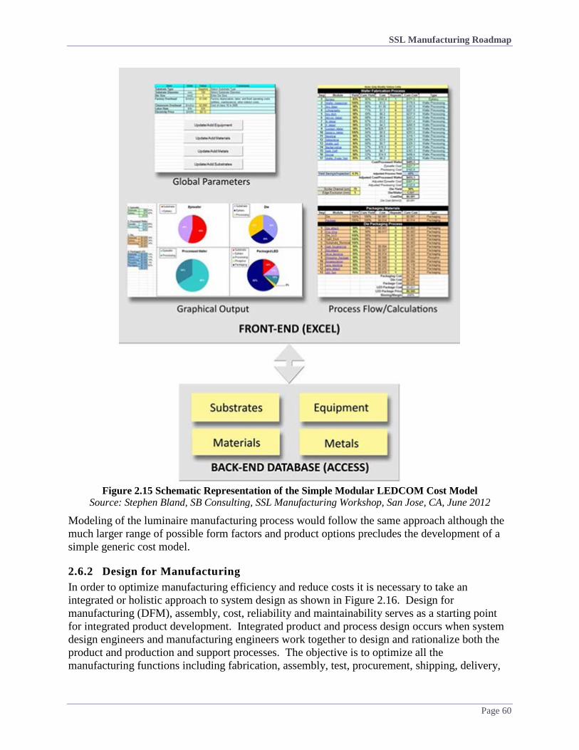
SSL Manufacturing Roadmap
Page 60
Figure 2.15 Schematic Representation of the Simple Modular LEDCOM Cost Model
Source: Stephen Bland, SB Consulting, SSL Manufacturing Workshop, San Jose, CA, June 2012
Modeling of the luminaire manufacturing process would follow the same approach although the much larger range of possible form factors and product options precludes the development of a simple generic cost model.
2.6.2 Design for Manufacturing In order to optimize manufacturing efficiency and reduce costs it is necessary to take an integrated or holistic approach to system design as shown in Figure 2.16. Design for manufacturing (DFM), assembly, cost, reliability and maintainability serves as a starting point for integrated product development. Integrated product and process design occurs when system design engineers and manufacturing engineers work together to design and rationalize both the product and production and support processes. The objective is to optimize all the manufacturing functions including fabrication, assembly, test, procurement, shipping, delivery,
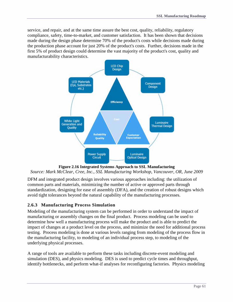
SSL Manufacturing Roadmap
Page 61
service, and repair, and at the same time assure the best cost, quality, reliability, regulatory compliance, safety, time-to-market, and customer satisfaction. It has been shown that decisions made during the design phase determine 70% of the product's costs while decisions made during the production phase account for just 20% of the product's costs. Further, decisions made in the first 5% of product design could determine the vast majority of the product's cost, quality and manufacturability characteristics.
Figure 2.16 Integrated Systems Approach to SSL Manufacturing
Source: Mark McClear, Cree, Inc., SSL Manufacturing Workshop, Vancouver, OR, June 2009 DFM and integrated product design involves various approaches including: the utilization of common parts and materials, minimizing the number of active or approved parts through standardization, designing for ease of assembly (DFA), and the creation of robust designs which avoid tight tolerances beyond the natural capability of the manufacturing processes.
2.6.3 Manufacturing Process Simulation Modeling of the manufacturing system can be performed in order to understand the impact of manufacturing or assembly changes on the final product. Process modeling can be used to determine how well a manufacturing process will make the product and is able to predict the impact of changes at a product level on the process, and minimize the need for additional process testing. Process modeling is done at various levels ranging from modeling of the process flow in the manufacturing facility, to modeling of an individual process step, to modeling of the underlying physical processes. A range of tools are available to perform these tasks including discrete-event modeling and simulation (DES), and physics modeling. DES is used to predict cycle times and throughput, identify bottlenecks, and perform what-if analyses for reconfiguring factories. Physics modeling

SSL Manufacturing Roadmap
Page 62
is used to obtain an improved understanding of the underlying physical processes using tools such as computational fluid dynamics or finite element analysis. One key element to the success of such modeling and simulation is the need to populate the models with real-time information that is collected automatically and continually. The model is refined and optimized using this information to enable it to most accurately match the observed outcomes, and ultimately to most accurately predict the impact of changes to the manufacturing process on the observed outcome. The development of suitable test and measurement equipment (see Section 2.1.5) therefore goes hand-in-hand with the development of a manufacturing process model.
2.6.4 Luminaire Reliability Modeling The lack of a thorough understanding of lifetime for LED-based luminaires continues to be a significant problem for luminaire manufacturers. While LM-79 provides a standardized protocol for measuring luminaire performance and can be performed at various points in the luminaire life, it is expensive and time consuming to perform this test, particularly at the rate new luminaire and lamps products are being developed. LM-79 also does not offer a means to accelerate life testing to allow for interpolations of lifetime within a shorter test cycle. Uncertainty in the long-term performance of the luminaire system makes it difficult to estimate and warrant the lifetime of LED-based luminaires. It also hinders manufacturers’ ability to know how best to improve their product reliability. This uncertainty could be addressed by better information about long term performance of key LED luminaire components and materials, including the LED packages, drivers, optical components and materials used in assembly, along with accepted methods to statistically predict luminaire system lifetime. These issues are discussed in more detail in Section 4.

SSL Manufacturing Roadmap
Page 63
2.7 LED Manufacturing Priority Tasks for 2013 DOE identified the following priority LED manufacturing R&D tasks based on discussions at the Manufacturing Roundtables and Workshop.
M.L1. Luminaire Manufacturing: Support for the development of flexible manufacturing of state of the art LED modules, light engines, and luminaires. Suitable development activities would likely focus on one or more of the following areas:
• Advanced LED package and die integration (e.g. COB, COF, etc.) into the luminaire, • More efficient use of components and raw materials, • Simplified thermal designs, • Weight reduction, • Optimized designs for efficient and low cost manufacturing (such as ease of
assembly), • Increased integration of mechanical, electrical and optical functions, and/or • Reduced manufacturing costs through automation, improved manufacturing tools or
product design software. The work should demonstrate increased manufacturing flexibility (processes or designs that can work for multiple products) and higher quality products with improved color consistency, lower system costs, and improved time-to-market through successful implementation of integrated systems design, supply chain management, and quality control. Metric(s) Current Status 2016 Target(s) Retail Lamp Price 50% reduction Assembly Cost ($) 50% reduction Color Control (SDCM) 7 2 – 3
In reference to M.L1, workshop participants noted that luminaire testing requirements can be burdensome to luminaire manufacturers, adding significant costs to the final product. These requirements can also delay introducing products to the market, or prohibit it altogether, especially for smaller companies with fewer resources. Participants further emphasized the importance of reducing manufacturing costs through automation, value-added luminaire technology or simple robust designs with efficient use of materials and components. Research in this area could focus on a specific portion or sub-component of the luminaire manufacturing process (while still demonstrating a full luminaire), but the work should demonstrate and describe the impact (in terms of cost or quality) within the context of the entire luminaire manufacturing process. While used as an example in the retail price metric, task M.L.1 is not limited to LED lamps. The large range of luminaires makes it difficult to generalize prices; however, all luminaires should target similar relative changes in price. The 50% reduction in retail price by 2016 is a relative cost reduction as compared to today’s market.

SSL Manufacturing Roadmap
Page 64
M.L3. Test and Inspection Equipment: Support for the development of high-speed, high-resolution, non-destructive test equipment with standardized test procedures and appropriate metrics within each stage of the value chain for semiconductor wafers, epitaxial layers, LED die, packaged LEDs, modules, luminaires, and optical components. Equipment might be used for incoming product quality assurance, in-situ process monitoring, in-line process control, or final product testing/binning. Suitable projects will develop and demonstrate effective integration of test and inspection equipment in high volume manufacturing tools or in high volume process lines, and will identify and quantify yield improvements. Metric(s) Current Status 2016 Target(s) Throughput (single bin units per hour) 2x increase Cost of Ownership 50% reduction $/Units per hour
Since device testing and specification costs translate all the way up to the luminaire, one specific area of interest, discussed at the workshop, was the interaction between device and luminaire testing, specifically if better binning and testing at the device level would circumvent some end-of-the-line luminaire testing. As a manufacturer, having a wide distribution of photometric performance can be an important cost driver. Since device testing and specification costs translate all the way up to the luminaire, one specific area of interest, discussed at the workshop, was narrowing the process window for test and inspection, specifically if in-situ test and inspection could circumvent some end-of-the-line luminaire testing.

SSL Manufacturing Roadmap
Page 65
M.L7. Phosphor Manufacturing and Application: This task supports the development of improved manufacturing and application of down-converter materials, used in solid state lighting. This could include projects focused on phosphors to increase production volume and manufacturing techniques to improve quality and reduce performance variation. This task also supports the developments of down-converter materials, application materials, and techniques which improve color consistency of the packaged LEDs and reduce the cost without degrading LED efficacy or reliability. Metric(s) Current Status 2016 Target(s) Material Usage Efficiency 50% 90% Δ u’v’ Control 0.0127 < 0.0048 Materials Cost ($/klm) 15% reduction per year (D90-D10)/D50 (Conventional Phosphor) 30 10
FWHM (Quantum Dots) 40nm < 30nm Work in this R&D area could focus on reducing process variation for existing materials or phosphor modeling efforts. Phosphor modeling would allow manufacturers to better understand and improve material consistency. The current lack of consistency between phosphor batches is significant and requires that manufacturers test all incoming materials. Participants also highlighted two specific areas of interest; collaboration to promote progress on the development of higher-level processing techniques and collaboration to reduce costs associated with this task.
7 Applies to full distribution of LEDs (not at luminaire level) 8 At fixed blue wavelength

SSL Manufacturing Roadmap
Page 66
3 OLED PANEL AND LUMINAIRE ROADMAP At present, lighting panel products that are suitable for general illumination are manufactured using vapor deposition techniques on small-scale lines. These panels are built on rigid, display grade glass using batch processes and multi-emitter stacks or tandem structures. Encapsulation is accomplished with a glass cover and light output is enhanced using external extraction films. This approach is too costly, however, and many avenues are being explored to lower cost and improve performance. Materials cost reductions and innovative solutions for low-cost equipment and processes are needed. Choosing a successful approach involves optimizing performance while considering processing and tooling issues. Some of the manufacturing strategy considerations are identified below:
• Dry (evaporation) versus wet (solution) processing- Since the performance of wet-processed emitters is still lagging, short term interest is in the use of coating processes for the anode structures, hole injection layer (HIL) and hole transport layer (HTL). This offers significant cost savings through the elimination of the lithography steps and subsequent higher utilization of the conducting materials. The techniques under evaluation include ink-jet and nozzle printing, screen printing, slot-die coating and gravure printing. Although prototype panels have been produced by wet processing, no commercial production is underway.
• Substrate selection- Currently, glass is still the most convenient substrate to use in the development of manufacturing processes. Though costly display grade glass is the standard choice, low-cost float glass substrates may offer a short term solution for immediate cost reductions. The adoption of plastic is being retarded by the unavailability of cost-effective and reliable manufacturing techniques for defect-free barrier layers. Rapid atomic layer deposition is being explored as an alternative to standard deposition processes for the inorganic layers in multi-layer barriers, but its commercial viability has not yet been established. The use of metal foils as substrates or covers has been confined to research laboratories.
• Roll-to-Roll versus Batch Processing- Currently, panels are produced using batch processes and this is the preferred approach for the near term. It has been argued that R2R manufacturing simplifies substrate handling and so can increase total throughput. Experiments in Taiwan and Europe using both vapor deposition and solution processing have shown that this approach is feasible, but there has been no demonstration that this approach offers substantial cost benefits in comparison with in-line batch systems. One of the problems is that R2R operation requires relatively large scale production and thus large amounts of material, even at the R&D stage. It can thus be particularly expensive to produce panels while yields are low. R2R still remains as an attractive long-term option for the production of flexible panels. However, in the short-term it seems more likely that flexible panels will be fabricated on

SSL Manufacturing Roadmap
Page 67
a rigid substrate and then lifted off. Once the manufacturing processes have been optimized and yields improved, transition to R2R production will be more affordable.
• Complexity level-
Reduction in the number of organic layers could lead to lower capital costs and higher yields. Most plans to accomplish this involve solution processing, but it has not yet been shown that the DOE performance targets can be met using this approach.
• Throughput scaling-
Most OLED proponents argue that substantial cost reductions can be achieved only through increased throughput from each line. Scaling in size will require substantial added capital investment. Cycle times well below 60 seconds are desired, but little progress has yet been reported. Others argue that uncertainties in the market size favor the development of less expensive equipment and better material utilization with modest throughput. The feasibility of this approach may become clearer in the next year through the experience of OLEDWorks.
The OLED community has not yet settled on a set of materials or a manufacturing approach for cost effective lighting panels. At the Manufacturing R&D Roundtable it was noted that around 15 major concepts are being pursued and that over 200 materials are available for incorporation in the organic stack. Choosing a successful approach involves optimizing performance while considering processing and tooling issues. Increased collaboration among manufacturers is needed to narrow down the options and to enable high-volume manufacturing to be undertaken with confidence. Some of the specific issues that concern equipment and materials are discussed in Sections 3.1 and 3.2, prior to discussion of the manufacturing processes for panels in Section 3.3 and luminaires in Section 3.4.
3.1 OLED Manufacturing Equipment As described in Section 3.3, the traditional approach to manufacturing OLED panels has been to form all the internal layers onto rigid substrates using vapor deposition under high vacuum conditions. These techniques are discussed in Section 3.1.1, while alternative approaches using solution processing and roll-to-roll handling are outlined in Sections 3.1.2 and 3.1.3. The final critical step is encapsulation, as described in Section 3.1.4. The capital cost of the equipment used for manufacturing OLED lighting panels is very high. The amount is strongly dependent on the size of substrate used. While pricing is uncertain as high volume lines are not yet in use, the costs can be estimated as shown:
• $50-100 million for “Gen 2” at size 370 x 470 mm (0.17 m2), • $150-300 million for “Gen 5” at size 1100 x 1300 mm (1.4 m2), • $300-600 million for “Gen 8” at size 2200 x 2500 mm (5.5 m2).
With traditional manufacturing techniques, approximately half of the capital cost is associated with deposition of the organic layers and the cathode. The cost of patterning equipment for integrated substrates is substantial, but this investment can be borne by the substrate supplier, rather than the panel maker.

SSL Manufacturing Roadmap
Page 68
Part of the reason for the high cost is that the structure of high-performance OLED lighting panels is relatively complex:
• Double or triple stacks help to lower the current density and increase operating lifetimes. • Separate layers for red, green and blue emitters lead to higher efficacy and stability. • Adding metal grids to transparent electrodes improves the uniformity and reduces ohmic
loss. • Extraction enhancement layers are needed to minimize light trapping inside the panel. • Very effective barriers must be deployed to prevent ingress of water and oxygen.
The linear production lines constructed by LG Chem and First O-Lite employ around 20 deposition chambers, each of which can cost over $1 million at Gen 2 size. Reducing the number of organic layers should lead to reduced capital costs, but more effective light extraction structures would be needed to compensate for lower efficacy of the emitters.
3.1.1 Vacuum Processing Equipment Equipment costs are a major component of the total OLED cost of manufacture. The cost of ownership needs to be reduced by lowering capital costs and increasing the throughput and yield. Some equipment can be eliminated through OLED design simplification and advancements. For vacuum processing equipment cost reductions, innovations are needed in the following areas:
• Patterning for wire grid formation, • Simplification of device architecture, • Cost effective, small scale production facilities, and; • Reduced cycle times.
Sputtering has been the preferred technique for the first electrode, while the organics and second electrode are usually deposited by evaporation. Each of these techniques leads to a layer of material across the whole workpiece. Some degree of patterning is needed in lighting applications, although this does not have to be accomplished with the fine resolution needed in displays. Photo-lithography has been used to pattern the anode structure, with its sheet of transparent conductor (TC) supplemented by a wire grid. This is time-consuming and expensive. Alternative ways to remove unwanted TC materials from around the edge of each panel include laser ablation and such equipment is readily available. Another approach is to use a relatively crude mask to define the area within which the TC materials are needed. Neither of these solutions is optimal for forming the grids, since metal is needed over a small fraction of the total area. Techniques that do not rely on subtraction patterning, such as stamping or printing could help eliminate unnecessary expense. LG Chem and other companies have often stated that the most straightforward way to reduce the cost of vacuum deposition is to move to larger substrates, such as Gen 5 or Gen 8. One reason is that the production capacity scales more rapidly than the anticipated cost. Another is that the material utilization improves, since the ratio of useful substrate area to unproductive edge area increases. Appropriate equipment from companies such as Aixtron, Applied Materials and Sunic Systems has been tested in Korea and in Europe. However, it will be many years before the

SSL Manufacturing Roadmap
Page 69
market is developed sufficiently to justify the high levels of production that would come from even a single line of these sizes. This has led some manufacturers, such as Trovato, Manufacturing to prioritize introducing innovations that can lead to manufacturing cost reductions without scaling up the production process. Reducing the cycle time is one route to lower cost of ownership for manufacturing tools. The traditional cycle time for display manufacturing is approximately 90 seconds, whereas that of most existing lighting lines is longer. The commercial success of OLED lighting could be enhanced significantly if the cycle time could be reduced to below 60 seconds. This drove Moser Baer to explore small-substrate techniques similar to those used in the optical disk industry. Although there is no evidence yet that high performance OLED panels can be manufactured in such short times, this approach is being pursued by several manufacturers. One problem in accomplishing this with the standard evaporation technique is that rapid deposition requires high evaporation temperatures. Intricate molecules become fragile at high temperatures and so the challenge is to find materials that are exceptionally stable or to restrict the time the source gases remain at high temperatures. The deposition rate also influences the film structure and surface morphology with lower deposition rates typically producing smoother, higher quality films. The typical layer thickness for organic emitters is 10-30 nm. Thus deposition rates of around 1 nm/s are needed to achieve the desired cycle times. However, the transport layers are often much thicker to reduce losses through plasmon excitation at a metal electrode and to guard against shorting at transparent electrode structures. Thus faster deposition of these layers may be needed. It is possible that transport materials may be more tolerant of high temperatures than the more intricate emitters. However, many developers have suggested that the use of wet deposition techniques, such as slot-die coating may be more appropriate for some of the transport layers. The challenge then is to minimize the drying time. A second challenge is to reduce the time lost in moving the substrate from one tool to the next. This has been part of the rationale for the use of R2R equipment. However, the development of R2R tools appropriate for high-performance organic materials (and the materials themselves) has been slow and they do not appear to be ready for commercial deployment as discussed in Section 3.1.3. The alternative is to use sheet processing with a linear configuration in which the substrates can move smoothly from each stage to the next. The fact that accurate registration is not needed in lighting applications makes this approach more feasible than for high-resolution displays. An alternative approach being proposed by equipment manufacturers for stationary substrates is to use deposition tools with multiple sources so that several layers can be added in a single stage. A good example of the status of organic deposition equipment for lighting is provided by the pilot line sponsored by the Ministry of Knowledge Economy in Korea [30]. The substrates move steadily through 1000 x 1200 mm deposition chambers at a speed of 1.4 m/min, consistent with a 60s cycle time. A 50nm layer of a relatively simple organic material (Alq3) was deposited from a linear source at a rate of 2 nm/s with high uniformity (+1.3%). However, it is not clear whether such good performance could be obtained with the more delicate materials that achieve higher luminous efficacy.

SSL Manufacturing Roadmap
Page 70
3.1.2 Solution Processing Equipment Though vapor deposition is the current and most promising near term approach, development of solution deposition techniques and materials is underway. In the long term, as performance improves, these methods may allow for substantial cost reductions as materials utilization can be much more efficient using solution deposition techniques. Many prototype panels are being produced that feature one or more solution processed layers. These hybrid devices are the next step towards completely wet processed devices. The viability of using solution deposition for the emitting layers has been demonstrated by companies developing these materials, such as Sumitomo Chemical, Mitsubishi/Pioneer, and Konica Minolta. Rapid deposition of both organic and inorganic materials can be accomplished by forming inks in which the desired material is trapped temporarily in a solvent. The inks can then be applied to the substrate by jetting or by contact printing. The solvent is then removed through a drying process. Two versions of jetting have been explored with organic materials and metals. The use of 2-D patterns can be formed through ink-jet printing (IJP), in which the ink forms droplets as it leaves the printer. This method is often used in making OLED displays with 2D array of small pixels. In nozzle jet printing, the ink flows continually and stripes can be formed more uniformly. The application of ink-jet printing for depositing OLED materials was pioneered by Epson and CDT/Sumimoto, but tools are now available from several suppliers, such as Fujifilm Diamatix. Sumitomo have set a target date of 2015 for the commercial introduction of lighting panels, based upon ink-jet printing of their polymer-based materials. Nozzle printing equipment has been adapted by Dai Nippon for OLED materials from DuPont. This technique was used by DuPont Displays to develop color tunable and illuminance variable OLED panels in a project supported by the DOE SSL Program. Figure 3.1 shows a prototype desk lamp designed in conjunction with Litecontrol that features these panels. Although Samsung has been testing the nozzle printing approach, no schedule has been announced for adoption in commercial products.
Figure 3.1 Desk Lamp with Color Tunable and Illuminance Variable OLED Panels – Solution
Processed using Nozzle Printing Equipment Designed by DuPont Displays and Litecontrol

SSL Manufacturing Roadmap
Page 71
Contact printing methods that have been used for OLEDs include slot-die coating, screen printing and gravure printing. Although slot die coating has traditionally been used to create a uniform layer across the whole substrate, it has been recently demonstrated that multiple panels can be formed, with no deposition between the individual panels, as shown in Figure 3.2.
Figure 3.2 Slot Coater Adapted for Coarse Patterning Source: Robbie Charters, nTact, 2012 Flexible Electronics & Displays Conference & Exhibition, Phoenix
The quality of the film can be optimized by varying the thickness of the slot and the size of the gap between the slot and the substrate. Throughput is governed by the rate at which the substrate moves past the slot. Speeds of 100 mm/s and higher have been demonstrated for both organic materials and inks containing silver nanowires. Tools that are specially designed for this application are available from suppliers such as mBraun, nTact and Tazmo. Since even relatively thick coatings can now be deposited rapidly, the rate-limiting step is often the solvent drying process. Although some experiments have been carried out with UV-curable materials, thermal drying is still the preferred approach. Several minutes may be required to remove all of the solvent. With sheet-to-sheet handling, the process times can be matched by using long ovens or by stacking substrates. In R2R systems, the web can be looped between several rollers within the oven.
3.1.3 Roll-to-Roll Processing Equipment R2R processing could be a potential avenue for low cost production, but it is still a long way off from implementation. Konica Minolta and Sumitomo Chemical have recently reasserted their view that R2R processing will provide an economic route towards the manufacture of OLED lighting panels. Konica Minolta prefers to use slot-die coating to deposit the small molecule, solution processed organic layers. Although they demonstrated panels with efficacy of 52 lm/W using a simple four layer structure back in 2010 (in collaboration with GE), improved performance has not yet been reported and Konica Minolta is producing their current Symfos panels by vapor deposition onto rigid sheets using the Philips line in Aachen. However, the viability of the R2R approach seems to depend on the simplification that could result from the design of high-performance panels with fewer layers. This has been the traditional approach with polymer molecules, but the performance of these materials still lags that of small molecules deposited in vacuum. This provides incentive to develop simple structures for solution-processed small molecules, such as that suggested by Hitachi [31].
Coating Direction
Coating Die
Selective Coating Tray
Bare Substrateb

SSL Manufacturing Roadmap
Page 72
A major obstacle to implementation of roll-to-roll processing on plastic substrates has been the unavailability of effective barrier films to prevent ingress of oxygen and water. Although there have been many laboratory demonstration of such films, the production of defect-free films in high volume at affordable costs has not yet been achieved. A possible alternative route is through the use of ultra-thin glass. Rolls of glass with thickness down to roughly 50 µm are now available from several vendors. In November 2012, the Industrial Technical Research Institute in Taiwan announce that they had completed a full R2R processing line using 100 µm glass from Corning and had applied the line successfully to the manufacture of touch panels. OLED lighting is one of the intended applications for this technology. R2R web handling is compatible with both vapor deposition and solution processing. Gateways have been available for several years to allow the web to flow between tools at widely different pressure and have been used successfully in OLED fabrication at both the Fraunhofer Institute (COMEDD) and GE Lighting.
3.1.4 Encapsulation Equipment The encapsulation process to form edge seals in OLEDs with a rigid substrate and cover consists basically of three steps:
• Surface cleaning, • Dispensing of the epoxy seal or frit, and; • Curing of the sealant material.
Although the surface of the substrate is often cleaned thoroughly before processing begins, additional steps may be needed to remove material that has been deposited near the edge during the formation of the OLED. Laser ablation is commonly used, but care must be taken to ensure that the debris is not trapped in the panel during encapsulation. Although assuring the integrity of the seal is extremely challenging in terms of the selection of materials, the dispensing and curing steps seem similar to those required for other electronic applications. UV curing is commonly used with epoxy materials and laser sealing with glass frit. For the early production of OLEDs, encapsulation systems were developed as part of complete fabrication systems by the Japanese companies such as Canon Tokki and Ulvac. More recently, several Korean suppliers have emerged as preferred suppliers to LG and Samsung, including AP Systems, Avaco, Jusung and LTS. Versatile systems for R&D work and small scale manufacturing equipment are available from European and North American suppliers, such as mBraun, Ossila and Nordson-Asymtek. The development of effective thin-film encapsulation could reduce the thickness and weight of glass based OLEDs as well as enabling the production of flexible panels. Equipment to form multi-layer coatings with alternating inorganic and organic layers was available from Vitex before their acquisition by Samsung. Research to provide more reliable ways to form the inorganic layers that are prone to pin-holes, cracks and other defects is underway at several companies. For example, Beneq has promoted the use of atomic layer deposition, which produces excellent film, but is relatively slow, while Applied Materials and PlasmaSi are adapting more traditional PECVD methods.

SSL Manufacturing Roadmap
Page 73
3.2 OLED Manufacturing Materials The laboratory performance of OLED materials is being steadily improved, as detailed in the 2013 MYPP. However, the cost of these materials is still a major concern, as is the integration of the various components in the manufacturing process. Materials constitute the majority of the manufacturing cost in flat panel displays and most other forms of large area electronics. It is anticipated that this will also pertain to OLED lighting once automation is introduced, more cost-effective tools are available, and the production lines are operating smoothly. Here we discuss the manufacturing issues associated with the materials components of OLED devices: organic stack materials; substrates; light extraction layers; electrodes and current spreading layers; and encapsulation materials.
3.2.1 Organic Stack Materials Organic stack materials include emissive layers (EML), hole and electron injection layers (HIL, EIL) transport layers (HTL, ETL) and blocking layers (HBL, EBL). Organic stack materials can be polymeric or small molecule materials. At present, most high performance lighting panels employ small molecule organics deposited using vapor deposition techniques. Polymer materials have not yet demonstrated the high efficiency and lifetime that is achieved in small molecules, but are being explored because they work well with flexible substrates, can be aligned to aid in light extraction, and may potentially lead to lower deposition costs as they are more amenable to solution processing. For example, Sumitomo Chemical has developed P-OLED inkjet-printing technology and their materials have been used by Panasonic to create a 56” printed OLED TV. Though small molecules are typically formulated for evaporation, ligands can be attached to the molecules to create soluble small molecules. This approach is in development as it offers compatibility with solution processing as well as materials performance that is approaching that of evaporated small molecules. Companies such as Konica Minolta, DuPont, Pioneer, Universal Display Corporation (UDC) and Merck are working on soluble small molecule solutions. Cost reductions in stack materials can be realized when:
• Materials utilization is improved, • Materials sales volumes grow, • More collaboration exists between suppliers to make affordable materials available, • Materials stability and robustness improves, and; • Compatibility between materials sets from different vendors has matured.
The primary route to reducing material costs will be to minimize waste. For example, it has been estimated that less than one percent of the precious metals, such as iridium or platinum, that enter the supply chain are actually embedded in the final OLED product. Reduction of waste during panel manufacturing is a major factor in the design and selection of equipment and is discussed in Section 3.3.3. The extent of the losses of expensive components during the production of the organic materials is not known, but most of this manufacturing is carried out by established companies with highly experienced staff. Another significant factor in the current pricing of materials is recovery of the cost of developing high-performance chemicals. The leading supplier of phosphorescent emitter materials has

SSL Manufacturing Roadmap
Page 74
reported that the actual cost of materials represents only 7% of their total expenses. The experience of several leading producers of organic materials suggests that the accumulated development costs can be over $200M, even for a small start-up company. While volumes are low, recovery of these costs can represent a major portion of the sales price for key materials. This factor should become less important as sales volumes grow, providing incentive to use similar materials to those used in OLED displays. The most expensive organics are the phosphorescent dopants that are used in the emitter layer and the ion dopants in the transport layers. The phosphorescent dopants that are used today contain rare heavy metals, such as iridium. However, the layers are very thin (10-30 nm) and doping ratios are small, typically 5-10% by mass. Thus the amount of dopant material in each emission layer is typically 3x10⁻³ g/m2, of which around 25% is due to the heavy metal component. There are several manufacturers with the capability to supply phosphorescent dopants, however the IP position held by UDC has proved so strong that the all commercial OLEDs use dopants that UDC supplies and that have been made by PPG. There is a trend towards the use of relatively thick transport layers (up to about 500 nm) to reduce surface plasmon losses in the metal electrode and to guard against early electrical failures due to shorting. Nevertheless, the cost of the embedded ion dopants is much less than that of the glass substrates and other inorganic layers around the organic stack. Novaled has established a strong IP portfolio for ion dopants for small-molecule systems and is the sole supplier for commercial sales, with materials manufactured by BASF. The availability of the remaining materials in the organic stack is less constrained by IP considerations. There is keen competition amongst Asian, European and North American manufacturers, such as Hodogaya, Merck, Idemitsu Kosan, Nippon Steel Sumikin Chemical and Plextonics. However, the leading Korean panel manufacturers have been keen to encourage local production and capabilities have been developed by Cheil, Daejoo, Dow Chemical, Duksan Hi-Metal, LG Chem and Sun Fine Chemical. Potential suppliers from China include Aglaia, Jilin, Xi’an Ruilian, e-Ray Opto, Lumtech and Nichem Fine Tech. For materials that are deposited in vapor, stability against decomposition at high temperatures is critical in enabling deposition to be accomplished at high rates. Sensitivity to water vapor and oxygen is important in determining the shelf life of the device. The use of more tolerant chemicals would simplify the task of encapsulation and several promising candidates have been explored. However, these have not yet been incorporated in commercial devices, so that encapsulation still represents a daunting challenge, as described below. The compatibility of the various layers in vapor-deposited stacks is mainly of concern in respect to device design and performance. However, the chosen design can have implications in manufacturing, for example if graded interfaces are needed. This issue can have more profound implications for solution processing, particularly with respect to solvent selection. If care is not taken, the solvent that is used in one layer can modify the structure of the underlying layers. Since the drying of each layer is usually the slowest step in solution processing, compatibility with rapid drying techniques is critical. There are many other important considerations in the

SSL Manufacturing Roadmap
Page 75
formulation of inks for specific printing techniques. The optimization of OLED materials and equipment for ink-jet and nozzle-jet printing has been studied for more than a decade, led by companies such as Seiko Epson, CDT-Sumitomo and DuPont. More recently similar studies have been conducted for contact printing methods, such as slot-die coating and gravure printing. Figure 3.3 summarizes the issues as seen by Plextronics for the deposition of their p-doped polymer materials used in thick hole injection and transport layers.
Figure 3.3 Important Ink Characteristics in the Deposition of HIL and HTL Materials
Source: John Mühlbauer, Plextronics, LOPE-C 2012, Munich
3.2.2 Substrates While the OLED lighting industry has historically borrowed high performance display grade glass substrates from the display industry, the cost of these substrates is very high, so alternatives are being explored, including the use of waste glass from display production. Another near-term solution to lower substrate costs is low-cost glass. Through an SSL Product Development project, PPG Industries has demonstrated that soda-lime float glass can be used instead of the borosilicate glass used in OLED displays. This replacement for display grade glass could lead to a five-fold reduction in costs, from around $35/m2 to $7/m2. This would bring the cost close to that of alternative substrates, such as metal foils or polymers (without a barrier coating). Float glass is impermeable, transparent, withstands high temperatures, and is stable and smooth. Further, common OLED structures and deposition techniques are easier to adapt to soda-lime glass as compared to other substrate options such as metal foils and polymers as its properties (transparency, chemical stability) are similar to that of borosilicate substrates which have been the foundation for OLED development. Despite its low cost, soda-lime float glass has yet to be adopted by panel manufacturers. The drawbacks of float glass are that it is heavy (up to 4x the thickness of display glass which is usually 0.5 – 0.7 mm thick), rigid, and fragile. Glass manufacturers such as PPG, Asahi Glass, and Guardian glass are developing integrated substrate solutions with this material. It is possible that substrate products with integrated features (such as built-in light extraction and anode

SSL Manufacturing Roadmap
Page 76
layers) will become available to panel manufacturers at a reasonable cost, and these substrates will be adopted for the next generation of lighting products. As rigid, heavy float glass has its limitations; other substrate alternatives are being explored, including:
• Ultra-thin glass, • Metal foils, • Polymer substrates.
Corning and other glass companies have developed ultra-thin borosilicate glass (down to 50 nm thickness) that is conformable and can be used in roll-to-roll mode. If made available at affordable costs, this could combine the benefits of roll-to-roll processing with the aforementioned benefits of glass and could also allow for a low weight, impermeable encapsulation scheme. Corning has argued that the use of borosilicate glass simplifies the encapsulation process so much that the total cost can be compatible with DOE’s targets for integrated substrates. Work by Alcoa and others has shown that thin metal foils of steel or aluminum are another acceptable alternative for use in roll-to-roll processing with top-emission architectures. These substrates are thin, lightweight, durable, impermeable, and can assist in the thermal management of OLED devices. The cost of bare Al substrates can be as low as $1.5/m2. Disadvantages are that they are only suitable for top-emitting architectures; they are prone to crease and wrinkle (particularly Al) and need to be polished and/or coated with a planarization layer to attain the smoothness required. In roll-to-roll production, metal foils offer better physical dimension stability and handle stress better than polymeric substrates. Clear plastic substrates are being explored by companies such as Agfa, BASF, DuPont Teijin Films and Samsung. Collaboration between UDC and Arizona State University (ASU) built a flexible display on DuPont’s Teonex substrate at the Flexible Display Center. Samsung is developing a polyimide substrate for flexible displays and LG Display is also looking towards flexible displays for their ruggedness and for applications in curved TVs. These substrates may prove suitable for OLED lighting as well. For OLED lighting, polymer substrates may reduce costs as they are compatible with roll-to-roll processing which could improve materials usage and offer high throughput. Further polymer substrates are light weight, flexible and durable, and structured surfaces can be formed on the substrates during production or by etching steps afterwards. Polymer substrate materials should be inexpensive, have a high glass transition temperature (to withstand the OLED fabrication process), and be highly transparent. Complications with polymer substrates in manufacturing are that the substrates are permeable, rather rough, have a high coefficient of thermal expansion leading to adhesion and strain issues, they are incompatible with high temperature annealing needed for smooth indium tin oxide (ITO), and not as transparent or low-cost as desired at around $10/m2. Nevertheless, the ease of handling and compatibility with R2R processing makes polymer materials a likely substrate candidate in the long term.

SSL Manufacturing Roadmap
Page 77
3.2.3 Electrodes and Current Spreading Layers Standard OLED lighting devices have a bottom-emitting architecture which requires a transparent electrode on the substrate side. ITO is currently the material of choice in rigid panels as it has satisfactory properties. The anode material must be transparent, conductive, smooth, have a high work function and withstand subsequent processing (not diffuse into stack). Further, the deposition methods used in fabricating the anode layer must be compatible with the substrate and any light extraction techniques employed. Though ITO offers satisfactory performance, it is brittle, somewhat costly, and requires high temperature annealing steps to smooth the surface. Such processing would not be compatible with emerging polymer substrates or polymeric internal extraction layers. Though not yet adopted, several companies (including Arkema and PPG with support from the DOE SSL Program) are investigating alternative materials with performance comparable to ITO and cost reduction potential. Prototype panels have been demonstrated with anode materials including:
• Indium-free transparent conducting oxides, i.e. FTO, AZO, • Nanowires, • Conductive polymer + wire grid, • Graphene.
In choosing an anode material, transparency and conductivity are key concerns. For large area OLED devices, uniformity of emission requires that the voltage drop across the panel is very small. Presently, there are no options for a transparent electrode material with high enough conductivity to prevent non-uniform emission in large area panels. Strategies to overcome this issue are being explored, but presently the preferred approach is to use bus lines or grids to distribute the current over the emissive area of the device. The introduction of auxiliary conducting grids leads to relaxed constraints on the conductivity of the transparent electrode material. European developers have suggested that polymer materials such as PEDOT:PSS could be used as combined electrode and HIL, when supported by a wire grid. The use of printable metal inks is being explored to minimize waste in the formation of metal lines or grids. However the conductivity of formulated metallic inks is three to five times less than the conductivity of the bulk metal, leading to greater optical absorption or higher aspect ratios for the printed lines. Silver inks are generating significant interest, but they are expensive. Other metal inks such as copper are being investigated, but oxidation is a concern. In a project funded by the DOE SSL Program, Cambrios demonstrated that their conductive Silver (Ag) nanowire ink offered transparency and conductivity comparable to that of ITO in OLED devices. Both Ag nanowires and PEDOT/PSS can be deposited from solution. The electrodes used should also be smooth. Roughness problems are exacerbated with the use of plastic substrates and low temperature processing (that is required for the utilization of some light extraction enhancement methods). Avoidance of spikes is more important than minimization of the root mean square roughness, as the spikes cause leakage currents and shorting through the layers. The presence of wire grids or nanowires also can increase the possibility of shorting around the metal edges. Although surface polishing may help to

SSL Manufacturing Roadmap
Page 78
ameliorate this problem, a simpler solution that is commonly employed is to use a thick HIL with conductivity enhanced through the inclusion of p-dopants.
3.2.4 Light Extraction Layers Intensive research into ways to enhance the extraction of light from OLED panels has provided many potential solutions. However, almost all have proved to be difficult or expensive to manufacture over large areas. Various approaches to extraction enhancement include the development of external, internal, or cathode technologies. Most commercially available panels employ an external light extraction film and a few also include some method of internal light extraction. It is expected that to meet the DOE performance goals, symbiotic external and internal light extraction techniques will be necessary. External light extraction approaches generally help to extract light trapped in substrate wave-guided modes. One method is to roughen the external surface of the transparent substrate. The surface of the glass can be modified during glass formation or after cooling by chemical or mechanical etching. Alternatively, a patterned layer of index-matched material can be laminated to the outside, for example using micro-lens arrays. Similar films have been developed for several other applications. In general, the index of refraction of external light extraction layers needs to be lower than that of the substrate. Some low-index materials being explored include Teflon, aerogels, graded films of SiO2 and TiO2, and layers of SiO2. Very good results have been reported for OLED light extraction by 3M but the commercial availability of their films is not yet assured. External light extraction layers typically claim an extraction enhancement factor of 1.3 to 1.5 which is beneficial, but not good enough to meet efficacy targets. The value of external light extraction films can be enhanced significantly through the use of substrate materials with a refractive index that matches that of the emitting layers. Such materials are available, but the cost is high. It is highly unlikely that these high-index materials will be obtained at affordable prices. Thus, internal structures may be needed to increase the amount of light that reaches the substrate. Only recently have panel manufacturers begun to incorporate internal light extraction layers in their panel design. Internal light extraction approaches can be developed to extract light from wave-guided ITO/organic modes. One approach is the use of low-index grids on top of the ITO layer or a grid-patterned ITO layer used in combination with a conductive polymer. Such techniques have demonstrated an extraction enhancement factor of 1.7 to 2.3, but have not proven to be amenable to high volume manufacturing due to the additional deposition and patterning steps required. Another internal light extraction approach is the incorporation of a scattering layer between the glass and ITO. This layer may comprise nanoparticles distributed in a polymer matrix with a substantially different refractive index, or may involve other scattering nanoparticles, such as Ag spheres or wires. Alternatively, the scattering layer may also serve as a replacement for the ITO layer in the case of the use of Ag nanowire anodes. Such layers could be deposited inexpensively by slot-die coating or jet printing. Such techniques show promise and could be scalable, but have not been adequately developed for use in manufacture. Challenges include issues with roughness, appropriate particle distribution within the matrix, and compatibility with subsequent processing steps. Others have demonstrated the use of “buckle” structures to scatter light trapped in wave-guided modes. The non-planar topography of such

SSL Manufacturing Roadmap
Page 79
structures may translate through the device to the cathode and thus further enhance the light extraction effect by reducing losses due to surface plasmon polaritons. Though effective in demonstrating an extraction enhancement factor greater than two, such non-planar structures introduce manufacturing challenges in terms of yield and control of uniformity due to the thin layer thicknesses and complex stacks often required in OLED structures and the process of buckle formation may not be scalable. A different approach to reduce surface plasmon polaritons while extracting light from the ITO/organic layers is the use of ETL scattering layers adjacent the cathode such as was demonstrated by Novaled to achieve an extraction enhancement factor of 1.7. Further work is needed in internal extraction layer development to achieve an extraction enhancement factor of at least two. Such improvements will help to make efficacy targets more accessible. Additionally, if this level of extraction enhancement can be achieved with only an internal extraction layer, then the added value from the external extraction layer may not justify the additional cost. Cathode light extraction technologies are being developed in the laboratory making use of microstructures on the metal cathode, with reported gains of 100%. These approaches are not yet well developed in manufacture. An alternative approach is to attach a thin plastic film to the inside of the substrate. For example, Panasonic developed a Built-Up Light Extraction Substrate (BLES), illustrated in Figure 3.4, which uses a thin layer of high-index plastic, such as PEN, with microstructures imprinted on one surface and the transparent electrode deposited on the other. This film is laminated onto a normal glass substrate, with the structured surface facing towards the substrate, forming an “air gap” between the two to act as a low-index layer [32].
Figure 3.4 Internal Extraction Structure with Laminated Plastic Film
Source: Kazuyuki Yamae, et al., Panasonic Corporation Using this technique, Panasonic has been able to achieve an extraction efficiency of about 50% (an extraction enhancement of about 2.5x) with an efficacy of 114 lm/W in a 1 cm2 device and 100 lm/W in a 25cm2 device.
3.2.5 Integrated Substrates High performance panels with standard bottom-emitting architectures are built on substrates that may have the following components:
• Transparent substrate, • Light extraction structure,

SSL Manufacturing Roadmap
Page 80
• Transparent Conducting Layer (anode), • Current spreading approach.
These composite structures are often referred to as integrated substrates. Most of the materials comprising integrated substrates are inorganic and the manufacturing challenges are very different from those of the active layers. Hence, the equipment requirements and processing know-how are also different creating the opportunity for independent integrated substrate manufacturers within the supply chain. Such an approach benefits small U.S. based companies pursuing OLED panel manufacture. If integrated substrates of high performance and low cost were available from external vendors, it would lower the startup costs for a panel manufacture facility – saving on equipment, space, and personnel costs. Panel manufacturers could then focus on deposition of the stack and back-end processes. Glass manufacturers are looking into the development of integrated substrates based on float glass. PPG, Guardian, and Asahi are all developing internal light extraction solutions using the incorporation of particles into the glass surface during or immediately following the glass fabrication. Some companies are pursuing the development of complete integrated solutions including PPG who was just awarded funding under the DOE Manufacturing Initiative for this cause. However, it was emphasized by glass manufacturers at the 2012 Manufacturing Workshop that due to the high speeds and large widths at which glass production lines operate, a very large production volume would be necessary to make these approaches economic. Alignment of capacity and plans for growth throughout the supply chain would facilitate low-cost manufacture, but customization would be difficult. 3M is working on patterned external extraction layers as well as internal extraction layers. Such laminate films can be coupled to devices for a complete solution. Collaboration between the substrate supplier and OLED manufacturers is critical to optimize interactions between internal extraction layers and the OLED stack and to ensure compatibility of OLED deposition processes with the integrated substrates. Requirements of an integrated substrate product include:
• Low cost (<$60/m2), • Low effective sheet resistance (<1 ohm/sq), • High performance extraction layers to enable high EQE (>50%), • Smooth deposition surfaces, and; • Compatibility with OLED stack deposition techniques.
3.2.6 Encapsulation Organic stack materials are so sensitive to water vapor and oxygen contaminants that very low levels of permeability are necessary, specifically 10-6 g/m2/day for water vapor and 10-5 g/m2/day for oxygen. Unfortunately, there are no other industries to draw from that have developed such high performance, low cost encapsulation schemes and all currently available encapsulation approaches are expensive, with encapsulation costs representing about 30% of the total OLED materials costs.

SSL Manufacturing Roadmap
Page 81
The current encapsulation approach for standard glass substrate devices is to cover the device with glass that is bound to the substrate with an edge seal. A cavity can be etched into the glass to accommodate the OLED device and a desiccant. DuPont’s Drylox encapsulation system includes a desiccant that is printed on glass and a UV-cured epoxy seal. SAES Getters and Futaba are pursuing transparent desiccants which could be beneficial for top-emitting structures. The edge seal material and the desiccant are expensive, so elimination of these materials can be cost effective. Corning uses a frit glass seal instead of epoxy. Here, a hermetic seal is formed such that a getter material is not needed, allowing for significant cost savings. This approach is applicable to smaller OLED devices, but issues are more complex for larger devices where the weight of the glass can compromise the edge seal. Of course, this standard cover glass encapsulation approach is not compatible with flexible OLED devices using plastic or metal foil substrates. Several glass manufacturers are developing flexible glass sheets that could be used as lightweight, impermeable substrates and covers. Another avenue being explored for flexible substrates is barrier film technology. Moving to barrier films is expensive and technically challenging. Yield and performance over large areas is a major concern as it is very hard to achieve a high level of protection over the entire region. Defect monitoring and control is difficult and time consuming, but essential. Other challenges include quality control, edge sealing, manufacturing efficiency, and maintaining sufficient transparency of the barrier film and plastic substrate combined. Barrier films typically comprise alternating layers of organic and inorganic materials. Metal oxide and polymer layers are stacked, making a tortuous path for contaminants to diffuse through to reach the device. To achieve high quality barriers, slow deposition of smooth metal oxide layers is ideal. This is time consuming and costly, with a price of around $50/m2. Some companies are looking into rapid atomic layer deposition techniques for barrier films to overcome this issue. Companies involved with multi-layer barriers include Vitex Systems, Appliflex, 3M, GE Plastics and IMRE. Samsung purchased Vitex Systems for their multi-layer barrier technology which claims 10-6 g/m2/day for water vapor. Manufacturing of this technology is slow, complicated and expensive, but there is currently no better alternative. UDC is working on a single layer barrier technology which consists of a hybrid organic-inorganic encapsulant called UniversalBarrier. Though they need to scale up this technology, they are currently working with ASU’s Flexible Display Center and industrial partners to evaluate the technology. Barrier films are currently produced with batch processes, but roll-to-roll processing of barrier films would be useful in the future for costs to come down.
3.3 OLED Panel Manufacturing In many ways, the design of panels for OLED lighting is similar to that used by LG Display in OLED panels for displays. The main differences are:
• The array of thin film transistors is not needed due to the absence of micro-scale pixels, • Color filters are not needed to separate the panel into RGB pixels, • Polarizers are not needed to control reflected light, • Conducting structures are typically needed to ensure uniformity across the panel, • Efficacy targets are higher,

SSL Manufacturing Roadmap
Page 82
• Lumen maintenance requirements are higher, • Higher luminance is required for lighting, • Color balance is more important than color saturation.
Further discussion on design issues can be found in the 2013 MYPP9. These considerations have led both LG Chem and First O-Lite to adopt the vertically stacked tandem structures that were developed by Kodak. Figure 3.5 shows an example of a tandem structure illustrated by First O-Lite wherein two sets of multiple emission layers are stacked on top of one another and are separated by one or two charge generation layers. Light trapping is reduced through the inclusion of internal and external extraction structures (IES and EES). This approach significantly improves lifetime and light output, but may require as many as 20 layers in the organic stack.
Figure 3.5 Tandem OLED Architecture
Source: First O-Lite, Inc.
The manufacturing techniques used by LG Chem and First-O-Lite are similar and will be regarded as the “base process” which comprises the following steps:
• Display glass of thickness around 0.7 mm is cleaned and surface treated to ensure smoothness,
• Internal scattering layers are added using undisclosed proprietary techniques, • Wire grids and ITO layers are deposited by sputtering and patterned by photolithography
to form the anode structures, • The anode structures are cleaned and/or surface treated in a plasma to ensure smoothness, • The organic layers are formed by evaporation under high-vacuum conditions with an in-
line configuration of deposition chambers, • The cathode is deposited by evaporation, • The stack is covered by a thin layer of desiccant and edge sealants, • Display glass is added as a cover and the sealant is cured,
9 The 2013 SSL MYPP is available at: http://apps1.eere.energy.gov/buildings/publications/pdfs/ssl/ssl_mypp2013_web.pdf

SSL Manufacturing Roadmap
Page 83
• The external extraction film is laminated onto the glass substrate, and; • Testing and burn-in are completed to protect against early failure.
Both companies are using substrate sizes of about 370 x 470 mm with target cycle times of approximately two minutes. LG Chem is performing the whole process in a two-story building with a total clean room space of around 40,000 m2. However, it is possible to outsource the first three steps which accomplish substrate preparations. LG Chem has reported that their initial costs using this approach were around $2,000/klm ($20,000/m2). They expect that the cost can be reduced by a factor of four through process optimization. Philips has also announced that they were able to reduce costs by this factor through improvements in their current production line. Since it is unlikely that continuation of this approach will lead to the desired cost reductions, the remainder of this section is devoted to a comparison of alternative manufacturing strategies. These cost-reduction strategies rely on improvements in the following areas:
• Process integration, • Process control, • Materials utilization, and; • Manufacturing yield.
3.3.1 Process Integration Although the optimization of individual process steps is important, there is significant interplay between the different components of an OLED panel that need to be taken into account when choosing manufacturing techniques. Also, a single line for the whole manufacturing process is not needed, and some of the work could be outsourced. This is particularly attractive to small companies and may ensure the full participation of manufacturers with specific capabilities. The natural division in the manufacturing process is between the construction of the underlying structures, which mainly consist of inorganic materials and the formation of the organic stack. For example, since the opportunity for substantial profit margins in the supply of substrates is limited, most glass companies are keen to provide integrated substrates with extraction enhancement layers and anode structures. Since the deposited organic materials are extremely sensitive to oxygen and water vapor, encapsulation is usually performed in-situ as soon as possible after the second electrode is added. However, an alternative would be to deposit a temporary protective layer and to complete the encapsulation in a separate facility. The substrate supplier may also wish to be involved in encapsulation, since the optimal sealing process may depend on the properties of the materials used in the substrate and cover.
3.3.2 Process Control There has been substantial disagreement within the OLED community about the difficulty of assuring control over the intensity and color of the emitted light. Optimists have assumed that

SSL Manufacturing Roadmap
Page 84
the diffuse nature of the OLED light source and the smoothness of the emitting layers will mean that the need for control will be less than for inorganic LEDs and that binning can be avoided. Experiments carried out by UDC with DOE support have helped to establish the acceptable variations in the thickness of organic layers and in doping fractions. The results seem to lie within the levels of control that equipment manufacturers have claimed, both with respect to spatial and temporal changes. However comparison amongst multiple panels at shows and after installation by customers reveals noticeable color variances between panels, suggesting that more work is needed. Monitoring of temporal variations in the deposition rate is most easily accomplished using quartz crystal microbalance (QCM) placed in the chamber but away from the substrate. Although QCMs have been used for several decades, considerable modification has been required for them to operate reliably over many days at high deposition rates. Suitable measuring systems are now available from companies such as Colnatec, but this approach does not give information about the spatial variations in deposition rates. By working with the Fraunhofer Institute in Dresden (COMEDD), Laytec has demonstrated that in-situ measurements of the thickness of organic layers can be measured using reflectometry. Accurate measurements can be deduced using light of a single wavelength only if the thickness exceeds the wavelength, so the spectral variation of the reflectance may provide the key in OLED applications.
3.3.3 Material Utilization Considerable progress is being made in increasing the utilization of organic materials. In the conventional vapor deposition approach, as shown in Figure 3.6, this has been accomplished by:
• Replacing single point sources by linear or planar sources (e.g. shower heads), • Heating the walls of the deposition chamber and supply lines, • Increasing the ratio of substrate size to the area of the deposition chamber, • Reducing the distance from the source to the substrate.
Sunic has reported utilization rates greater than 40% in Gen 2 equipment and over 60% in Gen 5 tools. By reducing the source to substrate distance from 250 mm to 150 mm, they have achieved a utilization rate of 79%, while suffering only a small deterioration in uniformity (from 1.3% to 1.8%).
Figure 3.6 Schematic of In-Line Evaporation Process
Source: Takuya Komoda, Panasonic Corporation, SEMICON Europa, 2012, Dresden

SSL Manufacturing Roadmap
Page 85
Losses to the chamber walls and supply tubes can be reduced by heating the walls. By evaporating from a linear source into a chamber with heated walls, Panasonic has achieved 70% material utilization on a substrate of only 200 mm width. The substrates move steadily across the sources and a valve is used to stop the flow between panels. The materials utilization of solution-processed materials has traditionally been higher than that of those deposited in vapor. However, the gap is closing. In a design analysis of a Gen 8 (2200 x 2500 mm) nozzle printing tool, DuPont has confirmed that utilization at over 90% can be achieved with a wide range of choices of nozzle and head configurations. However, they suggest that the optimal balance of cost and performance is obtained with a utilization of 76%. The slot-die coater supplied by nTact is designed to give 83% utilization for Gen 2, 93% in Gen 5 and 96% in Gen 8. Regardless of the manufacturing method, optimizing the layout of the panels on the substrate is critical to reducing the effective cost of light-emitting devices. In the panels on the market today, the width of the edge areas from which light does not emerge varies between 10 and 25 mm, out of a total dimension of less than 150 mm. When multiple panels are produced from a single substrate, gaps need to be left between each panel and around the edge of the substrate. These considerations are particularly important when panels are small and currently mean that less than 60% of the total substrate area is used to produce light. The production of panels with non-rectangular shapes will increase the ratio of non-productive area.
3.3.4 Manufacturing Yield Manufacturing yields are closely guarded by all OLED manufacturers. At a press conference in April 2013, DisplaySearch estimated that the yield of 55” OLED TVs was around 10%. Although some of the problems arise in the formation of the TFT backplane in display applications, the need to deposit OLED stacks for lighting on top of light extraction layers and wire grids also leads to substantial challenges. At least one leading producer of OLED lighting panels has identified shorting as the major contributor to low yields. Irregularities in the structures below the ultra-thin OLED layers can lead to enhanced currents and hot-spot formation. Particulates must be avoided at all stages. Conducting particles of even 10 nm in diameter could be disastrous. It is extremely difficult to detect particles optically at dimensions that are less than approximately 200 nm and surface profilometry would be too time-consuming and expensive to be used in production. Cleanliness is therefore critical, whether processing is done under vacuum conditions or at higher pressure. To help planarize the deposition surface, a thick HIL or HTL is often used for electrical short prevention. The primary purpose of this layer is to facilitate hole injection into the device. However, if the material is transparent and conductive enough that the drive voltage of the device is not negatively changed, a thicker layer than needed for charge transport can be deposited to smooth out the rough anode surface. Solution HILs are a popular choice. Undetected shorts represent a major threat to panel manufacturing. Even if only one panel in 10,000 had to be returned due to shorting in early operation, the damage to the reputation of the producer could be unacceptable. There appears to be no method to identify panels that may be susceptible to early shorting, except by burning the panel at the factory for many hours. This is

SSL Manufacturing Roadmap
Page 86
also a time-consuming and expensive process. Thus the development of a technique to scan panels for potential shorts would be a valuable development.
3.3.5 Manufacturing Costs The overall OLED cost targets in previous DOE Roadmaps have been set mainly by market expectations. The division of the total cost between the different components was set using community assessments of aggressive, but plausible reductions. In several editions the schedule for achieving the targets has been delayed, but the market imperatives remain. The daunting nature of the challenge is well illustrated by the comparison in Table 3-1 of targeted materials costs with the current costs faced by a small company (as provided by OLEDWorks at the 2013 Manufacturing Workshop). Table 3-1 Comparison of Current OLED Materials Cost against DOE Targets
Component 2012 (estimated) DOE Targets (near-term)
Substrate $35/m2 (borosilicate) $6 - $10/m2 (soda lime)
Electrodes $50 - $300/m2 (ITO + metal grid, photolithography)
$20 - $30/m2 (no photolithography)
OLED Materials $300 - $500/m2 (low materials utilization, high price) $30 - $40/m2
Light Extraction $10 - $100/m2 (low performance vs. low volume) $20/m2
Encapsulation $250 - $400/m2 (expensive adhesive/desiccant/etched glass) $10 - $20/m2
Other Materials $15 - $20/m2 Total (100% yield) $650 - $1350/m2 $100 - $150/m2
Note that these estimates assume 100% yield. If the yield is only 20%, the bill of materials alone would be in the neighborhood of $5,000/m2. This analysis has been corroborated by LG Chem, the company with the highest production capacity. They have identified three major opportunities for cost reduction:
• The elimination of photolithography in forming the anode structures (~30x reduction), • More efficient deposition of organics and volume discounts (~10x reduction), • Encapsulation using frit glass seals and no desiccant (~20x reduction).
Note that LG Chem does not anticipate the need to move away from display (borosilicate) glass, relying instead on innovative business strategies. The other area in which major reductions are needed is in the depreciation of equipment costs. Following the strategy pursued by the display industry, the solution would be to increase throughput by using larger substrates while reducing the cycle time modestly. ID TechEx has estimated the cost of a traditional Gen 8 line (2200 x 2500mm) for lighting panels to be $350

SSL Manufacturing Roadmap
Page 87
million [14]. The initial capital investment is onerous, and with five year linear depreciation, the annual charge would be $70M. If one assumes a cycle time of 60 seconds, use of 80% of the substrate area, 80% uptime and 90% yield, the annual capacity of one line would be 1.7 million m2/ year of good panels. With a luminous emittance of 10,000 lm/m2, the light output of these panels would produce 17 million klm. This panel area is close to the anticipated production of OLED display panels in 2013, and the light output would be about 0.01% of the lighting demand in the U.S. The implied depreciation charge of approximately $4/klm or $40/m2 is within the range of the targets of previous DOE Roadmaps. However, the major obstacle to the pursuit of this approach will be the willingness of a manufacturer to commit to this level of investment, due to uncertainty about the size of the OLED lighting market considering current OLED lighting panel demand can be supplied by a single Gen 2 line. Further, the OLED community has not yet settled on a standard set of materials, device architecture, or manufacturing approach. This creates a difficult decision for OLED manufacturers: On one hand, the opportunity to become established in the lighting market is now. On the other hand, investing heavily in manufacturing equipment in a technology that is still unfolding is quite risky. North American manufacturers, such as OLEDWorks and Moser Baer, believe that depreciation targets could be reached with much smaller throughput levels using less expensive equipment. The scaling guidance set by OLEDWorks is that the capital cost should be $100 for each m2 of annual production, leading to depreciation charges that would be only $20/m2 or $2/klm. Such small panels allow for the possibility of affordable panel pricing, customizable products, malleable fabrication lines, and reasonable supply. The DOE has recently awarded OLEDWorks funding that supports the development of this strategy. Though the feasibility of this approach is yet to be demonstrated, it holds promise, especially for North American manufacturers that have no external support to mitigate investment risks.
3.4 OLED Luminaire Manufacturing Integrating OLED panels into functional luminaires represents an entirely new manufacturing challenge. Unlike LED luminaire manufacturing which can draw upon manufacturing expertise from conventional luminaire manufacturing, consumer electronics manufacturing, and semiconductor manufacturing, there is no clear analog for OLED luminaire manufacturing. New approaches and platforms must be developed for the manufacturing of the mechanical structure of the luminaire and the electrical connection of the panel within the luminaire. These new approaches should be flexible to allow for the production of a range of lighting products for a range of lighting applications. Currently, the available OLED luminaires rely on custom, hand-assembly which is not feasible to reach the projected manufacturing costs and desired production levels. So far, only a handful of OLED-based luminaires have been produced. While these luminaires demonstrate what is possible with OLEDs, they also demonstrate that there is a lot to learn regarding efficient, low-cost OLED luminaire manufacturing. Issues surrounding test and performance standards, driver interfaces, measurement techniques, mechanical structures, as well as many others prevent OLEDs from becoming a viable lighting option. LEDs experienced a similar set of issues and OLED integrators can learn from the LED experience.

SSL Manufacturing Roadmap
Page 88
The Trilia family (see Figure 3.7) introduced by Acuity demonstrates one way to allow a high degree of customization of products from a few basic building blocks with uniform connections.
Figure 3.7 Trilia OLED Luminaire by Acuity Brands
An important concern of LED luminaire manufacturers is to control the distribution of light emerging from the fixture. Most OLED panels emit light over a complete hemisphere, with a distribution close to Lambertian. This is far from ideal in many applications and could lead to unacceptable glare from ceiling or wall fittings. So the addition of optical elements to direct the light in a more appropriate fashion may be required. This aspect has been addressed only minimally in the available luminaires. At the DOE SSL Manufacturing Workshop, it was noted that research into OLED luminaire manufacturing and assembly is only in its infancy. Considerable work is required to find high performing, cost-effective ways to integrate panels into luminaires. However, until panels can be made available at affordable costs, this area of research is on the backburner. Inevitably, OLED luminaire manufacturers will need to address issues related to transitioning OLED from a light source to lighting products. Similar to the transition that LEDs faced, issues with drivers, controls, thermal management, light distribution, and mechanical mounting of OLED panels will need to be addressed.

SSL Manufacturing Roadmap
Page 89
3.5 OLED Manufacturing Priority Tasks for 2013 DOE identified the following priority OLED manufacturing R&D tasks based on discussions at the Manufacturing Roundtables and Workshop. M.O1. OLED Deposition Equipment: Support for the development of manufacturing equipment enabling high speed, low cost, and uniform deposition of state of the art OLED structures and layers. This includes the development of new tool platforms or the adaptation of existing equipment to better address the requirements of OLED lighting products. Tools under this task should be used to manufacture integrated substrates or the OLED stack and must demonstrate the ability to maintain state of the art performance. Proposals must include a cost-of-ownership analysis and a comparison with existing tools available from foreign sources.
Metric(s) 2016 Target(s) Initial capital cost/line capacity $100/m2/year Minimum Substrate Size 10 x 10 cm (may be batch-processed) Area Utilization > 80% Uptime of Machine > 80% Thin Film Layer Yield > 95% per layer (80% overall) Materials Utilization > 70%
Lower cost deposition systems are essential for lower volumes in order to match lighting market opportunities. Therefore, research projects for task M.O1 must be aimed at reducing costs. Efforts could include development of smaller systems that enable incremental scaling (like MOCVD), use of lower capacity equipment to reduce system costs or smaller substrate tools to reduce overall cost per square meter. It is also critical that projects demonstrate a low cost of entry and explain how initial capital investment is compatible with anticipated market sizes. Proposals should emphasize step-function innovation, beyond simple scaling or incremental improvement.

SSL Manufacturing Roadmap
Page 90
M.O3. OLED Substrate and Encapsulation Manufacturing: Support for the development of advanced manufacturing of low cost integrated substrates and encapsulation materials. Performers or partners should demonstrate a state of the art OLED lighting device using the materials contemplated under this task. Proposals must indicate the encapsulation method and its application.
Metric(s) 2016 Target(s) Substrate Total cost – dressed substrate $60/m2
Extraction efficiency 50% Effective Sheet Resistance < 1 ohms/square
Encapsulation Permeability of H2O 10-6 g/m2/day Permeability of O2 10-4cc/m2/day/atm Cost $35/m2
Task M.O3 focuses on the development of processes that facilitate manufacturing of high-quality materials for OLED panels. Since cost reduction is critical, establishing the optimal balance between material quality and cost should be an important component of any proposal. Without a path to commercial volumes of integrated substrates, OLED lighting products will remain too expensive to gain entry to high-volume markets, continuing to be limited to niche applications. Encapsulation also remains a weak link for the industry. Better and cheaper technologies for thin film encapsulation are needed, especially as the industry transitions to this encapsulation method. Participants also indicated that from a manufacturing standpoint, substrates and encapsulation are the most important areas for collaboration.
SSL Manufacturing Roadmap
Page 91
4 STANDARDS This section summarizes the different types of standards that are of interest to the SSL industry. These sections emphasize LED standards. OLED technology has not progressed to the point where specific standards are available but efforts are underway to develop technology-specific methods or to include them within existing LED methods, where applicable. This section is not intended to be a complete exposition on the subject, but rather as reference for the ongoing progress in the development of SSL standards. As noted in the previous Roadmap editions, there are several uses of the term "standards" that are frequently used:
• Standardized technology and product definitions, • Minimum performance specifications, • Characterization and test methods, • Standardized reporting and formats; Lighting Facts, • Process standards or “Best Practices”, and; • Physical dimensional, interface or interoperability standards.
These are generally considered to be industry standards, but, any of these general types may eventually become a regulatory or statutory requirement having the force of law. They are then variously called “rules”, “regulations”, or “codes”, or "specifications". While not always popular, they do provide a useful framework to keep unsafe or substandard products off the market. Examples might be a safety requirement such as UL type labeling that is generally required for electrical products, or a minimum efficiency requirement as may be required by Federal Appliance Efficiency legislation. Usually, such legal standards only appear after some period of maturity in the industry; to enforce them too early may mean stifling beneficial further innovation of the technology. In the course of introducing SSL to the marketplace, there have been, from time to time, unrealistic or even false claims about product performance or equivalency. DOE has tried to address these problems by supporting the development of various testing standards and methods. However, at this point in the development of LED lighting, some manufacturers have begun to chafe under what they regard as excessive or duplicative requirements for mandatory and other industry listing compliance testing. DOE has begun to address this by convening a group of stakeholders to examine the various needs and find ways to minimize testing time and cost [33]. One specific area of concern has been the definition of product lifetime and economical means to establish it. Again, DOE is working with industry on this issue and has published a number of recommendations for characterizing product reliability. However, using most standard test methods may, because of the low failure rate of LED luminaires, require lengthy testing of a large number of luminaires, and thus is not practical. One way to address this is to examine accelerated testing of subsystems and components together with computer modeling to predict product reliability. This work is being explored by the LED Systems Reliability Consortium, convened by DOE, but much remains to be done.

SSL Manufacturing Roadmap
Page 92
DOE works with a number of Standards Development Organizations (SDO) to accelerate the development and implementation of needed SSL standards. DOE provides standards development support to the process, which includes hosting ongoing Workshops to foster coordination and collaboration on related efforts. These Workshops are attended by representatives and committee members from the major standards groups: American National Standards Lighting Group (ANSLG), Illuminating Engineering Society of North America (IES), National Electrical Manufacturers Association (NEMA), National Institute of Standards and Technology (NIST), Underwriters Laboratories, Commission Internationale de l’Eclairage (CIE), CSA International, and International Electrotechnical Commission (IEC). DOE will continue to provide updates on standards progress in this section because of the strong interest on the part of those involved with manufacturing. Standards directly related to manufacturing can be numerous and quite detailed, and often fall into the last two categories of processes/best practice and interoperability. Since most work on standards is and will be done by independent industry groups, the objective of the discussion in this Roadmap was simply to identify likely needs for such standards for SSL manufacturing without trying to define the standard. We are pleased to report good progress on the development of manufacturing standards in this issue, thanks to the work done under the auspices of SEMI.
4.1 SSL Product Definitions The IES has done considerable work and service to the industry by promulgating RP-16-2010, Nomenclature and Definitions for Illuminating Engineering, which defines the components and products relating to LEDs for lighting. Other SDOs have also developed some definitional documents which are in some cases in conflict with the IES definitions, for example, IEC/TS 62504:2011. To avoid confusion, harmonization of these definitions should be a priority for the SDOs and some efforts are underway to do so. This Roadmap uses the RP-16 definitions where they exist. While the Roadmap may occasionally offer up suggestions for additional needs definitions, the work of standardization is best handled within existing SDOs with DOE technical support.
4.2 Minimum Performance Specifications EISA 2007 and other amendments to the Energy Policy and Conservation Act established mandatory minimum energy efficiency requirements for several lighting technologies such as general service fluorescent lamps, incandescent reflector lamps, general service incandescent lamps, and compact fluorescent lamps. Although currently no federal efficiency standards exist for LED and OLED lighting, minimum energy conservation standards for “general service lamps” including LEDs and OLEDs will be required. The Energy Star Lamps specification version 1.0,10 effective September 30, 2014, will have luminous efficacy requirements for LED integral lamps ranging from 40 lm/W to 65 lm/W depending on the type and wattage of the lamp. For non-directional luminaires, which use LED light engines or integrated GU-24 based LED lamps, the
10 This document is available at: http://www.energystar.gov/ia/partners/product_specs/program_reqs/ENERGY_STAR_Lamps_V1_Final_Specification.pdf?e77f-4db5

SSL Manufacturing Roadmap
Page 93
current Energy Star Luminaires specification, version 1.2,11 requires minimum source efficacy of 65 lm/W. The implementation of minimum performance specifications has also been mentioned under the umbrella of standards. These may be either mandatory or voluntary, as noted above, and some may morph from one classification to the other. The most notable are Energy Star (voluntary) and UL (mandatory for many applications). In addition, recently NEMA published the standard SSL 4-2012 which provides suggested minimum performance levels for SSL retrofit products. SSL 4-2012 applies to integral LED lamps, as well as retro-fit replacements for standard general service incandescent, decorative, and reflector lamps. The performance criteria include color, light output, operating voltage, lumen maintenance, size, and electrical characteristics. Some specific examples are mentioned in the sections which follow. Recently there has been some concern, coming from several quarters, about the testing burden imposed by minimum performance standards. Manufacturers have expressed concern over the number of different tests and measurements they are required to provide, partly through mandatory standards and partly through what is effectively a marketing requirement to participate in the voluntary standards. In addition, there is a concern that there are sometimes conflicting or overlapping requirements that in some cases require duplication of testing. Conversely, some in the SSL domain question if the standards are sufficiently strong to provide direction towards the most energy-efficient products. And, finally, there has been some public resistance to performance standards in general, leading to uncertainty as to how they will be enforced.
4.3 Characterization and Test Methods In recent years, there has been increasing industry awareness of recommended standard measurement methods such as IES LM-79-2008 (LM-79), Approved Method for the Electrical and Photometric Testing of Solid State Lighting Devices and IES LM-80-2008 (LM-80), Approved Method for Measuring Lumen Depreciation of LED Light Sources, for measurement of initial performance and lumen depreciation in LEDs, respectively. An ongoing issue has been how to extrapolate limited LM-80 lumen depreciation measurements to predict LED package lifetime, a very difficult proposition because of widely varying performance of different designs. An IES subcommittee, with DOE support, completed IES TM-21-2011 (TM-21), Projecting Long Term Lumen Maintenance of LED Light Sources in July 2011.12 This document specifies a recommended method for projecting the lumen maintenance of LED light sources based on LM-80 data. While TM-21 does provide a means to estimate the luminaire lumen depreciation from multiple temperature data from LM-80 tests, DOE cautions, however, that this does not directly translate into a complete measurement of lifetime for a luminaire or lamp which may depend on other failure mechanisms.
11 This document is available at: http://www.energystar.gov/ia/partners/product_specs/program_reqs/Final_Luminaires_V1_2.pdf?73df-6d7f 12The report is available for purchase at: http://www.ies.org/store/product/projecting-long-term-lumen-maintenance-of-led-light-sources-1253.cfm

SSL Manufacturing Roadmap
Page 94
Issues associated with chromaticity variations in SSL products have been discussed in Section 2.5.1. ANSI C78.377-2011, Specifications for the Chromaticity of Solid State Lighting Products, was introduced as a standard for specifying LED binning ranges. In 2010 NEMA published SSL 3-2010, to improve understanding on color specifications between chip manufacturers and luminaire makers. While there have not been any recent releases regarding color, it remains a difficult issue for many applications and work continues in many quarters to find better ways to characterize the color and color shifts over time. The Environmental Protection Agency’s (EPA) Energy Star Program has defined test procedures for determining which LED products are to receive the Energy Star certification. DOE (Regulatory Group) provides ongoing technical support to the Energy Star Program which has been recently undergoing several procedural modifications. In order for an LED product to receive Energy Star certification, it must be tested at a laboratory holding appropriate accreditation. Qualification criteria for luminous efficacy of non-directional LED luminaires is a minimum of 65 lm/W for the LED source, as tested in accordance with the IES LM-82-2012 (LM-82) test procedure published in March 2012 [34]. LED source chromaticity, CCT, CRI, and power measurements are also reported via the LM-82 test report. Lumen maintenance measurements must comply with LM-80 and are to be provided by the LED manufacturer. For LED directional luminaires, the LM-79 approved methods and procedures are used for performing measurements of luminous flux, chromaticity and power consumption of the complete luminaire. In April of 2012, DOE published its Notice of Proposed Rulemaking (NOPR) detailing a test procedure for integrated LED lamps. The purpose of this procedure is to support the implementation of the Lighting Facts label set by the Federal Trade Commission (FTC) (see section 4.4 below for discussion on the FTC Lighting Facts label). The NOPR references LM-79 for measuring the lumen output, input power, and CCT of LED lamps providing some suggested modifications. Further, the NOPR references industry standards LM-80 for measuring lumen maintenance of the LED source, and then references TM-21 for projecting this value to L70 (the time required for the LED source component of the lamp to reach 70% of initial light output). The NOPR suggests that L70 of the LED source should be used as a proxy for estimating the rated lifetime of the complete LED lamp product [35], which may be somewhat problematical since that would not account for other failure mechanisms. DOE received considerable public comment on the NOPR, which it continues to review and has not yet issued a final version. Summaries of current and pending standards related to SSL are available among the technical publications on the DOE SSL website. Appendix A lists current standards as well as several related white papers and standards in development.
4.3.1 Reliability Characterization and Lifetime Definitions The lack of an agreed definition of LED package or luminaire lifetime has been a continuing problem because of unsubstantiated claims of very long life for LED-based luminaire products. Often these are simply taken from the best-case performance of LED packages operating under moderate drive conditions at room temperature. DOE has attempted to address this lack of clarity (and understanding) with recommendations initially issued in 2010 and subsequently updated with the June 2011 release of a guide, LED Luminaire Lifetime: Recommendations for Testing

SSL Manufacturing Roadmap
Page 95
and Reporting second edition,13 developed jointly with a Next Generation Lighting Industry Alliance (NGLIA) working group. An important message from this work is that more attention should be paid to more fully understand and account for the variety of failure mechanisms that can affect product lifetime. The effort will lead to more realistic claims for luminaire performance, with consequences for market acceptance and the economics of SSL. There is also a good discussion of the nuances of reliability and lifetime characterization for LED packages and LED-based luminaires in the recently-issued DOE SSL factsheet Lifetime and Reliability.14 The efforts of this working group continued with the formation of the LED Systems Reliability Consortium (LSRC) formed in 2012 and intended to explore the possibility of developing a database of subsystems, materials and components along with a simulation method that would allow a predictive characterization of the reliability of a luminaire product built up from information on the individual elements. The reliability of luminaire systems is very difficult to measure directly, and accelerated testing methods are very elusive since multiple failure mechanisms may be involved. The idea of a simulation approach is to be able to perform accelerated tests on elements of the system thus shortening the entire process. The LSRC discussions have benefited from work done by Research Triangle Institute under a DOE SSL award on the subject, and a number of failure modes have been identified so far for further investigation. This work confirms the notion that simply relying on LED package lumen depreciation to estimate life is not sufficient. In the meantime, IEC TC34 has taken up a proposal for a specification based on "Principal Component Reliability" testing, which is a similar approach to that advocated by the LSRC. That work is ongoing.
4.4 Standardized Reporting Formats This section discusses two types of standardized reporting formats: standardized reporting of luminaire component performance and standardized reporting of end product lighting performance. Buyers of lighting components continue to ask for a standard reporting format to facilitate the comparison of alternative choices. For example, they have also asserted a need for better reporting standards for drivers. This latter issue was discussed during the November 2010 Roundtable meetings where it was agreed that standardization in the reporting of driver performance would alleviate the burden of driver testing that currently falls to the luminaire manufacturer. Additional discussions were held at the CALiPER Roundtable meeting but at present no defined format or characterization method has been developed. A standardized reporting format would also be useful for the end-product. Lighting designers, retailers and specifiers have for some time been calling for just such a standard data format for LED-based luminaires. However, with the rapidly evolving landscape for SSL products, it may be some time before this type of standardization will be possible. 13This document is available at: http://apps1.eere.energy.gov/buildings/publications/pdfs/ssl/led_luminaire-lifetime-
guide_june2011.pdf 14 This document is available at: http://apps1.eere.energy.gov/buildings/publications/pdfs/ssl/life-reliability_fact-sheet.pdf

SSL Manufacturing Roadmap
Page 96
Simple labeling standards, however, offer a short-term alternative to help the buyer. DOE recognized the importance of introducing standardized reporting of LED-based lighting product performance for the consumer. In December 2008, LED Lighting Facts, a voluntary program, was created to assure that LED-based lighting products are represented accurately in the market. The LED Lighting Facts label provides a summary of verified product performance data. The label and on-line registry of over 9,000 products guards against exaggerated claims, and helps ensure a satisfactory experience for lighting buyers. Lamp and luminaire manufacturers who pledge to use the label are required to disclose performance data in five areas – light output (lumens), power consumption (Watts), efficacy (lumens per Watt), light color (CCT), and color accuracy (CRI) – as measured by the industry standard for testing photometric performance, LM-79. Additional metrics related to reliability including lumen maintenance and warranty have been added as optional label metrics. Figure 4.1 shows an example of what the standard LED Lighting Facts label looks like. An optional, extended label is also available to include the new metrics. The LED Lighting Facts website was recently re-launched as part of the Program's effort to balance the growth of the market with the need for independent verification of reported product performance. Instead of having to test every product to LM-79, manufacturers may test one member of a family and calculate the performance of the related products based on the performance of the tested product. This will go a long way toward reducing the testing burden that has resulted from rapidly expanding and evolving product lines. The balance is maintained by Verification Testing, which allows LED Lighting Facts to preserve its commitment to providing verified data in light of the new testing policies15. Since January 1, 2012, FTC has mandated that all lighting manufacturers incorporate labeling on their medium screw base bulb packaging. The packaging labels emphasize brightness (lumens), annual energy cost, life expectancy (years based on 3 hours/day), color appearance (CCT), power consumption (Watts), and whether the bulb contains mercury. The FTC label is primarily a consumer label, while the DOE label is a valuable tool for buyers. In fact, the FTC encourages stakeholders to reference the LED Lighting Facts label, especially as DOE works to improve bulb life testing methodologies for LED lamps [36].
15 More guidance on the LED Lighting Facts® label can be found at: http://lightingfacts.com/Library/Content/Label
Figure 4.1 DOE Lighting Facts Label Example

SSL Manufacturing Roadmap
Page 97
4.5 Interoperability and Physical Standards Similar to the standardization of reporting formats, there are two categories of interoperability/physical standards. One type is the end product consumer interface standard, such as the ANSI standards for bulb bases and sockets. These are market-driven standards; compliance with these standards is necessary for success in certain lighting applications. While such standards define the products to be manufactured, and manufacturers certainly need to be involved, they do not directly address the manufacturing process challenges. The other type includes the interfacing standards that enable complete products or component parts to be interchanged in a seamless fashion. NEMA is currently addressing this issue in part, with its issuance of NEMA LSD 45-2009, Recommendations for Solid State Lighting Sub-Assembly Interfaces for Luminaires. Interconnects within an SSL luminaire have an added challenge to manage the thermal aspects of the system in order to keep the LED and electrical components cool enough such that light output and lifetime remains acceptable. The NEMA LSD 45-2009 provides the best industry information available for electrical, mechanical, and thermal SSL luminaire interconnects, and is intended to document existing and up to date industry best practices.16 The lighting manufacturers have also indicated a strong need for improved interoperability between solid state lighting products and conventional dimming controls. NEMA SSL-6, Solid State Lighting for Incandescent Replacement – Dimming, aims to address some of these issues by providing guidance on the dimming of SSL products and the interaction between the dimmer (control) and the bulb (lamp). However, additional standardization for driver controls is still necessary as discussed in Appendix A. In early 2010, an international group of companies from the lighting industry initiated the formation of the Zhaga Consortium, an industry-wide cooperation aimed at the development of standard specifications for LED light engines. Zhaga aims to provide specifications that cover the physical dimensions, as well as the photometric, electrical and thermal behavior of LED light engines [37]. Since its formation, Zhaga had grown to 285 members (62 regular) and continues to attract interest. At this point there are 73 Zhaga-certified products on the market, including 43 modules, 17 light engines, 10 holders, and 3 luminaires. In February 2011, the Zhaga Consortium approved the first light engine specification for socketable LED light engines with integrated "control gear" (drivers). This specification describes the interfaces of a downlight engine. Subsequently, Zhaga has issued eight "books" of Light Engine interface specifications. These include:
• Book 1: Overview and Common Information (published in Oct. 2012), • Book 2: Socketable LED Light Engine (LLE) with integrated electronic control gear
(ECG) (published in Feb. 2013), • Book 3: Spot LLE with separated ECG (published in Oct. 2012), • Book 4: Street Light Engine,
16 LSD 45 is available as a free download from NEMA at: http://www.nema.org/stds/lsd45.cfm

SSL Manufacturing Roadmap
Page 98
• Book 5: Socketable LLE with separate ECG, • Book 6: Socketable LLE with integrated ECG, • Book 7: Office LLE with separate ECG, and; • Book 8: Socketable LLE with integrated ECG – large diameter.
4.6 Process Standards and Best Practices When the DOE Manufacturing Initiative first began in 2009, there was a great deal of hesitation regarding the development of manufacturing or process standards for LED technology. But gradually as the industry has matured, this perspective has changed, due in large part to the efforts of SEMI and its members who formed a HB-LED Standards Committee in November of 2010 with strong industry support among device makers, equipment manufacturers and material suppliers. Tom Morrow, EVP of the Emerging Markets Group at SEMI, has annually provided updates of this work at DOE's SSL Manufacturing Workshop including this year's event in Boston, MA.17 Standards for materials and equipment used in manufacturing SSL products allow manufacturers to purchase equipment and materials from multiple vendors at lower cost, improved quality, and with minimum need for modification or adaptation to a particular line. For suppliers to the industry, standards also can reduce the need for excess inventories of many similar yet slightly different materials and parts. Reduced inventory means lower costs and faster deliveries. The SEMI HB-LED Standards Committee has grown to over 120 registered task force members representing key elements of the global manufacturing supply chain for LED lighting products. Published standards include SEMI HB1-0113, Specifications for Sapphire Wafers, and recently SEMI Draft Document 5420A specifying 150 mm wafer cassettes, has also been approved. Several other activities are under way as listed in Appendix A.
17 A copy of the presentation is available on the DOE SSL website at:
http://apps1.eere.energy.gov/buildings/publications/pdfs/ssl/morrow-mfgoutlook_boston2013.pdf

SSL Manufacturing Roadmap
Page 99
Appendix A Standards Development for SSL Because standards development will aid in increasing market confidence in SSL performance, DOE works closely with a network of standards-setting organizations and offers technical assistance and support. This support includes assessing product performance through testing, statistical evaluation, data collection and analysis, and document development. It is intended to accelerate the development and implementation of needed standards for solid state lighting products. Below is a summary of current and developing standards and white papers pertaining to SSL. Current SSL Standards and White Papers The documents listed below are for information and reference only. Several are not directly related to DOE support work, or may not be applied by the industry at this time. ANSI C78.377-2011, Specifications for the
Chromaticity of Solid State Lighting Products, specifies recommended color ranges for white LEDs with various correlated color temperatures. Color range and color temperature are metrics of critical importance to lighting designers.18
ANSI C136.37-2011, Solid State Light Sources Used in Roadway and Area Lighting, defines requirements for SSL fixtures used in roadway and off roadway luminaires including interchangeability, operating temperature range, chromacity, mounting provisions, and wiring.19
CIE 127-2007, Measurements of LEDs, describes the measurement conditions of spectrum, luminous flux, and intensity distribution for individual low-power LED packages.20
CIE 177-2007, Colour Rendering of White LED Light Sources, describes the application of existing color rendition metrics to LEDs and recommends the development of improved metrics.21
IEC/TR 61341:2010, Method of Measurement of Centre Beam Intensity and Beam Angle(s) of Reflector Lamps, describes the method of measuring and specifying the beam
18A hard copy of C78.377 is available for purchase or as a free download from NEMA at:
www.nema.org/stds/ANSI-ANSLG-C78-377.cfm. Hard copies can also be purchased from ANSI at: www.webstore.ansi.org.
19An electronic copy of ANSI C136.37-2011 is available for purchase at: http://webstore.ansi.org/RecordDetail.aspx?sku=ANSI+C136.37-2011
20An electronic copy of CIE 127:2007 is available for purchase at: http://www.techstreet.com/cie/products/1371545 21An electronic copy of CIE 177:2007 is available for purchase at: http://www.techstreet.com/cie/products/1320305

SSL Manufacturing Roadmap
Page 100
angle and intensity of reflector lamps. This measurement standard applies to LED-based reflector lamps for general lighting purposes.22
IEC 62031, LED Modules for General Lighting – Safety Specifications, describes general and safety requirements for LED modules.23
IEC/TS 62504:2011, General lighting - LEDs and LED modules - Terms and definitions
IEC 62560:2011, Self-ballasted LED-lamps for general lighting services by voltage > 50 V - Safety specifications
IEC 62612:2013, Self-ballasted LED lamps for general lighting services with supply voltages > 50 V - Performance requirements
IEC/PAS 62717, LED modules for general lighting - Performance requirements IES G-2, Guideline for the Application of General Illumination ("White") Light-
Emitting Diode (LED) Technologies, presents technical information and application guidance for LED products.
IES LM-79-2008, Approved Method for the Electrical and Photometric Testing of Solid State Lighting Devices, enables the calculation of LED luminaire efficacy (net light output from the luminaire divided by the input power and measured in lumens per watt). Luminaire efficacy is the most reliable way to measure LED product performance, measuring luminaire performance as a whole instead of relying on traditional methods that separate lamp ratings and fixture efficiency. LM-79 helps establish a foundation for accurate comparisons of luminaire performance, not only for solid state lighting, but for all sources.24
IES LM-80-2008, Approved Method for Measuring Lumen Depreciation of LED Light Sources, defines a method of testing lamp depreciation. LED packages, like most light sources, fade over time, which is referred to as lumen depreciation. However, because LED packages have a long lifetime in the conventional sense, they may become unusable long before they actually fail, so it is important to have a sense of this mode of failure. LM-80 establishes a standard method for testing LED lumen depreciation. Note that LED source depreciation to a particular level of light, should not be construed as a measure of lifetime for luminaires, however, as other failure modes also exist which can, and in most cases will, shorten that lifetime.
IES LM-82-2012, Approved Method for the Characterization of LED Light Engines and LED Lamps for Electrical and Photometric Properties as a Function of Temperature, provides a method for measuring the lumen degradation of light engine products at various temperatures in support of establishing consistent methods of testing to assist luminaire manufacturers in determining LED luminaire reliability and lifetime characteristics and thus aiding manufacturers in selecting LED light engines and lamps for their luminaires.
22An electronic copy of IEC/TR 61341:2010 is available for purchase at:
http://webstore.iec.ch/webstore/webstore.nsf/Artnum_PK/43777 23An electronic copy of IEC 62031 is available for purchase at:
http://webstore.iec.ch/webstore/webstore.nsf/Artnum_PK/38891 24 Electronic copies of LM-79, LM-80, and RP-16 may be purchased online through IES at www.ies.org/store.

SSL Manufacturing Roadmap
Page 101
IES RP-16 Addenda a and b, Nomenclature and Definitions for Illuminating Engineering, provides industry-standard definitions for terminology related to solid state lighting.
IES TM-21-2011, Projecting Long Term Lumen Maintenance of LED Light Sources, specifies a recommended method for projecting the lumen maintenance of LED light sources based on LM-80-2008 collected data.
NEMA LSD 45-2009, Recommendations for Solid State Lighting Sub-Assembly Interfaces for Luminaires, provides guidance on the design and construction of interconnects (sockets) for solid state lighting applications.25
NEMA LSD 49-2010, Solid State Lighting for Incandescent Replacement—Best Practices for Dimming, provides recommendations for the application of dimming for screw-based incandescent replacement solid state lighting products.
NEMA SSL-1-2010, Electronic Drivers for LED Devices, Arrays, or Systems, provides specifications for and operating characteristics of non-integral electronic drivers (power supplies) for LED devices, arrays, or systems intended for general lighting applications.
NEMA SSL 3-2010, High-Power White LED Binning for General Illumination, provides a consistent format for categorizing (binning) color varieties of LEDs during their production and integration into lighting products.
NEMA SSL 4-2012, SSL Retrofit Lamps: Minimum Performance Requirements, supplies performance standards for integral LED lamps, including color, light output, operating voltage, lumen maintenance, size, and electrical characteristics.
NEMA SSL-6-2010, Solid State Lighting for Incandescent Replacement – Dimming, provides guidance for those seeking to design and build or work with solid state lighting products intended for retrofit into systems that previously used incandescent screw base lamps. Addresses the dimming of these products and the interaction between the dimmer (control) and the bulb (lamp).
SEMI HB1-0113, Specifications for Sapphire Wafers Intended for Use for Manufacturing High Brightness-Light Emitting Diode Devices
NEMA SSL 7A-2013, Phase Cut Dimming for Solid State Lighting: Basic Compatibility provides compatibility requirements when a forward phase cut dimmer is combined with one or more dimmable LED Light Engines (LLEs).
UL 8750, Safety Standard for Light Emitting Diode (LED) Equipment for Use in Lighting Products, specifies the minimum safety requirements for SSL components, including LEDs and LED arrays, power supplies, and control circuitry.26
UL 1598C, Safety Standard for Light Emitting Diode (LED) Retrofit Luminaire Conversion Kits, specifies safety requirements for LED products that are meant to replace existing luminaire light sources.
25 LSD 45 and LSD 49 are available as free downloads from NEMA at http://www.nema.org/stds/lsd45.cfm and
www.nema.org/stds/lsd49.cfm. SSL 3 is available for purchase at www.nema.org/stds/ssl3.cfm. 26UL customers can obtain the outline for free (with login) at www.ulstandards.com or for purchase at
www.comm-2000.com.

SSL Manufacturing Roadmap
Page 102
Standards in Development or Under Revision ANSI C82.XX, LED Driver Testing Method. CIE TC1-69, Color Quality Scale, provides a more effective method for relating the color
characteristics of lighting products including LEDs. CIE TC2-50, Measurement of the Optical Properties of LED Clusters and Arrays. CIE TC2-63, Optical Measurement of High-Power LEDs. CIE TC2-64, High Speed Testing Methods for LEDs. IEC/TS 62504:201x, General lighting - LEDs and LED modules - Terms and
definitions. IEC 62031:201x, LED modules for general lighting - Safety specifications. IEC 62560:201x, Self-ballasted LED-lamps for general lighting services by voltage > 50
V - Safety specifications. IEC 62663-1:201x, Non-ballasted LED lamps – Safety specifications. IEC 62663-2:201x, Non-ballasted LED lamps – Performance requirements. IEC 62717:201x, LED modules for general lighting - Performance requirements. IEC 62776:201x, Double-capped LED lamps for general lighting services – Safety
specifications. IEC 62838:201x, Self-ballasted LED lamps for general lighting services with supply
voltages not exceeding 50 V a.c. r.m.s. or 120 V ripple free d.c. – Safety specifications. IEC/TS 62861, Principal component reliability testing for LED-based products. IEC/62868, Organic light emitting diode (OLED) panels for general lighting < 50 V –
Safety specifications. IEEE P1789, Recommended Practices of Modulating Current in High Brightness
LEDs for Mitigating Health Risks to Viewer. IES LM-79-2008, LED luminaire testing, currently under review. IES LM-80-2008, Lumen degradation testing of LED sources, currently under review. LM-85, Approved Method for the Measurements of High Power LEDs. LM-XX4, Approved Method for the Electrical and Photometric Measurements of
Organic LED (OLED) Light Sources. LM-XX5, Reliability Performance Tests for LED packages. LM-XX6, Remote Phosphor Device Luminous Flux and Color Maintenance Test. SEMI Draft Document 5420A, Specification for 150 mm Open Plastic and Metal Wafer
Cassettes Intended for Use for Manufacturing HB-LED Devices. SEMI Equipment Automation TF Doc. 5469, Specification for High Brightness LED
Manufacturing Equipment Communication Interface (HB-LED ECI). SEMI Equipment Automation TF Doc 5529, Specification of Job Management and
Material Management for High Brightness LED Manufacturing Equipment (HB-LED JMMM).
TM-26, Estimating the Rated Life of an LED Product (incorporates lumen degradation and other failure modes).

SSL Manufacturing Roadmap
Page 103
TM-28, Approved Method for Measuring Lumen Maintenance of LED Light Engines and LED Integrated and Non-Integrated Lamps.
Over time, these and other standards will remove the guesswork about comparative product performance, making it easier for lighting manufacturers, designers, and specifiers to select the best product for an application. As industry experts continue the painstaking work of standards development, they are contributing to a growing body of information that will help support solid state lighting innovation, as well as market adoption and growth. For more information on SSL standards, see www.ssl.energy.gov/standards.html

SSL Manufacturing Roadmap
Page 104
Appendix B Manufacturing R&D Projects
Currently Funded Projects Recipient: Philips Lumileds Lighting, LLC Title: Low-Cost Illumination-Grade LEDs Summary: This objective of this project is to realize illumination-grade high-power LED lamps manufactured from a low-cost epitaxy process employing 150mm silicon substrates. The replacement of industry standard sapphire epitaxy substrates with silicon is projected to enable an overall 60% epitaxy cost reduction. The cost reduction will be achieved via substrate material cost reduction and anticipated improvements in epi uniformity and yield. The epitaxy technology development will be complemented by a chip development effort in order to deliver warm-white LUXEON® Rebel lamps that target Lm/W performance in line with DOE SSL Manufacturing roadmaps. Recipient: Veeco Process Equipment Inc. Title: Development of Production PVD-AlN Buffer Layer System and Processes to Reduce Epitaxy Costs and Increase LED Efficiency Summary: The overall objective of this project is to enable a 60% reduction in epitaxy manufacturing costs. This will be accomplished through the introduction of a high-productivity reactive sputtering system and an effective sputtered aluminum-nitride (AlN) buffer/nucleation layer process. Recipient: Cree, Inc. Title: Low-Cost LED Luminaire for General Illumination Summary: The objective of this project is to develop a low-cost LED luminaire providing 90 lumens per watt (LPW) warm white light with a color rendition of 90. This product target is to provide a minimum lifetime of 50,000 hours with a color shift within a 2-step MacAdam ellipse. The cost target of the luminaire is a 30% reduction from the starting baseline of the project while maintaining market leading performance specifications. To meet the goals, the project plan includes a comprehensive approach to address the cost reduction of the various optical, thermal and electrical subsystems in the luminaire without impacting overall system performance. Recipient: KLA-Tencor Corporation Title: High Throughput, High Precision Hot Testing Tool for HBLED Testing Summary: The objective of this project is to develop, characterize, and verify a high throughput, precision hot test tool towards the target measurement of one MacAdam ellipse, the color coordinate consistency required to intersect the achromatic side-by-side white lighting application, the largest sector of the lighting market, currently unserved by low cost solid state lighting. The CIE coordinates and efficacy will be measured at precise customer luminaire packaged product operating conditions by producing and measuring at the wafer level the anticipated conditions over a wide range. The recipient proposes to provide this capability for a wide range of LED phosphor products including phosphors using both silicone and Lumiramic sintered ceramics as phosphor binders.

SSL Manufacturing Roadmap
Page 105
Recipient: Universal Display Corporation Title: Creation of a U.S. Phosphorescent OLED Lighting Panel Pilot Facility Team Members: Moser Baer Technologies, Inc. Summary: The objective of this project is to design and setup a pilot Phosphorescent OLED (PHOLED) manufacturing line in the U.S. to be operational within the time frame of this program. The line is to be based on single front end and backend processing of 150 mm x 150 mm substrates. The team will implement state-of-the-art PHOLED technology in this pilot manufacturing line so that at the end of the project, prototype lighting panels can be provided to U.S. luminaire manufacturers. The luminaire manufacturer will incorporate the OLED panels into products to facilitate the testing of design concepts and to gauge customer acceptance. In addition, the team will provide a cost of ownership analysis to quantify production costs including OLED performance metrics which relate to OLED cost such as yield, materials usage, cycle time, substrate area, and capital depreciation. Recipient: Moser Baer Technologies, Inc. Title: Improving Product Yield of OLEDs Team Members: Universal Display Corporation Summary: The objective of this project is to reduce the manufacturing cost of OLED lighting panels through the implementation of robust quality control methods in both production equipment and processes, resulting in consistently high product yield. This work will be carried out at MBT’s 150mm x 150mm OLED lighting pilot production facility, established with the support of UDC and the DOE. The team will investigate the sensitivity of the panel performance and yield to variations in the substrate and OLED manufacturing processes, in order to determine which process parameters to monitor and control, as well as to develop and implement solutions having maximum tolerance to process variations. The overall outcome will be a solid understanding, given the chosen manufacturing technologies, of what yields can be achieved and where further yield improvement activities would be beneficial. The understanding of process tolerance and process control requirements will enable specification of the correct equipment for high volume OLED production lines, with strong confidence in the ability to obtain the desired yield and cost targets. Newly Selected Projects (subject to negotiation as of July 2013) Recipient: Cree, Inc. Title: Scalable Light Module for Low-Cost, High Efficiency LED Luminaires Summary: The objective of this project is to develop a low-cost, low-profile LED light module architecture to facilitate the assembly of a variety of high-efficacy, broad-area LED luminaires. This versatile light module will be driven by a novel, compact, LED package for a combination of high color rendering index (CRI) and high efficacy over a wide range of color temperatures. The approach is vertically integrated development of the LED component and light module optical, electrical, and mechanical sub-systems for optimal light generation, distribution, extraction, and diffusion while operating at high efficacy and reduced cost.

SSL Manufacturing Roadmap
Page 106
Recipient: Eaton Corporation Title: Print-Based Manufacturing of Integrated, Low Cost, High Performance SSL Luminaires Summary: The objective of this project is to develop manufacturing process innovation that allows for LED package, chip, or chip array placement directly on a fixture or heat sink. The approach includes the placement of integrated power electronics. Flexible manufacturing for planar, non-planar and recessed product designs will be investigated through the development of non-traditional thick film processes. The proposed approach allows for cost reductions through improved thermal performance, reduced materials and parts, and enabled automation and manufacturing flexibility. Recipient: OLEDWorks, LLC Title: Innovative High-Performance Deposition Technology for Low-Cost Manufacturing of OLED Lighting Summary: The project objective is to develop and demonstrate, in production equipment, the innovative high-performance deposition technology required to drive cost reductions of manufacturing OLED lighting. The current high manufacturing cost of OLED lighting is a leading barrier to market acceptance. The proposed deposition technology provides solutions to the two largest parts of the manufacturing cost problem – the expense of organic materials per area of useable product and the depreciation of equipment. The proposed outcome is to supply affordable, high-quality product to help grow the emerging OLED lighting market. Recipient: Philips Lumileds Lighting Company, LLC Title: Development and Industrialization of InGaN/GaN LEDs on Patterned Sapphire Substrates for Low Cost Emitter Architecture Summary: The objective of this project is to establish a low-cost patterned sapphire substrate fabrication process with demonstrated epitaxial growth of InGaN layers capable of producing low-cost, high efficiency LEDs when combined with chip-on-board packaging techniques. The proposed cost reductions result from the elimination of some of the complex processes associated with current flip-chip technology and by enabling lower cost packaging methods which take advantage of the stability of the sapphire substrate, which is removed in a standard flip-chip device. The potential impact of the approach will be a reduction in the cost of high-brightness LED lamps and modules targeted across a wide range of lighting and illumination applications. Recipient: PPG Industries, Inc. Title: Manufacturing Process for OLED Integrated Substrate Summary: The approach is to develop manufacturing processes to enable commercialization of a large area and low‐cost “integrated substrate” for rigid OLED lighting. The integrated substrate product is proposed to consist of a low cost, float glass substrate combined with a transparent conductive anode film layer, and internal and external light extraction techniques. Availability of a commercial, low‐cost substrate will reduce costs of the OLED devices to stimulate marketable product developments and provide a technology base for increased OLED manufacturing capacity as demand grows.

SSL Manufacturing Roadmap
Page 107
Appendix C DOE SSL Manufacturing R&D Tasks The complete list of SSL Manufacturing R&D Tasks developed in 2010 and refined each year is below. Priority tasks for 2013 are indicated with an asterisk. LED Tasks Task Description
*M.L1 Luminaire Manufacturing Support for the development of flexible manufacturing of state of the art LED modules, light engines, and luminaires.
M.L2 Driver Manufacturing Improved design for manufacture for flexibility, reduced parts count and cost, while maintaining performance.
*M.L3 Test and Inspection Equipment
Support for the development of high-speed, high-resolution, non-destructive test equipment with standardized test procedures and appropriate metrics.
M.L4 Tools for Epitaxial Growth Tools, processes and precursors to lower cost of ownership and improve uniformity.
M.L5 Wafer Processing Equipment
Tailored tools for improvements in LED wafer processing.
M.L6 LED Packaging
Identify critical issues with back-end processes for packaged LEDs and develop improved processes and/or equipment to optimize quality and consistency and reduce costs.
*M.L7 Phosphor Manufacturing and Application
Development of efficient manufacturing and improved application of phosphors (including alternative down converters) used in solid state lighting.
OLED Tasks Task Description
*M.O1 OLED Deposition Equipment
Support for the development of manufacturing equipment enabling high speed, low cost, and uniform deposition of state of the art OLED structures and layers.
M.O2 Manufacturing Processes and Yield Improvement
Develop manufacturing processes to improve quality and yield and reduce the cost of OLED products.
*M.O3 OLED Substrate and Encapsulation
Support for the development of advanced manufacturing of low cost integrated substrates and encapsulation materials.
M.O4 Back-end Panel Fabrication Tools and processes for the manufacturing of OLED panels from OLED sheet material.

SSL Manufacturing Roadmap
Page 108
Appendix D References [1] Navigant Consulting, Inc., "Adoption of Light Emitting Diodes in Common Lighting
Applications," U.S. Department of Energy, Washington, DC, 2013. [2] Strategies Unlimited, "Worldwide LED Component Market Grows 9% With Lighting
Ranking First Among All Application Segments," Santa Clara, CA, February, 2013. [3] KLA-Tencor Corporation, "Integrated Automated Yield Management and Defect Source
Analysis Inspection Tooling and Software for LED," 2013 Project Portfolio: Solid-State Lighting, pp. A-30.
[4] Veeco Instruments Inc, "Driving Down HB-LED Costs: Implementation of Process Simulation Tools and Temperature Control Methods of High Yield MOCVD Growth," 2013 Project Portfolio: Solid-State Lighting, pp. A-77.
[5] GE Lighting Solutions LLC, "Development of Advanced Manufacturing Methods for Warm-White LEDs for General Lighting," 2013 Project Portfolio: Solid-State Lighting, pp. A-24.
[6] U.S. DOE, "DOE SSL Manufacturing R&D Workshop," Boston, MA, June, 2013. [7] T. Morrow, "LED Chip Manufacturing Outlook," in DOE SSL Manufacturing R&D
Workshop, Boston, MA, 2013. [8] E. Shum, "The Art of War, 2012 LED Market Review & Forecast," in Strategies in Light,
Santa Clara, CA, 2013. [9] U.S. DOE, "Solid-State Lighting Research and Development Multi-Year Program Plan,"
Washington, DC, April, 2013. [10] Ella Shum Strategies Unlimited, "The Art of War, 2012 LED Market Review & Forecast,"
in Strategies in Light, Santa Clara, CA, February, 2013. [11] Navigant Consulting, Inc., "2010 U.S. Lighting Market Characterization," U.S. DOE,
Washington, DC, 2012. [12] Navigant Consulting, Inc., "Energy Savings Potential of Solid-State Lighting in General
Illumination Applications," U.S. DOE, Washington, DC, 2012. [13] U.S. Energy Information Administration, "Annual Energy Outlook 2011 with Projections to
2035," U.S. DOE, Washington, DC, April, 2011. [14] K. Ghaffarzadeh and N. Bardsley, "OLED Lighting Opportunities 2013-2023: Forecasts,
Technologies, Players," IDTechEx, April, 2013. [15] SEMI, "Opto/LED Fab Forecast: Quarterly forecast for Capacities and
Construction/Equipment spending for the next 18 months for Opto/LED Fabs," 2013. [16] Jay Montgomery Veeco Process Equipment, "Driving Down HB-LED Costs:
Implementation of Process Simulation Tools and Temperature Control Methods for High Yield MOCVD Growth," in DOE SSL Manufacturing R&D Workshop, San Jose, CA, June 2012.
[17] Iain Black Philips Lumileds, "Evolving Challenges in LED Manufacturing," in DOE Solid-State Lighting Manufacturing R&D Workshop, Boston, MA, June, 2013.
[18] U.S. DOE, "KLA-Tencor's Inspection Tool Reduces LED Manufacturing Costs," March,

SSL Manufacturing Roadmap
Page 109
2011. [Online]. Available: http://www1.eere.energy.gov/buildings/ssl/kla_led.html. [19] Ralph Tuttle Cree, "White LED Chromaticity Control - The State of the Art," in
Transformations in Lighting - DOE Solid-State Lighting R&D Workshop, San Diego, CA, 2011.
[20] Illuminating Engineering Society, "Approved Method: Electrical and Photometric Measurements of Solid-State Lighting Products," January, 2008.
[21] Philips Lumileds, "Philips Lumileds Leads LED Industry with Mass Production on 150 mm Wafers," December, 2010. [Online]. Available: http://www.philipslumileds.com/news/117/234/Philips-Lumileds-Leads-LED-Industry-with-Mass-Production-on-150-mm-Wafers.
[22] "Osram Opto expands LED capacity with 6-inch conversion," March, 2011. [Online]. Available: http://ledsmagazine.com/news/8/3/6.
[23] "Soraa Introduces Disruptive LED 2.0 Technology," February, 2012. [Online]. Available: http://www.soraa.com/news/soraa-introduces-disruptive-led-2-technology.
[24] Y. Développement, "Yole Développement annoucnes report "Sapphire Substrates 2013"," January, 2013. [Online]. Available: http://www.yole.fr/iso_upload/News/2013/PR%20Sapphire_YOLE%20DEVELOPPEMENT_Jan2013.pdf.
[25] Jasmine Zhuang, "Taiwan Makers Emphasize Thermal Substrates Targeted at High-power LED Lighting," October, 2011. [Online]. Available: http://www.ledinside.com/news/2011/10/led_lighting_20111018.
[26] Mike Coltrin Sandia National Laboratories, "Driving Down HB-LED Costs: Advanced Chemistry Models for MOCVD Reactor Design/Optimization," in DOE SSL Manufacturing R&D Workshop, San Jose, CA, June, 2012.
[27] Philips Lumileds Lighting, LLC, "High Power Warm White Hybrid LED Package for Illumination," DOE 2013 Project Portfolio: Solid-State Lighting, February 2013.
[28] MarketsandMarkets, Inc., "Global LED Display Driver and Lighting IC Market by Display Sizes and Lighting Types 2011-2015," June, 2011.
[29] Stephen Bland SB Consulting, "Simple Modular LED Cost Model," [Online]. Available: https://www1.eere.energy.gov/buildings/ssl/ledcom_cost_model.html.
[30] Gun Mook Lim et al., "Development of Highly Productive In-line Vacuum Evaporation System for OLED Lighting (paper 55.4)," Society for Information Display, vol. 44, no. 1, pp. 767 - 70, 2013.
[31] Hirotaka Sakuma et al., "Highly Efficient White OLEDs with Single Solution-Processed Emitting Layer Consisting of Three Kinds of Dopants (paper 61.5L)," Society for Information Display, vol. 44, no. 1, pp. 856-858, June, 2013.
[32] Kazuyuki Yamae et al., "51.4: High-Efficiency White OLEDs with Built-up Outcoupling Substrate," SID Symposium Digest of Technical Papers, vol. 43: 694–697, 2012.
[33] U.S. DOE, "LED Lighting Facts Testing Roundtable Report," November, 2012. [34] Illuminating Engineering Society, "IES LM-82-2012, Approved Method for the
Characterization of LED Light Engines and LED Lamps for Electrical and Photometric Properties as a Function of Temperature," March, 2012.
[35] U.S. DOE EERE, "Energy Conservation Program: Test Procedures for Light-Emitting

SSL Manufacturing Roadmap
Page 110
Diode Lamps; Notice of Proposed Rulemaking," April, 2012. [36] U.S. DOE, "The FTC Releases Guidelines on New Consumer Label," April 2011. [Online].
Available: http://www.lightingfacts.com/downloads/FTC_Guidelines_Consumer_April11.pdf.
[37] The Zhaga Consortium, "Zhaga Mission Statement," [Online]. Available: http://www.zhagastandard.org/about-us/our-vision/.


