INP VNEG CP BSW FBP AGND ENN PSN INN C1 4.7 μF OUTN TPS65130/131 VPOS L2 4.7 μH C5 22 μF R1 C4 22 μF R2 FBN VREF R3 R4 CN PGND PSP ENP VIN D1 D2 Q1 VI C9 C8 220 nF VPOS VNEG L1 4.7 μH R7 100 C6 10nF C7 4.7nF C3 100 nF C2 4.7 μF C10 Product Folder Sample & Buy Technical Documents Tools & Software Support & Community An IMPORTANT NOTICE at the end of this data sheet addresses availability, warranty, changes, use in safety-critical applications, intellectual property matters and other important disclaimers. PRODUCTION DATA. TPS65130, TPS65131 SLVS493D – MARCH 2004 – REVISED JANUARY 2016 TPS6513x Positive and Negative Output DC-DC Converter 1 1 Features 1• 2.7-V to 5.5-V Input Voltage Range • Dual Adjustable Output Voltages Up to 15 V and Down to –15 V • 800-mA Typical Switch Current Limit at Boost and Inverter Main Switches at TPS65130 • 2-A Typical Switch Current Limit at Boost and Inverter Main Switches at TPS65131 • Up to 89% Efficiency at Positive Output Voltage Rail • Up to 81% Efficiency at Negative Output Voltage Rail • Power-Save Mode for High Efficiency at Low Load Currents • Independent Enable Inputs for Power-Up and Power-Down Sequencing • Control Output for External PFET to Support Completely Disconnecting the Battery • Minimum 1.25-MHz Fixed Frequency PWM Operation • Thermal Shutdown • Overvoltage Protection on Both Outputs • 1-μA Shutdown Current • Small 4-mm x 4-mm VQFN-24 Package (RGE) 2 Applications • LCD and OLED Displays • Industrial Applications • Data Acquisition • Audio • General-Purpose Split-Rail Supplies 3 Description The TPS6513x is dual-output DC-DC converter generating a positive output voltage up to 15 V and a negative output voltage down to –15 V with output currents in a 200-mA range in typical applications, depending on input voltage to output voltage ratio. With a total efficiency up to 85%, the device is ideal for portable battery-powered equipment. The input voltage range of 2.7 V to 5.5 V allows the devices to be powered from batteries or from fixed 3.3-V or 5-V supplies. The TPS6513x comes in a small 4-mm × 4- mm VQFN-24 package. Together with a minimum switching frequency of 1.25 MHz, the device enables designing small power supply applications because it requires only a few small external components. The converter operates with a fixed frequency PWM control topology and, if power-save mode is enabled, it uses a pulse-skipping mode at light-load currents. It operates with only 500-μA device quiescent current. Independent enable pins allow power-up and power- down sequencing for both outputs. The device has an internal current limit overvoltage protection and a thermal shutdown for highest reliability under fault conditions. Device Information (1) PART NUMBER PACKAGE BODY SIZE (NOM) TPS65130 VQFN (24) 4.00 mm × 4.00 mm TPS65131 VQFN (24) 4.00 mm × 4.00 mm (1) For all available packages, see the orderable addendum at the end of the data sheet. Typical Application Schematic
Transcript
INP
VNEG
CP
BSW FBP
AGND
ENN
PSN
INN
C14.7 µF
OUTN
TPS65130/131
VPOS
L24.7 µH
C522 µF
R1
C422 µF
R2
FBN
VREF
R3
R4
CN
PGND
PSP
ENP
VIN
D1
D2
Q1VI
C9
C8220 nF
VPOS
VNEG
L1 4.7 µH
R7 100
C610nF
C74.7nF
C3100 nF
C24.7 µF
C10
Product
Folder
Sample &Buy
Technical
Documents
Tools &
Software
Support &Community
An IMPORTANT NOTICE at the end of this data sheet addresses availability, warranty, changes, use in safety-critical applications,intellectual property matters and other important disclaimers. PRODUCTION DATA.
TPS65130, TPS65131SLVS493D –MARCH 2004–REVISED JANUARY 2016
TPS6513x Positive and Negative Output DC-DC Converter
1
1 Features1• 2.7-V to 5.5-V Input Voltage Range• Dual Adjustable Output Voltages Up to 15 V and
Down to –15 V• 800-mA Typical Switch Current Limit at Boost and
Inverter Main Switches at TPS65130• 2-A Typical Switch Current Limit at Boost and
Inverter Main Switches at TPS65131• Up to 89% Efficiency at Positive Output
Voltage Rail• Up to 81% Efficiency at Negative Output
Voltage Rail• Power-Save Mode for High Efficiency at Low Load
Currents• Independent Enable Inputs for Power-Up and
Power-Down Sequencing• Control Output for External PFET to Support
Completely Disconnecting the Battery• Minimum 1.25-MHz Fixed Frequency PWM
Operation• Thermal Shutdown• Overvoltage Protection on Both Outputs• 1-µA Shutdown Current• Small 4-mm x 4-mm VQFN-24 Package (RGE)
2 Applications• LCD and OLED Displays• Industrial Applications• Data Acquisition• Audio• General-Purpose Split-Rail Supplies
3 DescriptionThe TPS6513x is dual-output DC-DC convertergenerating a positive output voltage up to 15 V and anegative output voltage down to –15 V with outputcurrents in a 200-mA range in typical applications,depending on input voltage to output voltage ratio.With a total efficiency up to 85%, the device is idealfor portable battery-powered equipment. The inputvoltage range of 2.7 V to 5.5 V allows the devices tobe powered from batteries or from fixed 3.3-V or 5-Vsupplies. The TPS6513x comes in a small 4-mm × 4-mm VQFN-24 package. Together with a minimumswitching frequency of 1.25 MHz, the device enablesdesigning small power supply applications because itrequires only a few small external components.
The converter operates with a fixed frequency PWMcontrol topology and, if power-save mode is enabled,it uses a pulse-skipping mode at light-load currents. Itoperates with only 500-µA device quiescent current.Independent enable pins allow power-up and power-down sequencing for both outputs. The device has aninternal current limit overvoltage protection and athermal shutdown for highest reliability under faultconditions.
Device Information(1)
PART NUMBER PACKAGE BODY SIZE (NOM)TPS65130 VQFN (24) 4.00 mm × 4.00 mmTPS65131 VQFN (24) 4.00 mm × 4.00 mm
(1) For all available packages, see the orderable addendum atthe end of the data sheet.
I/O DESCRIPTIONNAME NO.AGND 19 — Analog ground pinBSW 7 O Gate control pin for external battery switch. This pin goes low when ENP is set high.CN 18 — Compensation pin for inverting converter controlCP 21 — Compensation pin for boost converter controlENN 10 I Enable pin for the negative output voltage (0 V: disabled, VIN: enabled)ENP 8 I Enable pin for the positive output voltage (0 V: disabled, VIN: enabled)FBN 16 I Feedback pin for the negative output voltage dividerFBP 22 I Feedback pin for the positive output voltage dividerINN 5, 6 I Inverting converter switch inputINP 1, 24 I Boost converter switch input.NC 12, 20 — Not connectedOUTN 13, 14 O Inverting converter switch output.PGND 2, 3 — Power ground pinPSN 11 I Power-save mode enable for inverter stage (0 V: disabled, VIN: enabled)PSP 9 I Power-save mode enable for boost converter stage (0 V: disabled, VIN: enabled)VIN 4 I Control supply inputVNEG 15 I Negative output voltage sense inputVPOS 23 I Positive output voltage sense inputVREF 17 O Reference output voltage. Bypass this pin with a 220-nF capacitor to ground. Connect the
lower resistor of the negative output voltage divider to this pin
(1) Stresses beyond those listed under Absolute Maximum Ratings may cause permanent damage to the device. These are stress ratingsonly, which do not imply functional operation of the device at these or any other conditions beyond those indicated under RecommendedOperating Conditions. Exposure to absolute-maximum-rated conditions for extended periods may affect device reliability.
(2) All voltage values are with respect to network ground terminal, unless otherwise noted.
6 Specifications
6.1 Absolute Maximum Ratingsover operating free-air temperature range unless otherwise noted (1)
MIN MAX UNITVIN, INN Input voltage at pins (2) –0.3 6 VVPOS Maximum voltage at pin (2) –0.3 17 VVNEG Minimum voltage at pin (2) –17 VIN + 0.3 V
Voltage at pins ENN, ENP, FBP, FBN, CN, CP, PSP, PSN, BSW (2) –0.3 VIN + 0.3 VINP Input voltage at pin (2) –0.3 17 V
Differential voltage between pins OUTN to VINN(2) –0.3 24 V
TJ Operating virtual junction temperature –40 150 °CTSTG Storage temperature –65 150 °C
(1) JEDEC document JEP155 states that 500-V HBM allows safe manufacturing with a standard ESD control process.(2) JEDEC document JEP157 states that 250-V CDM allows safe manufacturing with a standard ESD control process.
6.2 ESD RatingsVALUE UNIT
V(ESD) Electrostatic dischargeHuman body model (HBM), per ANSI/ESDA/JEDEC JS-001 (1) ±2000
VCharged-device model (CDM), per JEDEC specification JESD22-C101 (2) ±750
Application input voltage range, input voltage range at VIN and INN pins 2.7 5.5 V
VPOS Adjustable output voltage range for the boost converter VI + 0.5 15 VVNEG Adjustable output voltage range for the inverting converter –15 –2 VVENN,VENP
Enable signals voltage 0 5.5 V
VPSN,VPSP
Power-save mode enable signals voltage 0 5.5 V
TA Operating free-air temperature range –40 85 °CTJ Operating junction temperature range –40 125 °C
(1) For more information about traditional and new thermal metrics, see Semiconductor and the IC Package Thermal Metrics applicationreport, SPRA953.
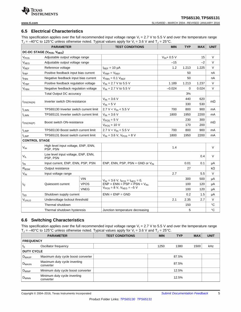
6.5 Electrical CharacteristicsThis specification applies over the full recommended input voltage range VI = 2.7 V to 5.5 V and over the temperature rangeTJ = –40°C to 125°C unless otherwise noted. Typical values apply for VI = 3.6 V and TJ = 25°C.
PARAMETER TEST CONDITIONS MIN TYP MAX UNITDC-DC STAGE (VPOS, VNEG)VPOS Adjustable output voltage range VIN+ 0.5 V 15 VVNEG Adjustable output voltage range –15 –2 VVREF Reference voltage IREF = 10 µA 1.2 1.213 1.225 VIFBP Positive feedback input bias current VFBP = VREF 50 nAIFBN Negative feedback input bias current VFBN = 0.1 VREF 50 nAVFBP Positive feedback regulation voltage VIN = 2.7 V to 5.5 V 1.189 1.213 1.237 VVFBN Negative feedback regulation voltage VIN = 2.7 V to 5.5 V –0.024 0 0.024 V
Total Output DC accuracy 3%
rDS(ON)(N) Inverter switch ON-resistanceVIN = 3.6 V 440 620
mΩVIN = 5 V 330 530
ILIMN TPS65130 Inverter switch current limit 2.7 V < VIN < 5.5 V 700 800 900 mAILIMN TPS65131 Inverter switch current limit VIN = 3.6 V 1800 1950 2200 mA
rDS(ON)(P) Boost switch ON-resistanceVPOS = 5 V 230 300
mΩVPOS = 10 V 170 200
ILIMP TPS65130 Boost switch current limit 2.7 V < VIN < 5.5 V 700 800 900 mAILIMP TPS65131 Boost switch current limit VIN = 3.6 V, VPOS = 8 V 1800 1950 2200 mACONTROL STAGE
VIHHigh level input voltage, ENP, ENN,PSP, PSN 1.4 V
VILLow level input voltage, ENP, ENN,PSP, PSN 0.4 V
IIN Input current, ENP, ENN, PSP, PSN ENP, ENN, PSP, PSN = GND or VIN 0.01 0.1 µARBSW Output resistance 27 kΩVIN Input voltage range 2.7 5.5 V
ENP = ENN = PSP = PSN = VIN,VPOS = 8 V, VNEG = –5 V
300 500 µAVPOS 100 120 µAVNEG 100 120 µA
ISD Shutdown supply current ENN = ENP = GND 0.2 1.5 µAVUVLO Undervoltage lockout threshold 2.1 2.35 2.7 V
Thermal shutdown 150 °CThermal shutdown hysteresis Junction temperature decreasing 5 °C
6.6 Switching CharacteristicsThis specification applies over the full recommended input voltage range VI = 2.7 V to 5.5 V and over the temperature rangeTJ = –40°C to 125°C unless otherwise noted. Typical values apply for VI = 3.6 V and TJ = 25°C.
PARAMETER TEST CONDITIONS MIN TYP MAX UNITFREQUENCYfS Oscillator frequency 1250 1380 1500 kHzDUTY CYCLEDMAXP Maximum duty cycle boost converter 87.5%
7.1 OverviewThe TPS6513x operates with an input voltage range of 2.7 V to 5.5 V and can generate both a positive andnegative output. Both converters work independently of each other. They only share a common clock and acommon voltage reference. Both outputs are separately controlled by a fixed-frequency, pulse-width-modulated(PWM) regulator. In general, each converter operates at continuous conduction mode (CCM). At light loads, thenegative converter can enter discontinuous conduction mode (DCM). As the load current decreases, theconverters can enter a power-save mode if enabled. This works independently at both converters. Outputvoltages can go up to 15 V at the boost output and down to –15 V at the inverter output.
7.2 Functional Block Diagram
7.3 Feature Description
7.3.1 Power ConversionBoth converters operate in a fixed-frequency, PWM control scheme. So, the ON-time of the switches variesdepending on input-to-output voltage ratio and the load. During this ON-time, the inductors connected to theconverters charge with current. In the remaining time, the time period set by the fixed operating frequency, theinductors discharge into the output capacitors through the rectifier diodes. Usually at greater loads, the inductorcurrents are continuous. At lighter loads, the boost converter uses an additional internal switch to allow currentflowing back to the input. This avoids inductor current becoming discontinuous in the boost converter. So, theboost converter is always controlled in a continuous current mode. At the inverting converter, during light loads,the inductor current can become discontinuous. In this case, the control circuit of the inverting controller outputautomatically takes care of these changing conditions to always operate with an optimum control setup.
Feature Description (continued)7.3.2 ControlThe controller circuits of both converters employ a fixed-frequency, multiple-feedforward controller topology. Thecircuits monitor input voltage, output voltage, and voltage drop across the switches. Changes in the operatingconditions of the converters directly affect the duty cycle and must not take the indirect and slow way through theoutput voltage control loops. Measurement errors in this feedforward system are corrected by a self-learningcontrol system. An external capacitor damps the output to avoid output-voltage steps due to output changes ofthis selflearning control system.
The voltage loops, determined by the error amplifiers, must only handle small signal errors. The error amplifiersfeature internal compensation. Their inputs are the feedback voltages on the FBP and FBN pins. The deviceuses a comparison of these voltages with the internal reference voltage to generate an accurate and stableoutput voltage.
7.3.3 EnableBoth converters can be enabled or disabled individually. Applying a logic HIGH signal at the enable pins (ENP forthe boost converter, ENN for the inverting converter) enables the corresponding output. After enabling, internalcircuitry, necessary to operate the specific converter, then turns on, followed by the Soft-Start.
AApplying a low signal at the enable ENP or ENN pin shuts down the corresponding converter. When bothenable pins are low, the device enters shutdown mode, where all internal circuitry turns off. The device nowconsumes shutdown current flowing into the VIN pin. The output loads of the converters can be disconnectedfrom the input, see Load Disconnect.
7.3.4 Load DisconnectThe device supports completely disconnecting the load when the converters are disabled. For the invertingconverter, the device turns off the internal PMOS switch. If the inverting converter is turned off, no DC currentpath remains which could discharge the battery or supply.
This is different for the boost converter. The external rectifying diode, together with the boost inductor, form a DCcurrent path which could discharge the battery or supply if any load connects to the output. The device has nointernal switch to prevent current from flowing. For this reason, the device offers a PMOS gate control output(BSW) to enable and disable a PMOS switch in this DC current path, ideally directly between the boost inductorand battery. To be able to fully disconnect the battery, the forward direction of the parasitic backgate diode of thisswitch must point to the battery or supply. The external PMOS switch, which connects to BSW, turns on whenthe boost converter is enabled and turns off when the boost converter is disabled.
7.3.5 Soft-StartBoth converters have implemented soft-start functions. When each converter is enabled, the implemented switchcurrent limit ramps up slowly to its nominal programmed value in about 1 ms. Soft-start is implemented to limitthe input current during start-up to avoid high peak currents at the battery which could interfere with othersystems connected to the same battery. Without soft-start, the high input peak current could trigger theimplemented switch current limit, which can lead to a significant voltage drops across the series resistance of thebattery and its connections.
7.3.6 Overvoltage ProtectionBoth converters (boost and inverter) have implemented individual overvoltage protection. If the feedback voltageunder normal operation exceeds the nominal value by typically 5%, the corresponding converter shuts downimmediately to protect any connected circuitry from possible damage.
7.3.7 Undervoltage LockoutAn undervoltage lockout (UVLO) prevents the device from starting up and operating if the supply voltage at theVIN pin is lower than the undervoltage lockout threshold. For this case, the device automatically shuts down bothconverters when the supply voltage at VIN falls below this threshold. Nevertheless, parts of the control circuitsremain active, which is different than device shutdown.
Feature Description (continued)7.3.8 Overtemperature ShutdownThe device automatically shuts down both converters if the implemented internal temperature sensor detects achip temperature above the thermal shutdown temperature. It automatically starts operating again when the chiptemperature falls below this thermal shutdown temperature. The built-in hysteresis avoids undefined operationcaused by ringing from shutdown and prevents operating at a temperature close to the overtemperatureshutdown threshold.
7.4 Device Functional Modes
7.4.1 Power-Save ModeThe power-save mode can improve efficiency at light loads. In power-save mode, the converter only operateswhen the output voltage falls below an device internally set threshold voltage. The converter ramps up the outputvoltage with one or several operating pulses and goes again into power-save mode once the inductor currentbecomes discontinuous.
The PSN and PSP logic level selects between power-save mode and continuous-conduction mode. If the specificpins (PSP for the boost converter, PSN for the inverting converter) are HIGH, the power-save mode for thecorresponding converter operates at light loads. Similarly, a LOW on the PSP pin or PSN pin disables the power-save mode for the corresponding converter.
7.4.2 Full Operation with VIN > 2.7 VThe recommended minimum input supply voltage for the TPS6513x device is 2.7 V. Above this voltage, thedevice achieves the performance described in this data sheet.
7.4.3 Limited Operation with VUVLO < VIN < 2.7 VWith input supply voltages between VUVLO and 2.7 V, the device continues to operate — no functions aredisabled — but full performance is not ensure.
7.4.4 No Operation with VIN < VUVLO
The TPS6513x enters an undervoltage lockout condition when the input supply voltage is below the UVLOthreshold. In this mode, all device functions are disabled, and the input supply current consumption is minimized.See also the Undervoltage Lockout section.
NOTEInformation in the following applications sections is not part of the TI componentspecification, and TI does not warrant its accuracy or completeness. TI’s customers areresponsible for determining suitability of components for their purposes. Customers shouldvalidate and test their design implementation to confirm system functionality.
8.1 Application InformationThe TPS6513x boost converter output voltage, VPOS, and the inverting converter output voltage, VNEG, requireexternal components to set the required output voltages. The valid output voltage ranges are as shown inRecommended Operating Conditions. The following sections show a typical application example with differentoutput voltage settings and guidance for external component choices.
8.2 Typical Application
Figure 8. Typical Application Schematic With VPOS = 10.5 V, VNEG = –10 V
L1, L2 Wurth Elektronik 7447789004 (TPS65130),EPCOS B82462-G4472 (TPS65131)
Q1 MOSFET, P-channel, 12 V, 4 A, VishaySi2323DS
8.2.2 Detailed Design ProcedureThe TPS6513x DC-DC converter is intended for systems typically powered by a single-cell Li-ion or Li-polymerbattery with a terminal voltage from 2.7 V up to 4.2 V. Because the recommended input voltage goes up to 5.5 V,the device is also suitable for 3-cell alkaline, NiCd, or NiMH batteries, as well as any regulated supply voltagesfrom 2.7 V to 5.5 V. It provides two independent output voltage rails which are programmed as follows.
8.2.2.1 Programming the Output Voltage
8.2.2.1.1 Boost Converter
The output voltage of the TPS6513x boost converter stage can be adjusted with an external resistor dividerconnected to the FBP pin. The typical value of the voltage at the FBP pin is the reference voltage, which is 1.213V. The maximum recommended output voltage at the boost converter is 15 V. To achieve appropriate accuracy,the current through the feedback divider should be about 100 times greater than the current into the FBP pin.Typical current into the FBP pin is 0.05 µA, and the voltage across R2 is 1.213 V. Based on those values, therecommended value for R2 should be lower than 200 kΩ to set the divider current at 5 µA or greater.
Calculate the value of resistor R1, as a function of the needed output voltage (VPOS), with Equation 1:
(1)
In this example, with R2 = 130 kΩ, choose R1 = 1 MΩ to set VPOS = 10.5 V.
8.2.2.1.2 Inverting Converter
The output voltage of the inverting converter stage can also be adjusted with an external resistor divider. It mustbe connected to the FBN pin. Unlike the feedback divider at the boost converter, the reference point of thefeedback divider is not GND but VREF. So the typical value of the voltage at the FBN pin is 0 V. The minimumrecommended output voltage at the inverting converter is –15 V. Feedback divider current considerations aresimilar to the considerations at the boost converter. For the same reasons, the feedback divider current shouldbe in the range of 5 µA or greater. The voltage across R4 is 1.213 V. Based on those values, the recommendedvalue for R4 should be lower than 200 kΩ to set the divider current at the required value.
Calculate the value of resistor R3, as a function of the needed output voltage (VNEG), with Equation 2:
(2)
In this example, with R4 = 121.2 kΩ, choose R3 = 1 MΩ to set VNEG = –10 V.
8.2.2.2 Inductor SelectionAn inductive converter normally requires two main passive components for storing energy during the conversion.Therefore, each converter requires an inductor and a storage capacitor. In selecting the right inductor, TIrecommends keeping the possible peak inductor current below the current limit threshold of the power switch inthe chosen configuration. To select the right inductor, TI recommends keeping the possible peak inductor currentbelow the current limit threshold of the power switch in the chosen configuration. For example, the current limitthreshold of the switch for the boost converter and for the inverting converters is nominally 800 mA for theTPS65130 device and 1950 mA for TPS65131 device. The highest peak current through the switches and theinductor depend on the output load, the input voltage (VIN), and the output voltages (VPOS, VNEG). Use Equation 3to estimate the peak inductor current in the boost converter, IL_P. Equation 4 shows the corresponding formula forthe inverting converter, IL_N.
(3)
(4)
The second parameter for choosing the inductor is the desired current ripple in the inductor. Normally, it isadvisable to work with a ripple of less than 20% of the average inductor current. A smaller ripple reduces thelosses in the inductor, as well as output voltage ripple and EMI. But in the same way, output voltage regulationgets slower, causing greater voltage changes at fast load changes. In addition, a larger inductor usuallyincreases the total system cost. Keep those parameters in mind and calculate the possible inductor value withEquation 5 for the boost converter and Equation 6 for the inverting converter.
(5)
(6)
Parameter f is the switching frequency. For the boost converter, ΔIL-P is the ripple current in the inductor, that is,20% of IL-P. Accordingly, for the inverting converter, ΔIL-N is the ripple current in the inductor, that is, 20% of IL-N.VI is the input voltage, which is 3.3 V in this example. So, the calculated inductance value for the boost inductoris 5.1 μH and for the inverting converter inductor is 5.1 μH. With these calculated values and the calculatedcurrents, it is possible to choose a suitable inductor.
In typical applications, the recommendation is to choose a 4.7-μH inductor. The device is optimized to work withinductance values from 3.3 μH to 6.8 μH. Nevertheless, operation with greater inductance values may bepossible in some applications. Perform detailed stability analysis in this case. Be aware of the possibility that loadtransients and losses in the circuit can lead to higher currents than estimated in Equation 3 and Equation 4. Also,the losses caused by magnetic hysteresis and conductor resistance are a major parameter for total circuitefficiency.
Table 3 shows inductors from different suppliers used with the TPS6513x converter:
Table 3. List of InductorsVENDOR INDUCTOR SERIES
EPCOS B8246284-G4
Wurth Elektronik7447789XXX744031XXX
TDKVLF3010VLF4012
Cooper Electronics Technologies SD12
8.2.2.3 Capacitor Selection
8.2.2.3.1 Input Capacitor
As a recommendation, choose an input capacitors of at least 4.7 μF for the input of the boost converter (INP)and accordingly for the input of the inverting converter (INN). This improves transient behavior of the regulatorsand EMI behavior of the total power-supply circuit. Choose a ceramic capacitor or a tantalum capacitor. For theuse of a tantalum capacitor, an additional, smaller ceramic capacitor (100 nF) in parallel is required. Place theinput capacitor(s) close to the input pins..
8.2.2.3.2 Output Capacitors
One of the major parameters necessary to define the capacitance value of the output capacitor is the maximumallowed output voltage ripple of the converter. This ripple is determined by two parameters of the capacitor, thecapacitance and the ESR. It is possible to calculate the minimum capacitance needed for the defined ripple,supposing that the ESR is zero. Use Equation 7 for the boost converter output capacitor (C4min) and Equation 8for the inverting converter output capacitor (C5min).
(7)
(8)
The parameter f is the switching frequency. ΔVPOS and ΔVNEG are the maximum allowed ripple voltages for eachconverter. Choosing a ripple voltage in the range of 10 mV requires a minimum capacitance of 12 μF. The totalripple is larger due to the ESR of the output capacitor. Use Equation 9 for he boost converter and Equation 10 forthe inverting converter to calculate this additional ripple component.
(9)
(10)
In this example, an additional ripple of 2 mV is the result of using a typical ceramic capacitor with an ESR in the10-mΩ range. The total ripple is the sum of the ripple caused by the capacitance and the ripple caused by theESR of the capacitor. In this example, the total ripple is 10 mV.
Load transients can create additional ripple. When the load current increases rapidly, the output capacitor mustprovide the additional current until the inductor current increases by the control loop which sets a higher ON-time(duty cycle) of the main switch. The higher duty cycle results in longer inductor charging periods. The inductanceitself also limits the rate of increase of the inductor current. When the load current decreases rapidly, the outputcapacitor must store the excess energy (stored in the inductor) until the regulator has decreased the inductorcurrent by reducing the duty cycle. TI recommends using greater capacitance values, as the foregoingcalculations show.
8.2.2.4 Rectifier Diode SelectionBoth converters (the boost and inverting converter) require rectifier diodes, D1 and D2. As a recommendation, toreduce losses, use Schottky diodes. The forward current rating needed is equal to the maximum output current.Consider that the maximum currents, IPOSmax and INEGmax, might differ for VPOS and VNEG when choosing thediodes.
8.2.2.5 External PMOS SelectionDuring shutdown, when connected to a power supply, a path from the power supply to the positive outputconducts through the inductor and an external diode. Optionally, to fully disconnect the positive output VPOSduring shutdown, add an external PMOS (Q1). The BSW pin controls the gate of the PMOS. When choosing aproper PMOS, the VGS and VGD voltage ratings must cover the input voltage range, the drain current rating mustnot be lower than the maximum input current flowing into the application, and conditions of the PMOS operatingarea must fit.
If there is no intention to use an external PMOS, leave the BSW pin floating.
8.2.2.6 Stabilizing the Control Loop
8.2.2.6.1 Feedforward Capacitor
As a recommendation, to speed up the control loop, place feedforward capacitors in the feedback divider, parallelto R1 (boost converter) and R3 (inverting converter). Equation 11 shows how to calculate the appropriate valuefor the boost converter, and Equation 12 for the inverting converter.
(11)
(12)
To avoid coupling noise into the control loop from the feedforward capacitors, the feedforward effect can bebandwith-limited by adding a series resistor. Any value from 10 kΩ to 100 kΩ is suitable. The greater theresistance, the lower the noise coupled into the control loop system.
8.2.2.6.2 Compensation Capacitors
The device features completely internally compensated control loops for both converters. The internalfeedforward system has built-in error correction which requires external capacitors. As a recommendation, use a10-nF capacitor at the CP pin of the boost converter and a 4.7-nF capacitor at the CN pin of the invertingconverter.
8.2.3 Application Curves
Figure 9. TPS65130 Efficiency vs Output Current Figure 10. TPS65131 Efficiency vs Output Current
9 Power Supply RecommendationsThe TPS6513x input voltage ranges from 2.7 V to 5.5 V. Consequently, the supply can come, for example, froma 3.3-V or 5-V rail. If the device starts into load during the Soft-Start phase, the drawn input current can be higherthan during post-start operation. Consider the application requirements when selecting the power supply. Toavoid unintended toggling of the Undervoltage Lockout, connect the TPS6513x through a low-impedance path tothe power supply.
10 Layout
10.1 Layout GuidelinesAs for all switching power supplies, the layout is an important step in the design, especially at high peak currentsand high switching frequencies. Improper layout might show the symptoms of poor line or load regulation, groundand output voltage shifts, stability issues, unsatisfying EMI behavior or worsened efficiency. Therefore, use wideand short traces for the main current paths and for the power ground tracks. The input capacitors (C1, C2, C3),output capacitors (C4, C5), the inductors (L1, L2), and the rectifying diodes (D1, D2) should be placed as closeas possible to the IC to keep parasitic inductances low. Use a wide power ground (PGND) plane. Connect theanalog ground pin (AGND) to the PGND plane. Further, connect the PGND plane with the exposed thermal pad.Place the feedback dividers as close as possible to the control pin (boost converter) or the VREF pin (invertingconverter) of the IC.
10.3 Thermal ConsiderationsImplementation of integrated circuits in low-profile and fine-pitch surface-mount packages typically requiresspecial attention to power dissipation. Many system-dependent issues, such as thermal coupling, airflow, addedheatsinks and convection surfaces, and the presence of heat-generating components affect the power-dissipation limits of a given component.
The following are three basic approaches for enhancing thermal performance follow:• Improving the power dissipation capability of the PCB design.• Improving the thermal coupling of the component to the PCB.• Introducing airflow to the system.
The recommended device junction temperature range, TJ, is –40°C to 125°C. The thermal resistance of the 24-pin QFN, 4–mm × 4–mm package (RGE) is RθJA = 34.1°C/W. The recommended operating ambient temperaturerange for the device is TA = –40°C to 85°C. Use Equation 13 to calculate the maximum power dissipation,PDmax, as a function of TA. In this equation, use TJ = 125°C to operate the device within the recommendedtemperature range, use TJ = TTS to determine the absolute maximum threshold when the device might go intothermal shutdown. If the maximum ambient temperature of the application is lower, more heat dissipation ispossible.
11.1.1 Third-Party Products DisclaimerTI'S PUBLICATION OF INFORMATION REGARDING THIRD-PARTY PRODUCTS OR SERVICES DOES NOTCONSTITUTE AN ENDORSEMENT REGARDING THE SUITABILITY OF SUCH PRODUCTS OR SERVICESOR A WARRANTY, REPRESENTATION OR ENDORSEMENT OF SUCH PRODUCTS OR SERVICES, EITHERALONE OR IN COMBINATION WITH ANY TI PRODUCT OR SERVICE.
11.2 Related LinksThe table below lists quick access links. Categories include technical documents, support and communityresources, tools and software, and quick access to sample or buy.
Table 4. Related Links
PARTS PRODUCT FOLDER SAMPLE & BUY TECHNICALDOCUMENTS
TOOLS &SOFTWARE
SUPPORT &COMMUNITY
TPS65130 Click here Click here Click here Click here Click hereTPS65131 Click here Click here Click here Click here Click here
11.3 Community ResourcesThe following links connect to TI community resources. Linked contents are provided "AS IS" by the respectivecontributors. They do not constitute TI specifications and do not necessarily reflect TI's views; see TI's Terms ofUse.
TI E2E™ Online Community TI's Engineer-to-Engineer (E2E) Community. Created to foster collaborationamong engineers. At e2e.ti.com, you can ask questions, share knowledge, explore ideas and helpsolve problems with fellow engineers.
Design Support TI's Design Support Quickly find helpful E2E forums along with design support tools andcontact information for technical support.
11.4 TrademarksPowerPAD, E2E are trademarks of Texas Instruments.All other trademarks are the property of their respective owners.
11.5 Electrostatic Discharge CautionThese devices have limited built-in ESD protection. The leads should be shorted together or the device placed in conductive foamduring storage or handling to prevent electrostatic damage to the MOS gates.
11.6 GlossarySLYZ022 — TI Glossary.
This glossary lists and explains terms, acronyms, and definitions.
12 Mechanical, Packaging, and Orderable InformationThe following pages include mechanical, packaging, and orderable information. This information is the mostcurrent data available for the designated devices. This data is subject to change without notice and revision ofthis document. For browser-based versions of this data sheet, refer to the left-hand navigation.
Images above are just a representation of the package family, actual package may vary.Refer to the product data sheet for package details.
RGE 24 VQFN - 1 mm max heightPLASTIC QUAD FLATPACK - NO LEAD
4204104/H
www.ti.com
PACKAGE OUTLINE
C
SEE TERMINALDETAIL
24X 0.30.2
2.45 0.1
24X 0.50.3
1 MAX
(0.2) TYP
0.050.00
20X 0.5
2X2.5
2X 2.5
A 4.13.9
B
4.13.9
0.30.2
0.50.3
VQFN - 1 mm max heightRGE0024BPLASTIC QUAD FLATPACK - NO LEAD
4219013/A 05/2017
PIN 1 INDEX AREA
0.08 C
SEATING PLANE
1
6 13
18
7 12
24 19
(OPTIONAL)PIN 1 ID
0.1 C A B0.05
EXPOSEDTHERMAL PAD
25 SYMM
SYMM
NOTES: 1. All linear dimensions are in millimeters. Any dimensions in parenthesis are for reference only. Dimensioning and tolerancing per ASME Y14.5M. 2. This drawing is subject to change without notice. 3. The package thermal pad must be soldered to the printed circuit board for thermal and mechanical performance.
SCALE 3.000
DETAILOPTIONAL TERMINAL
TYPICAL
www.ti.com
EXAMPLE BOARD LAYOUT
0.07 MINALL AROUND
0.07 MAXALL AROUND
24X (0.25)
24X (0.6)
( 0.2) TYPVIA
20X (0.5)
(3.8)
(3.8)
( 2.45)
(R0.05)TYP
(0.975) TYP
VQFN - 1 mm max heightRGE0024BPLASTIC QUAD FLATPACK - NO LEAD
4219013/A 05/2017
SYMM
1
6
7 12
13
18
1924
SYMM
LAND PATTERN EXAMPLEEXPOSED METAL SHOWN
SCALE:15X
NOTES: (continued) 4. This package is designed to be soldered to a thermal pad on the board. For more information, see Texas Instruments literature number SLUA271 (www.ti.com/lit/slua271).5. Vias are optional depending on application, refer to device data sheet. If any vias are implemented, refer to their locations shown on this view. It is recommended that vias under paste be filled, plugged or tented.
25
SOLDER MASKOPENING
METAL UNDERSOLDER MASK
SOLDER MASKDEFINED
EXPOSEDMETAL
METAL
SOLDER MASKOPENING
SOLDER MASK DETAILS
NON SOLDER MASKDEFINED
(PREFERRED)
EXPOSEDMETAL
www.ti.com
EXAMPLE STENCIL DESIGN
24X (0.6)
24X (0.25)
20X (0.5)
(3.8)
(3.8)
4X ( 1.08)
(0.64)TYP
(0.64) TYP
(R0.05) TYP
VQFN - 1 mm max heightRGE0024BPLASTIC QUAD FLATPACK - NO LEAD
4219013/A 05/2017
NOTES: (continued) 6. Laser cutting apertures with trapezoidal walls and rounded corners may offer better paste release. IPC-7525 may have alternate design recommendations.
25
SYMM
METALTYP
SOLDER PASTE EXAMPLEBASED ON 0.125 mm THICK STENCIL
EXPOSED PAD 25
78% PRINTED SOLDER COVERAGE BY AREA UNDER PACKAGESCALE:20X
SYMM
1
6
7 12
13
18
1924
IMPORTANT NOTICE
Texas Instruments Incorporated (TI) reserves the right to make corrections, enhancements, improvements and other changes to itssemiconductor products and services per JESD46, latest issue, and to discontinue any product or service per JESD48, latest issue. Buyersshould obtain the latest relevant information before placing orders and should verify that such information is current and complete.TI’s published terms of sale for semiconductor products (http://www.ti.com/sc/docs/stdterms.htm) apply to the sale of packaged integratedcircuit products that TI has qualified and released to market. Additional terms may apply to the use or sale of other types of TI products andservices.Reproduction of significant portions of TI information in TI data sheets is permissible only if reproduction is without alteration and isaccompanied by all associated warranties, conditions, limitations, and notices. TI is not responsible or liable for such reproduceddocumentation. Information of third parties may be subject to additional restrictions. Resale of TI products or services with statementsdifferent from or beyond the parameters stated by TI for that product or service voids all express and any implied warranties for theassociated TI product or service and is an unfair and deceptive business practice. TI is not responsible or liable for any such statements.Buyers and others who are developing systems that incorporate TI products (collectively, “Designers”) understand and agree that Designersremain responsible for using their independent analysis, evaluation and judgment in designing their applications and that Designers havefull and exclusive responsibility to assure the safety of Designers' applications and compliance of their applications (and of all TI productsused in or for Designers’ applications) with all applicable regulations, laws and other applicable requirements. Designer represents that, withrespect to their applications, Designer has all the necessary expertise to create and implement safeguards that (1) anticipate dangerousconsequences of failures, (2) monitor failures and their consequences, and (3) lessen the likelihood of failures that might cause harm andtake appropriate actions. Designer agrees that prior to using or distributing any applications that include TI products, Designer willthoroughly test such applications and the functionality of such TI products as used in such applications.TI’s provision of technical, application or other design advice, quality characterization, reliability data or other services or information,including, but not limited to, reference designs and materials relating to evaluation modules, (collectively, “TI Resources”) are intended toassist designers who are developing applications that incorporate TI products; by downloading, accessing or using TI Resources in anyway, Designer (individually or, if Designer is acting on behalf of a company, Designer’s company) agrees to use any particular TI Resourcesolely for this purpose and subject to the terms of this Notice.TI’s provision of TI Resources does not expand or otherwise alter TI’s applicable published warranties or warranty disclaimers for TIproducts, and no additional obligations or liabilities arise from TI providing such TI Resources. TI reserves the right to make corrections,enhancements, improvements and other changes to its TI Resources. TI has not conducted any testing other than that specificallydescribed in the published documentation for a particular TI Resource.Designer is authorized to use, copy and modify any individual TI Resource only in connection with the development of applications thatinclude the TI product(s) identified in such TI Resource. NO OTHER LICENSE, EXPRESS OR IMPLIED, BY ESTOPPEL OR OTHERWISETO ANY OTHER TI INTELLECTUAL PROPERTY RIGHT, AND NO LICENSE TO ANY TECHNOLOGY OR INTELLECTUAL PROPERTYRIGHT OF TI OR ANY THIRD PARTY IS GRANTED HEREIN, including but not limited to any patent right, copyright, mask work right, orother intellectual property right relating to any combination, machine, or process in which TI products or services are used. Informationregarding or referencing third-party products or services does not constitute a license to use such products or services, or a warranty orendorsement thereof. Use of TI Resources may require a license from a third party under the patents or other intellectual property of thethird party, or a license from TI under the patents or other intellectual property of TI.TI RESOURCES ARE PROVIDED “AS IS” AND WITH ALL FAULTS. TI DISCLAIMS ALL OTHER WARRANTIES ORREPRESENTATIONS, EXPRESS OR IMPLIED, REGARDING RESOURCES OR USE THEREOF, INCLUDING BUT NOT LIMITED TOACCURACY OR COMPLETENESS, TITLE, ANY EPIDEMIC FAILURE WARRANTY AND ANY IMPLIED WARRANTIES OFMERCHANTABILITY, FITNESS FOR A PARTICULAR PURPOSE, AND NON-INFRINGEMENT OF ANY THIRD PARTY INTELLECTUALPROPERTY RIGHTS. TI SHALL NOT BE LIABLE FOR AND SHALL NOT DEFEND OR INDEMNIFY DESIGNER AGAINST ANY CLAIM,INCLUDING BUT NOT LIMITED TO ANY INFRINGEMENT CLAIM THAT RELATES TO OR IS BASED ON ANY COMBINATION OFPRODUCTS EVEN IF DESCRIBED IN TI RESOURCES OR OTHERWISE. IN NO EVENT SHALL TI BE LIABLE FOR ANY ACTUAL,DIRECT, SPECIAL, COLLATERAL, INDIRECT, PUNITIVE, INCIDENTAL, CONSEQUENTIAL OR EXEMPLARY DAMAGES INCONNECTION WITH OR ARISING OUT OF TI RESOURCES OR USE THEREOF, AND REGARDLESS OF WHETHER TI HAS BEENADVISED OF THE POSSIBILITY OF SUCH DAMAGES.Unless TI has explicitly designated an individual product as meeting the requirements of a particular industry standard (e.g., ISO/TS 16949and ISO 26262), TI is not responsible for any failure to meet such industry standard requirements.Where TI specifically promotes products as facilitating functional safety or as compliant with industry functional safety standards, suchproducts are intended to help enable customers to design and create their own applications that meet applicable functional safety standardsand requirements. Using products in an application does not by itself establish any safety features in the application. Designers mustensure compliance with safety-related requirements and standards applicable to their applications. Designer may not use any TI products inlife-critical medical equipment unless authorized officers of the parties have executed a special contract specifically governing such use.Life-critical medical equipment is medical equipment where failure of such equipment would cause serious bodily injury or death (e.g., lifesupport, pacemakers, defibrillators, heart pumps, neurostimulators, and implantables). Such equipment includes, without limitation, allmedical devices identified by the U.S. Food and Drug Administration as Class III devices and equivalent classifications outside the U.S.TI may expressly designate certain products as completing a particular qualification (e.g., Q100, Military Grade, or Enhanced Product).Designers agree that it has the necessary expertise to select the product with the appropriate qualification designation for their applicationsand that proper product selection is at Designers’ own risk. Designers are solely responsible for compliance with all legal and regulatoryrequirements in connection with such selection.Designer will fully indemnify TI and its representatives against any damages, costs, losses, and/or liabilities arising out of Designer’s non-compliance with the terms and provisions of this Notice.