Contents lists available at SciVerse ScienceDirect
Sensors and Actuators B: Chemical
j o ur nal homep a ge: www.elsev ier .com/ locate /snb
O2 gas sensor fabrication through AC electrophoretic deposition fromlectrospun In2O3 nanoribbons
. Sowti Khiabania, A. Hosseinmardib, E. Marzbanrada,∗, S. Ghashghaiea, C. Zamanic,. Keyanpour-Radd, B. Raissib
Department of Ceramic, Materials and Energy Research Center, Karaj, IranDepartment of Nano and Advanced Materials, Materials and Energy Research Center, Karaj, IranXaRMAE/IN2UB, Department of Electronica, Universitat de Barcelona, 08028 Barcelona, SpainDepartment of Energy, Materials and Energy Research Center, Karaj, Iran
r t i c l e i n f o
rticle history:eceived 20 July 2011eceived in revised form5 December 2011ccepted 16 December 2011vailable online 24 December 2011
a b s t r a c t
In this paper, electrospinning method was employed to fabricate polymer–ceramic composite fibersfrom solutions containing polyvinyl pyrrolidone (PVP) and In(NO3)3·xH2O. Upon firing the compositefibers at 600 ◦C, In2O3 nanoribbons with cross section around 250 nm were synthesized. Gas sensor wasfabricated by deposition of In2O3 nanoribbons between the electrodes via AC electrophoretic deposition.Gas sensing measurements showed that this material has high response to very low concentrations ofNO2 gas at 200 ◦C.
eywords:n2O3
lectrospinninganoribbonC electrophoretic depositionO2 gas sensor
Indium oxide (In2O3) is known to be a wide band gap (∼2.9 eV)-type semiconductor in its nonstoichiometric form, due to intrin-ic oxygen vacancies responsible for electron conductivity [1].
Chemisorption of oxygen under ambient conditions createsxtrinsic acceptor states that repel conduction band electrons andesult in the formation of depletion layer. In polycrystalline sens-ng materials these depletion layers act as a potential barrier inrain boundaries and electrons have to overcome these barriers toow through the material which leads to a decrease in electroniconductivity of the material. In nano-scale size materials (withiameter less than Debye length) these barriers are eliminated andhe gas sensitivity of the sensor is increased [2]. In this regard,
any researches have been done in order to obtain zero dimen-ional In2O3 nanostructures, such as nanospheres [3], nanocubes4] and 1-dimensional In2O3 nanostructures such as nanorods [5],
anowires [6,7], nanobelts [8], nanofibers [9], and nanotubes [10].anospheres, as zero-dimensional (0D) nanostructures, have a high
endency to form hard aggregates, a phenomenon which limits gas
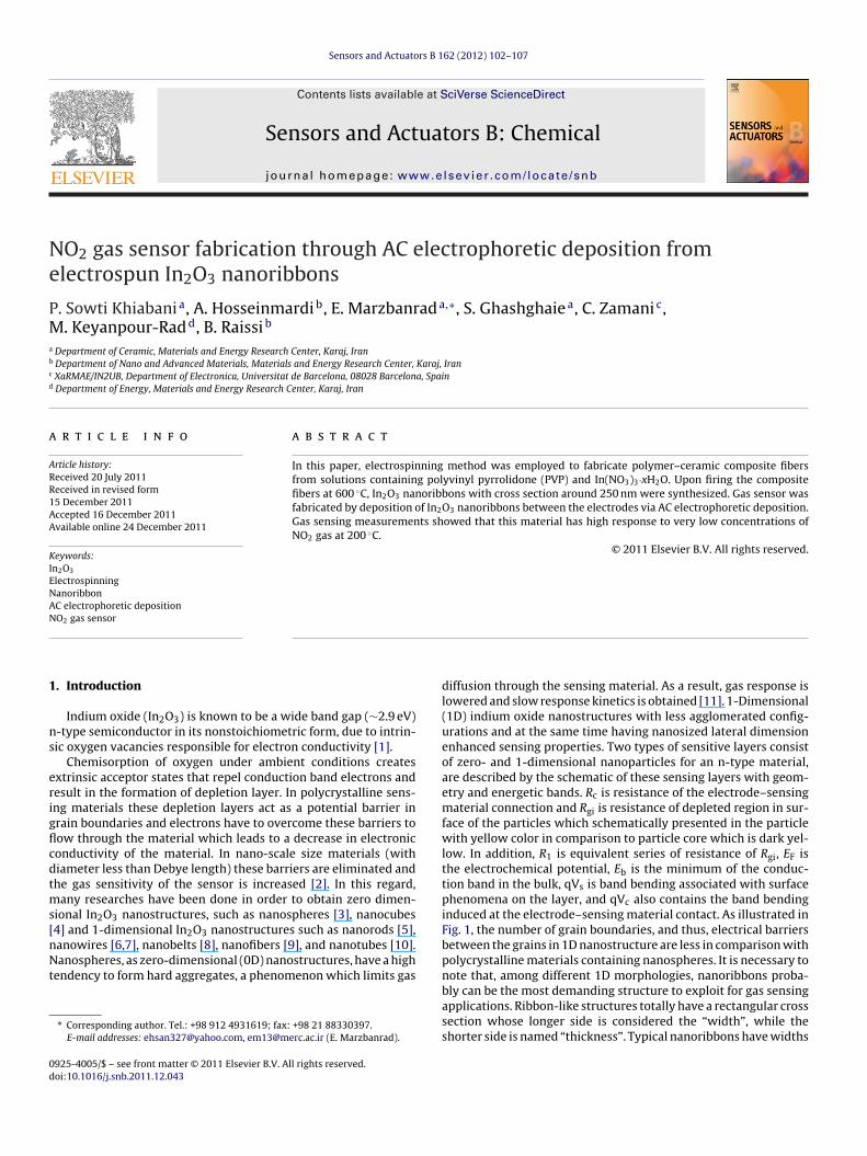
diffusion through the sensing material. As a result, gas response islowered and slow response kinetics is obtained [11]. 1-Dimensional(1D) indium oxide nanostructures with less agglomerated config-urations and at the same time having nanosized lateral dimensionenhanced sensing properties. Two types of sensitive layers consistof zero- and 1-dimensional nanoparticles for an n-type material,are described by the schematic of these sensing layers with geom-etry and energetic bands. Rc is resistance of the electrode–sensingmaterial connection and Rgi is resistance of depleted region in sur-face of the particles which schematically presented in the particlewith yellow color in comparison to particle core which is dark yel-low. In addition, R1 is equivalent series of resistance of Rgi, EF isthe electrochemical potential, Eb is the minimum of the conduc-tion band in the bulk, qVs is band bending associated with surfacephenomena on the layer, and qVc also contains the band bendinginduced at the electrode–sensing material contact. As illustrated inFig. 1, the number of grain boundaries, and thus, electrical barriersbetween the grains in 1D nanostructure are less in comparison withpolycrystalline materials containing nanospheres. It is necessary tonote that, among different 1D morphologies, nanoribbons proba-
bly can be the most demanding structure to exploit for gas sensingapplications. Ribbon-like structures totally have a rectangular crosssection whose longer side is considered the “width”, while theshorter side is named “thickness”. Typical nanoribbons have widths
ig. 1. Schematic representation of the sensing layer consisting of (a) zero-imensional and (b) 1-dimensional sensing material with energy bands.
n the range of 20–300 nm, and lengths from several hundreds,r even some thousands of micrometers with width-to-thicknessatio of about 5–10. However, for nanowires (or nanorods) thisatio equals to 2–5. Although nanoribbons are not mechanically astrong as nanotubes, they offer structural homogeneity and crystal-ographic perfection. It is well known that crystallographic defects
ay diminish quantum-size effects as it is the case for nanowires.his limiting does not arise in nanoribbons because of their per-ect crystal structure. It is necessary to emphasize that the suitableeometry, high homogeneity of the structure, and long length aremportant advantages of nanoribbons for mass production of higherformance gas sensors. Besides, nanoribbons have flexible struc-ures, and, therefore, they could be curved up to 180◦ without beingamaged, a property which is hardly observed in other types of 1Danostructures. This fact gives additional advantages to nanorib-ons for sensor designing [12].
Synthesis of nanoribbons can be conducted via various meth-ds which provide considerable opportunities for research on suchanosized materials. Electrospinning has been commonly used as
simple and versatile method for preparing ceramic nanoribbonsncluding In2O3. Unique properties of ultrafine fiber membranesrepared by electrospinning process, such as high porosity withmall and continuous pores and high surface area to volume ratio,ave extended research interest in potential applications of thisat in filter media, energy conversion and storage, biomedical
pplications, sensor, etc. [13–15].In a typical electrospinning process, under the effect of high-
oltage, the jet of precursors ejects from the tip of needle towardhe collector [16]. As a result, the jet whips rapidly and the sol-ent evaporates forming a nonwoven fibrous mat on the collector.heng et al. investigated the gas sensing properties of electrospunn2O3 nanofibers and reported excellent ethanol-sensing charac-eristics [9,10]. Also, Xu et al. reported high response to H2S at roomemperature for electrospun In2O3 nanowires [10].
The assembly of nanoparticles into ordered arrays is critical tohe realization of integrated electronic architectures. Application oflectric field is a powerful tool for self-alignment of nanoparticles
nto a well-defined space region, in which an external electric fields induced, requiring no mechanical nanomanipulation techniques17]. Very recently, we employed AC electrophoresis for manipulat-ng semiconducting and oxide nanostructures to obtain prototype
ctuators B 162 (2012) 102– 107 103
devices [18–20] where it was shown that thick, porous and wellaligned layers with desirable sensitivity, comparable with otherworks, can be obtained via this method.
In the current work, In2O3 nanoribbons were first synthe-sized by the electrospinning method followed by employing ACelectrophoretic deposition technique to deposit the nanoribbons.Finally, the gas sensing properties of the fabricated nanoribbonstoward NO2 as an oxidizing gas were investigated.
2. Experimental
Indium nitrate (In(NO3)3·xH2O), ethanol and N,N-dimethylformamide (DMF) purchased from Merck and poly(vinylpyrrolidone) (PVP, Mw = 1,300,000) obtained from Aldrich, wereused to prepare the starting solution. At the next step, 0.4 gIn(NO3)3·xH2O powder was added to 8.8 g of the mixed solvent,containing DMF/ethanol with the weight ratio of 1:3 and stirredfor 2 h. 0.8 g PVP was added to the resulting solution and stirredfor further 6 h. The resulting solution was then loaded into a50 ml plastic syringe with stainless steel needle (inner diameter of0.495 mm, 21 G, and length of 0.5 in.) connected to a high-voltagesupply (Glassman High Voltage Inc.), which is capable of generat-ing high direct current (DC). In our experiment, a voltage of 15 kVwas applied for electrospinning the solution. An aluminum platewas used as the collector and the distance between the capillaryand the collector was set at 15 cm. The feed rate was controlledby an electrical syringe pump (Top 5300) fixed at 1.5 ml/h. Theas-electrospun PVP/In(NO3)3·xH2O composite nanofibers wereplaced in vacuum at room temperature for 12 h in order to removethe solvent residuals, and then calcined in air at 600 ◦C for 3 h witha heating rate of about 5 ◦C/min to obtain a yellowish product(In2O3 ceramic nanoribbons).
The X-ray diffraction (XRD) patterns of the In2O3 nanostruc-tures were recorded by Unisantis-XMD300 system with Cu K�1(� = 0.154056 nm) radiation with 2� ranging between 10 and 80◦
with step size of 0.02◦. The microstructure of the obtained depositwas analyzed using scanning electron (Cambridge, S360) and opti-cal (Olympus DP72) microscopy. The average diameter of the fibersand nanoribbons were obtained by measuring 50 fibers on SEMimages, using Image J software.
For sensor fabrication, interdigitated platinum electrodes witha gap of 200 �m designed on an alumina sheet were used. Thisalumina-based sensor was equipped with a micro heater whichwas printed on the backside of the sensor.
The In2O3 nanoribbons were then deposited on interdigitatedelectrodes by AC electrophoretic deposition. The deposition set-up consisted of a signal generator (Rigol, DG1022) and a voltageamplifier (HP, 6826A Signal Amplifier). AC electrophoretic deposi-tion was performed at frequency of 10 kHz by a symmetric sinusoidwave.
Gas sensing properties of the sensor toward NO2 gas in the tem-perature range of 150–300 ◦C were measured by using a normaldynamic gas sensing set-up.
3. Results and discussion
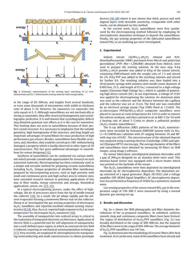
Fig. 2a–c shows the SEM photographs and fiber diameter dis-tributions of the as-prepared nanofibers. As exhibited, uniform,smooth, long and continuous composite fibers have been formed.The region of distribution of In2O3/PVP nanofibers (Fig. 2c) wasbroadly distributed in the range of 300–800 nm, but the majority
of the fibers were in the range of 450–600 nm. The average diameterof In2O3/PVP nanofibers was 547 nm.
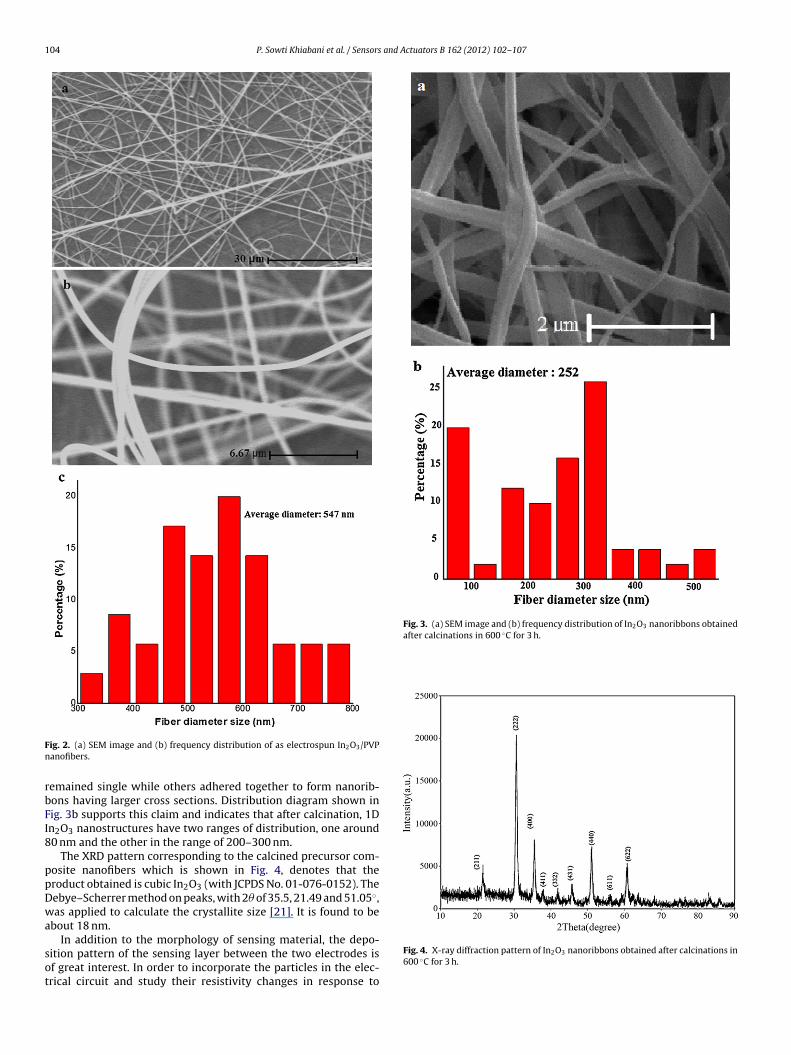
Fig. 3a demonstrates the morphology of ceramic fibers after heattreatment. As it can be seen, some of the nanofibers have shrunk and
104 P. Sowti Khiabani et al. / Sensors and Actuators B 162 (2012) 102– 107
Fn
rbFI8
ppDwa
sot
Fig. 3. (a) SEM image and (b) frequency distribution of In2O3 nanoribbons obtainedafter calcinations in 600 ◦C for 3 h.
ig. 2. (a) SEM image and (b) frequency distribution of as electrospun In2O3/PVPanofibers.
emained single while others adhered together to form nanorib-ons having larger cross sections. Distribution diagram shown inig. 3b supports this claim and indicates that after calcination, 1Dn2O3 nanostructures have two ranges of distribution, one around0 nm and the other in the range of 200–300 nm.
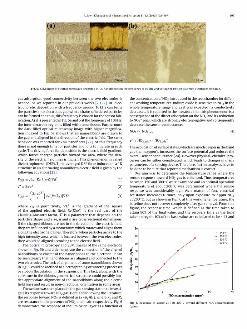
The XRD pattern corresponding to the calcined precursor com-osite nanofibers which is shown in Fig. 4, denotes that theroduct obtained is cubic In2O3 (with JCPDS No. 01-076-0152). Theebye–Scherrer method on peaks, with 2� of 35.5, 21.49 and 51.05◦,as applied to calculate the crystallite size [21]. It is found to be
bout 18 nm.
In addition to the morphology of sensing material, the depo-
ition pattern of the sensing layer between the two electrodes isf great interest. In order to incorporate the particles in the elec-rical circuit and study their resistivity changes in response to
Fig. 4. X-ray diffraction pattern of In2O3 nanoribbons obtained after calcinations in600 ◦C for 3 h.
P. Sowti Khiabani et al. / Sensors and Actuators B 162 (2012) 102– 107 105
the fr
gnttcrttttbtcwsdsf
F
�
F
woCpItaht
snbtiocdfi
gtad
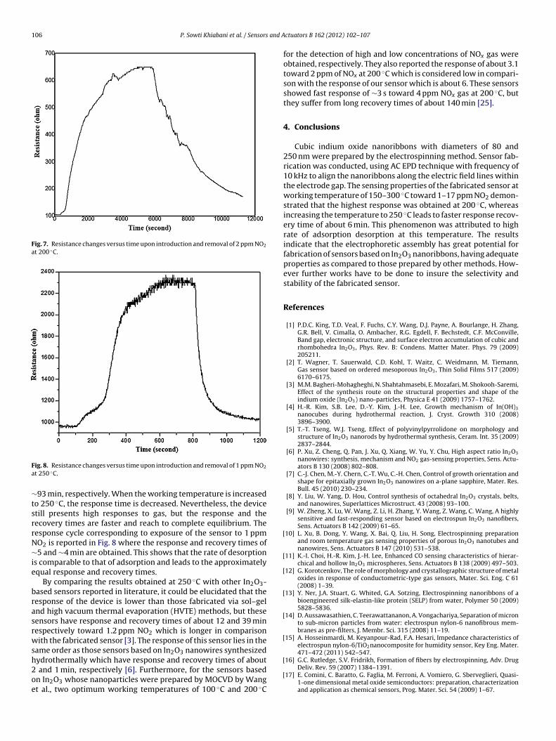
baseline does not recover completely after gas removal. From thisfigure, the response time, which is defined as the time taken toattain 90% of the final value, and the recovery time as the timetaken to regain 10% of the base value, are calculated to be ∼43 and
Fig. 5. SEM image of electrophoretically deposited In2O3 nanoribbons in
as adsorption, good connectivity between the two electrodes iseeded. As we reported in our previous works [20,22], AC elec-rophoretic deposition with a frequency around 10 kHz can bringhe particles into electrodes gap where chains of ordered particlesan be formed and thus, this frequency is chosen for the sensor fab-ication. As it is presented in Fig. 5a and b at the frequency of 10 kHz,he inter electrode region is filled with nanoribbons. Furthermorehe dark filled optical microscopy image with higher magnifica-ion indexed to Fig. 5a shows that all nanoribbons are drawn tohe gap and aligned in the direction of the electric field. The sameehavior was reported for ZnO nanofibers [22]. At this frequencyhere is not enough time for particles and ions to migrate in eachycle. The driving force for deposition is the electric field gradient,hich forces charged particles toward the area, where the den-
ity of the electric field lines is higher. This phenomenon is calledielectrophoresis (DEP). Time-averaged DEP force induced on a 1Dtructure in an alternating nonuniform electric field is given by theollowing equations [23]:
DEP = �εm[Re(k(ω))]∇E2 (1)
= 2�a3 (2)
DEP =(
2�ab2
3
)εm[Re(k˛)]∇E2 (3)
here εm is permittivity, ∇E2 is the gradient of the squaref the applied electric field, Re[K(ω)] is the real part of thelausius–Mossotti factor, � is a parameter that depends on thearticle’s shape and size, a and b are cross sectional dimensions.
f the charged ribbons are not in the direction of the electric field,hey are influenced by a momentum which rotates and aligns themlong the electric field lines. Therefore, when particles arrive to theigh intensity area, which is located between the two electrodes,hey would be aligned according to the electric field.
The optical microscopy and SEM images of the same electrodehown in Fig. 5b and d demonstrate the connection of the alignedanoribbons or cluster of the nanoribbons to the electrode. It cane seen clearly that nanoribbons are aligned and connected to thewo electrodes. The lack of alignment of some nanoribbons shownn Fig. 5, could be ascribed to electrospinning or sintering processesr ribbon flocculation in the suspension. This fact, along with theurvature in the ribbons geometrical structure, could possibly hin-er appropriate alignment of the nanoribbons along the electriceld lines and result in non-directional orientation in some areas.
The sensor was then placed in the gas sensing station to investi-
ate its response toward NO2 gas. Here, and following the literature,he response toward NO2 is defined as (S = Rg/Ra), where Rg and Ra
re resistance in the presence of NO2 and in air, respectively. Fig. 6emonstrates the response of indium oxide layer as a function of
equency of 10 kHz and voltage of 10 V on platinum electrodes for 5 min.
the concentration of NO2 introduced in the test chamber for differ-ent working temperatures. Indium oxide is sensitive to NO2 in thewhole temperature range and as it was expected its conductivitydecreases. It is reported in the literature that this phenomenon is aconsequence of the direct adsorption on the NO2 and its reductionto NO2
− ions, which are strongly electronegative and consequentlydecrease the sensor conductance:
NO2 ↔ NO2,ads (4)
e− + NO2,ads ↔ NO2,ads−
The occupation of surface states, which are much deeper in the bandgap than oxygen’s, increases the surface potential and reduces theoverall sensor conductance [24]. However physical–chemical pro-cesses can be rather complicated, which leads to changes in manyparameters of a sensing device. Therefore, further analyses have tobe done to be sure that reported mechanism is correct.
Our aim was to determine the temperature range where thesensor response toward NO2 gas is enhanced. Thus temperaturesbetween 150 and 300 ◦C were examined and an optimal operationtemperature of about 200 ◦C was determined where the sensorresponse was considerably high. As a matter of fact, electricalresistance increases 6 times, only upon exposure to 2 ppm NO2at 200 ◦C, but as shown in Fig. 7, at this working temperature, the
Fig. 6. Response of sensor at 150–300 ◦C toward different NO2 concentrations(ppm).
Fig. 7. Resistance changes versus time upon introduction and removal of 2 ppm NO2
at 200 ◦C.
Fa
∼tsrrN∼ie
brasrwsh2oe
[
[
[
[
[
[
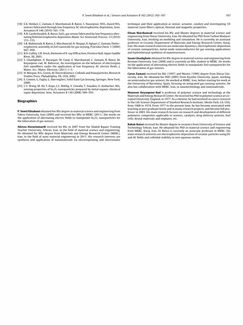
ig. 8. Resistance changes versus time upon introduction and removal of 1 ppm NO2
t 250 ◦C.
93 min, respectively. When the working temperature is increasedo 250 ◦C, the response time is decreased. Nevertheless, the devicetill presents high responses to gas, but the response and theecovery times are faster and reach to complete equilibrium. Theesponse cycle corresponding to exposure of the sensor to 1 ppmO2 is reported in Fig. 8 where the response and recovery times of5 and ∼4 min are obtained. This shows that the rate of desorption
s comparable to that of adsorption and leads to the approximatelyqual response and recovery times.
By comparing the results obtained at 250 ◦C with other In2O3-ased sensors reported in literature, it could be elucidated that theesponse of the device is lower than those fabricated via sol–gelnd high vacuum thermal evaporation (HVTE) methods, but theseensors have response and recovery times of about 12 and 39 minespectively toward 1.2 ppm NO2 which is longer in comparisonith the fabricated sensor [3]. The response of this sensor lies in the
ame order as those sensors based on In2O3 nanowires synthesized
ydrothermally which have response and recovery times of about
and 1 min, respectively [6]. Furthermore, for the sensors basedn In2O3 whose nanoparticles were prepared by MOCVD by Wangt al., two optimum working temperatures of 100 ◦C and 200 ◦C
[
[
ctuators B 162 (2012) 102– 107
for the detection of high and low concentrations of NOx gas wereobtained, respectively. They also reported the response of about 3.1toward 2 ppm of NOx at 200 ◦C which is considered low in compari-son with the response of our sensor which is about 6. These sensorsshowed fast response of ∼3 s toward 4 ppm NOx gas at 200 ◦C, butthey suffer from long recovery times of about 140 min [25].
4. Conclusions
Cubic indium oxide nanoribbons with diameters of 80 and250 nm were prepared by the electrospinning method. Sensor fab-rication was conducted, using AC EPD technique with frequency of10 kHz to align the nanoribbons along the electric field lines withinthe electrode gap. The sensing properties of the fabricated sensor atworking temperature of 150–300 ◦C toward 1–17 ppm NO2 demon-strated that the highest response was obtained at 200 ◦C, whereasincreasing the temperature to 250 ◦C leads to faster response recov-ery time of about 6 min. This phenomenon was attributed to highrate of adsorption desorption at this temperature. The resultsindicate that the electrophoretic assembly has great potential forfabrication of sensors based on In2O3 nanoribbons, having adequateproperties as compared to those prepared by other methods. How-ever further works have to be done to insure the selectivity andstability of the fabricated sensor.
References
[1] P.D.C. King, T.D. Veal, F. Fuchs, C.Y. Wang, D.J. Payne, A. Bourlange, H. Zhang,G.R. Bell, V. Cimalla, O. Ambacher, R.G. Egdell, F. Bechstedt, C.F. McConville,Band gap, electronic structure, and surface electron accumulation of cubic andrhombohedra In2O3, Phys. Rev. B: Condens. Matter Mater. Phys. 79 (2009)205211.
[2] T. Wagner, T. Sauerwald, C.D. Kohl, T. Waitz, C. Weidmann, M. Tiemann,Gas sensor based on ordered mesoporous In2O3, Thin Solid Films 517 (2009)6170–6175.
[3] M.M. Bagheri-Mohagheghi, N. Shahtahmasebi, E. Mozafari, M. Shokooh-Saremi,Effect of the synthesis route on the structural properties and shape of theindium oxide (In2O3) nano-particles, Physica E 41 (2009) 1757–1762.
[4] H.-R. Kim, S.B. Lee, D.-Y. Kim, J.-H. Lee, Growth mechanism of In(OH)3
nanocubes during hydrothermal reaction, J. Cryst. Growth 310 (2008)3896–3900.
[5] T.-T. Tseng, W.J. Tseng, Effect of polyvinylpyrrolidone on morphology andstructure of In2O3 nanorods by hydrothermal synthesis, Ceram. Int. 35 (2009)2837–2844.
[6] P. Xu, Z. Cheng, Q. Pan, J. Xu, Q. Xiang, W. Yu, Y. Chu, High aspect ratio In2O3
nanowires: synthesis, mechanism and NO2 gas-sensing properties, Sens. Actu-ators B 130 (2008) 802–808.
[7] C.-J. Chen, M.-Y. Chern, C.-T. Wu, C.-H. Chen, Control of growth orientation andshape for epitaxially grown In2O3 nanowires on a-plane sapphire, Mater. Res.Bull. 45 (2010) 230–234.
[8] Y. Liu, W. Yang, D. Hou, Control synthesis of octahedral In2O3 crystals, belts,and nanowires, Superlattices Microstruct. 43 (2008) 93–100.
[9] W. Zheng, X. Lu, W. Wang, Z. Li, H. Zhang, Y. Wang, Z. Wang, C. Wang, A highlysensitive and fast-responding sensor based on electrospun In2O3 nanofibers,Sens. Actuators B 142 (2009) 61–65.
10] L. Xu, B. Dong, Y. Wang, X. Bai, Q. Liu, H. Song, Electrospinning preparationand room temperature gas sensing properties of porous In2O3 nanotubes andnanowires, Sens. Actuators B 147 (2010) 531–538.
11] K.-I. Choi, H.-R. Kim, J.-H. Lee, Enhanced CO sensing characteristics of hierar-chical and hollow In2O3 microspheres, Sens. Actuators B 138 (2009) 497–503.
12] G. Korotcenkov, The role of morphology and crystallographic structure of metaloxides in response of conductometric-type gas sensors, Mater. Sci. Eng. C 61(2008) 1–39.
13] Y. Ner, J.A. Stuart, G. Whited, G.A. Sotzing, Electrospinning nanoribbons of abioengineered silk-elastin-like protein (SELP) from water, Polymer 50 (2009)5828–5836.
14] D. Aussawasathien, C. Teerawattananon, A. Vongachariya, Separation of micronto sub-micron particles from water: electrospun nylon-6 nanofibrous mem-branes as pre-filters, J. Membr. Sci. 315 (2008) 11–19.
15] A. Hosseinmardi, M. Keyanpour-Rad, F.A. Hesari, Impedance characteristics ofelectrospun nylon-6/TiO2nanocomposite for humidity sensor, Key Eng. Mater.471–472 (2011) 542–547.
16] G.C. Rutledge, S.V. Fridrikh, Formation of fibers by electrospinning, Adv. DrugDeliv. Rev. 59 (2007) 1384–1391.
17] E. Comini, C. Baratto, G. Faglia, M. Ferroni, A. Vomiero, G. Sberveglieri, Quasi-1-one dimensional metal oxide semiconductors: preparation, characterizationand application as chemical sensors, Prog. Mater. Sci. 54 (2009) 1–67.
and A
[
[
[
[
[
[
[
[
B
PTtt
ATHIs
Babak Raissi received his Master degree in ceramics from University of Science and
P. Sowti Khiabani et al. / Sensors
18] E.K. Heidari, C. Zamani, E. Marzbanrad, B. Raissi, S. Nazarpour, WO3-based NO2
sensors fabricated through low frequency AC electrophoretic deposition, Sens.Actuators B 146 (2010) 165–170.
19] A.R. Gardeshzadeh, B. Raissi, SnO2 gas sensor fabricated by low frequency alter-nating field electrophoretic deposition, Mater. Sci. Semicond. Process. 13 (2010)151–155.
20] S.R. Mahmoodi, B. Raissi, E. Marzbanrad, N. Shojayi, A. Aghaei, C. Zamani, Dielec-trophoretic assembly of ZnO nanorods for gas sensing, Procedia Chem. 1 (2009)947–950.
21] B.D. Cullity, S.R. Stock, Elements of X-ray Diffraction, Prentice Hall, Upper SaddleRiver, NJ, 2001.
22] S. Ghashghaie, A. Bazargan, M. Ganji, E. Marzbanrad, C. Zamani, B. Raissi, M.Keyanpour-rad, M. Bahrevar, An investigation on the behavior of electrospunZnO nanofibers under the application of low frequency AC electric fields, J.Mater. Sci.: Mater. Electron. (2011) 1–5.
23] H. Morgan, N.G. Green, AC Electrokinetics: Colloids and Nanoparticles, ResearchStudies Press, Philadelphia, PA, USA, 2002.
24] E. Comini, G. Faglia, G. Sberveglieri, Solid State Gas Sensing, Springer, New York,2008.
25] C.Y. Wang, M. Ali, T. Kups, C.C. Röhlig, V. Cimalla, T. Stauden, O. Ambacher, NOx
sensing properties of In2O3 nanoparticles prepared by metal organic chemicalvapor deposition, Sens. Actuators B 130 (2008) 589–593.
iographies
. Sowti Khiabani obtained her BSc degree in material science and engineering fromabriz University, Iran (2009) and received her MSc in MERC (2011). She works onhe application of alternating electric fields to manipulate In2O3 nanoparticles forhe fabrication of gas sensors.
lireza Hosseinmardi received his BSc in 2007 from the Shahid Rajaee Trainingeacher University, Tehran, Iran, in the field of material science and engineering.e obtained his MSc degree from Materials and Energy Research Center (MERC),
ran, in the field of nano material engineering in 2011. His research interests areynthesis and application of nanomaterials via electrospinning and electrostatic
ctuators B 162 (2012) 102– 107 107
technique and their application as sensor, actuator, catalyst and investigating 1Dmaterial (nano fibers) optical, thermal and magnetic properties.
Ehsan Marzbanrad received his BSc and Master degrees in material science andengineering from Shiraz University, Iran. He obtained his PhD from Tarbiat ModaresUniversity, Iran, working on modeling and simulation. He is currently an assistantprofessor in Ceramic Department of Materials and Energy Research Center, Karaj,Iran. His main research interests are molecular dynamics, electrophoretic depositionof ceramic nanoparticles, metal oxide semiconductors for gas sensing applicationsand hydrothermal synthesis of nanostructures.
Sasan Ghashghaie obtained his BSc degree in material science and engineering fromKerman University, Iran (2008) and is currently an MSc student in MERC. He workson the application of alternating electric fields to manipulate ZnO nanoparticles forthe fabrication of gas sensors.
Cyrus Zamani received his BSc (1997) and Master (1999) degree from Shiraz Uni-versity, Iran. He obtained his PhD (2005) from Kyushu University, Japan, workingon semiconductor gas sensors. He worked at RMRC, Iran, before starting his work atthe University of Barcelona, Spain, focusing on integrated gas-sensing systems. Healso has collaboration with MERC, Iran, in nanotechnology and nanomaterials.
Mansour Keyanpour-Rad is professor of polymer science and technology at theMaterials and Energy Research Center. He received his PhD in polymer science at Liv-erpool University, England, in 1977. As a chemist, he had involved in cancer researchin the Life Science Department of Stanford Research Institute, Menlo Park, CA, USA,from 1968 to 1974. From 1977 to the present time, he has become associated withteaching at post graduate levels and in many research projects, and become full pro-fessor in 2003. His main research focuses on research and development of differentpolymeric composites applicable in sensors, catalysts, drug delivery systems, fuelcells, dental materials and implants, etc.
Technology Tehran, Iran. He obtained his PhD in material science and engineeringfrom MERC, Karaj, Iran. Dr Raissi is currently an associate professor in MERC. Hismain research interests are electrophoretic deposition of ceramic particles using DCand AC fields and colloidal stability in non-aqueous media.