2011 ITRS Emerging Research Devices Working Group Face – to – Face Meeting. Jim Hutchby – Facilitating San Francisco Marriott Hotel 55 Fourth Street Room – Salon 5 San Francisco, California Sunday July 10, 2011 9:00 a.m. – 6:00 p.m. Emerging Research Devices Working Group. - PowerPoint PPT Presentation
30
Work in Progress --- Not for Publication 1 ERD WG 7/10/2011 San Francisco, CA. FxF Meeting 2011 ITRS Emerging Research Devices Working Group Face – to – Face Meeting Jim Hutchby – Facilitating San Francisco Marriott Hotel 55 Fourth Street Room – Salon 5 San Francisco, California Sunday July 10, 2011 9:00 a.m. – 6:00 p.m.
Transcript
Work in Progress --- Not for Publication1 ERD WG 7/10/2011 San Francisco, CA. FxF Meeting
2011 ITRS Emerging Research Devices
Working Group
Face – to – Face Meeting
Jim Hutchby – FacilitatingSan Francisco Marriott Hotel
55 Fourth StreetRoom – Salon 5
San Francisco, CaliforniaSunday July 10, 20119:00 a.m. – 6:00 p.m.
2 ERD WG 7/10/2011 San Francisco, CA. FxF Meeting
Hiroyugi Akinaga AIST Tetsuya Asai Hokkaido U. Yuji Awano Keio U. George Bourianoff Intel Michel Brillouet CEA/LETI Joe Brewer U. Florida John Carruthers PSU Ralph Cavin SRC An Chen GLFOUNDRIES U-In Chung Samsung Byung Jin Cho KAIST Sung Woong Chung Hynix Luigi Colombo TI Shamik Das Mitre Erik DeBenedictis SNL Simon Deleonibus LETI Bob Fontana IBM Paul Franzon NCSU Akira Fujiwara NTT Christian Gamrat CEA Mike Garner Intel Dan Hammerstrom PSU Wilfried Haensch IBM Tsuyoshi Hasegawa NIMS Shigenori Hayashi Matsushita Dan Herr SRC Toshiro Hiramoto U. Tokyo Matsuo Hidaka ISTEK Jim Hutchby SRC Adrian Ionescu EPFL Kiyoshi Kawabata Renesas Tech Seiichiro Kawamura Selete Suhwan Kim Seoul Nation U Hyoungjoon Kim Samsung
Atsuhiro Kinoshita Toshiba Dae-Hong Ko Yonsei U. Hiroshi Kotaki Sharp Mark Kryder INSIC Zoran Krivokapic GLOBALFOUNDRIES Kee-Won Kwon Seong Kyun Kwan U.Jong-Ho Lee Hanyang U. Lou Lome IDA Hiroshi Mizuta U. Southampton Kwok Ng SRC Fumiyuki Nihei NEC Ferdinand Peper NICT Yaw Obeng NIST Dave Roberts Nantero Barry Schechtman INSIC Sadas Shankar Intel Atsushi Shiota JSR Micro Satoshi Sugahara Tokyo Tech Shin-ichi Takagi U. Tokyo Ken Uchida Toshiba Thomas Vogelsang Rambus Yasuo Wada Toyo U. Rainer Waser RWTH A Franz Widdershoven NXP Jeff Welser NRI/IBM Philip Wong Stanford U. Dirk Wouters IMEC Kojiro Yagami Sony David Yeh SRC/TI Hiroaki Yoda Toshiba In-K Yoo SAIT Victor Zhirnov SRC
Emerging Research Devices Working Group
Work in Progress --- Not for Publication3 ERD WG 7/10/2011 San Francisco, CA. FxF Meeting
Emerging Research Devices Working Group Meeting Objectives
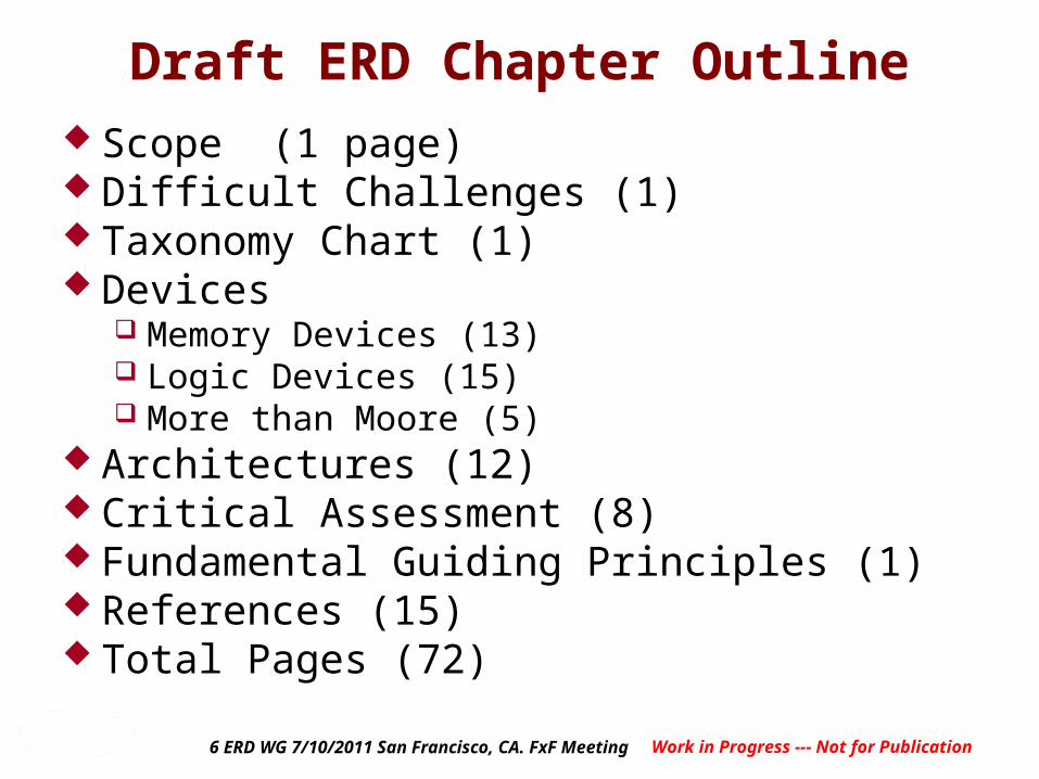
Deliverables and revised time line Chapter outline and page count
Review the Emerging Memory, Logic & Architecture Sections Table Content (Current & projected tables) Major device research needs & technical barriers Key materials scientific and/or technological issues Thrust, tone & structure of the draft section
Critical Review Section Review the Difficult Challenges Section Review Scope and Taxonomy Sections Review content of the Guiding Principles Section Decide messages for the Public Presentation
Work in Progress --- Not for Publication4 ERD WG 7/10/2011 San Francisco, CA. FxF Meeting
ITRS ERD WG Meeting – July 10, 2011Agenda
8:30 Light Continental Breakfast 9:00 Welcome and Introductions 9:10 Review meeting objectives & agenda Hutchby 9:30 Review status of ERD Chapter Hutchby
Deliverables and Timeline Chapter Organization & Status Decisions made
9:45 Complete Memory, Logic, More-than-Moore, and Architecture, Sections
Table Content (Current & projected tables) Major Research Needs & Technical Barriers Thrust, Tone & Structure of the Draft Section
9:45 Logic and Information Processing Section Bourianoff11:00 Break11:15 Memory Section Zhirnov
Work in Progress --- Not for Publication5 ERD WG 7/10/2011 San Francisco, CA. FxF Meeting
ITRS ERD WG Meeting – July 10, 2011Agenda
12:30 Working Lunch
1:15 More-than-Moore Brillouet
1:45 Architecture Section Cavin/Asai
2:30 Review Materials Chapter Related to ERD Garner
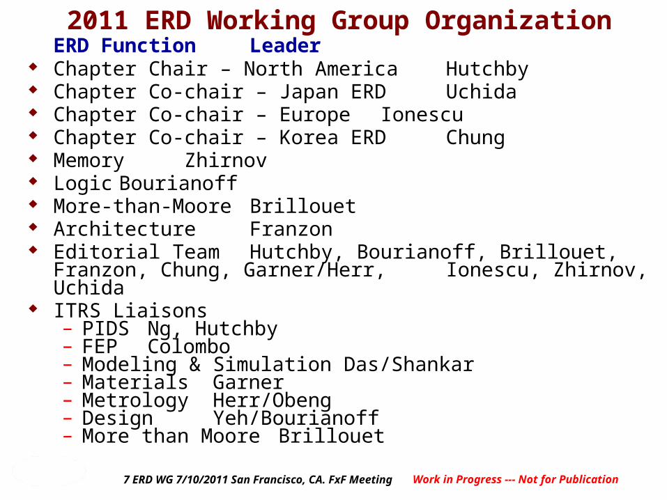
ITRS Liaisons– PIDS Ng, Hutchby– FEP Colombo– Modeling & Simulation Das/Shankar– Materials Garner– Metrology Herr/Obeng– Design Yeh/Bourianoff– More than Moore Brillouet
Work in Progress --- Not for Publication8 ERD WG 7/10/2011 San Francisco, CA. FxF Meeting
2011 ITRS/ERD Major Deliverables and TimelineERD Chapter due August 15, 2011Major Tasks and Time Line Scope, Difficult Challenges, etc. April 30 Outlines for Memory, Logic, MtM, Arch, Mat’l April 30 Technology Requirements Tables July 1 Tables sent to editor August 1 Guiding Principles Section April 30 Draft Text Completed
Memory, Logic, MtM, Architecture, Material June 1 Benchmarking and Critical Review July 1 Chapter Completed Aug. 15 Chapter Frozen Sept. 15
Major Face-to-Face Meetings in 2011 ITRS/ERD Meeting Berlin, Germany April 10 ITRS/ERD Meeting at Semicon West (SF, CA) July 10 ITRS/ERD Meeting near Seoul, Korea Dec. 11
Work in Progress --- Not for Publication9 ERD WG 7/10/2011 San Francisco, CA. FxF Meeting
2011 ITRS/ERD Major Deliverables and Timeline
Work in Progress --- Not for Publication10 ERD WG 7/10/2011 San Francisco, CA. FxF Meeting
# Decisions Made 20111. Memory:
♦Put Vertical MOSFET in the Memory Section.2. Logic:
♦Leave n-channel Ge and InP MOSFETs and p-channel GaSb MOSFETs in ERD/ERM♦The Tunnel FET should remain in the main Logic Tables and Section.♦Nanowire FET stays in ERD/ERM.♦Remove molecular from Logic Section – does not meet criteria♦Add MOTT-FET to the Logic Section♦Remove SET or move SET to the MtM Section♦Keep InP and Ge n-channel and GaSb p-channel MOSFETs in the Logic Section♦Add devices from NRI that meet the selection criteria♦Do not include Vertical MOSFET in Logic; keep/put in Memory Section.♦Change “Collective Spin Wave? to “Spin Wave”.♦Logic Working Group is: Shamik (Nanowires), Adrian (Tunnel FET),??(InP, Ge, GaSb), Jeff Welser (NRI Devices added), Jeff Kitun? ♦ Include the Spin Torque Majority Gate.♦Keep the Atomic Switch in Logic Tables (corrected Feb. 17, 2011)
Work in Progress --- Not for Publication11 ERD WG 7/10/2011 San Francisco, CA. FxF Meeting
Decisions Made 2011
More-than-Moore♦ Architecture issues related to More-than-Moore will be in the MtM Section.♦Consider including items related to on-chip technology integration or “Technology Fusion”
Architectures:♦Add Architectures to the Scope Section♦Sequence of Architecture subsections
o Memoryo Von Neumanno Non Von Neumann
♦Architecture Working Group: Paul Franzon, Tetsua Asai, Matt Marinella, Lou Lome, Sadas Shankar ( Paul and Asai-san will be the writers and all will be commentators.)♦Change Architecture part of Taxonomy Chart. ♦Harvard versus Morphic architecturesNew Highlight Section: Create a new Highlight Section as part of the Critical Assessment Section for :♦Carbon-based Nanoelectronics, and for♦STT-MRAM and Redox RRAMMaterials♦Develop a table of Devices mapped onto materials and their critical property required to demonstrate the key attribute of the device.
Work in Progress --- Not for Publication12 ERD WG 7/10/2011 San Francisco, CA. FxF Meeting
# Action (AI) Items: 2011
1. Add Architectures to the Scope Section Hutchby2. Consider both “Neumann” and “Beyond Neumann” (or
morphic) architectures (Paul Franzon, Tetsua Asai and the Architecture Working Group will explore and develop this approach.
Franzon and Asai
3. Should Storage Class Memory drive a new architecture discussion in the Architecture Section? Explore a definition of SCM
Zhirnov and Schechtman
4. Explore fitting the SET for ADC application in the MtM Section. The SET is still in active research at NTT in Japan.
Brillouet
5. Develop a table of Devices mapped onto materiel and their critical property required to demonstrate the key attribute of the device.
BourianoffGarner and Zhirnov
6. Rename the FeFET to include the Fe-barrier device. Zhirnov7. Send ITRS URL Link to obtain the PPT files of this meeting Hutchby
8. Change “Nanobridge Cantilever” to just “Nanobridge” Zhirnov9. Talk to Jeff Welser regarding which NRI devices meet our
criteria to include them in the ERD Chapter.Bourianoff
10 Consider including items related to on-chip technology integration or “Technology Fusion”
Brillouet
11. Change Architecture part of Taxonomy Chart. Hutchby12, Make the NRI benchmarking methodology available to ERD Welser
13, Prepare a standalone section on benchmarking new devices using new device parameters
WelserBernstein
Work in Progress --- Not for Publication13 ERD WG 7/10/2011 San Francisco, CA. FxF Meeting
Feedback on 2009 ERD Chapter Overall Comments
Excellent overall readability and balance as a summary Appropriate level of detail Scope
Define the terrain covered by performance gains Define “ultimately scaled CMOS” Clarify “new information processing paradigm” Clarify “bulk CMOS”
Difficult Challenges Clarify the term “bridge a knowledge gap” Italicize “This development would provide a significant increase in information …” Give an example of a new application that can be better performed by a new device than
by CMOS. Taxonomy – How useful is this to the reader? Critical Assessment
Some editorial comments Define “functional” Is the term “access resistance” sufficiently general? Comment on “compared to the existing memory technology” Should it say “compared to
existing memory technology scaled to its limit:”? How can we obtain more votes in the Critical Review? Include the OPA score in the left column of ERD 14 and 15.
Work in Progress --- Not for Publication14 ERD WG 7/10/2011 San Francisco, CA. FxF Meeting
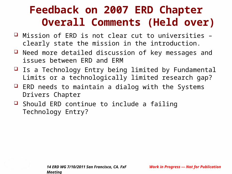
Feedback on 2007 ERD Chapter Overall Comments (Held over)
Mission of ERD is not clear cut to universities – clearly state the mission in the introduction.
Need more detailed discussion of key messages and issues between ERD and ERM
Is a Technology Entry being limited by Fundamental Limits or a technologically limited research gap?
ERD needs to maintain a dialog with the Systems Drivers Chapter Should ERD continue to include a failing Technology Entry?
Work in Progress --- Not for Publication15 ERD WG 7/10/2011 San Francisco, CA. FxF Meeting
Feedback on 2009 ERD ChapterEmerging Research Memory Devices
♦ Transfers Expand the scope by including a new section on the “Select Device”, either a
diode or transistor Expand the scope by including Storage Class Memorysuch as Magnetic
Packet Memory ( Racetrack) Move Nanowire Phase Change Memory to the Memory Transition Table and
recommend its transition to PIDS as a variant of PCM. For the time being, keep the Electronics Effects Memory intact as a category
for further discussion, with the exception of moving Fe Polarization Memory to the FeFET category and devising a new name to distinguish this from the Fe Capacitor Memory
Add a row in the Memory Table to include an indication of a particular memory suitability for SCM
♦ Other comments Include optical memory for More-than-Moore? Need to define (or make a table) a role ( necessary condition) of memory
element as an interconnection. Examples ;o For configurable logic using such as CMOLo For Inference Architecture such as Bayesian inference networks
Work in Progress --- Not for Publication16 ERD WG 7/10/2011 San Francisco, CA. FxF Meeting
Feedback on 2009 ERD ChapterEmerging Research Logic Devices (1/3)
♦ Transfers III-V Alternate Channel Materials to PIDS/FEP and Low Dimensional Materials to PIDS/FEP (keep GNR & CNT FETs) Move Molecular Devices to the Transition Table. Include Band-to-Band Tunneling Device category in Table 1. Move RTD out of Table 2 to Transition Table
♦ Other comments (decisions) Keep the 3 Logic Tables used in 2009 and change “Channel” to “Device”
in the first table. Keep open for more discussion the disposition of vertical MOSFETs –
Decide in Dec. Meeting Put the Tunnel Transistor in the Transition Table for Logic Add a new Section on More-than-Moore focused on Wireless Devices. Move the SET to the new More than Moore Section Move the Negative Capacitive Devices to the Logic Transition Table
Work in Progress --- Not for Publication17 ERD WG 7/10/2011 San Francisco, CA. FxF Meeting
Feedback on 2009 ERD ChapterEmerging Research Logic Devices (2/3)
♦ Other comments (decisions) Include the “Mott FET’ in the Logic Tables. (Call it Electronic Phase Change?) Mention “Excitonic Device” in the Logic Text – put in the Logic Transition
Table? Under Collective Spin Devices include: Spin Wave Device and All Spin Logic The IRC approved the ERD and ERM to publish the results of the Barza
Memory Workshop, but make clear that this is not a selection of a technology Transfer unconventional FET s, Tri-Gate, FinFET, GAA FETs, to PIDS/FEP
♦ Other comments (under discussion) In the Logic Transition Table, the IN/OUT entries for Ge FET, Spin MOSFET,
Collective Spin Devices, Pseudomorphic, and Nanomagnetic Devices should be move into the Comment column to the right. Entries in the IN/OUT column might better be technical in nature.
Work in Progress --- Not for Publication18 ERD WG 7/10/2011 San Francisco, CA. FxF Meeting
Feedback on 2009 ERD ChapterEmerging Research Logic Devices (3/3)
♦ Other comments (under discussion) Introduction of energy efficiency criteria? Important Role of other functionality than digital of beyond CMOS: image
processing, analog, RF, etc. Convergence of beyond CMOS and More than Moore technology
entries? MEMS/NEMS already in chapter. More interaction with emerging architectures needed.
Work in Progress --- Not for Publication ERD WG FxF Meeting 4/10/11 Potsdam, Germany 19
Backup Slides
Work in Progress --- Not for Publication ERD WG FxF Meeting 4/10/11 Potsdam, Germany 20
A Taxonomy for Nano Information Processing Technologies
New
Info
rmat
ion
Proc
essin
g Tec
hnol
ogie
s
Con
vent
iona
l Sca
led
CM
OS
State Variable
Device
Data Representation
Architecture
Material
SETs
Molecular
Spintronics Quantum
Scaled CMOS Ferromagnetic
Quantum
Analog
Digital
Reconfigurable Morphic
Von Neumann
Silicon
Carbon
Ge & III-V mat’ls
Strongly correlated mat’ls
Quantum state
Spin orientationMolecular state
Electric charge Strongly correlated electron state
Phase state
Nanostructured mat’ls
Patterns
Analog
Work in Progress --- Not for Publication21 ERD WG 7/10/2011 San Francisco, CA. FxF Meeting
2009 ITRSEmerging Research Devices
Editorial – Driver Team Meeting
Charter and Scope
George BourianoffMike GarnerJim Hutchby Victor Zhirnov
Santa Clara, CAOctober 13, 2004
Edited December 10, 2006
Work in Progress --- Not for Publication22 ERD WG 7/10/2011 San Francisco, CA. FxF Meeting
Charter of ERD ChapterOn behalf of the 2011 ITRS, develop an Emerging
Research Devices chapter to -- Critically assess new approaches to Information
Processing technology beyond ultimate CMOS Identify most promising approach(es) to Information
Processing technology to be implemented by 2026
To offer substantive guidance to – Global research community Relevant government agencies Technology managers Suppliers
Work in Progress --- Not for Publication23 ERD WG 7/10/2011 San Francisco, CA. FxF Meeting
Scope of ERD Chapter
Integrated emerging research memory, logic and new architecture technologies enabled by supporting -- Materials and process technologies Modeling and simulation Metrologies
Selection of specific technical approaches shall be Guided by fundamental requirements Bounded by ERD’s topic selection criteria
Work in Progress --- Not for Publication24 ERD WG 7/10/2011 San Francisco, CA. FxF Meeting
Scope of ERD Chapter Criteria for Including Technology Entries
Devices and Architectures – Published by 2 or more groups in archival literature and peer
reviewed conferences, or Published extensively by 1 group in archival literature and peer
reviewed conferences Technology Entry (by itself or integrated with CMOS) must
address a major electronics market. Materials and Fabrication Technologies – Materials and processes that address the specific material needs
defined by emerging research device technology entries Supporting disciplines – specify for crosscut TWGs
Metrologies Modeling & simulation
Work in Progress --- Not for Publication25 ERD WG 7/10/2011 San Francisco, CA. FxF Meeting
Decisions for 2009 Chapter
Fig. 4Work in Progress --- Not for Publication8 ERD WG 12/9/07 Washington, DC FxF Meeting
Critical Review – Memory (2011)S
core
cri
teri
a/sc
ale 3
Substantially exceeds the appropriate Baseline Memory Technology scaled to its limit.
* or is compatible with CMOS wafer technology
** or is monolithically integrable with CMOS wafer technology
***or is compatible with CMOS operating temperature
(i.e., Substantially Better than Silicon Baseline Memory Technology)
2
Comparable to the appropriate Baseline Memory Technology scaled to its limit.
* or can be integrated with CMOS architecture with some difficulty
** or is functionally integrable (easily) with CMOS wafer technology
***or requires a modest cooling technology, T > 77K
(i.e., Comparable to Silicon Baseline Memory Technology)
1
Substantially (2î ) inferior to the appropriate Baseline Memory Technology scaled to its limit.
* or can not be integrated with CMOS architecture
** or is not integrable with CMOS wafer technology
***or requires very aggressive cooling technology, T < 77K
(i.e., Substantially Worse than Silicon Baseline Memory Technology)
Work in Progress --- Not for Publication26 ERD WG 7/10/2011 San Francisco, CA. FxF Meeting
Decisions for 2009 Chapter
Fig. 5
9
Beyond CMOS Logic: What to look for?
Required characteristics: Scalability Performance Energy efficiency Gain Operational reliability Room temp. operation
Preferred approach: CMOS process
compatibility CMOS architectural
compatibility
Alternative state variables Spin–electron, nuclear, photon Phase Quantum state Magnetic flux quanta Mechanical deformation Dipole orientation Molecular state
Work in Progress --- Not for Publication27 ERD WG 7/10/2011 San Francisco, CA. FxF Meeting
Decisions for 2009 Chapter
Fig. 6Work in Progress --- Not for Publication11 ERD WG 12/9/07 Washington, DC FxF Meeting
3
Substantially exceeds ultimately scaled CMOS digital information processing technology* or is compatible with CMOS architecture
** or is monolithically integrable with CMOS wafer technology***or is compatible with CMOS operating temperature(i.e., Substantially Better than Silicon CMOS Digital Information ProcessingTechnology)
2
Comparable to ultimately scaled CMOS digital information processing technology* or can be integrated with CMOS architecture with some difficulty** or is functionally integrable (easily) with CMOS wafer technology
***or requires a modest cooling technology, T > 77K(i.e., Comparable to Silicon CMOS Digital Information Processing Technology)
1
Substantially (2î ) inferior to ultimately scaled CMOS digital information processingtechnology.* or cannot be integrated with CMOS architecture
** or is not integrable with CMOS wafer technology***or requires very aggressive cooling technology, T < 77K(i.e., Substantially Worse than Silicon CMOS Digital Information ProcessingTechnology)
Critical Review – Logic (2011)Sc
ore
crit
eria
/sca
le
Work in Progress --- Not for Publication28 ERD WG 7/10/2011 San Francisco, CA. FxF Meeting
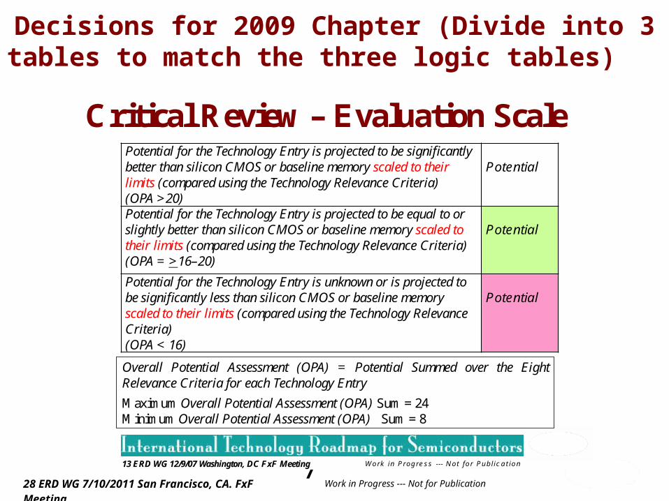
Decisions for 2009 Chapter (Divide into 3 tables to match the three logic tables)
Fig. 7 Work in Progress --- Not for Publication13 ERD WG 12/9/07 Washington, DC FxF Meeting
Critical Review – Evaluation Scale
Overall Potential Assessment (OPA) = Potential Summed over the EightRelevance Criteria for each Technology Entry
Maximum Overall Potential Assessment (OPA) Sum = 24Minimum Overall Potential Assessment (OPA) Sum = 8
Potential for the Technology Entry is projected to be significantly better than silicon CMOS or baseline memory scaled to their limits (compared using the Technology Relevance Criteria) (OPA >20)
Potential
Potential for the Technology Entry is projected to be equal to or slightly better than silicon CMOS or baseline memory scaled to their limits (compared using the Technology Relevance Criteria)(OPA = >16–20)
Potential
Potential for the Technology Entry is unknown or is projected to be significantly less than silicon CMOS or baseline memory scaled to their limits (compared using the Technology Relevance Criteria)(OPA < 16)
Potential
Work in Progress --- Not for Publication29 ERD WG 7/10/2011 San Francisco, CA. FxF Meeting
Work in Progress --- Not for Publication30 ERD WG 7/10/2011 San Francisco, CA. FxF Meeting
“Guiding Principles” Computational state variable(s) other than solely electron charge. These
include spin, phase, multipole orientation, mechanical position, polarity, orbital symmetry, magnetic flux quanta, molecular configuration and other quantum states.
Non-thermal equilibrium systems to reduce the perturbations of the stored information energy by thermal interactions with the environment (e.g., systems that perform all processing functions in a time short compared to the system’s energy relaxation time to improve thermal noise immunity).
Nanoscale thermal management. This might be accomplished by manipulating lattice phonons for constructive energy transport and heat removal.
Novel information transfer mechanisms. These mechanisms would provide the interconnect function between communicating information processing elements, and input/output.
Alternative Architectures. In this case, architecture is the functional arrangement on a single chip of interconnected devices that includes embedded computational components. These architectures should utilize, for special purposes, novel devices other than CMOS to perform unique functions.
Sub-lithographic manufacturing process (e.g., directed self-assembly of complex structures composed of nanoscale building blocks) The approaches should address essential non-regular, hierarchically organized structures, be tied to specific device ideas, and be consistent with high volume manufacturing processes.


![ITRS Winter Conference 2008 Seoul, Korea 1 Work in Progress: Not for Distribution 2008 ITRS Emerging Research Materials [ERM] December 6-9, 2008 Michael.](https://static.documents.pub/doc/80x56/56649e7b5503460f94b7cde6/itrs-winter-conference-2008-seoul-korea-1-work-in-progress-not-for-distribution.jpg)


![ITRS Summer Conference 2012 San Francisco, CA Work in Progress: Not for Distribution 1 2012 ITRS Emerging Research Materials [ERM] July 12, 2012 C. Michael.](https://static.documents.pub/doc/80x56/5514983e550346ea6e8b558b/itrs-summer-conference-2012-san-francisco-ca-work-in-progress-not-for-distribution-1-2012-itrs-emerging-research-materials-erm-july-12-2012-c-michael.jpg)

![ITRS Winter Conference 2010 Makuhari, Japan Work in Progress: Not for Distribution 2010 ITRS Emerging Research Materials [ERM] December 3, 2010 Michael.](https://static.documents.pub/doc/80x56/55149829550346b2598b56b0/itrs-winter-conference-2010-makuhari-japan-work-in-progress-not-for-distribution-2010-itrs-emerging-research-materials-erm-december-3-2010-michael.jpg)

![ITRS Winter Conference 2012 Hsinchu, Taiwan Work in Progress: Not for Distribution 1 2012 ITRS Emerging Research Materials [ERM] December 5, 2012 C. Michael.](https://static.documents.pub/doc/80x56/551496d4550346ea6e8b54cd/itrs-winter-conference-2012-hsinchu-taiwan-work-in-progress-not-for-distribution-1-2012-itrs-emerging-research-materials-erm-december-5-2012-c-michael.jpg)


![ITRS Summer Conference 2011 San Francisco, CA Work in Progress: Not for Distribution 2010 ITRS Emerging Research Materials [ERM] July 13, 2011 C. Michael.](https://static.documents.pub/doc/80x56/55149942550346ea6e8b560f/itrs-summer-conference-2011-san-francisco-ca-work-in-progress-not-for-distribution-2010-itrs-emerging-research-materials-erm-july-13-2011-c-michael.jpg)
![ITRS Winter Conference 2008 Seoul, Korea 1 Work in Progress: Not for Distribution 2008 ITRS Emerging Research Materials [ERM] December 9, 2008 Michael.](https://static.documents.pub/doc/80x56/55149b3b550346b2598b584a/itrs-winter-conference-2008-seoul-korea-1-work-in-progress-not-for-distribution-2008-itrs-emerging-research-materials-erm-december-9-2008-michael.jpg)
