Electromagnetic 23 Compatibility 23.1 Introduction 23/3 23.2 23/3 23.3 23/3 23.4 23/5 23.5 23/6 23.6 23/6 23.7 23/6 23.8 Interfaces 23/7 23.9 23/7 23.10 23/8 23.11 23/8 23.12 23/9 23.13 23/11 23.14 23/11 23.15 Buildings 23/13 23.16 23/13 23.17 23/14 23.18 23/15 A Maddocks Contents Common terms The EMC model EMC requirements Product design Device selection Printed circuit boards Power supplies and power-line filters Signal line filters Enclosure design Interface cable connections Golden rules for effective design for EMC System design Conformity assessment EMC testing and measurements Management plans
Transcript
//integras/b&h/Eer/Final_06-09-02/eerc023
Electromagnetic23 Compatibility
23.1 Introduction 23/3
23.2 23/3
23.3 23/3
23.4 23/5
23.5 23/6
23.6 23/6
23.7 23/6
23.8 Interfaces 23/7
23.9 23/7
23.10 23/8
23.11 23/8
23.12 23/9
23.13 23/11
23.14 23/11
23.15 Buildings 23/13
23.16 23/13
23.17 23/14
23.18 23/15
A Maddocks
Contents
Common terms
The EMC model
EMC requirements
Product design
Device selection
Printed circuit boards
Power supplies and power-line filters
Signal line filters
Enclosure design
Interface cable connections
Golden rules for effective design for EMC
System design
Conformity assessment
EMC testing and measurements
Management plans
//integras/b&h/Eer/Final_06-09-02/eerc023
//integras/b&h/Eer/Final_06-09-02/eerc023
The EMC model 23/3
23.1 Introduction
Electromagnetic Compatibility (EMC) has now become a major consideration on any project involving the design, construction, manufacture and installation of electrical and electronic equipment and systems. Electrical equipment must be designed not only to meet a functional technical performance specification but due consideration must also be given to the interaction the equipment has with the electromagnetic environment in its intended operating location. If the equipment is expected to operate reliably in a steel works, for example, it is imperative that the designers, purchasers, installers and operators are aware of the nature of the electromagnetic environment and the potential for unwanted coupling to the equipment which could cause equipment mis-operation or malfunction. For example, for safety-related equipment, any interference to the operation of the system could have serious consequences. Equally, electromagnetic disturbance generated by the equipment itself could cause interference to radio reception. In the case of domestic radio and TV reception this may adversely affect the quality of reception, but can also block emergency channels and in some cases, e.g. a radio controlled crane, could cause malfunction with potential reliability and safety implications. Generally, both aspects of controlling emis-sions from the equipment and providing adequate immun-ity to the expected electromagnetic disturbances in the intended operating environment are key features of any equipment or system design. The need for emission control has been recognised
for many years and most countries have introduced legal regulations to support the efficient utilisation of the electro magnetic spectrum. This is manifest in the form of require-ments to comply with EMC emission standards in product certification. In some territories such as Europe and Australia, the legal requirements also address immunity aspects. For most manufacturers of good quality equipment this is not an added burden because they are keen to demonstrate to their customers that the equipment will prove to be reliable in the field, and moreover, recognise that any actual incidents of malfunction could be damaging and costly to the business. Fortunately there are advantages for both equipment
suppliers, purchasers and operators in the availability of nationally or internationally approved high quality EMC standards for both emissions and immunity which can be referenced in contractual agreements as well as providing an excellent foundation for the designers of the equipment. Manufacturers and users alike can apply these standards to their mutual advantage, particularly in the planning of major projects. EMC considerations need to be addressed at the outset of
the development. It is well known that the costs of achieving EMC conformity rise almost exponentially with the delay in first considering the requirements. The key issue in addres-sing EMC matters is to adopt a strategic approach where the EMC requirements are recognised and clearly under-stood at the design concept stage, through the product development to in service use, and throughout the lifetime of the equipment.
23.2 Common terms
There are a number of common terms used in the science of EMC. EMC itself can be defined as the ability of equipment to operate satisfactorily within its intended electromagnetic
environment without contributing to the disturbance level in that environment such that radio communication is not adversely affected. Other related terms are RFI and EMI: RFI is radio frequency interference, which is usually defined as interference to radio services in the radio bands, 9 kHz to 300 GHz; EMI, electromagnetic interference, is generally accepted as interference both in the radio frequency bands and in the low frequency region d.c. to 9 kHz. Because of the large ranges of values that are dealt with in
EMC it is customary to express emission limits and system performance in logarithmic ratios, i.e. in dBs. For a voltage or current value, the value in dBs is given by 20 . log10 (ratio) and for power ratios, 10 . log10 (ratio). It is important to recognise that 1 dB in voltage is equivalent to 1 dB in power, although the linear ratios are different, 1.12 and 1.26 respectively. Electric and plane wave fields are expressed in Volts/
metre or dB(mV/m) and magnetic fields are expressed in Amps/metre or dB(mA/m). (1 Amp/metre is equivalent to 1.25 micro Tesla of magnetic induction in free space.)
23.3 The EMC model
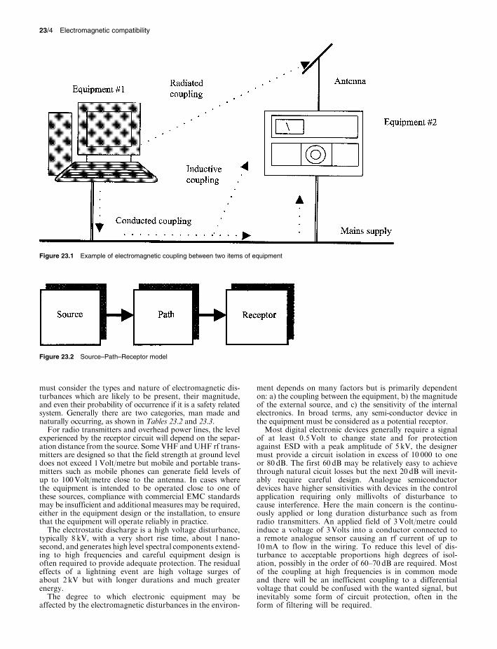
An example of electromagnetic coupling between two items of electrical equipment is illustrated in Figure 23.1. Electrical disturbances generated by equipment #1 may be coupled to equipment #2 by a variety of means: conduction via a common connection to the mains supply, inductive and capacitive coupling between interface and power con-ductors, and by direct radiation. Conducted coupling tends to be the dominant coupling mechanism at lower frequen-cies e.g. below 1 MHz, where conductor impedances are low; capacitive and inductive coupling is more important at higher frequencies where the capacitive impedance between long parallel runs of conductors is relatively low. Radiation coupling dominates at frequencies where the length of the radiating conductor is comparable with a wavelength. For a small computer system, radiation from cables will be promin-ent in the range 30±300 MHz but at higher frequencies, direct radiation from circuit board tracks dominates. Due consideration must be given to these effects in designing and installing equipment and systems. There are many types of coupling that may occur in any
particular application and the key factor for the designer is to recognise and understand the various mechanisms. The simple but effective model source-path-receptor model shown can be applied effectively in dealing with overall requirements (Figure 23.2). For the equipment designer, his product must be con-
sidered both as a source of disturbance and as a potential receptor to disturbances in the intended environment. Emission control is achieved by recognising the potential sources of disturbance within the equipment and the paths by which they may couple to the outside world and cause interference in radio communications. Examples of signifi-cant sources of internally generated electromagnetic distur-bance are given in Table 23.1. Emission control is achieved by effective design, filtering
and suppression measures. The level of control that is normally required is that sufficient for interference free reception of radio communication and radio and TV broadcast services. But the designer of electronic equipment must also
consider his product as a receptor of electromagnetic disturbance in the intended operating environment. For the equipment to work reliably in the field the designer
//integras/b&h/Eer/Final_06-09-02/eerc023
23/4 Electromagnetic compatibility
Figure 23.1 Example of electromagnetic coupling between two items of equipment
Figure 23.2 Source±Path±Receptor model
must consider the types and nature of electromagnetic dis-turbances which are likely to be present, their magnitude, and even their probability of occurrence if it is a safety related system. Generally there are two categories, man made and naturally occurring, as shown in Tables 23.2 and 23.3. For radio transmitters and overhead power lines, the level
experienced by the receptor circuit will depend on the separ-ation distance from the source. Some VHF and UHF rf trans-mitters are designed so that the field strength at ground level does not exceed 1 Volt/metre but mobile and portable trans-mitters such as mobile phones can generate field levels of up to 100 Volt/metre close to the antenna. In cases where the equipment is intended to be operated close to one of these sources, compliance with commercial EMC standards may be insufficient and additional measures may be required, either in the equipment design or the installation, to ensure that the equipment will operate reliably in practice. The electrostatic discharge is a high voltage disturbance,
typically 8 kV, with a very short rise time, about 1 nano-second, and generates high level spectral components extend-ing to high frequencies and careful equipment design is often required to provide adequate protection. The residual effects of a lightning event are high voltage surges of about 2 kV but with longer durations and much greater energy. The degree to which electronic equipment may be
affected by the electromagnetic disturbances in the environ-
ment depends on many factors but is primarily dependent on: a) the coupling between the equipment, b) the magnitude of the external source, and c) the sensitivity of the internal electronics. In broad terms, any semi-conductor device in the equipment must be considered as a potential receptor. Most digital electronic devices generally require a signal
of at least 0.5 Volt to change state and for protection against ESD with a peak amplitude of 5 kV, the designer must provide a circuit isolation in excess of 10 000 to one or 80 dB. The first 60 dB may be relatively easy to achieve through natural cicuit losses but the next 20 dB will inevit-ably require careful design. Analogue semiconductor devices have higher sensitivities with devices in the control application requiring only millivolts of disturbance to cause interference. Here the main concern is the continu-ously applied or long duration disturbance such as from radio transmitters. An applied field of 3 Volt/metre could induce a voltage of 3 Volts into a conductor connected to a remote analogue sensor causing an rf current of up to 10 mA to flow in the wiring. To reduce this level of dis-turbance to acceptable proportions high degrees of isol-ation, possibly in the order of 60±70 dB are required. Most of the coupling at high frequencies is in common mode and there will be an inefficient coupling to a differential voltage that could be confused with the wanted signal, but inevitably some form of circuit protection, often in the form of filtering will be required.
//integras/b&h/Eer/Final_06-09-02/eerc023
EMC requirements 23/5
Table 23.1 Man made sources in equipment
Source or device Electromagnetic disturbance
Digital electronic circuits Harmonics of clock oscillators
Commutator motors High frequency switching transients
Contact devices Showering arc discharges RF oscillators RF fields and voltages Luminaires and Arc discharges Lighting equipment
Switch mode power Harmonics of the switching supplies frequency
Table 23.2 Man made sources in the environment
Source or device Electromagnetic disturbance
Radio transmitters Power distribution
Overhead power lines and railway traction
Rf fields Surges, fast transients, dips and interruptions Magnetic and fields, corona discharges
Table 23.3 Naturally occurring sources in the environment
Source or device Electromagnetic disturbance
Human body electrostatic Electro-static discharges charging
Lightning Fields and power surges
23.4 EMC requirements
The overriding requirement in the supply of equipment to the customer, or in placing the equipment on the market, is to meet the accepted or agreed conformity assessment requirements. For supply of defence equipment for example, the manufacturer will be required to demonstrate that the equipment complies with the EMC specification for the project, such as DEF STAN 59-41 in the UK. The manu-facturer ensures that the equipment is tested to the standard and submits the test report to the project office for approval. In the case of equipment for residential, commer-
cial or industrial application, emission control regulations apply in most territories, and compliance with a relevant EMC standard must be demonstrated. In Europe, Member States have transposed the provisions of the EMC Directive 89/336/EEC into their own legislation. For the vast major-ity of equipment types, the manufacturer can apply a rele-vant standard, which is one harmonised by the Member States and published in the Official Journal of the EC, and make a self declaration of conformity also applying the CE Mark. It should be noted that the CE Mark denotes compliance with all applicable directives which are likely to include at least the Low Voltage Directive in addition to the EMC Directive. Market entry and free circulation of the equipment within the EC is then permitted. The relevant EMC standards are of three types, high
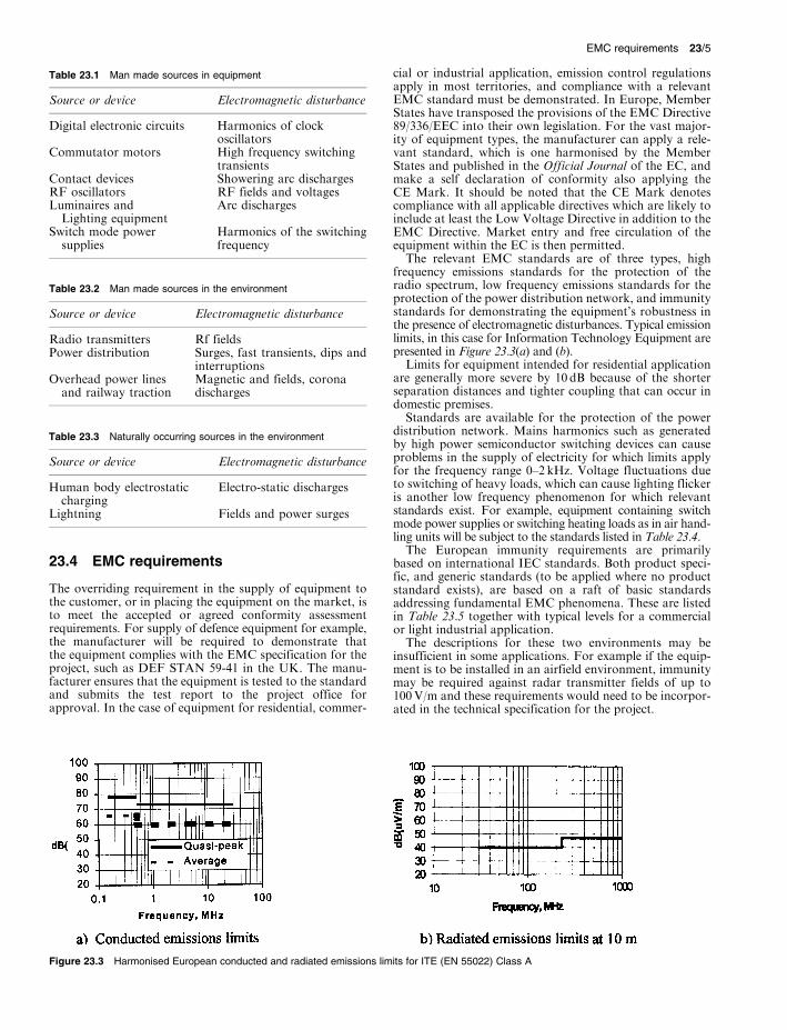
frequency emissions standards for the protection of the radio spectrum, low frequency emissions standards for the protection of the power distribution network, and immunity standards for demonstrating the equipment's robustness in the presence of electromagnetic disturbances. Typical emission limits, in this case for Information Technology Equipment are presented in Figure 23.3(a) and (b). Limits for equipment intended for residential application
are generally more severe by 10 dB because of the shorter separation distances and tighter coupling that can occur in domestic premises. Standards are available for the protection of the power
distribution network. Mains harmonics such as generated by high power semiconductor switching devices can cause problems in the supply of electricity for which limits apply for the frequency range 0±2 kHz. Voltage fluctuations due to switching of heavy loads, which can cause lighting flicker is another low frequency phenomenon for which relevant standards exist. For example, equipment containing switch mode power supplies or switching heating loads as in air hand-ling units will be subject to the standards listed in Table 23.4. The European immunity requirements are primarily
based on international IEC standards. Both product speci-fic, and generic standards (to be applied where no product standard exists), are based on a raft of basic standards addressing fundamental EMC phenomena. These are listed in Table 23.5 together with typical levels for a commercial or light industrial application. The descriptions for these two environments may be
insufficient in some applications. For example if the equip-ment is to be installed in an airfield environment, immunity may be required against radar transmitter fields of up to 100 V/m and these requirements would need to be incorpor-ated in the technical specification for the project.
Figure 23.3 Harmonised European conducted and radiated emissions limits for ITE (EN 55022) Class A
//integras/b&h/Eer/Final_06-09-02/eerc023
23/6 Electromagnetic compatibility
Table 23.4 Low frequency emissions
EMC phenomenon European Basic Standard
Mains harmonics EN 61000-3-2 Voltage fluctuations EN 61000-3-3 (flicker)
23.5 Product design
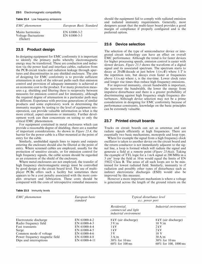
In designing equipment for EMC conformity it is important to identify the primary paths whereby electromagnetic energy may be transferred. These are conduction and induc-tion via the power lead and interface cables, radiation from the PCB circuit tracks and radiation leakage through aper-tures and discontinuities in any shielded enclosure. The aim of designing for EMC conformity is to provide sufficient attenuation in each of the relevant paths such that emission control and provision of adequate immunity is achieved at an economic cost to the product. For many protection meas-ures e.g. shielding and filtering there is reciprocity between measures for emission control and for immunity, although the required degree of attenuation in a particular path may be different. Experience with previous generations of similar products and some exploratory work in determining the immunity margins by testing to the level of equipment mis-operation, can provide valuable information as what is the more critical, aspect emissions or immunity. Further devel-opment work can then concentrate on testing to only the critical EMC phenomenon. For equipment contained in metal enclosures which can
provide a reasonable degree of shielding, there are a number of important considerations. As shown in Figure 23.4, the barrier for the power cable is a filter mounted at the point of entry for the cable. Similarly, unshielded signals lines to inputs and outputs
entering the enclosure should also be filtered at the point of entry. Where screened cables are employed, usually for the protection of sensitive circuits, or for emission control for high frequency signals, the cable screen should be regarded as an extension of the shield of the enclosure. Where metal enclosures are not employed, the transfer of
high frequency electromagnetic energy must be controlled by good design at the circuit board level. The use of multi-player PCBs offers such a facility but sometimes there appears to be a cost penalty associated with the more com-plex structure and fabrication. These costs should be compared with the costs of retrospective remedial measures
Table 23.5 Immunity levels
should the equipment fail to comply with radiated emission and radiated immunity requirements. Generally, most designers accept that the multi-layer board provides a good margin of compliance if properly configured and is the preferred option.
23.6 Device selection
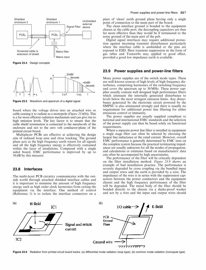
The selection of the type of semiconductor device or inte-grated circuit technology can have an effect on overall EMC performance. Although the trend is for faster devices for higher processing speeds, emission control is easier with slower devices. Figure 23.5 shows the waveform of a digital signal and its associated spectrum. The spectrum starts to decay at 20 dB/decade at just below 1/(�& �(T ) where 1/T is the repetition rate, but decays even faster at frequencies above 1/(�& �( tr) where tr is the rise-time. Lower clock rates and longer rise times thus reduce high frequency emissions. For improved immunity, circuit bandwidth is important,
the narrower the bandwidth, the lower the energy from impulsive disturbance and there is a greater probability of discriminating against high frequency single frequency dis-turbances. Although device selection may not be a prime consideration in designing for EMC conformity because of performance constraints, knowledge on the basic principles can be extremely valuable.
23.7 Printed circuit boards
Tracks on circuit boards can act as antennas and can radiate signals efficiently at high frequencies. There are essentially two basic mechanisms, monopole and loop type. Where for example the signal from a high frequency clock
oscillator is taken to another device on the circuit board and the return conductor is not immediately adjacent to the sig-nal line, a loop is formed which will radiate the signal and generate a field at a remote point (Figure 23.6(a)). Taking the example of TTL logic for a 1 mA signal at 200 MHz in a 3 cm2 loop the field at 10 m would equal the limits of EN 55022 Class B. The areas of all such loops are to be min-imised for lowest radiated field. Similarly, immunity to rf radiation and possibly other types of disturbance such as indirect electrostatic discharges (ESD) would also be improved by this measure. However a more important mechanism is where a voltage
is generated across the length of the ground return on the
EMC phenomenon European basic Typical disturbance level standard a.c. power port
Residential, Industrial environment commercial and light industrial environment
Electrostatic discharge EN 61000-4-2 8 kV (air discharge) 8 kV (air discharge) Radio frequency field EN 61000-4-3 3 V/m 10 V/m Fast transients EN 61000-4-4 1 kV 2 kV Surge EN 61000-4-5 1 kV 2 kV Common mode rf voltage EN 61000-4-6 3 V 10 V Power frequency magnetic field EN 61000-4-8 3 A/m 30 A/m Dips and interruptions EN 61000-4-11 30% for 10 ms 30% for 10 ms
60% for 100 ms 60% for 100, 1000 ms
//integras/b&h/Eer/Final_06-09-02/eerc023
Power supplies and power-line filters 23/7
Shielded Shielded piece of `clean' earth ground plane having only a single enclosure 2 enclosure 1 Unshielded
point of connection to the main part of the board. Signal Filter
Mains filter
Mains input
PCB2PCB2
external device
Screened cable is extension of shield
Figure 23.4 Design concepts
A
20dB/ decade
–40dB/ decade
π 1/πtr 1T tr 1/ T
Figure 23.5 Waveform and spectrum of a digital signal
board where the voltage drives into an attached wire or cable causing it to radiate as a monopole (Figure 23.6(b)). This is a far more efficient radiation mechanism and can give rise to high emission levels. The key factor is to ensure that the cable shield termination is connected to the metalwork of the enclosure and not to the zero volt conductor/plane of the printed circuit board. Multiplayer PCBs are effective at achieving the design
aim of reduced loop area and close tracking. The ground plane acts as the high frequency earth return for all signals and all the high frequency energy is effectively contained within the layer of insulations. Compared with a single sided board, EMC performance is improved by up to 30 dB by this measure.
23.8 Interfaces
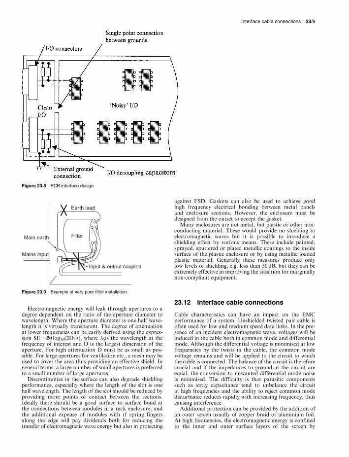
The multi-layer PCB circuitry communicates with the out-side world through attached shielded interface cables and it is important to minimise the amount of high frequency energy such as high order clock harmonics from exiting the equipment via the interface. One method of control (Reference 1) is to isolate the interface connectors on a
The clean interface ground is bonded to the equipment chassis at the cable port; the decoupling capacitors are thus far more effective than they would be if terminated to the noisy ground of the main part of the pcb. Digital signal interfaces may require additional protec-
tion against incoming transient disturbances particularly where the interface cable is unshielded or the pins are exposed to ESD. Here transient suppression in the form of gas tubes and Transorbs may applied to good effect, provided a good low impedance earth is available.
23.9 Power supplies and power-line filters
Many power supplies are of the switch mode types. These are well-known sources of high levels of high frequency dis-turbance, comprising harmonics of the switching frequency and cover the spectrum up to 30 MHz. These power sup-plies usually contain well designed high performance filters which attenuate the internally generated disturbance to levels below the most stringent emission limits. Any distur-bance generated by the electronic circuit powered by the SMPSU is also attenuated strongly and there is usually no requirement for additional power line filtering for either emissions control or immunity. The power supplies are usually supplied compliant to
national and international EMC standards and the selection of the power supply can then be based solely on functional requirements. Where a separate power line filter is installed in equipment
a single stage filter can often be selected by choosing the largest line inductance at the rated current. However, overall EMC performance is generally determined by EMC tests on the complete system because the practical terminating imped-ances are usually unknown for all the modes of propagation, and calculations or estimates based on manufacturers' data can often be accompanied by high uncertainties. The performance of the filter will be critically dependent
on the filter installation method. Figure 23.9 shows an example of bad installation practice. The performance is severely degraded by cross coupling via the bundled input and output wires and the earth is provided by a wire. The impedance of the wire is in series with the suppression cap-acitors between the power conductors and the equipment chassis and the high frequency performance of the filter will be degraded. The metal body of the filter should be bonded directly to the chassis via a shake-proof washer and not by a wire and the input and output wires should
Figure 23.6 Radiation from printed circuit board tracks: (a) differential mode radiation (loop type); (b) common mode radiation (monopole type)
//integras/b&h/Eer/Final_06-09-02/eerc023
23/8 Electromagnetic compatibility
Copper circuit
Insulation
plate (DV)
material
Circuit component
Figure 23.7 Ground plane board
be separated and aligned 180 degrees in opposition to one another.
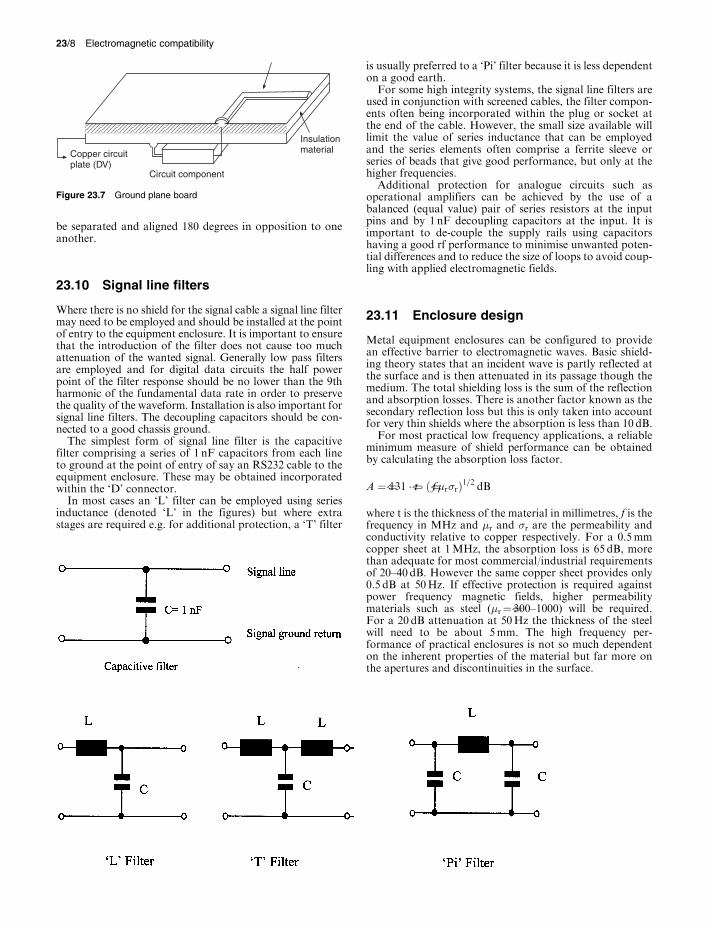
23.10 Signal line filters
Where there is no shield for the signal cable a signal line filter may need to be employed and should be installed at the point of entry to the equipment enclosure. It is important to ensure that the introduction of the filter does not cause too much attenuation of the wanted signal. Generally low pass filters are employed and for digital data circuits the half power point of the filter response should be no lower than the 9th harmonic of the fundamental data rate in order to preserve the quality of the waveform. Installation is also important for signal line filters. The decoupling capacitors should be con-nected to a good chassis ground. The simplest form of signal line filter is the capacitive
filter comprising a series of 1 nF capacitors from each line to ground at the point of entry of say an RS232 cable to the equipment enclosure. These may be obtained incorporated within the `D' connector. In most cases an `L' filter can be employed using series
inductance (denoted `L' in the figures) but where extra stages are required e.g. for additional protection, a `T' filter
is usually preferred to a `Pi' filter because it is less dependent on a good earth. For some high integrity systems, the signal line filters are
used in conjunction with screened cables, the filter compon-ents often being incorporated within the plug or socket at the end of the cable. However, the small size available will limit the value of series inductance that can be employed and the series elements often comprise a ferrite sleeve or series of beads that give good performance, but only at the higher frequencies. Additional protection for analogue circuits such as
operational amplifiers can be achieved by the use of a balanced (equal value) pair of series resistors at the input pins and by 1 nF decoupling capacitors at the input. It is important to de-couple the supply rails using capacitors having a good rf performance to minimise unwanted poten-tial differences and to reduce the size of loops to avoid coup-ling with applied electromagnetic fields.
23.11 Enclosure design
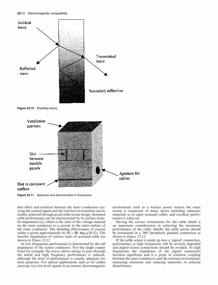
Metal equipment enclosures can be configured to provide an effective barrier to electromagnetic waves. Basic shield-ing theory states that an incident wave is partly reflected at the surface and is then attenuated in its passage though the medium. The total shielding loss is the sum of the reflection and absorption losses. There is another factor known as the secondary reflection loss but this is only taken into account for very thin shields where the absorption is less than 10 dB. For most practical low frequency applications, a reliable
minimum measure of shield performance can be obtained by calculating the absorption loss factor.
A �( 131 �( t � �( f �r�r�1=2 dB
where t is the thickness of the material in millimetres, f is the frequency in MHz and �r and �r are the permeability and conductivity relative to copper respectively. For a 0.5 mm copper sheet at 1 MHz, the absorption loss is 65 dB, more than adequate for most commercial/industrial requirements of 20±40 dB. However the same copper sheet provides only 0.5 dB at 50 Hz. If effective protection is required against power frequency magnetic fields, higher permeability materials such as steel (�r �( 300±1000) will be required. For a 20 dB attenuation at 50 Hz the thickness of the steel will need to be about 5 mm. The high frequency per-formance of practical enclosures is not so much dependent on the inherent properties of the material but far more on the apertures and discontinuities in the surface.
//integras/b&h/Eer/Final_06-09-02/eerc023
Figure 23.8 PCB interface design
Mains input
Input & output coupled
FilterMain earth
Earth lead
Figure 23.9 Example of very poor filter installation
Electromagnetic energy will leak through apertures to a degree dependent on the ratio of the aperture diameter to wavelength. Where the aperture diameter is one half wave-length it is virtually transparent. The degree of attenuation at lower frequencies can be easily derived using the expres-sion SE �( 20 log10(2D/�), where �& is the wavelength at the frequency of interest and D is the largest dimension of the aperture. For high attenuation D must be as small as pos-sible. For large apertures for ventilation etc., a mesh may be used to cover the area thus providing an effective shield. In general terms, a large number of small apertures is preferred to a small number of large apertures. Discontinuities in the surface can also degrade shielding
performance, especially where the length of the slot is one half wavelength. The length of the slot should be reduced by providing more points of contact between the sections. Ideally there should be a good surface to surface bond at the connections between modules in a rack enclosure, and the additional expense of modules with rf spring fingers along the edge will pay dividends both for reducing the transfer of electromagnetic wave energy but also in protecting
Interface cable connections 23/9
against ESD. Gaskets can also be used to achieve good high frequency electrical bonding between metal panels and enclosure sections. However, the enclosure must be designed from the outset to accept the gasket. Many enclosures are not metal, but plastic or other non-
conducting material. These would provide no shielding to electromagnetic waves but it is possible to introduce a shielding effect by various means. These include painted, sprayed, sputtered or plated metallic coatings to the inside surface of the plastic enclosure or by using metallic loaded plastic material. Generally these measures produce only low levels of shielding, e.g. less than 30 dB, but they can be extremely effective in improving the situation for marginally non-compliant equipment.
23.12 Interface cable connections
Cable characteristics can have an impact on the EMC performance of a system. Unshielded twisted pair cable is often used for low and medium speed data links. In the pre-sence of an incident electromagnetic wave, voltages will be induced in the cable both in common mode and differential mode. Although the differential voltage is minimised at low frequencies by the twists in the cable, the common mode voltage remains and will be applied to the circuit to which the cable is connected. The balance of the circuit is therefore crucial and if the impedances to ground at the circuit are equal, the conversion to unwanted differential mode noise is minimised. The difficulty is that parasitic components such as stray capacitance tend to unbalance the circuit at high frequencies and the ability to reject common mode disturbance reduces rapidly with increasing frequency, thus causing interference. Additional protection can be provided by the addition of
an outer screen usually of copper braid or aluminium foil. At high frequencies, the electromagnetic energy is confined to the inner and outer surface layers of the screen by
//integras/b&h/Eer/Final_06-09-02/eerc023
23/10 Electromagnetic compatibility
Figure 23.10 Shielding theory
Figure 23.11 Apertures and discontinuities in Enclosures
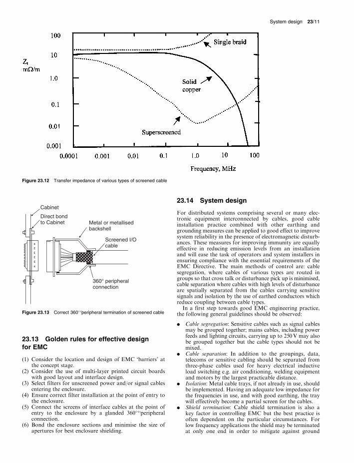
skin effect and isolation between the inner conductors car-rying the wanted signal and the external environment can be readily achieved through good cable screen design. Screened cable performance can be characterised by its surface trans-fer impedance (Zt) which is the ratio of the voltage induced on the inner conductor to a current in the outer surface of the outer conductor. The shielding effectiveness of coaxial cables is given approximately by SE �( 20 �( log10(50/Zt). The transfer impedances of various types of screened cable are shown in Figure 23.12. At low frequencies performance is determined by the self
impedance of the screen conductor. For the single copper braid for example, the weave allows energy to pass through the shield and high frequency performance is reduced, although the level of performance is usually adequate for most purposes. For special applications such as for cables carrying very low level signals in an intense electromagnetic
environment such as a nuclear power station the outer screen is composed of many layers including inductive materials as in super screened cables, and excellent perfor-mance is achieved. Having the correct termination for the cable shield is
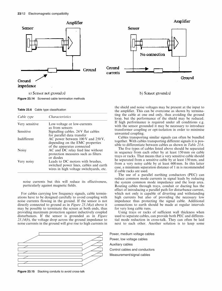
an important consideration in achieving the maximum performance of the cable. Ideally the cable screen should be terminated in a 360�( peripheral glanded connection as shown in Figure 23.13. If the cable screen is made up into a `pigtail' connection,
performance at high frequencies will be severely degraded and pigtail screen connections should be avoided. At high frequencies the impedance of the pigtail connection becomes significant and is a point of common coupling between the inner conductors and the external environment, increasing emissions and reducing immunity to external disturbances.
//integras/b&h/Eer/Final_06-09-02/eerc023
Figure 23.12 Transfer impedance of various types of screened cable
Cabinet
Direct bond to Cabinet Metal or metallised
Screened I/O cable
backshell
360° peripheral connection
Figure 23.13 Correct 360�( peripheral termination of screened cable
23.13 Golden rules for effective design for EMC
(1) Consider the location and design of EMC `barriers' at the concept stage.
(2) Consider the use of multi-layer printed circuit boards with good layout and interface design.
(3) Select filters for unscreened power and/or signal cables entering the enclosure.
(4) Ensure correct filter installation at the point of entry to the enclosure.
(5) Connect the screens of interface cables at the point of entry to the enclosure by a glanded 360�( peripheral connection.
(6) Bond the enclosure sections and minimise the size of apertures for best enclosure shielding.
System design 23/11
23.14 System design
For distributed systems comprising several or many elec-tronic equipment interconnected by cables, good cable installation practice combined with other earthing and grounding measures can be applied to good effect to improve system reliability in the presence of electromagnetic disturb-ances. These measures for improving immunity are equally effective in reducing emission levels from an installation and will ease the task of operators and system installers in ensuring compliance with the essential requirements of the EMC Directive. The main methods of control are: cable segregation, where cables of various types are routed in groups so that cross talk or disturbance pick up is minimised, cable separation where cables with high levels of disturbance are spatially separated from the cables carrying sensitive signals and isolation by the use of earthed conductors which reduce coupling between cable types. In a first step towards good EMC engineering practice,
the following general guidelines should be observed:
. Cable segregation: Sensitive cables such as signal cables may be grouped together; mains cables, including power feeds and lighting circuits, carrying up to 250 V may also be grouped together but the cable types should not be mixed.
. Cable separation: In addition to the groupings, data, telecoms or sensitive cabling should be separated from three-phase cables used for heavy electrical inductive load switching e.g. air conditioning, welding equipment and motors by the largest practicable distance.
. Isolation: Metal cable trays, if not already in use, should be implemented. Having an adequate low impedance for the frequencies in use, and with good earthing, the tray will effectively become a partial screen for the cables.
. Shield termination: Cable shield termination is also a key factor in controlling EMC but the best practice is often dependent on the particular circumstances. For low frequency applications the shield may be terminated at only one end in order to mitigate against ground
//integras/b&h/Eer/Final_06-09-02/eerc023
23/12 Electromagnetic compatibility
Figure 23.14 Screened cable termination methods
Table 23.6 Cable type classification
Cable type Characteristics
Very sensitive Low-voltage or low-currents as from sensors
Sensitive Signalling cables. 24 V flat cables for parallel data transfer
Indifferent AC power between 100 V and 250 V, depending on the EMC properties of the apparatus connected
Noisy AC and DC relay feed line without protection measures such as filters or diodes
Very noisy Leads to DC motors with brushes, switched power lines, cables and earth wires in high voltage switchyards, etc.
noise currents but this will reduce its effectiveness, particularly against magnetic fields.
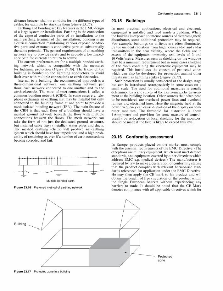
For cables carrying low frequency signals, cable termin-ations have to be designed carefully to avoid coupling with noise currents flowing in the ground. If the sensor is not directly connected to ground as in Figure 23.14(a) above it may be possible to terminate the screen at both ends, thus providing maximum protection against inductively coupled disturbances. If the sensor is grounded as in Figure 23.14(b), the voltage drop across the ground impedance to noise currents in the ground will give rise to high currents in
the shield and noise voltages may be present at the input to the amplifier. This can be overcome as shown by termina-ting the cable at one end only, thus avoiding the ground loop, but the performance of the shield may be reduced. If high performance is required under all conditions e.g. with the sensor grounded it may be necessary to introduce transformer coupling or opt-isolation in order to minimise unwanted coupling. Cables transporting similar signals can often be bundled
together. With cables transporting different signals it is pos-sible to differentiate between cables as shown in Table 23.6. The five types of cables listed above should be separated
in sequence from each other by at least 150 mm on cable trays or racks. That means that a very sensitive cable should he separated from a sensitive cable by at least 150 mm, and from a very noisy cable by at least 600 mm. In this latter case, a minimum separation distance of 1 m is recommended if cable racks are used. The use of a parallel earthing conductors (PEC) can
reduce common mode currents in signal leads by reducing the system common mode impedance and the loop area. Routing cables through trays, conduit or ducting has the effect of introducing a parallel path for disturbance current, which not only is capable of diverting and withstanding high currents but also of providing the necessary low impedance thus protecting the signal cable. Additional connections to earth should be made at regular intervals for very long cable runs. Using trays or racks of sufficient wall thickness when
used to separate cables, can provide both PEC and differen-tial mode reduction in cross-talk. They can often be laid next to each other. Another solution is to keep some
Power, medium voltage cables
Power, low voltage cables
Auxiliary cables
Control cables and conductors
Measurement/signal cables
Figure 23.15 Stacking conduits to avoid cross-talk
//integras/b&h/Eer/Final_06-09-02/eerc023
Conformity assessment 23/13
distance between shallow conduits for the different types of cables, for example by stacking them (Figure 23.15). Earthing and bonding are key features in the EMC design
of a large system or installation. Earthing is the connection of the exposed conductive parts of an installation to the main earthing terminal of that installation; bonding is an electrical connection maintaining various exposed conduc-tive parts and extraneous conductive parts at substantially the same potential. The general requirements of an earthing network are to provide safety and to provide a low imped-ance path for currents to return to source. The current preferences are for a multiple bonded earth-
ing network which is compatible with the measures for lightning protection (Figure 23.16). The frame of the building is bonded to the lightning conductors to avoid flash-over with multiple connections to earth electrodes. Internal to a building, the recommended approach is a
three-dimensional network, one earthing network per floor, each network connected to one another and to the earth electrode. The mass of inter-connections is called a common bonding network (CBN). In some cases e.g. tele-phone exchanges an earthing mat may be installed but only connected to the building frame at one point to provide a mesh isolated bonding network (IBN). The main feature of the CBN is that each floor of a building should have a meshed ground network beneath the floor with multiple connections between the floors. The mesh network can take the form of not just the dedicated ground structure, but installed cable trays (metallic), water pipes and ducts. The meshed earthing scheme will produce an earthing system which should have low impedance, and a high prob-ability of remaining so, even if a number of earth connections become corroded and fail.
Multiple bonded earth
Figure 23.16 Preferred method of earthing network
Building
23.15 Buildings
In most practical applications, electrical and electronic equipment is installed and used inside a building. Where the building is exposed to intense sources of electromagnetic disturbance, some additional protection may be required. For example, buildings on airfields are often illuminated by the incident radiation from high power radio and radar transmitters in the near vicinity, where the fields are in excess of the equipment immunity test levels of 3 and 10 Volts/metre. Measures such as shielding on the windows may be a minimum requirement but in some cases shielding of the room containing the electronic equipment may be required. This introduces the concept of protected zones which can also be developed for protection against other threats such as lightning strikes (Figure 23.17). Such protection is usually considered at the design stage
but can be introduced retrospectively in some cases on a small scale. The need for additional measures is usually determined by a site survey of the electromagnetic environ-ment at the building location. Other sources that often need to be considered are overhead power lines and overhead railway a.c. electrified lines. Here the magnetic field at the power frequency can cause distortion of the display on com-puter monitors. The threshold for distortion is about 1 Amp/metre and provision for some measure of control, usually by re-location or local shielding for the monitors, should be made if the field is likely to exceed this level.
23.16 Conformity assessment
In Europe, products placed on the market must comply with the essential requirements of the EMC Directive. (The exceptions are military equipment, which must meet defence standards, and equipment covered by other directives which address EMC e.g. medical devices.) The manufacturer is required by law to make a declaration of conformity stating that the product complies with relevant harmonised stan-dards referenced for application under the EMC Directive. He may then apply the CE mark to his product and will obtain the benefit of free circulation of the product within the Single European Market without experiencing any barriers to trade. It should be noted that the CE Mark denotes compliance with all applicable directives which for
Protected zone
Figure 23.17 Protected zone in a building
//integras/b&h/Eer/Final_06-09-02/eerc023
23/14 Electromagnetic compatibility
Table 23.7 European directives and EMC standards
Product Directive EMC Standards
Household equipment Maritime navigation equipment
Lighting equipment Information Technology Equipment
Railway Equipment Low Voltage Switchgear Radio and TV receivers Radio and radio-telecommunications equipment Medical equipment
Medical Devices Directive 93/42 EEC Automotive EMC Directive 95/54/EEC
EN 55014-1 and ±2 EN 60945
EN 55015 and EN 61547 EN 55022 and EN 55024
prEN 50121 parts 2±5 EN 60947 EN 55013 and EN 55020 Applicable TBR, EN or ETS standards EN 60601-1-2
The directive contains the technical requirements
most products, will also include the electrical safety require-ments of the Low Voltage Directive 73/23/EEC. For finished products, complex components and systems,
the manufacturer has the option of either applying appro-priate harmonised EMC standards i.e. those approved by the European Commission or can prepare a Technical Construction File where the harmonised standards are not available or are not applied in full. Generally most manu-facturers apply the harmonised standards as the most cost-effective route and this usually means that the product must be tested to EMC standards to determine compliance. Table 23.7 presents examples of the requirements for
common types of electrical and electronic equipment. It is the responsibility of the manufacturer to determine
which directives apply to his product but information is usually generally available from standards bodies such as the BSI, from EMC test laboratories and Competent Authorities such as the UK's Department of Trade and Industry. The European assessment requirements for fixed installa-
tions are somewhat different. The installation may comprise compliant (CE marked) equipment and/or non-compliant equipment. The installation must meet the `essential requirement' of the EMC Directive, i.e. not to cause interfer-ence and not to be affected by electromagnetic disturbance. There is no necessity for declaring compliance nor for CE marking. However the installation designer should ensure that the equipment is installed according to good engineer-ing practice and is advised to maintain a file containing a description of the EMC measures taken, together with any test data etc. This file should be available for inspection by the authorities if challenged at some later date. The key issue is the acceptance by the designer or operator of non-compliant equipment. This is permissible but becomes the responsibility of the operator if interference results and therefore the operator should ensure that this equipment is compatible with its environment either by imposing some contractual requirements for EMC characterisation on the supplier or by in-situ confidence testing.
23.17 EMC testing and measurements
For the vast majority of electrical and electronic equipment, compliance with the relevant technical specification is achieved by testing to EMC standards. Emissions measure-
ments can comprise two types, a) tests for low frequency phenomena such as power frequency harmonics and voltage fluctuations to protect the power distribution network, and b) high frequency emissions to protect the radio spectrum. For commercial and industrial products, high frequency emission measurements are normally made over the fre-quency range 150 kHz to 1 GHz but some standards call for measurements down to 9 kHz. It should be noted that it is becoming increasingly necessary to measure emissions above 1 GHz to protect cellular and other radio systems. The low frequency phenomena are usually measured with
proprietary test instrumentation dedicated for that purpose comprising a harmonics analyser and flicker meter. Most high frequency tests comprise measurements of conducted disturbance over the frequency range 150 kHz to 30 MHz and radiated disturbance at higher frequencies, 30 MHz to 1000 MHz. The different test methods effectively reflect the propagation mechanisms that dominate in practice. Conducted disturbance measurements on the mains
power input comprise a measurement of rf voltage across a passive network (50 uH/50 ohms) having an input imped-ance representative of the rf impedance of the mains at high frequencies. The voltage is measured using a calibrated EMC measuring receiver or spectrum analyser. Most mod-ern instrumentation systems are computer controlled for maximum efficiency. Radiated measurements are performed on a test range
meeting particular requirements for path loss, or in a facil-ity giving results which can be correlated to those on the test range. The standard test range comprises on open area site which is flat and free from reflecting objects and typically having the dimensions shown in Figure 23.18. A significant proportion of the area should be covered by a conducting ground plane in order to achieve the site attenuation cali-bration requirements. Shielded enclosures lined with radio-wave absorbing
material or ferrite tiles on all internal sides except the floor can be constructed to achieve site attenuation performance characteristics comparable with an open area test site. Due to cost limitations, most chambers are built to accommo-date a 3 metre range and some additional calibration work may be required to relate the results to the 10 metre range, particularly for physically large items of equipment. Measurements of field strength are made using a receiver
or spectrum analyser and a calibrated antenna situated at a fixed distance from the equipment under test. A key factor
//integras/b&h/Eer/Final_06-09-02/eerc023
Management plans 23/15
Figure 23.18 Dimensions of the CISPR open area test for radiated emissions
Table 23.8 Test equipment
Test
ESD Fast transients
Surges Dips and interruptions Rf fields
Rf voltages
Equipment
ESD Gun Transient generator and coupling clamp Surge generator Dips generator Signal generator, power amplifiers, antennas Signal generator, power amplifiers, coupling networks
in emissions measurements is to configure and operate the product in a manner which is both representative of practical use, yet maximises the emissions from the product. For products and small systems which contain cables some pre-testing is often required to determine the optimum con-figuration for test, particularly for radiated emissions tests. Immunity tests are performed by subjecting the equip-
ment to electromagnetic disturbances of the type and maximum level that the product is likely to encounter in its intended operating environment. For many of the tests, specialised test instrumentation is required, providing the well-defined disturbance characteristics described in the standards. The instrumentation is commonly available from a number of specialist suppliers and the tests which involve the direct application of disturbance voltages are relatively straightforward. The facilities for subjecting the product to disturbance
fields are more complex and costly. The rf field immunity test is performed inside a shielded room lined with radio-wave absorbing material or ferrite tiles and the costs of purchasing and installing the facility are often quite high. The test method requires that the test volume is pre-calibrated to achieve the desired test level. There is an additional field uniformity requirement for the maximum level of field over 75% of a 1.5 m square area to be no greater than twice the required test level. Rf power over the frequency range 80±1000 MHz is fed to a dedicated radiating antenna in the room from a signal generator and high power amplifier. The system is usually computer controlled to achieve the calibrated level in an efficient and reproducible manner. To simulate coupling with rf fields at frequencies below
80 MHz, a common mode voltage test is applied to the cables attached to the product, i.e. the mains leads and signal and interface cables using coupling/decoupling networks
(CDNs). The measurements are usually made inside the shielded enclosure for convenience and to avoid causing interference to radio services. Immunity to power frequency magnetic fields is performed
by setting up current flow in a loop around the product or preferably by placing the product within the confines of a Helmholtz coil. In immunity testing, the configuration and operating
conditions of the equipment under test can be very import-ant. These conditions are usually specified in the EMC standard applicable to the product but in the absence of specific information the test engineer must attempt to adjust the conditions for maximum sensitivity to the applied dis-turbance. This can be difficult because immunity testing does not give a resultant variable, only an attribute of com-pliance or non-compliance, and care is required to follow the specific instructions of the standard and the advice and guidance of the manufacturer. Monitoring of the product's performance should be performed in a non-invasive method that does not influence the coupling of the applied distur-bance. In addition the criteria for assessing the product's performance need to be clearly established prior to testing. For example for an analogue instrument such as a tempera-ture sensor, the margin of acceptable error, say 1%, needs to be stated in the User Manual.
23.18 Management plans
For all product, system or installation developments, com-pliance with EMC requirements can be made much easier by the adoption and adherence to an EMC management plan. This would probably be integrated within a broader conformity assessment programme which would include
Table 23.9. Product development process
Product development EMC input stage
Design Concept Apply EMC control principles Design Process EMC design measures Prototype Pre-compliance EMC tests Production Prototype EMC certification Production Conformity in production tests Upgrades/modifications EMC re-assessment
//integras/b&h/Eer/Final_06-09-02/eerc023
23/16 Electromagnetic compatibility
safety and other approvals. The plan would be prepared at the inception of the product development with an intention of achieving complete compliance at the lowest cost and in the shortest timeframe both at the initial certification stage and also through the lifetime of the product. The plan would include Control Plans which would specify the intended operating electromagnetic environment, any particular EMC elements in the Technical Specification, a Compatibility Matrix to identify couplings with other systems, EMC Test Plans, and applicable codes of practice to aid the design team. Table 23.9 lists the EMC inputs required at the various stages of a product development. Procedures can be set up for regular EMC design
reviews and formal acceptance of supplied sub-assemblies or equipment from sub-contractors. In some cases, particularly for large systems and installations, it may be necessary to establish procedures for dealing with concession requests and dispensations where supplied items are non-compliant.
References
1 PAUL, C. R., Introduction to Electromagnetic Compatibility, John Wiley and Sons Inc (1992)
2 GREEN, M., Optimised and Superscreened cables, Raychem Ltd
3 Design for EMC. ERA Report 90-006, ERA Technology Ltd (1990)
4 DEGAUQUE, P. and HAMELIN, J., Electromagnetic Compatibility, Oxford University Press (1993)
5 OTT, H. W., Noise Reduction Techniques in Electronic Systems, John Wiley Interscience, NY (1988)
6 GOEDBLOED, J. J., Electromagnetic Compatibility, Prentice Hall (1992)
7 Cabling Installations: User Friendly Guide, ERA Report No 98-0668
8 Information TechnologyÐCabling Installation, Part 2 Installation Planning and Practices inside Buildings, prEN 50174-2 June 1998