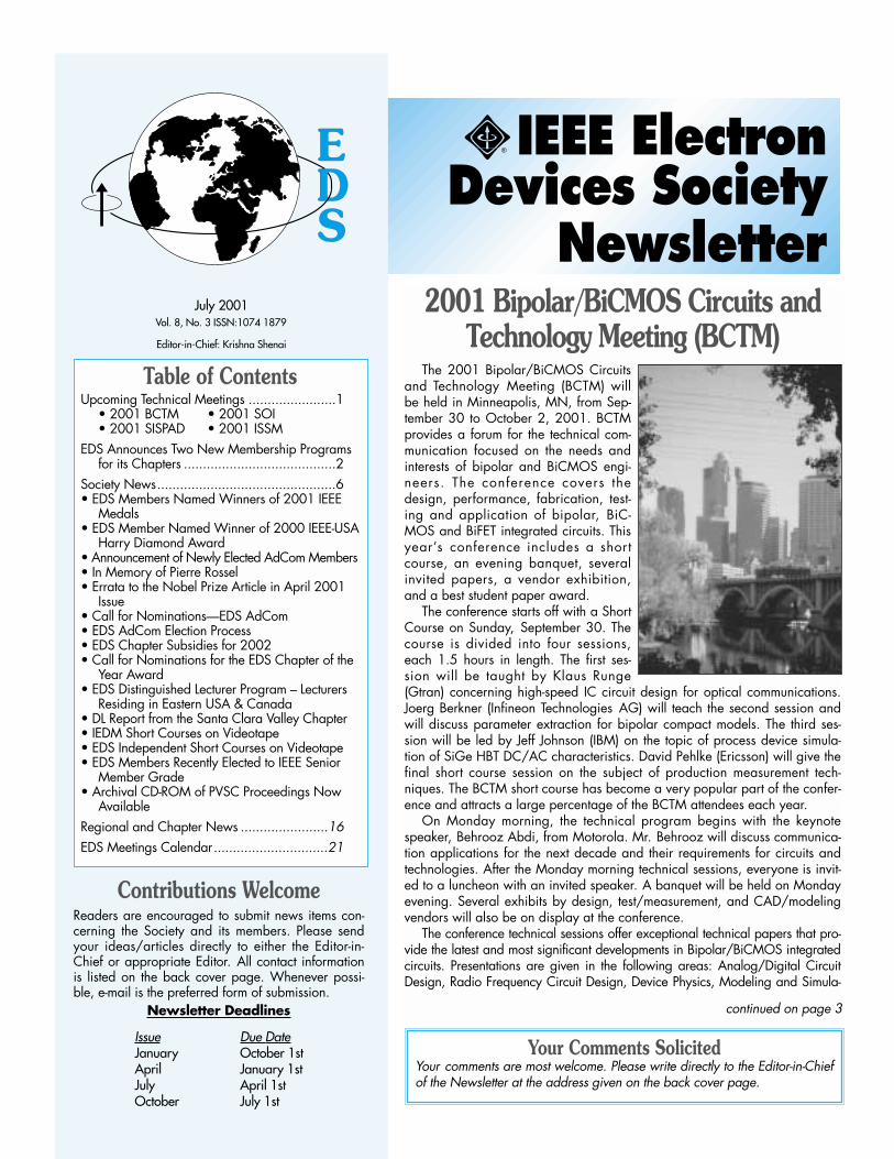
The 2001 Bipolar/BiCMOS Circuits and Technology Meeting (BCTM) will be held in Minneapolis, MN, from Sep- tember 30 to October 2, 2001. BCTM provides a forum for the technical com- munication focused on the needs and interests of bipolar and BiCMOS engi- neers. The conference covers the design, performance, fabrication, test- ing and application of bipolar, BiC- MOS and BiFET integrated circuits. This year’s conference includes a short course, an evening banquet, several invited papers, a vendor exhibition, and a best student paper award. The conference starts off with a Short Course on Sunday, September 30. The course is divided into four sessions, each 1.5 hours in length. The first ses- sion will be taught by Klaus Runge (Gtran) concerning high-speed IC circuit design for optical communications. Joerg Berkner (Infineon Technologies AG) will teach the second session and will discuss parameter extraction for bipolar compact models. The third ses- sion will be led by Jeff Johnson (IBM) on the topic of process device simula- tion of SiGe HBT DC/AC characteristics. David Pehlke (Ericsson) will give the final short course session on the subject of production measurement tech- niques. The BCTM short course has become a very popular part of the confer- ence and attracts a large percentage of the BCTM attendees each year. On Monday morning, the technical program begins with the keynote speaker, Behrooz Abdi, from Motorola. Mr. Behrooz will discuss communica- tion applications for the next decade and their requirements for circuits and technologies. After the Monday morning technical sessions, everyone is invit- ed to a luncheon with an invited speaker. A banquet will be held on Monday evening. Several exhibits by design, test/measurement, and CAD/modeling vendors will also be on display at the conference. The conference technical sessions offer exceptional technical papers that pro- vide the latest and most significant developments in Bipolar/BiCMOS integrated circuits. Presentations are given in the following areas: Analog/Digital Circuit Design, Radio Frequency Circuit Design, Device Physics, Modeling and Simula- E D S Contributions Welcome Readers are encouraged to submit news items con- cerning the Society and its members. Please send your ideas/articles directly to either the Editor-in- Chief or appropriate Editor. All contact information is listed on the back cover page. Whenever possi- ble, e-mail is the preferred form of submission. Newsletter Deadlines Issue Due Date January October 1st April January 1st July April 1st October July 1st July 2001 Vol. 8, No. 3 ISSN:1074 1879 Editor-in-Chief: Krishna Shenai ® Your Comments Solicited Your comments are most welcome. Please write directly to the Editor-in-Chief of the Newsletter at the address given on the back cover page. Table of Contents Upcoming Technical Meetings .......................1 • 2001 BCTM • 2001 SOI • 2001 SISPAD • 2001 ISSM EDS Announces Two New Membership Programs for its Chapters ........................................2 Society News ...............................................6 • EDS Members Named Winners of 2001 IEEE Medals • EDS Member Named Winner of 2000 IEEE-USA Harry Diamond Award • Announcement of Newly Elected AdCom Members • In Memory of Pierre Rossel • Errata to the Nobel Prize Article in April 2001 Issue • Call for Nominations—EDS AdCom • EDS AdCom Election Process • EDS Chapter Subsidies for 2002 • Call for Nominations for the EDS Chapter of the Year Award • EDS Distinguished Lecturer Program – Lecturers Residing in Eastern USA & Canada • DL Report from the Santa Clara Valley Chapter • IEDM Short Courses on Videotape • EDS Independent Short Courses on Videotape • EDS Members Recently Elected to IEEE Senior Member Grade • Archival CD-ROM of PVSC Proceedings Now Available Regional and Chapter News .......................16 EDS Meetings Calendar ..............................21 2001 Bipolar/BiCMOS Circuits and Technology Meeting (BCTM) continued on page 3
Transcript
The 2001 Bipolar/BiCMOS Circuitsand Technology Meeting (BCTM) willbe held in Minneapolis, MN, from Sep-tember 30 to October 2, 2001. BCTMprovides a forum for the technical com-munication focused on the needs andinterests of bipolar and BiCMOS engi-neers. The conference covers thedesign, performance, fabrication, test-ing and application of bipolar, BiC-MOS and BiFET integrated circuits. Thisyear’s conference includes a shortcourse, an evening banquet, severalinvited papers, a vendor exhibition,and a best student paper award.
The conference starts off with a ShortCourse on Sunday, September 30. Thecourse is divided into four sessions,each 1.5 hours in length. The first ses-sion will be taught by Klaus Runge(Gtran) concerning high-speed IC circuit design for optical communications.Joerg Berkner (Infineon Technologies AG) will teach the second session andwill discuss parameter extraction for bipolar compact models. The third ses-sion will be led by Jeff Johnson (IBM) on the topic of process device simula-tion of SiGe HBT DC/AC characteristics. David Pehlke (Ericsson) will give thefinal short course session on the subject of production measurement tech-niques. The BCTM short course has become a very popular part of the confer-ence and attracts a large percentage of the BCTM attendees each year.
On Monday morning, the technical program begins with the keynotespeaker, Behrooz Abdi, from Motorola. Mr. Behrooz will discuss communica-tion applications for the next decade and their requirements for circuits andtechnologies. After the Monday morning technical sessions, everyone is invit-ed to a luncheon with an invited speaker. A banquet will be held on Mondayevening. Several exhibits by design, test/measurement, and CAD/modelingvendors will also be on display at the conference.
The conference technical sessions offer exceptional technical papers that pro-vide the latest and most significant developments in Bipolar/BiCMOS integratedcircuits. Presentations are given in the following areas: Analog/Digital CircuitDesign, Radio Frequency Circuit Design, Device Physics, Modeling and Simula-
EDS
Contributions WelcomeReaders are encouraged to submit news items con-cerning the Society and its members. Please sendyour ideas/articles directly to either the Editor-in-Chief or appropriate Editor. All contact informationis listed on the back cover page. Whenever possi-ble, e-mail is the preferred form of submission.
Newsletter Deadlines
Issue Due DateJanuary October 1stApril January 1stJuly April 1stOctober July 1st
July 2001Vol. 8, No. 3 ISSN:1074 1879
Editor-in-Chief: Krishna Shenai
®
Your Comments SolicitedYour comments are most welcome. Please write directly to the Editor-in-Chiefof the Newsletter at the address given on the back cover page.
Table of ContentsUpcoming Technical Meetings .......................1
• 2001 BCTM • 2001 SOI• 2001 SISPAD • 2001 ISSM
EDS Announces Two New Membership Programsfor its Chapters ........................................2
Society News...............................................6• EDS Members Named Winners of 2001 IEEE
Medals• EDS Member Named Winner of 2000 IEEE-USA
Harry Diamond Award• Announcement of Newly Elected AdCom Members• In Memory of Pierre Rossel• Errata to the Nobel Prize Article in April 2001
Issue• Call for Nominations—EDS AdCom• EDS AdCom Election Process• EDS Chapter Subsidies for 2002• Call for Nominations for the EDS Chapter of the
Year Award• EDS Distinguished Lecturer Program – Lecturers
Residing in Eastern USA & Canada• DL Report from the Santa Clara Valley Chapter• IEDM Short Courses on Videotape• EDS Independent Short Courses on Videotape• EDS Members Recently Elected to IEEE Senior
Member Grade• Archival CD-ROM of PVSC Proceedings Now
AvailableRegional and Chapter News .......................16EDS Meetings Calendar..............................21
A. S. Brown (2) C. L. Claeys (1) I. Adesida (2)T. P. Chow (2)) J. A. Dayton, Jr. (1) T. Hiramoto (1)K. F. Galloway(1) M. Fukuma (1) L. Lunardi (1)S. J. Hillenius (1) K. M. Lau (1) A. A. Santos (2)C. Jagadish (1) K. Lee (1) S. C. Sun (2)M. A. Shibib (2) M. L. Ostling (1) H. S. P. Wong (1)R. Singh (1) D. L. Pulfrey (1) P. K. L. Yu (2)
K. Shenai (2)
Number in parenthesis represents term.* Members elected 12/00
The Electron Devices Society would like to announce the startof two new membership programs, i.e., the Senior Member Pro-gram (SMP) and the Membership Fee Subsidy Program (MFSP).These programs, which will both be administered by the EDSChapters, are described in the following paragraphs. We wel-come and encourage your participation in these new programs.If you have any questions, please contact the EDS ExecutiveOffice. Thank you for supporting IEEE and EDS.
Senior Member Program (SMP)EDS has initiated a new program to increase its number of
members with the grade of Senior Member. This is the highestIEEE grade for which an individual can apply and is the first stepto becoming a Fellow of IEEE. If you have been in professionalpractice for 10 years, you may be eligible for Senior Member-ship. Just so you are aware, one’s educational history is countedtowards this 10-year requirement (e.g., 3 years for BS, etc.)
New Senior Members receive a wood and bronze plaqueand a credit certificate for up to US$25 for a new IEEE societymembership. Upon request, the IEEE Admission and Advance-ment Department will send a letter to your employer (supervisoror whomever you designate) recognizing this new status as well.
With EDS’ new program, your local EDS chapter can alsobenefit from your successful elevation to Senior Member. All thatis required is for you to indicate on your Senior Member applica-tion form that EDS is your nominating entity. Actually, there is aline on the application form that specifically requests the Nomina-tor’s Section or Society. So please just indicate ‘EDS’.
If you are approved for elevation to Senior Member, then yourlocal EDS chapter will receive US$25 from EDS within the firstquarter of 2002. In addition, as a result of indicating EDS asyour nominating entity, EDS will also receive US$10 from theIEEE as part of the IEEE’s Nominate-a-Senior-Member Initiative.
For more information concerning Senior Membership, please visithttp://www.ieee.org/membership/grades_cats.html#SENIORMEM.
EDS Announces Two New Membership Programs
for Its Chapters
continued on page 15
James B. Kuo
The 27th Annual IEEE InternationalSOI Conference, the premier confer-ence dedicated to current trends in Sili-con-on-Insulator technology, will beheld October 2-4, 2001 at the Shera-ton Tamarron Resort in Durango, CO.A one-day Tutorial Short Course willprecede the conference on October 1.
The SOI Conference was estab-lished with the support of IEEE to pro-vide a forum for open discussion in allareas of silicon-on-insulator technologiesand their applications. Ever increasingdemand and modifications in this technol-ogy bring the industry together to discuss
new accomplishments and gains. Origi-nal papers presenting new developmentsin the industry will be presented at theconference.
The 2001 SOI International Confer-ence will begin with a half-day plenarysession followed by two days of oralsessions, a poster session, and a clos-ing recent news session on Thursday.Session topics will focus on basic mate-rials research, device research, circuitdevelopment (special and improved),and applications and uses. The postersession is preceded by short oral pre-sentations by the authors to guide con-
ference participants to topics of specificinterest. Rump sessions will be held on
2001 International SOI Conference
tion, Process Technology, and PowerDevices. Invited and tutorial papers high-light the technical sessions by leadingexperts from industry and academia. Thesepapers focus on new directions in Bipo-lar/BiCMOS technology, including emerg-ing technologies.
The Analog/Digital Design Sessioncovers: Analog ICs; Digital ICs; MixedAnalog/Digital ICs; Novel Design Con-cepts and Methods; DACs and ADCs;Amplifiers; Integrated Filters; Communica-tions ICs; Sensors; Gate Arrays; CellLibraries; Analog Master Chips; AnalogICs describing novel subsystems within aVLSI Chip; and Packaging of High-Perfor-mance ICs. The Radio Frequency Design Ses-sion will contain papers on: Low-NoiseAmplifiers; Automatic Gain Control; Low-Phase Noise VCOs; Active Mixers; ActiveGyrators; Noise Suppression Techniques;Frequency Synthesizers; Radio Subsys-tems; Packaging of RF Components; andDesigning with Passive Components at RFFrequencies. The Device Physics Session coversthe following areas: New Device PhysicsPhenomena in Si, SiGe, and III-V Devices;Profile Design Issues and Scaling Limits;
Hot Electron Effects and Reliability Physics;Non-Equilibrium Transport and High FieldPhenomena; Low-Frequency Noise; andNovel Measurement Techniques. The Modeling and SimulationsSession covers: Improved BJT and HBTModels; Behavioral Modeling Techniques;Parameter Extraction Methodologies andTest Structures; RF and Thermal SimulationTechniques; Modeling of Passive Compo-nents, Interconnect and Packages; Statisti-cal Modeling; and Device, Process andCircuit Simulation. The Process Technology Sessioncovers: Advances in Processes and DeviceStructures Demonstrating Capabilities ofHigh-Speed, Low-Power, Low-Noise, High-Current, High-Voltage, etc.; BiCMOSProcesses; Advanced Process Techniques;Si and Si-C Homojunction Bipolar/BiC-MOS devices; III-V and SiGe Heterojunc-tion Bipolar/BiCMOS Devices; andFabrication of High-Performance PassiveComponents including MEMs. The Power Devices Session focuseson Discrete and Integrated Bipolar/BiC-MOS Power Devices and High-Voltage ICs.Areas included are: Automotive Electronics;Disc Drives; Display Drives; Power Sup-plies; Electric Utility; Medical Electronics;Motor Controls; Regulators; Amplifiers;Converters; Aerospace Electronic Applica-tions; BiCMOS Circuits for Controlling Pow-er Devices; CAD and Modeling of PowerDevices; and Packaging of Power Devices.
The Bipolar/BiCMOS Circuits andTechnology Meeting is held at the MarriottCity Center Hotel in downtown Minneapo-lis. The Marriott offers the finest hotelaccommodations in the Twin Cities area.Explore the ultramodern City Center shop-ping complex adjoining the hotel. Stroll byskywalk to an array of boutiques, cinemas,nightspots, and the tree-lined sidewalks ofthe famous Nicollet Mall. Minneapolis fea-tures world-famous cultural attractions suchas the Guthrie Theater, MinneapolisOrchestra Hall, and historic Orpheum andState Theaters. In nearby Bloomington isthe largest fully enclosed retail and familyentertainment complex in the UnitedStates—The Mall of America. Here youcan shop at over 400 stores, ride a rollercoaster, shoot a round of miniature golf, ordine in sunlight or candlelight. There aretwo wonderful zoos and many other touristsites in the Twin Cities.
BCTM is sponsored by the IEEE Elec-tron Devices Society, in cooperation withIEEE Solid-State Circuits Society and theIEEE Twin Cities Section. The 2001 Con-ference Chair is Kenneth O, University ofFlorida, Gainesville, FL. The TechnicalProgram Chair is Hiroshi Iwai, TokyoInstitute of Technology, Yokohama,Japan. Interested parties can contact theBCTM Conference Manager:
Janice Jopke CCS Associates
Eden Prairie, MN
July 2001❍ IEEE Electron Devices Society Newsletter
3
Upcoming Technical Meetings
Bipolar/BiCMOS (continued from page 1)
continued on page 4
IEEE Electron Devices Society Newsletter ❍ July 2001
4
Wednesday evening, October 3. Thesesessions encourage attendees to sharetheir opinions and expertise on the chosentopics of discussion.
Additionally, a materials and equip-ment exhibition relating to SOI technolo-gy will be held concurrently with theconference. Participants will have theopportunity to visit the exhibit area to seewhat’s new in SOI. Overall, the 2001SOI International Conference offers atten-dees a broad spectrum of information,opportunities for discussion with one’speers, and is a must for engineers withdirect involvement or partial involvementin SOI.
The 2001 SOI Conference seekspapers on a wide range of SOI technolo-gy including:
• Double gate/vertical channel struc-tures, other novel structures,
• SOI material science, modification,characterization and manufacture,
• Physics and modeling of SOI devices,• SOI circuit applications (high-perfor-
mance, low power, high-voltage/lowvoltage, microwave, analog circuitsetc),
• New SOI structures, circuits and appli-cations (3D integration, displays,microactuators, microsensors, etc),
• Manufacturability and process integra-tion of SOI devices and circuits, and
• Alternate silicon-on-insulator materialefforts.
At the conclusion of the Conference, aBest Paper Award will be presented.Abstracts for 2001 SOI Conference need-ed to be submitted electronically towww.soiconference.org by May 10,2001. Late news papers with exceptionalmerit will be considered for the Late Newssession if submitted on or before August15, 2001.
Once again, the popular One-DayTutorial Short Course will be offered pre-ceding the 2001 SOI International Confer-ence. Tutorial Short Course instructorshave many years of experience in the fieldof silicon-on-insulator technology. Thecourse is intended to educate attendees indetail about current trends and issues inthe SOI industry. The SOI 2001 TutorialShort Course will focus on applicationsand devices, as well as discussions about
SOI Conference(continued from page 3)
The 2001 International Conference onSimulation of Semiconductor Processesand Devices (SISPAD 2001) will be heldon September 5-7, 2001 at the Divani-Apollon Palace Hotel in Athens, Greece.SISPAD provides an opportunity for thepresentation and discussion of recentadvances in modeling and simulation ofsemiconductor devices, processes andequipment for both increased physicalunderstanding and for applications toboth design and manufacturing. The pro-gram consists of 20-minute oral presenta-tions, with ample time for questions and
answers. In addition, a poster session isplanned, which provides a less formalvenue and allows more in-depth interac-tion with the authors. Paper topics include:
• Device simulation including quantumeffects and novel devices in Silicon or compound semiconductors
• Process modeling and simulationincluding both continuum and atom-istic approaches
• Semiconductor equipment simulation • Circuit/Interconnect modeling • Integration of process, device and
circuit simulation
2001 International Conference onSimulation of Semiconductor Processes
and Devices (SISPAD)
Hotel Divani-Apollon Palace where the Conference will be held.
prospects for future business and howthese technologies may be applied. Partic-ipants will receive copies of all visual pre-sentations.
The SOI Conference is held annuallythroughout the United States. This year’sconference is being held at the SheratonTamarron Hotel in Durango, CO. The con-ference is guided by an international steer-ing committee and a technical committeecomprised of members of the societythroughout the world. The 2001 confer-ence is organized by: General Chairper-son, Harold Hovel (IBM Corporation);Technical Program Chair, Dimitris Ioannou(George Mason Universi ty); LocalArrangements Chairperson, Mike Liu(Honeywell Solid State Electronics Ctr.);Treasurer and Registration Chair, MikeMendicino (Motorola); Rump and PosterChair, John Conley (NASA/Jet PropulsionLaboratory); and Short Course Chair,James Burns (MIT Lincoln Lab).
One of the most popular conferencecenters in the United States, the SheratonTamarron Hotel is located in Durango, insouthwestern Colorado. Durango is a year-
round meeting and recreational destinationright in the heart of the San Juan Moun-tains. Tamarron’s 750-acre resort and con-ference complex combines the best of bothworlds: a natural wilderness setting withfull service meeting and conference capa-bilities. Plan to attend 2001 SOI, and takeadvantage of the opportunity to exploresouthwestern Colorado before or after theconference. Enjoy the beautiful scenery,explore a goldmine, hike in the San JuanMountains, or take a rafting trip down therapids. Whatever the choice, Durango issure to please as a great conference desti-nation combined with the regal beauty ofthe San Juan Mountains.
You may contact the 20001 IEEE Inter-national SOI Conference for additionalinformation as follows: c/o BACM, 520Washington Blvd., #350, Marina del Rey,CA 90292, TEL: 310-305-7885; FAX: 310-305-1038; E-Mail: [email protected]; orat http://www.soiconference.org.
Harry HovelIBM Corporation
Yorktown Heights, NY
July 2001 ❍ IEEE Electron Devices Society Newsletter
5
The International Symposium on Semi-conductor Manufacturing (ISSM) is aworldwide forum specifically designed forsemiconductor device manufacturers andsuppliers. ISSM 2001 will be held Mon-day, October 8 through Wednesday,October 10 at the San Jose, CA, FairmontHotel.
Created more than a decade ago bykey corporate executives, ISSM places anemphasis on sharing industrial experi-ences, technical solutions and opinions onthe advancement of manufacturing sci-ence. ISSM has developed into one of themost respected and well-attended confer-ences in the industry. Now celebrating itstenth anniversary, ISSM has a stellar con-ference planned for 2001.
Recognizing that manufacturing exper-tise is a cornerstone to corporate success,ISSM places a high priority on relevance,significance and applicability to waferfabrication. Additionally, plenary presen-tations provide opportunities for present-ing broad visions and outlining keychallenges facing the industry.
This year’s event covers timely andimportant topics like Factory Design; Man-ufacturing Strategy and Structure; UltraClean Technology; Process and MetrologyEquipment; Process Materials Optimiza-tion; Environment, Safety and Health;Manufacturing Control and Execution;Defect Reduction; and Yield Enhancement.
As an international conference, ISSMseeks the best talent from around theworld. As many as fifty companies from fif-teen countries are represented in a typicalyear. Conference presenters include manu-facturing professionals, engineers, andmanagers from semiconductor, equipment,and materials companies as well as acad-emic experts from universities and researchorganizations. Thus, attendees areexposed to the latest technical information.
Each day is introduced with keynoteaddresses from renowned industry leaders.This year’s star-studded roster includesCraig Barrett from Intel, Morris Changfrom Taiwan Semiconductor Corporation,D. J. Dunn from ASML, Koichi Nagasawafrom the Japanese Electronics and Informa-tion Technology Industries Association,Hector Ruiz from Advanced MicroDevices, and Ken Schroeder from KLA-Ten-cor. These speakers are certain to presentanalyses, strategies, and demonstrationsas they reveal their perspectives to anattentive and rapt audience.
Prospective authors are required to e-mail a two-page abstract that includestechnical figures. To ensure high quality,abstracts are thoroughly and comprehen-sively peer reviewed by ISSM’s interna-t ional technical committees. Onceaccepted, authors work with a coach tocomplete their paper according to ISSMand IEEE guidelines. All papers are pub-
lished in the conference proceedings.Oral presentations are projected electroni-cally at the conference, and poster papersare presented in a highly interactive ses-sion. The formal Call for Papers, submis-sion templates and other guidelines canbe found at the ISSM web site:http://www.issm.com. The deadline forsubmitting an abstract was Friday, April20, 2001.
In addition to the oral and interactivetechnical presentations, there will also betwo separate workshops on Sunday, Octo-ber 7. One workshop focuses on CurrentManufacturing Challenges of 300mm. Thesecond workshop explores ManufacturingIssues Beyond the 70nm Node.
ISSM 2001 will be held at the Fair-mont Hotel in San Jose, CA. Located inthe heart of Silicon Valley, the area offersa wide variety of interests to those visitingfrom out of state or out of the country.Extended time can be spent in San Fran-cisco, the Napa Valley wine country, LakeTahoe, Yosemite National Park, or thecharming seaside towns of Carmel andMonterey.
continued on page 15
• Advanced numerical methods andalgorithms
• Compact modeling and parameterextraction
• Determination of model parameters andmaterial properties through simulation
• Simulation of microelectromechanicaldevices
The SISPAD 2001 program will featurean expanded selection of invited speak-ers. The list of invited speakers includes:
• Asenov (Un. of Glasgow)• D. Antoniadis (MIT)• R. Dutton (Stanford Un.)• M. Jaraiz (Un. of Valladolid)• Y. Kamakura (Osaka Un.)• W. Schoenmaker (IMEC)• Scholten (Philips) • N. Shigyo (Toshiba)
The SISPAD conference is a truly inter-national conference. The conference siterotates between North America, Europeand Asia. The 1999 and 2000 confer-ences were held at Kyoto, Japan, andSeattle, USA, respectively. Submissionsinclude a broad cross-section of industry,university and government sponsoredwork. For SISPAD 2001, 165 papers havebeen submitted from 25 countries all overthe world. By attending, you will have theopportunity to interact with the worldwideleaders in TCAD research and develop-ment. The conference organizers strive tomaintain an intimate conference (typicalattendance is 150-200 people) with plentyof opportunities for “hallway” discussions.In addition to the Conference TechnicalProgram, several social activities are being
planned to allow attendees ample opportu-nity to enjoy their stay. The Conference willbe held at the Hotel Divani-Apollon Palace,which is located at Kavouri-Vouliagmeni, asuburb of Athens on the Saronic Bay.
Athens, the most historic capital ofEurope is a city with an unequalled cultur-al tradition and unique historic monu-ments. Additional information aboutmuseums and archeological sites inAthens, as well as through out Greece canbe obtained from the website of the Min-istry of Culture: http://www.culture.gr.For additional information, please viewthe conference website at http://imel.demokritos.gr/sispad.html.
Dimitris K. TsoukalasInstitute of Microelectronics
Aghia, Greece
2001 International Symposium onSemiconductor Manufacturing (ISSM)
IEEE Electron Devices Society Newsletter ❍ July 2001
6
Society News
Two EDS members won 2001 IEEEMedals. Dr. Robert H. Dennard won theIEEE Edison Medal and Dr. Kurt E.Petersen won the IEEE Simon Ramo Medal.
IEEE Edison Medal“For the invention of the 1-transis-tor DRAM cell, and contributionsto the development of MOSFET
device scaling principles.”
In his remarkable career at IBM, Dr.Robert H. Dennard has played a key rolein two of the most groundbreaking innova-tions of the microelectronics industry. Hiswork on the one-transistor memory cell ledthe way to readily available, inexpensive,high-density memory, which has trans-formed the industry. Further, the principleshe helped to develop for scaling MOSFETdevices are so ubiquitous that they arenow commonly referred to simply as “thescaling laws.”
Dr. Dennard joined the IBM ResearchDivision in 1958, where his early experi-ence included the study of new devicesand circuits for logic and memory applica-tions, and the development of advanceddata communication techniques. Sincejoining the IBM Thomas J. WatsonResearch Center, in Yorktown Heights,NY, in 1963, he has been involved inmicroelectronics research and develop-ment. His primary work there has been inMOSFETs and integrated digital circuitsthat use them. His accomplishments includepioneering the dynamic RAM memory cellused in most computers today, and playinga key role in the development of the con-cept of MOSFET scaling. He has heldmany titles at IBM, and is currently an IBMFellow in the Silicon Technology Depart-
ment. He has been issued 26 U.S. patents,and has 77 published technical papers orarticles to his name.
Robert H. Dennard was born in Terrell,TX, in 1932. He received his B.S. andM.S. degrees in Electrical Engineeringfrom Southern Methodist University, Dal-las, in 1954 and 1956, respectively. Heearned a Ph.D. from Carnegie Institute ofTechnology in Pittsburgh, PA, in 1958. AFellow of the IEEE, Dr. Dennard hasearned dozens of awards and honorsincluding the National Medal of Technolo-gy from President Reagan for his work onthe one-transistor dynamic memory cell.He was also elected to the National Acad-emy of Engineering. Dr. Dennard receivedthe IEEE Cledo Brunetti Award, the IRIAchievement Award from the IndustrialResearch Institute, and the Harvey Prizefrom Technion, Haifa, Israel. He wasinducted into the National Inventors Hallof Fame and is a member of the AmericanPhilosophical Society.
IEEE Simon Ramo Medal“For contributions to micro-electromechanical systems
(MEMS) science and technologyand their integration into systems
applications.”
Dr. Kurt E. Petersen has been instrumen-tal in establishing the promising field ofMEMS, from early conceptual ideas to fin-ished system designs. He has also foundedthree of the key companies of the field.
Dr. Petersen’s seminal review paper,“Silicon as a Mechanical Material”appeared in the May 1982 issue of theProceedings of the IEEE, and is creditedwith inspiring widespread research in a
field that has already delivered impressiveresults, and holds great promise for thefuture. This paper is still regarded asrequired reading for anyone entering thisarea of study. In addition, he initiated andled the development and commercialimplementation of several crucial MEMSprocessing technologies.
In 1982, he co-founded TransensoryDevices, and in 1985 he co-founded LucasNovaSensor. These companies developedpressure sensors and accelerometers,which were widely used in the medicaland automotive industries, and inspiredother MEMS-based business and researchthat followed. More recently, he foundedCepheid, a developer of integrated bioan-alytical test systems, where he is President,Chief Operating Officer, and Director.
Kurt E. Petersen was born on February13, 1948 in San Francisco, CA. Heobtained a B.S. cum laude from the Uni-versity of California, Berkeley, in 1970,and a Ph.D. degree from the Massachu-setts Institute of Technology in 1975, bothin Electrical Engineering. He joined theIBM Research Division in San Jose, CA, asa research staff member in 1975, wherehe initiated his groundbreaking work.
Dr. Petersen is a Fellow of the IEEE,and has been a key force behind a num-ber of Institute activities related to MEMS.He has served on numerous technical pro-gram committees as well as Chairman ofthe Solid-State Sensors and ActuatorsWorkshop and Chairman of the first Inter-national Conference on MEMS. He is invit-ed frequently to speak on the subject ofMEMS and, particularly, the commercial-ization of MEMS.
A member of Tau Beta Pi and Sigma Xi,he has won many honors, including anaward for the “Year’s Best R&D” from R&DMagazine, the “Best New Product of theYear” from Design News Magazine. Heholds more than 22 patents and has pub-lished more than 100 technical papers.
Kurt Petersen and his wife, Carol, residein Fremont, CA. He has two children, Scott,a software guru at Adobe Microsystems,and Brett, a molecular biologist soon toattend medical school. His outside interestsinclude travel, cosmology, and skiing.
Robert H. Dennard
Kurt E. Petersen
EDS Members Named Winners of 2001 IEEE Medals
July 2001 ❍ IEEE Electron Devices Society Newsletter
7
EDS Member NamedWinner of the 2000
IEEE-USA Harry Diamond Award
Dr. Mitra Dutta—IEEE Fellow and EDSMember—has been selected as the year2000 recipient of the IEEE-USA Harry Dia-mond Award. Dr. Dutta, the only womanreceiving this award in its 51-year history,was cited as follows:
“For innnovative design, charac-terization, and realization of high
performance heterostructureoptoelectronic devices, and
establishment of major research programs in this field.”
The official presentation of the IEEE-USA Harry Diamond Award to Dr. Duttawill take place at the IEEE-USA PACE Con-ference in Tampa, FL, during the Awards
Ceremony on Saturday evening, April 28,2001. Her citation as well as the citations(and names) of all other Harry DiamondAward recipients are at http://www.ieeeusa.org/AWARDS/diamond.html.
Dr. Mitra Dutta received a B.Sc. andan M.Sc. in physics (first class honors)from the University of Delhi. She thenspent three years on the faculty at the Col-lege of Arts, Science and Technology inKingston, Jamaica, as well as lecturingpart-time at the Physics Department of theUniversi ty of the West Indies. Shereceived her Ph.D. in physics from the Uni-versity of Cincinnati, OH, following whichshe was a research associate at PurdueUniversity and at City College, NY, aswell as a visiting scientist at BrookhavenNational Laboratory. She then worked atthe Electronics Technology and DevicesLaboratory (ETDL), Fort Monmouth, whichwas incorporated into the Army ResearchLaboratory, first as team leader for theoptoelectronics team, then as branch chiefand finally as director of the physics divi-sion. After moving the laboratory to Adel-phi, MD, she joined the ElectronicsDivision of the Army Research Office(ARO). After a short time in ARO’s Elec-tronics Division, she was appointed asAssociate Director of ARO’s EngineeringSciences Directorate and assumed theduty of leading ARO’s electronics pro-gram. Dr. Dutta recently assumed a SeniorExecutive Service position of ARO’s Direc-
tor of Research and Technology Integra-tion, which entails duty as the deputydirector of ARO; ARO is now a compo-nent of the US Army Research Laboratory.
She has over one hundred and sixty ref-ereed publications, one hundred and sev-enty conference presentations, ten bookchapters, edited two books, and has hadtwenty-four US patents issued. She is a Fel-low of the Optical Society of America, anIEEE Fellow, and a member of the Ameri-can Physical Society. She has received theIEEE Harry Diamond Memorial Award in2000, the Army R&D Achievement Awardsin 1990, 1992 and 1994, the ETDLHarold Jacobs’ Award in 1991, one of theten outstanding AMC Personnel of the YearAward in 1992, led the team that won theprestigious Paul A. Siple Memorial Award(First Prize) at the 19th Army Science Con-ference held in Orlando, FL, in June 1994,and was elected one of the twenty Fellowsof Army Research Laboratory. She is anAdjunct Professor of the Electrical and Com-puter Engineering and Physics Departmentsof North Carolina State University, anAdjunct Professor of Physics at the Universi-ty of North Carolina at Chapel Hill, andhas had adjunct appointments at the Electri-cal Engineering Departments of RutgersUniversity and the University of Maryland.
Mike StroscioArmy Research Office
Triangle Park, NC
Mitra Dutta
Announcement of Newly Elected AdCom MembersOn December 10, 2000, the EDS Adminis-trative Committee (AdCom) held its annualelection of officers and members-at-large. Thefollowing are the results of the election andbrief biographies of the members-at-large.
OFFICERSThe following individuals were re-elect-
ed for a one-year term beginning1/1/2001:
President: Cary Y. Yang, Santa ClaraUniversity
Vice President: Steven J. Hillenius, AgereSystems
Treasurer: April S. Brown, GeorgiaInstitute of Technology
Secretary: John K. Lowell, PDF Solu-tions Inc.
ADCOM MEMBERS-AT-LARGEA total of seven persons were elected
to three-year terms (2001-2003) as mem-
bers-at-large of the EDS AdCom. Four ofthe seven individuals were re-elected for asecond term, while the other three werefirst-time electees. The backgrounds of theelectees span a wide range of profession-al and technical interests.
SECOND TERM ELECTEES:
ILESANMI ADESIDAreceived his Ph.D. in Elec-trical Engineering from theUniversity of California,Berkeley, in 1979. From1979 to 1984, he workedat Cornell University. Hewas the Head of the Elec-trical Engineering Depart-
ment at Tafawa Balewa Universi ty,Bauchi, Nigeria, from 1985 to 1987. In1987, he joined the University of Illinoisat Urbana-Champaign, where he is cur-rently a Professor of Electrical and Com-
puter Engineering and an Associate Direc-tor of the Center for Compound Semicon-ductor Microelectronics. His researchinterests are nanoelectronics and highspeed devices and circuits. He has servedon the organizing committees of severalconferences and also served as an Associ-ate Editor of the Journal of Electronic Mate-rials. He was awarded the Oakley-KundeAward for Excellence in UndergraduateEducation in 1994 and was named a Uni-versity Scholar in 1997.
ARLENE A. SANTOShas been involved in siliconintegrated circuit technologydevelopment and manufac-turing for 18 years. Arlene iscurrently a senior productintegration manager atNational SemiconductorCorporation where she man-
Ilesanmi Adesida
Arlene A. Santos
continued on page 8
IEEE Electron Devices Society Newsletter ❍ July 2001
8
ages an engineering staff responsible fordesign and process integration, functionaltest, and failure analysis. She was the leadintegration engineer in visible imaging sen-sor technology development at Westing-house Electric Corporation where sheco-authored technical publications ondesign, fabrication, and characterizationof charge-coupled devices. Upon gradua-tion from the Massachusetts Institute ofTechnology, she worked in the chemicalvapor deposition and photolithographydevelopment at Harris Semiconductor Cor-poration. She has been actively involved inthe IEEE Electron Devices Society (EDS) inthe last six years. Arlene has served as thefounding chair of the ED/SSC BaltimoreChapter in 1997, the chair of the Techni-cal Committee on Semiconductor Manufac-turing from 1998 to 1999, chair of theGraduate Fellowship Sub-committee in2000, and EDS Website Coordinator, andvice-chair for Regions 1-3 and 7 Subcom-mittee for Regions and Chapters. She alsoserved in the Program Committee for theInternational Symposium on SemiconductorManufacturing (ISSM) from 1998 to 2000.
S.C. SUN is the Direc-tor of R&D Advanced Mod-ule Technology at TaiwanSemiconductor Manufactur-ing Company (TSMC). Hereceived his Ph.D. degreein Electrical Engineeringfrom Stanford University.His research interests
include CVD metallization, high dielectricconstant materials for DRAM applications,and low dielectrics by rapid thermal pro-cessing. He has worked at HP, AT&T BellLabs, and AMD for 16 years in the U.S. Hereturned to Taiwan in 1991 to buildNational Nano Device Lab as the DeputyDirector. In 1996 he joined TSMC. Dr. Sunhas served on various technical committeesof IEDM, ECS Meeting, Microprocessesand Nanotechnology Conference (Japan),IEDMS and VLSI-TSA (Taiwan).
PAUL K.L. YU re-ceived his Ph.D. from theCalifornia Institute of Tech-nology in 1983. Since July1983, he has been a fac-ulty member in the Depart-ment of Electrical andComputer Engineering at
the University of California at San Diego(UCSD) where he is now a professor. AtUCSD, he conducts research in materialsand device for fiber optics and optoelec-tronics applications. He is a Senior Mem-ber of IEEE and a member of OSA.Currently, his research focus is in solvingproblems for microwave photonics sys-tems. He has published more than 100papers in the area of photonics.
FIRST-TIME ELECTEES:
TOSHIRO HIRAMOTO(M’93) received B.S.,M.S., and Ph.D. degreesin electronic engineeringfrom the Universi ty ofTokyo in 1984, 1986,and 1989, respectively.In 1989, he joined theDevice Development Cen-
ter, Hitachi Ltd., Ome, Japan, where hewas engaged in the device and circuitdesign of ultra-fast BiCMOS SRAMs.Since 1994, he has been an AssociateProfessor with Institute of Industrial Sci-ence, University of Tokyo, Japan. He hasalso been an Associate Professor withVLSI Design and Education Center, Uni-versi ty of Tokyo, s ince 1996. Hisresearch interests include low power andlow voltage design of advanced CMOSdevices, SOI MOSFETs, device/circuitcooperation scheme for low power VLSI,quantum effects in nano-scale MOSFETs,and silicon single electron transistors.
LEDA M. LUNARDIreceived the B.Sc. andM.Sc. in physics from theUniversity of Sao Paulo,Sao Paulo, Brazi l , in1976 and 1979, respec-tively, and her Ph.D. inelectr ical engineeringfrom Cornell University in
1985. Her Ph.D. thesis was the first onein the USA on GaAs-based heterojunc-tion bipolar transistors. In 1985, shejoined AT&T Bell Labs, in Murray Hill,NJ, where her research focused on highspeed heterojunction devices, includingresonant tunneling structures. In 1990,she joined the Photonics ResearchDevices Department in Crawford Hill,Holmdel, where along with S. Chan-drasekhar, pioneered the long wave-length optical electronic integratedphotoreceivers (OEICs) for a broadrange of applications. After the AT&Tspl i t , she s tayed with AT&T Labs-
Research, where her research was inhigh-speed electronics and regional opti-cal networks. In May 2000, she joinedthe recently formed Optical NetworksResearch group in JDS Uniphase in Free-hold, NJ, where her current researchareas are in optical communications,dense wavelength division multiplexing(DWDM) and high-speed electronics fortime division multiplexing. She has pub-lished over 70 refereed papers and con-ference talks. Dr. Lunardi is theco-recipient of the 2000 IEEE/LEOS Engi-neering Achievement Award for thedesign and development of high perfor-mance of long wavelength OEICs. Shehas served on a variety of IEEE technicalcommittee conferences. More recently,she is the 2001 IEDM Technical Programvice-chair and the 2002 IEEE/CornellConference on High PerformanceDevices Conference Chair. She is anIEEE/EDS Distinguished Lecturer.
H. S. PHILIP WONGreceived the B.Sc. (Hons.)degree from the Universityof Hong Kong in 1982,the M.S. degree from theState University of NewYork, Stony Brook, in1983, and the Ph.D.degree in electrical engi-
neering from Lehigh University, Bethle-hem, PA, in 1988. He joined the IBMThomas J. Watson Research Center,Yorktown Heights, in 1988, where he isnow Senior Manager of ExploratoryDevices and Integration Technology.Since 1993, he has been working onthe device physics, fabrication, andappl icat ions of nanoscale CMOSdevices. His recent work has been onthe physics and fabrication technologyof double-gate/back-gate MOSFETs andstrained Si MOSFETs for CMOS tech-nologies towards the 25-nm channellength regime. In the applications arena,his work has been on solid-state imag-ing. His recent work has been imagingdevices using CMOS technologies andthe impact of device scaling on CMOSimaging systems. His interest in solid-state imaging began when he joinedIBM in 1988. From 1988 to 1992, hewas a member of a team that worked onthe design, fabrication, and characteri-zation of a high resolution, high color-fidelity CCD image scanner for art worksarchiving. These scanners are now inuse at several premier museums aroundthe world.
Leda M. Lunardi
Toshiro Hiramoto
H.S. Philip Wong
Newly Elected AdCom Members
continued from page 7
S. C. Sun
Paul K.L. Yu
July 2001 ❍ IEEE Electron Devices Society Newsletter
9
Unfortunately, there was an error made in the April 2001issue of the EDS Newsletter regarding the article entitled IEEEMembers Who Received the Nobel Prize for Physics. In the write-up concerning one of the winners of the award, Zhores I. Alferov,a very vital portion of his accomplishments was inadvertently omit-ted, i.e. his work involving the first cw room temperature opera-tion of a double heterojunction laser. The author of this portion ofthe article, Nick Holonyak, had submitted this pertinent informa-tion, but an error was made in transcribing the text from its origi-nal source. The affected portion of the write-up concerning ZhoresI. Alferov’s accomplishments should have read as follows:
After the semiconductor laser work of 1962, Alferov and hisresearch group launched a large effort to realize double hetero-junction devices (for superinjection and carrier and photon con-
finement). He was able, with the AlGaAs-GaAs system, todemonstrate the first low threshold double heterostructure lasers(1968), cw operation at room temperature (1970), high-efficien-cy heterojunction solar cells (1970), heterojunction p-n-p-n switch-es (1969), laser p-n-p-n switches (1971), high-efficiency AlGaAsheterostructure LEDs (1968), wide-gap emitter AlGaAs transistors(1972), and grating lasers with narrow beam divergence(1974). He is credited with being one of the prime instigators ofthe new field of heterostructure electronics, which now includesquantum well heterostructures and superlattices. His most recentwork has been concerned with trying to convert the quantum-welllaser with quantum-dot laser.
We sincerely apologize to both Zhores Alferov and NickHolonyak for the error in the April issue.
Errata to the Nobel Prize Article that Appeared in the April 2001 Issue
It is with a profound sadness that we acknowledge thepassing of Pierre Rossel, Research Director at LAAS-CNRS, on
April 5, 2001, at the age of 58. Hiscourage and will during his two-year bat-tle against cancer were exemplary.
Pierre Rossel was born in 1943 inBanyuls sur mer, France. After an Engi-neering degree obtained at ENSHEEITToulouse in 1965, he obtained a Ph.D.in 1968 and a State Doctorate degree in1973 from the Paul Sabatier University
in Toulouse, France. From 1965 to 1967, he was a lecturerat this University and from then became a full-time researcherat LAAS laboratory, belonging to the French National Scien-tific Research Centre (CNRS). He created and managed tworesearch groups and was the Director of the Joint laboratorybetween LAAS-CNRS and Motorola Semiconductor.
His research activities were on MOS devices and circuits,and, starting in 1976, focused on silicon power devices andSmart Power Integrated Circuits. Among the numerous researchprojects he has managed, one can cite his work on dynamicinstabilities of MOST, on avalanche mechanisms, on longitudi-nal and transversal mobility models, and on macro modeling ofpower RF MOST. He has invented new MOS switching struc-tures with very low on-resistance (LUMOS), with floating islands(FLIMOS, FLIDIODE), worked on planar termination techniques(SIPOS), and proposed some innovative integration architec-tures, based on the self-shielding mechanism, for power inte-grated circuits.
He conducted about 50 Ph.D. theses and published 93
journal papers and 187 conference papers, among them 27invited talks. He participated in 18 books and held 4 patents.
He was an active member of several technical societies,among them the IEEE (Electron Devices and Microwave Theo-ry and Techniques), EPS (European Physical Society), SFP(Société Française de Physique), SEE (Société des Électricienset des Electroniciens), EPE (European Power Electronics), SBM(Sociedade Brasileira da Microeletronica). He acted as achairman or a technical committee member for numerous con-ferences: ESSDERC (European Solid State Device ResearchConference), EPE (European Power Electronics), IEEE BCTM(Bipolar, BiCMOS Circuits and Technology), IEEE PESC (Pow-er Electronics Specialist Conference), IEEE PEDES (Power Elec-tronics, Drives and Energy Systems for IndustrialApplications), MIEL (International Conference on Microelec-tronics), MIXDES (Mixed Design of Integrated Circuits andSystems), SBMICRO/ICMP (International Conference onMicroelectronics and Packaging), IPEC (International PowerElectronics Conference). Pierre Rossel was a guest editor forthe special issue of IEEE TED on “Power and High-VoltageIntegrated Circuits” in December 1986.
He received the first Award of the Midi-Pyrénées Innova-tion Competition three times, and was part of the bestresearch team in 1995, nominated by the CNRS and theNouvel Économiste newspaper.
His tenacity and imagination have led the path to severallong-term research projects, which are still conducted todayin different places.
Pierre Rossel is survived by his wife, Françoise, a son anda daughter.
In Memory of Pierre Rossel
Requests for subsidies from EDS chap-ters are due on August 1, 2001. Last year,the EDS AdCom awarded funding to 56chapters, with most amounts primarilyranging from US$250 to US$1000. InApril, Chapter Chairs were sent an e-mailnotifying them of the current funding cycle.A list of guidelines was included with eache-mail. In general, activities which are con-sidered fundable include, but are not limit-
ed to, membership promotion travelallowances for invited speakers to chapterevents, and support for student activities atlocal institutions. Subsidy requests shouldbe sent via e-mail, fax, or mail to the EDSAdministrator, Laura J. Riello. Her contactinformation is the same as W.F. Van DerVort’s, included on page 2. Prior to thesubmission of the subsidy request, theChapter Chair must submit a chapter activ-
ity report to its respective SRC Chair byJuly 1. This report should include a generalsummary of chapter activities (one to twopages) for the prior July 1–June 30 period.You must also attach a copy of the activityreport to your chapter subsidy request.Final decisions concerning subsidies willbe made by the EDS Regions/ChaptersCommittee in early October. Subsidychecks will be issued by early December.
IEEE Electron Devices Society Newsletter ❍ July 2001
10
The Electron Devices Society of theIEEE invites the submission of nominationsfor election to its Administrative Commit-tee (AdCom). Presently, the AdCom meetstwice per year and is composed of 22members. Seven members will be electedthis year for a term of three years, and amaximum of two consecutive terms isallowed. In 2001, the election will beheld after the AdCom meeting on Sunday,December 2. Electees begin their term inoffice on January 1, 2002.
Nominees are being sought to fill theslate of candidates. Nominees may beself-nominated, or may be nominated byanother person; in the latter case, the nomi-nee must have been contacted and haveagreed to serve if elected. Any member of
EDS in good standing is eligible to be nom-inated. As another condition for nominationand election, a nominee must be willing toattend the two annual AdCom meetings.
Please send your nominee’s name,address, and supporting information to theEDS Executive Director, W. F. Van Der Vort(see page 2 for contact information) in timeto be received by the deadline of October19, 2001. It is very desirable that submis-sions include a biographical summary in astandard two-page format. The EDS Execu-tive Office can provide you with an exam-ple of the format. If you have any questionsregarding the nomination requirements orprocess, feel free to contact the Nomina-tions and Elections Chair, Bruce F. Griffing(see page 2 for contact information).
EDS AdministrativeCommittee
Election Process
Call For Nominations – EDS AdCom
EDS Chapter Subsidies for 2002
Call for Nominations for the EDS Chapter of the Year Award
The EDS Chapter of the Year Award is given each year based on the quantityand quality of the activities and programs implemented by the chapters during theprior July 1–June 30 period. Nominations for the award can only be made byChapter Partners, SRC Chairs/Vice-Chairs, or self-nominated by Chapter Chairs.The winning chapter will receive a certificate and check for $1000 to be present-ed at the International Electron Devices Meeting (IEDM). The schedule for theaward process is as follows:
Action Date
Call for Nominations E-Mailed to 6/1Chapter Chairs,Chapter Partners, SRC Chairs & SRC Vice-Chairs
Award given to Chapter First week of DecemberRepresentative at IEDM
The Members-at-Large (MAL) of the EDSAdCom are elected for staggeredthree-year terms, with a maximum of twoconsecutive terms. The 1993 Constitutionand ByLaw changes mandated increasingthe number of elected MALs from 18 to22, and required that there be at least twomembers from both IEEE Region 8 (Europe,Mid. East & Africa) and Region 10 (Asia &Pacific). It also required that there be atleast 1.5 candidates for each opening.From 1998 to 2000, seven, eight, andseven positions were filled, respectively. In2001, seven positions will again be filled.
The election procedure begins with theannouncement and Call For Nominationsin the EDS Newsletter. The slate of nomi-nees is developed by the EDS NominationsCommittee and includes the non-Commit-tee and self-nominations received. Nomi-nees are asked to submit a two-pagebiographical resume in a standard format.Nominations are closed around the end ofOctober, and the biographical resumesare distributed to the ‘full’ voting membersof AdCom prior to the AdCom meeting.Nominees are urged to attend the Decem-ber AdCom meeting, and the election isheld after the conclusion of the meeting.
A continuing flow of new AdCom mem-bers who are interested in working for theimprovement of the Society and its relatedtechnical areas is key to the continueddevelopment of EDS and the field of elec-tron devices. Those interested in the field,the Society, and its operations are encour-aged to attend AdCom meetings, becomeinvolved in Society activities, and to con-sider running for election to AdCom.
July 2001 ❍ IEEE Electron Devices Society Newsletter
11
IEEE Electron Devices Society Newsletter ❍ July 2001
12
13
The EDS Santa Clara Valley Chapter,held a half day Symposium on the emerg-ing area of Bluetooth technology onMarch 16, 2001. Over 130 IEEE mem-bers and interested people attended thisprogram which had several invited speak-ers from various organizations active inthis field, who covered technology trends,devices and fabrication technologies andapplications of Bluetooth products.
The program started with a talk by Ben-jamin Thompson, Senior Analyst atDataquest Gartner Incorporated, who cov-ered the current industry status and futuretrends in this emerging application area.Over 20 companies, including major play-ers in the wireless communication arenaare actively providing products for applica-tion to notebook, cellular phones and digi-tal set top boxes for short rangecommunications. Mr. Thompson concludedby showing business projections forgrowth of market approaching $2 billiondollars in the year 2005.
Several speakers, including PaulKempf of Conexant Technology, Mar-shall Wang of Signia Technologies andWill ie Lu of Infineon Technologies,described VLSI technology trends applic-able to Bluetooth products, includingSOCs manufactured with integrated RFCMOS technologies. The role of SiGeBiCMOS technology with deep trenches,SOI technologies, and other advancedCMOS technologies were described formany of the requirements and applica-tions of Bluetooth products.
J a y a s i m h aPrasad, An IEEE/EDS Dis t ingu ishedLecturer, covered SiGeTechnology for wire-less applications andshowed specific de-vice and materialparameters whichmust be optimized forwireless applications.
Bernard Xavier from National Semi-conductor compared Bipolar and CMOStechnologies for implementation of a Blue-tooth Radio Modem IC with specificrequirements, and Michael Current of Sili-con Genesis provided insights to use andadvantages of SOI substrates in manyapplications.
The seminar con-cluded with a talk onHetero-Material GateField-Effect Transis-tors by Xing Zhouof Nanyang Techno-logical Universi ty,Singapore, on theunique features ofthe HMGFET device.Xing Zhou is an IEEE/
EDS Distinguished Lecturer.The seminar provided an excellent oppor-
tunity for our members to learn a great dealabout this emerging technology from expertsin the Bluetooth Technology area.
Distinguished Lecturer Report from the Santa Clara Valley Chapter
The 2000 IEEE International Electron Devices Meeting washeld this past year in San Francisco, CA. The two short coursesthat were offered at this meeting were titled “Advanced Intercon-nects: Design, Process, and Integration” and “Technology for theInternet Era.” These short courses are now available on videotapeto purchase through IEEE Customer Service.
Advanced Interconnects: Design, Process, and Integration
Presented by Jim Ryan, IBM; Scott Wills, Georgia Institute ofTechnology; Ron Goldblatt, IBM; Karen Maex, IMEC; T.R. Yew,UMC; Anthony Oates, Agere Systems.
As technologies scales to the 0.13 µm generation and below,interconnect performance is an increasingly large factor to con-sider in high-performance and low-power chip designs. Toimprove interconnect performance at the same pace as transistorperformance, revolutionary changes in the material systems arerequired. However, there are significant challenges associatedwith the introduction of new materials into a manufacturing envi-ronment. This course will describe the materials, process, manu-facturing, and design trends in interconnect technology with afocus on copper and low-K interconnect systems.
The first lecture will cover interconnect trends and chipdesign issues and how they influence the selection of the inter-connect architecture. The second lecture will present anoverview of the materials and process issues for copper andlow-K materials focusing on the evolution of the materials sys-tems over time. The third lecture will describe unique integration
issues surrounding copper and low-K. The fourth lecture will dis-cuss the manufacturing issues including defect monitoring andparameter control at the sector level. Finally, interconnect relia-bility issues will be covered contrasting the failure modes in Alu-minum to Copper.Order information:Title: Advanced Interconnects: Design, Process, and IntegrationNTSC Order No. EV6969 NTSC ISBN 0-7803-6804-5PAL Order No. EV6970 PAL ISBN 0-7803-6805-3IEEE Member Price: $350.00 List Price: $450.00
Technology for the Internet EraPresented by Sam Shichijo, Texas Instruments Inc.; Mike
McMahan, Texas Instruments Inc.; Walter Y. Chen, Scenix; Anan-tha Chandrakasan, MIT; Akira Matsuzawa, Matsushita Electric;Joachim Burghartz, Delft University of Technology.
The new millennium marks the beginning of the Internet era. Withthe proliferation of high speed and portable Internet access devicessuch as cellular phone, PDA, cable modem and DSL, ubiquitous,high speed Internet access is becoming a reality. In the PC era of the‘80’s and ‘90’s, microprocessor and memory were the componentsthat drove growth of the PC industry. In this Internet era, DSP andanalog/mixed signals circuits will be the components that drive thegrowth in Internet products. The field of Internet access systems isvery diverse, ranging from wireless cellular phones to wired broad-band access devices with correspondingly diverse circuit and device
continued on page 14
IEDM Short Courses on Videotape
Jayasimha Prasad
Xing Zhou
July 2001 ❍ IEEE Electron Devices Society Newsletter
IEEE Electron Devices Society Newsletter ❍ July 2001
14
requirements. This course willexplore the key components ofboth wireless and wired Internetaccess systems and the implica-tions on device technology. Thecourse starts with systemoverviews and then discusses thecorresponding circuit and devicetechnology.
The first lecture describes thesystem overview of wireless sys-tems including cellular, satelliteand short distance applications.
The second lecture addresses thewired systems for broadbandaccess and home network appli-cations. The third lecture presentsthe issues of low power systemand circuit design for networkedapplications. The fourth lecturedeals with the mixed signal circuitdesign for System-on-Chip. Thefinal lecture discusses the RF tech-nology issues for both wirelessand wired system applications.
Order information:
IEDM Short Courses(continued from page 11) EDS Independent Short Courses Held
in 2000 Now Available on VideotapeThe following EDS Independent Short Courses held in2000 are now available on videotape:
Circuit Designs and Technology for RF-CMOSNTSC Product No. EV6975 NTSC ISBN 0-7803-6827-4PAL Product No. EV6976 PAL ISBN 0-7803-6828-2
Overview of Fiber Optic CommunicationsNTSC Product No. EV6977 NTSC ISBN 0-7803-6829-0PAL Product No. EV6978 PAL ISBN 0-7803-6830-4
Using Modeling to Resolve Design and Reliability IssuesNTSC Product No. EV6979 NTSC ISBN 0-7803-6831-2PAL Product No. EV6980 PAL ISBN 0-7803-6832-0
Here’s how to place your order for the abovevideos:Tel: (800) 678-4333 (in the USA or Canada)
or (732) 981-0060 Fax: (732) 981-9667www:http://shop.ieee.org/store/E-Mail: [email protected]
EDS Members Recently Elected to IEEE Senior Member Grade!
Lisa P.Allen*Mark L.G. AlthouseFariborz AssaderaghiRashid BashirJoseph B. Bernstein*Mansun ChanWei-Tung K. ChienMichael V. DavidovichZoran DjuricAbasifreke U. EbongWilliam J. Gallagher*Luis M. Hernandez-GarciaHongtao HanJifa Hao*Ken-Ya Hashimoto
Kiki IkossiHiroshi KondohJoseph J. KopanskiSergy KorenevRobert R. KrchnavekFrancois Le ChevalierGil S. Lee*Chang Liu*Ruichen LiuAkira MatsuzawaPhilip A. Mawby*Millard G. Mier*Takashi MizutaniDonald P. MonroeChandra V. Mouli
S. S. NarayananHiroshi NozawaWilliam D. Palmer*Osualdo DeMelo Pereira*Angelo PintoMichael SchillingCharles E. StutzChrister SvenssonOsamu Tabata*James VictorySteven H. VoldmanScott A. WartenbergKirt R. Williams
* = Individual designated EDS as nominating entity
If you have been in professional practice for 10 years, you may be eligible for Senior Membership, the highest grade of member-ship for which an individual can apply. New senior members receive a wood and bronze plaque and a credit certificate for up to US$25 for a new IEEE society membership. In addition, a letter will be sent to employers, recognizing this new status.
For more information on senior member status, visit http://www.ieee.org/membership/grades_cats.html#SENIORMEM. To applyfor senior member status, fill out an application at http://www.ieee.org/organizations/rab/md/smelev.htm.
Title: Technology for the Internet EraNTSC Order No. EV6971 NTSC ISBN 0-7803-6806-1PAL Order No. EV6972 PAL ISBN 0-7803-6807-XIEEE Member Price: $350.00 List Price: $450.00
Here’s how to place your order for the two IEDM videos:Tel: (800) 678-4333 (in the USA or Canada) or
July 2001 ❍ IEEE Electron Devices Society Newsletter
15
A limited quantity of the proceedings ofthe IEEE Photovoltaic Specialists Confer-ence, which started back in 1962, is nowavailable in a 5 CD set. The CDs includeall of the papers, figures and photos forevery paper presented at the conferences.The CD-ROM set is divided into separateconferences. Each conference is indexed
separately which allows you to searchwithin a specified number of conferences.Included in the CD-ROM set are versions ofAcrobat Reader (with search) for MicrosoftWindows, Apple Macintosh and UNIX.You may search by author and/or title.You can also use a full text search to findany word within the documents.
The price of the PVSC Archival CD-ROM is US$300 for IEEE members andUS$400 for non-members. If you are inter-ested in ordering the set, please contactthe EDS Office for an order form (contactinformation on page 2).
Archival CD-ROM of PVSC Proceedings Now Available!
To apply for Senior Member grade,please complete an application form whichis available at http://www.ieee.org/organizations/rab/md/smelev.htm. Youcan also request a hard copy Senior Mem-ber packet by mail or fax as follows:
IEEE Admissions and AdvancementsDepartment445 Hoes Lane, PO Box 1331Piscataway, NJ 08855-1331FAX: 732 981 0225
We strongly encourage you to applyfor IEEE Senior Membership to enhanceyour career. At the same time, you will behelping your local EDS chapter. To takefull advantage of this opportunity, pleasebe certain to indicate EDS as the nominat-ing entity on your application form.
Membership Fee Subsidy Program (MFSP)
IEEE policy currently allows a 50% dis-count on IEEE dues and one society mem-bership for any individual whose annualsalary is less than US$8600. This offeringis referred to as the Minimum Income Spe-cial Considerations Option. The Electron
Devices Society now has a new programfor its chapters called the Membership FeeSubsidy Program (MFSP), which will bothcomplement the IEEE Minimum Incomeoffering and provide a significant addi-tional benefit for qualified individuals.
With the EDS Membership Fee SubsidyProgram, EDS will pay the other 50% ofthe IEEE and EDS dues that are not cov-ered by IEEE for individuals qualifying forthe Minimum Income option for 10 indi-viduals per chapter. These individuals canbe either prospective new members orexisting members. Although the IEEE Mini-mum Income option allows individuals topurchase publication subscriptions for one-society at a 50% reduced rate, the EDSMFSP does not cover the payment of pub-lication subscriptions.
If a chapter has individuals who quali-fy for the reduced IEEE Minimum Incomeoffering and the EDS MFSP, all the Chap-ter Chair needs to do is coordinate theobtaining and submission of theIEEE/EDS membership application forms(for prospective new members) and/orIEEE membership renewal bills (for exist-ing members) for the individuals he/she isproposing to be covered by EDS. TheChapter Chair should also contact theEDS Executive Office to advise of theirparticipation in the program. All applica-
tion forms and renewal bills should bemailed to the EDS Executive Office. Oncereceived, the application forms and billswill be coded by the Executive Officewith a special account number and sub-mitted to the pertinent IEEE department forprocessing.
In subsequent years of participation inthe EDS MFSP, the chapter must replace aminimum of six of the ten members whowere paid for by EDS in the previousyears. Also, a given member will only beallowed to have his/her membershipspaid for by EDS a maximum of two times.These two policies will avoid having thesame members receive the benefit eachyear and encourage new membership.These EDS members receiving the MFSPbenefits are encouraged to participate inchapter activities and promote its growth.
Aside from being a program for exist-ing EDS chapters, the EDS MembershipFee Subsidy Program is also an extremelygood means to help facilitate the launch-ing of new chapters in low income geo-graphical areas. For any questionsconcerning the program, please contactthe EDS Executive Office.
James B. KuoUniversity of Waterloo
Waterloo, Canada
New Membership Programs(continued from page 2)
Online conference registration andhotel information will be available on theISSM web site in mid-July.
For registration or general informationabout ISSM, please visit our web site athttp://www.issm.com, or contact AudreyMeasel at ISSM, c/o Meetings Plus,
1777 Botelho Dr., Suite 100, WalnutCreek, CA 94596, TEL: 925-287-5388,FAX: 925-287-5398, E-Mail: [email protected].
ISSM is sponsored by IEEE (ElectronDevices Society and Components, Packag-ing and Manufacturing Technology Soci-
ety), the Ultra Clean Society, and Semi-conductor Equipment & Materials Interna-tional (SEMI).
Michael R. SplinterTMG
Santa Clara, CA
ISSMcontinued from page 5
IEEE Electron Devices Society Newsletter ❍ July 2001
16
Regional and Chapter News
USA, Canada and LatinAmerica (Regions 1-6, 7 & 9)ED Dallas Chapterby Jose Alfonso Cadena-Hernandez
Over the past quarter of 2001, the Dal-las chapter had two interesting lecturesfocused on emerging technologies in thesemiconductor area. The first lecture titlewas “IEEE 1394b Physical Layer Signal-ing,” where two main objectives were cov-ered: how physical layer signaling isgoing to be accomplished on IEEE 1394band how higher transmission speeds aregoing to be targeted with current materialsand cables characteristics. The second lec-ture title was “Enabling Advanced OpticalNetworks—Photonic and OptoelectronicPrinciples and Components,” whereemerging technologies on the optoelec-tronic field are being created in order toreach faster transmission speeds. Theaudience was prominent in both lectureswith an average of 25 people attending.Future lectures and seminars are going tobe posted soon.
—Chuck Yarling, EditorED Cuba Chapterby Maria Sanchez Colina
A seminar, entitled “Red, Green andBlue Light Emitting Devices from WideBandgap II-VI Compounds,” was held atthe University of Havana on February 6,2001. This seminar was followed by theannual chapter Workshop on February 8,2001. This Workshop included contribu-tions in the field of Solar Cells, Semicon-ductor Lasers, Nanostructures, andPhotodetectors. Also, two invited lectureswere presented: “Silicon Oxynitrides: ANew Kind of Opto-electronic Material?”
and “Growth and Characterization of II-VISemiconductor Thin Films.” A total of 30individuals from Cuba, Mexico, Colom-bia, and the USA attended the meeting.
—Adelmo Ortiz Conde, Editor
Europe, Middle East &Africa (Region 8)AP/ED/MTT/COM/EMC TomskChapterA report from the International Conferenceon Modern Techniques and Technology(MTT’2001)by Oleg Stoukatch
The Tomsk Chapter (Russian Section) inpast years has regularly organized theresearch and technical conferences on var-ious fields. The International Conferenceon Modern Techniques and Technology(MTT’2001) was held February 26–March2, 2001 at the Tomsk Polytechnic Universi-ty with technical co-sponsorship supportfrom EDS. Representatives of differentSiberian and foreign universities participat-ed in the conference.
The conference consisted of the workson problems from different fields of radio-engineering, power engineering, instru-ment making, electromechanics, andelectric material science. A higher profes-sional activity was demonstrated by partic-ipants. A tutorial on the modern level oftechnical and information means usage inhealth services was also organized. Theconference included the special session“Youth, science, individuality” on global-ization of high education problems.
One of the best traditions of Tomskconferences, the social program, was par-
ticularly rich and containeda concert, award dinner,excursion to the Tomsk 398-year historic downtown anda visit to the northernmostbotanic garden in the world.
Based on the active sup-port of EDS and ComSoc,many events have beencoordinated by the Chapterand the Tomsk StudentBranch, such as the StudentPaper Contest on Informa-tion Security, the IEEE-Siber-ian conference of students,
post - graduate students and youngresearchers on electron devices and mate-rials (SIBEDEM), etc. For further informa-tion about the events organized by theTomsk Chapter, please visit our web sitehttp://me.tusur.ru/~tieee/ or write byemail to [email protected].
Finally, the Tomsk Chapter thanks theED Society for sponsorship and hopes forthe continuation of mutually advantageouscooperation.
2002 International Conference onMicroelectronics (MIEL)by Ninoslav Stojadinovic
The 23rd International Conference onMicroelectronics (MIEL 2002) will be heldMay 12-15, 2002 at the Faculty of Elec-tronic Engineering, University of Nis,Yugoslavia. The MIEL 2002 Conferencewil l be organized by the ED/SSCYugoslavia Chapter, in cooperation withthe Faculty of Electronic Engineering, Uni-versity of Nis, and Ei-Holding Co.-Nis,under the co-sponsorship of the IEEE EDS,with the cooperation of IEEE SSCS, andunder the auspices of the Serbian Ministryof Science, Technology and Development,Yugoslav Secretariat of Development andScience, Yugoslav Academy of Engineer-ing and City Assembly of Nis.
MIEL is an outstanding European con-ference, providing an international forumfor the presentation and discussion of therecent developments and future trends inthe field of microelectronics. Since 1984,there is an aura of internationalizationaround the MIEL conferences, providingan opportunity for specialists from bothacademic and industrial environmentsfrom the West and East, as well as fromthe countries of the Third World, to meetin an informal, friendly atmosphere andexchange experiences in the theory andpractice of microelectronics.
The topics to be covered by the techni-cal program include all important aspectsof microelectronic devices, circuits andsystems, ranging from materials andprocesses, technologies and devices,device physics and modeling, process anddevice simulation, circuit design and test-ing, system design and packaging, andcharacterization and reliability. Based onthe past decade’s history, it is expectedthat the technical program of the Confer-University of Nis, Nis, Yugoslavia - Site of MIEL 2002.
July 2001 ❍ IEEE Electron Devices Society Newsletter
17
ence MIEL 2002 will consist of about 150contributed papers by authors from morethan 30 countries all around the world,which will be structured into oral andposter sessions. These papers, togetherwith 15 invited papers, which are to bepresented by the world leading authoritiesfrom the field of microelectronics, will formthe solid foundation of MIEL 2002. Tworelated scientific events, namely the work-shops “Power Devices and ICs” and“Microsystem Technologies,” containingsix invited papers each, will round off thetechnical program of MIEL 2002.
Among the invi ted papers are:“Process-Related Reliabili ty of GateDielectric for ULSI Device” (C.Y. Chang,National Chiao Tung University, Taiwan),“Isolation Issues in Power Integrated Cir-cuits” (G. Charitat, LAAS-CNRS, France),“SOI Devices for 0.1 micron GateLengths” (J.-P. Colinge, University of Cali-fornia, USA), “Access to MicrosystemTechnology: the MPC Services Solution”(B. Courtois, CMP, France), “Microsys-tems: Research Task, Education Task,Application Fields, Examples” (H. Detter,Technical University of Vienna, Austria),“Silicon-Carbide Parameters for Processand Device CAD Tools” (S. Dimitrijev,Griffith University, Australia), “ChallengesFacing Power BiCMOS Integration” (T.Efland, Texas Instruments, USA), “FutureMicroelectronics Beyond Roadmaps” (S.Hillenius, Agere Systems Inc., USA),“Quantum Well Intermixing forOptoelectronic Device Integration” (C.Jagadish, Australian National University,Australia), “Diamond Technology forMEMS and Electronics: Review of Statusand Perspectives” (E. Kohn, University ofUlm, Germany), “Semiconductor Devicefor Fiber Optical Communication Sys-tems” (L. Lunardi, JDS Uniphase Corp.,USA), “Advances in Silicon CarbidePower MOS Technology” (P. Mawby,University of Wales, United Kingdom),“Smart Sensor Interface Electronics” (G.Meijer, Delft University of Technology,The Netherlands), “Circuit Design in Mul-ti-GHz Environment” (V. Oklobdzija, Uni-versity of California, USA), “SiC DeviceTechnology for High Voltage and RFPower Applications” (M. Ostling, RoyalInstitute of Technology, Sweden), “Inte-grated Hal l Magnet ic Sensors” (R.Popovic, EPFL, Switzerland), “Benefits ofProcess and Device Calibration at EarlyStages of CMOS Development” (H. Puch-ner, LSI Logic Corp., USA), “Trends inPower ICs” (C.A.T. Salama, University ofToronto, Canada), “Is Innovation and
Competition Crucial in the Power Semi-conductor Industry? A Market Perspec-t ive” (E.M. Shankar, De MontfortUniversity Leicester, United Kingdom),“Semiconductor Technologies for Power-ing Microchips in the Information Age:From Source to Load” (K. Shenai, Univer-sity of Illinois at Chicago, USA), “Technol-ogy Options for DevelopingManufacturable Nanoelectronics” (R.Singh, Clemson Universi ty, USA),“MOCVD and PVD Diffusion Barriers forCopper Interconnect” (S. C. Sun, TaiwanSemiconductor Mfg. Co., Taiwan),“Progress in Intelligent Power Semicon-ductor Devices” (Y. Uchida, Fuji ElectricCo., Japan), “Biologically Inspired Opti-cal Vision Sensors” (J. Van der Spiegel,University of Pennsylvania, USA), “Relia-bility of Microsystems from the MaterialsPoint of View” (J. Villain, University ofApplied Sciences Augsburg, Germany),“Recent Developments in Silicon Opto-electronic Devices” (H. Wong, City Uni-versity of Hong Kong), and “SiliconTechnology: Nanoscale CMOS and theRoad Beyond” (P. Wong, IBM, USA).
The authors of the contributed papersare asked to submit two-page extendedabstracts (including figures, tables and refer-ences) which will serve as the basis for thepaper selection. Therefore, it should clearlystate the purpose of the work and the novel-ty and significance of the results obtained. Acover page of the abstract should includethe complete address (including fax and e-mail) of the author to be contacted, as wellas the preference for oral or poster presenta-tion. The deadline for the receipt of theabstracts, which should be sent to the Con-ference Chairman only in electronic form(MS Word, PDF, PostScript), is September,30 2001. After the paper selection, authorsof accepted papers will receive informationregarding the layout of papers, transparen-cies, slides and posters, along with thenotice of acceptance.
For further information, please contact:Prof. Dr. Ninoslav Stojadinovic, MIEL2002 Conference Chairman; Departmentof Microelectronics, Faculty of ElectronicEngineering; University of Nis; Beograds-ka 14, 18000 Nis, Yugoslavia; TEL:+381 18 529-326, FAX: +381 18 46-180, E-Mail:[email protected],http://europa.elfak.ni.ac.yu/miel/.
—Ninoslav Stojadinovic, Editor
MTT/ED Egypt Chapterby Ibrahim A. Salem
1- On 24 October 2000, we held thesecond workshop on Teaching Photonics
at Egyptian Engineering Faculties andInstitutes. This workshop was held at CairoUniversity-National Institute of LaserEnhanced Science. There were eight pre-sented papers and the proceedings of thisworkshop carries the IEEE CatalogNo.00EX398.
2- On November 28, 2000, our chap-ter held a one-day workshop on TeachingElectromagnetics. The workshop was heldat the Academy of Scientific Research andTechnology. Eight papers were presentedand discussed.
3- We held our 18th National RadioScience Conference at Mansoura Universi-ty, March 27–29, 2001. Sixty-nine paperswere presented on three successive days,each day having three parallel sessions.The Conference is sponsored by the IEEE-EDS and IEEE Egypt Section, and it carriesthe IEEE Catalog No. 01EX462. Duringthis conference three invited papers werealso presented:
“Phased Arrays for the New Millenni-um” by Dr. Eli Brookner as D.L. from IEEE-ASE, “Study of Limitations on Pixel Size ofHigh Resolution Image Sensors” by Dr.El-Sayed, EID Photobit Tech. Corp., and“New Considerations and Challenges forMillimeter Wave Antennas” by Dr. YehiaAntar, Royal Military College, Canada.
ED Israel Chapterby Gady Golan
1. On Wednesday, January 17,2001, at the Holon Inst. of Technology(HAIT) - Holon. The subject of the meetingwas “Time of Flight Transient Analysis in aMolecular Doped Polymer using a Disper-sive-Trapping Formalism.” The guest lectur-er was Prof. Aaron Peled from HAIT andthe Chairman of the meeting was Dr.Gady Golan – IEEE-EDS Israel, Secretary.
2. On Tuesday, March 13, 2001, atthe Holon Inst. of Technology (HAIT) -Holon. The subject of the meeting was“Development of Piezoelectric Actuatorsfor MEMS Applications.” The guest lectur-er was Dr. Shaul Niv from HAIT and theChairman of the meeting was Dr. GadyGolan – IEEE-EDS Israel, Secretary.
3. On Tuesday, March 27, 2001, atthe Holon Inst. of Technology (HAIT) -Holon a meeting concerning “VacuumPhoto-Thermal Processing as a NovelMethod for Thin Film Systems Treatment.”Fifty people (most of them students andsome academic staff) attended the meet-ing in Holon, and the Chairman of themeeting was Dr. Gady Golan – IEEE-EDSIsrael, Secretary.
—Gady Golan, Editor
IEEE Electron Devices Society Newsletter ❍ July 2001
18
Asia & Pacific (Region 10)ED/LEO Victoria Chapterby Dalma NovakThe Chapter has been busy over the lastfew months. Professor Kent Choquette fromthe University of Illinois at Urbana-Cham-paign gave an IEEE Distinguished Lectureraddress on the topic of Vertical CavityLasers on December 11, 2000. In addi-tion, on February 12, 2001, ProfessorGeorge Stegeman from CREOL, Universityof Central Florida, gave a seminar onOptical Spatial Solitons: An ExperimentalOverview. The Chapter will also have anew Chair commencing on April 9, 2001.Dr. Malin Premaratne from Redfern Broad-band Networks, Melbourne, will take overas Chair of the joint LEOS/EDS Chapterfrom Prof. Dalma Novak who formed theChapter in September 1998.
For more information, please contact Dr.Dalma Novak, Department of Electrical andElectronics Engineering, The University ofMelbourne, Parville VIC 3052, Australia.TEL: 61-3-9344-5789, FAX: 61-3-9344-7412, E-Mail: [email protected].
AP/ED Bombay Chapterby Juser Vasi
During January–March 2001, theAP/ED Bombay Chapter organized fourevents, listed below.
On January 15, 2001, Dr. Seshu B.Desu from the University of Massachusetts,Amherst, USA, talked on “Recent develop-ments in high-density solid-state memories.”
On January 18, 2001, Dr. Narain Aro-ra from Simplex Solutions Inc., USA, andwell-known expert in MOS modeling, gavea talk on “Challenges of modeling high-speed interconnects in CMOS technology”to an audience of over 100, includingmany researchers in CMOS technology.Dr. Arora also spent a considerableamount of time interacting with EDS mem-bers in Bombay before and after the talk.
On March 1, 2001, Mr. Sitaraman Iyerfrom Carnegie-Mellon University, USA,talked on “Modeling a CMOS-MEMSgyroscope”. This talk also attracted a largeaudience, including many students.
Because of high student interestevinced in MEMS, the AP/ED BombayChapter organized a half-day tutorialworkshop on MEMS given by Dr. PrakashApte of Tata Institute of FundamentalResearch, Bombay, on March 21, 2001.This workshop was very successful withover 150 participants, including many stu-dents. The audience included electrical,mechanical and chemical engineers,
besides physicists and materials scientists. The IEEE AP/ED Bombay has new
For more information, please contactJuser Vasi, Electrical Engineering Depart-ment, I IT Bombay, Powai, Mumbai400076, India. FAX: 91-22-5783480, E-Mail: [email protected].
ED/MTT India Chapterby K.S. Chari
The Chapter, in association with theIEEE Delhi section Jamia Millia Islamiastudent branch, organized a group dis-cussion “Innovations in SemiconductorTechnology-Impact on human life” onDecember 7, 2000. Papers presentedwere: “ECR Plasma Processing” by Dr. K.Akhtar, “Amorphous Semiconductors” byProf. M. Hussain, “Quantum Well andSuperlattices and its applications” by Dr.Safiul Islam, “Multi Value VLSI Circuits”by Dr. A. Q. Ansari, “Wearable PCs” byMs. Ritu Jain and “Effect of Miniaturiza-tion” by Ms. Shipra Sharma. The eventwas organized by Dr. Mini S. Thomasand Mr. Sultan Haider and was attendedby about 60 students and faculty.
The Chapter celebrated its Silver Jubileewith a function jointly organized with theIEEE Delhi Section on December 19,2000, at the India International Center,New Delhi. The event was graced by Prof.Bruce Eisenstein (IEEE President) and hiswife, Prof. Toby Eisenstein. The ChapterChair in his opening remarks highlightedthe distinctions achieved by the Chapter.This includes the 4 Best Chapter Awardsgiven by EDS and MTTS and acknowl-edgements for outstanding performances;the growth of the Chapter activities from its
modest beginnings; and its future plans.Prof. Eisenstein gave a presentation on theIEEE global activities and the technical ini-tiatives pursued by it for the advancementof science and engineering and fosteringthe contributions by members in variousfields. The event was followed by a Millen-nium Dinner at which the IEEE Presidentpresented Silver Jubilee Momentos to thechapter office bearers and executive mem-bers (Dr. Chari, Prof. Devi Chadha, Dr.Govind, and Prof. Bharati Bhat, Prof. S. K.Koul, and Prof. Jitender Bihari). Dr. H. L.Bajaj (Past Region 10 Director) also attend-ed the function.
The Chapter presented a summary ofits activities and progress at the IEEE IndiaCouncil meeting on December 22, 2000,arranged in honor of the visiting IEEE Pres-ident Prof Bruce Einsentein. The Presidentwas impressed by the chapter activitiesand in particular the IEEE STAR program.As a token of appreciation of these efforts,the President granted extra funding fromthe Presidential fund. The Chapter Chairthanked the President for his help in build-ing the STAR program.
The Chapter sponsored a one-dayworkshop on Electromagnetic Compatibili-ty of Electrical/Electronic equipment onJanuary 22, 2001, with IEEE PES-IAS Del-hi Chapter and Delhi Section. Dr. PaoloTeniti, Mr. Giordano Malfermo, and Dr.Lamberto Brunelli from Italy conducted theworkshop. The technical sessions coveredpractical problems related to understand-ing of the standards and their applica-tions, il lustrations of main problemsoccurring in some categories of productsand relevant design provisions for powerelectronics equipment. Over 70 delegateshave attended the workshop.
Under the STAR program initiatives, theChapter joined the National Science Cen-ter of New Delhi in hosting the North IndiaScience and Engineering Fair during Janu-ary 23–25, 2000. The event was attendedby 7 states from India with a total partici-pation of 62 teams and featured 47 pro-jects. A total of 400 students and teachersparticipated in the fair. The winners of theChapter prizes for this event were: Ms.Chhavi Bhasin (Guru Harkrishan PublicSchool), Gurnam Singh (Jiwan Jyoti SeniorSecondary Public School), VisharadKapoor (St. Lukes Senior SecondarySchool) and Ankesh Jain (Govt. Inter Col-lege Agra) The fair was organized by Dr.A. S. Manekar and Dr. SivaprasadKhened. Prof. Yash Pal gave away theprizes to the winning students. The Chapterchair also addressed at the same venue on
Dr. Prakash Apte presenting a half-day workshopon MEMS at the AP/ED Bombay Chapter.
19
January 30, 2000, 70 teachers from theCentral Tibetan School Authority on thetheme of Information Technology and useof IT in school education.
The IEEE Delhi Chapter and IEEE stu-dent Chapter of Delhi College of Engineer-ing organized an event, Brainwave:Hardware Conceptualization (February 27to March 3, 2001). Prof. Bhattacharyyaand the student branch office bearers coor-dinated the event.
The Chapter, the Electronic ScienceDepartment, and the Electronics SocietyKurukshetra organized a national levelSymposium on Electronics and Technology(NASET) March 2–3, 2001. The eventcovered items like science and technologyquiz, technical paper presentations, hard-ware design contest, and discussions onprofessional activities of the IEEE ED/MTTChapter. The Prizes for the best entries inthis events were won by the following stu-dents: For paper presentation: VikasKumar, Aashish Bharadwaj, Sumit,Sandeep, Meghna Pathania, ParikritiGupta, Amit Sardana, and Nitish Singh.For Quiz Competition: Saket Agarwal,Arun, Aashish Jain and Sudeep Ghatak.For Hardware competition: Nakul, Janen-der, Lovkesh Gupta, Satvinder Singh. Thehardware exhibition attracted over 20entries covering various facets of electron-
ics instrumentation and applications.NASET 2K1 was attended by over
350 graduate and post graduate studentscoming from over 10 universities and theinaugural was addressed by Shri R. S.Chaudhury (Vice Chancellor of the Kuruk-shetra University). The symposium wasorganized Prof. P. J. George, Dr. DineshKumar, Dr. Vohra, and Ms. AnurekhaSharma, and student members of theED/MTT at KUK. Prof. J. S. Yadav, andProf. Narendra Nath presided over finalfunction and prize distribution.
For more information, please contactDr. K. S. Chari, Director, Micro Electronics& Photonics Division, Department of Elec-tronics, C. G. O. Complex, New Delhi,India, TEL: 91-11-4361464; FAX: 91-11-4363082; E-Mail: [email protected].
ED Malaysia Chapterby Burhanuddin Yeop Majlis
The ED Malaysia Chapter had a Gen-eral Meeting on February 24, at PalmGarden Resort, Putra Jaya, to elect a newchairman and committee members for2001 (see picture). Prof. BurhanuddinYeop Majlis has been reelected as Chair-man of ED Malaysia, Associate Prof. Dr.Sahbudin Hj. Shaari as Vice-Chairman,Mrs. Badariah Bais the Secretary, Mr.Ibrahim Ahmad as Treasurer and six com-
mittee members to represent universitiesand research institutions in Malaysia. Theelected committee members are: AssociateProf. Dr. Khairi Saidin from UniversitiTeknolkogi Malaysia, Associate Prof. Dr.Mat Johar Abdullah from Universiti SainsMalaysia, Mr. Rahman Wagiran fromUniversiti Putra Malaysia, Associate Prof.Dr. Zaiki Awang from UiTM, Prof.Muhammad Mat Salleh from UniversitiKebangsaan Malaysia and Mr. ZalimanSauli from MIMOS.
The ED Malaysia Chapter will orga-nize the 2001 IEEE National Symposiumon Microelectronics (NSM’01) November12–13, 2001, at Awana Resort, GentingHighland, 50 kilometers from KualaLumpur. The scope of the symposium cov-ers all fields of microelectronics, such asdevice physics, process technologies, VLSIand MMIC circuits design, optoelectron-ics, MEMS and sensors, packaging andtest, etc. The symposium fee is RM600 forIEEE members and RM650 for non-IEEEmembers. This symposium is also open toSingaporeans.
For more information, please contactProf. Burhanuddin Yeop Majlis, Dept. ofElectrical, Electronics and System Engi-neering, Universiti Kebangsaan Malaysia.TEL: 603-89265861, FAX: 603-89259080, E-Mail: [email protected].
CPMT/ED/R Singapore Chapterby M. K. Radhakrishnan
The Chapter was engaged in activitiesincluding conducting Technical Talks and infinal preparation for IPFA Conference, dur-ing the first quarter of 2001. Three technicaltalks were arranged during the period.These include the talk on “ESD in semicon-ductor devices” by Dr. J. J. Liou of Universityof Central Florida and by Prof. Rao Tum-mala (Chairman, IEEE CPMT Society) on“Global Collaboration of SOP and SOC forthe Microelectronic Systems of the Future.”The talks were well attended by engineersfrom industry as well as academia.
The 8th IPFA conference, scheduled for
Chapter Silver Jubilee function inaugural by Prof. Bruce Eisenstein, IEEE President.
The ED Malaysia Chapter Committee of 2001.
Participants of the NASET2K1 held at Kurukshetra University.
July 2001 ❍ IEEE Electron Devices Society Newsletter
IEEE Electron Devices Society Newsletter ❍ July 2001
20
July 9–13, 2001, has a very goodresponse from the device analysis communi-ty. The Advance Program has been final-ized. Forty oral papers, describing theadvances in the field will be presented inthe conference, apart from the keynotepaper and two best paper exchanges fromsister symposia in USA and Europe. Fromthis year onwards, IPFA will have exchangeof Best Papers from ISTFA, USA and ESREF,Europe. The best paper of IPFA99 wasinvited for presentation in the last ISTFA(2000). Details of IPFA including theadvance programme and tutorials can beobtained from the web site athttp://www.ewh.ieee.org/reg/10/ipfa.
The chapter will be hosting the EDSAdCom meeting in July during the IPFA week-end. The chapter is looking for this occasionto foster the ties with other chapters in theregion as well as with experts in the field.
For further information, contact theChapter Chair, M. K. Radhakrishnan, TEL:65-7705439, E-Mail: [email protected].
—W. K. Choi, Editor
ED Korea Chapter
by Se-Geun ParkThe Chapter co-sponsored the 8th
Korean Conference on Semiconductorsat COEX Convention Center in Seoul,Korea, February 14–15, 2001. ThisConference is the largest annual meetingin the Semiconductor R&D f ie ld inKorea, and has been organized jointlyby the Korean Physical Society, Instituteof Electronics Engineers of Korea, Kore-an Institute of Electrical Engineers, andMaterials Research Society of Korea. Atthe opening ceremony, the Korea Chap-ter Chair presented the Best Poster PaperAwards to Sung-Bum Bae of KookminUniversity and Soo D. Cho of Kyung-pook National University, who wereselected at the last year’s conference.
The titles are “High Resistivity Zn-dopedBuffer Layer Growth for GaN BasedElectronic” and “Modeling and Extrac-tion of Small Signal Characteristic Para-meters in Submicron S-MOSFET’s forMicrowave”, respectively.
The Program committee of 2001 Asia-Pacific Workshop on Fundamentals andApplication of Advanced SemiconductorDevices (AWAD) is accepting contributedpapers from interested authors. It will beheld July 5–7, 2001, at beautiful ChejuIsland. The Workshop is co-sponsored bythe Korea Chapter.
ED/SSC Seoul Chapterby Taegeun Park
The ED/SSC Seoul Chapter sponsoredthe 8th Korean Conference on Semicon-ductors (KCS) held at COEX, Seoul,Korea, February 14-15, 2000. The 8thKCS included 20 invited papers, 350papers in 33 regular sessions, and 120papers in two poster sessions. Prof. Chun-Yen Chang, the President of NationalChiao Tung University, was invited as akeynote speaker for the conference andhe presented a seminar on February 14entitled, “Present and Future Prospects ofSub-0.1µm CMOS Technology For Wire-less Communications“. Prof. Chang wasalso invited to the ED/SSC Chapter meet-ing on February 15 at Yonsei University togive a talk on “High Lights of TaiwanHigh Technology Development and theRoles of High Education.” A total of 23persons attended this seminar from bothacademia and industry. After the seminar,seven members of the IEEE ED/SSC SeoulChapter had a dinner meeting with Dr.Chang. There were several discussions onChapter activities to improve the roles ofthe ED/SSC Seoul Chapter.
In February and March, the SeoulChapter hosted EDS Distinguished Lectur-er, Prof. Yuri Poplavko, who presented hisresearch on “High Q very stable dielec-tric Ceramic and Non-linear fero-electricceramic” at Chungbuk National Universi-ty and Korea Telecom.
ED Kansai Chapterby Hiroshi Nozawa and Masaru Kazumura
The newly formed Kansai Chapter helda lecture session on February 13, 2001,to commemorate its year-end 2000 estab-lishment. Dr. Yoshio Nishi, Senior VicePresident of Texas Instruments, Inc. andIEEE Fellow was invited to speak on thisauspicious occasion. Facing 28 IEEE mem-bers from universities and industries atCampus Plaza, Kyoto, Dr. Nishi presentedhis talk on “Silicon Technology Strategyfor Internet Era” as shown in the photo.He lectured on trends in the past, present,and future in terms of silicon devices, inter-connects, and integration which also haveresulted in the changes in technology R&Dmodel. Silicon technology after becomingthe dominant design of integrated circuitshas been driven by Moore’s Law and thescaling principle, with DRAM and, later,MPU as technology drivers. Dr. Nishiasserted that, as we gradually move fromthe PC era toward an “Internet Era,” thestrategy for silicon technology has beenchanging from density/performance dri-ven to more functionality on chip driven.Dr. Nishi, who certainly enjoyed theopportunity to give a talk as well as chat-ting with colleagues on the Committee ofIEEE Kansai Chapter, congratulated on thesuccessful launching of the new Chapterand encouraged technical activity in theKansai Chapter.
The Kansai Chapter Executive Commit-tee meeting was held at Kyoto University,Kyoto, April 4, 2001. At the beginning ofthe meeting, H. Nozawa of Kyoto Univ.,M. Kazumura of Matsushita, Y. Yamamotoof Kyoto Univ., and T. Otsuki of KyotoUniv., were approved to serve as thechair, vice-chair, secretary, and treasurer,respectively, for two-year terms until theend of year 2002. Then, the role and ser-vice of the chapter were discussed. It wasdecided to form six committees under thechapter in order to enhance the activity ofthe chapter. They are: 1) Nomination
After the ceremony of the Best Poster PaperRewards; from the left, Dr. Moonyong Lee, ProgramCommittee Chair; Prof. Se-Geun Park, EDS KoreaChapter Chair; Mr. Sung-Bum Bae; Mr. Soo D.Cho; and Dr. Hyungkyu Lim, Conference Chair.
After the technical seminar by Prof. Chang. Prof. Yuri Poplavoko’s seminar.
continued on page 23
21
July 2001 ❍ IEEE Electron Devices Society Newsletter
July 3 - 7, 2001, T Siberian Russian StudentWorkshop and Tutorial on Electron Devicesand Materials Location: Novosibirsk State Tech-nical University, Novosibirsk, Russia Contact:Alexander Gridchin, Novosibirsk State TechnicalUniversity, 20 Karl Marx Prospect, Dept. ofApplied & Theoretical Physics, Novosibirsk, Russia630092 Tel: +7 3832 46 0877 Fax: +7 383246 0209 E-Mail: [email protected] Deadline:3/31/01 www:ref.nstu.ru/ieeesb/edm
July 9 - 13, 2001, T IEEE International Sym-posium on the Physical and Failure Analy-sis of Integrated Circuits Location: WestinStamford & Westin Plaza Hotels, Singapore, Singa-pore Contact: Kin-Leong Pey, National Universityof Singapore, Dept. of Elec. Engrg., 4 EngineeringDrive 3, Singapore, Singapore 117576 Tel: +65874 6918 Fax: +65 779 7703 E-Mail: [email protected] Deadline: 12/1/00 www: http://www.ewh.ieee.org/reg10/ipfa/submission.html
July 15 - 20, 2001, T International Confer-ence on Nitride Semiconductors Location:Adam’s Mark Hotel, Denver, CO, USA Contact:Patricia Hastings, Materials Research Society,506 Keystone Dr., Warrendale, PA, USA 15086Tel: +1 724 779 3003 Fax: +1 724 779 8313E-Mail: [email protected] Deadline: 10/18/00www: http://www.mrs.org/meetings/icns-4/
July 29 - August 2, 2001, T Intersociety Ener-gy Conversion Engineering ConferenceLocation: Westin Hotel, Savannah, GA, USA Con-tact: William Turner, Energy Systems Lab, 215Wisenbaker Eng. Research Center, College Station,TX, USA 77843 Tel: +1 979 862 8480 Fax: +1979 862 8687 E-Mail: [email protected]: 12/31/01 www: http://www.asme.org/conf/iecec01
August 6 - 7, 2001, T International Sympo-sium on Low Power Electronics and DesignLocation: Hilton Waterfront Beach Resort, Hunting-ton Beach, CA, USA Contact: Enrico Macii,Politechnico di Torino Dip. Di Automatica e Infor-matica, Corso Duca degli Abruzzi 24, Torino, Italy10129 Tel: +39 011 564 7074 Fax: +39 011 5647099 E-Mail: [email protected] Deadline:2/9/01 www: http://www.cse.psu.edu~islped
August 13 - 16, 2001, * IEEE InternationalVacuum Microelectronics ConferenceLocation: University of California at Davis, Davis,CA, USA Contact: Julie Sheehan, 423 FirstStreet, Davis, CA, USA 95616-8766 Tel: +1530 757 3331 Fax: +1 530 757 7943 E-Mail:[email protected] Deadline: 5/1/01www: http://www.cevs.ucdavis.edu/Cofred/Public/aca/
August 13 - 15, 2001, @ IEEE Non-VolatileSemicondcutor Memory WorkshopLocation: Hyatt Regency Monterey, Monterey, CA,USA Contact: Arthur Wang, Hyundai ElectronicsAmerica, 3103 North First St., San Jose, CA, USA95134 Tel: +1 408 232 8811 Fax: +1 408 2328805 E-Mail: [email protected] Deadline:2/23/01 www: http://www.hea.com/hean2/flash/nvsmw/index.html
August 25 - 29, 2001, T IEEE Conference onIntelligent Transportation Systems Location:Oakland Marriott City Center, Oakland, CA, USAContact: Kate Miller, University of California atBerkeley, EECS, 195M Cory Hall, #1770, Berke-ley, CA, USA 94720 Tel: +1 510 642 0348Fax: +1 510 642 6330 E-Mail: [email protected] Deadline: Not Available www:http://www.itsc2001.berkeley.edu
September 5 - 7, 2001, @ International Con-ference on Simulation of SemiconductorProcesses and Devices Location: DivaniApolon Palace, Athens-Vougliagmeni, GreeceContact : Dimi t r i s Tsoukalas, Ins t i tu te ofMicroelectronics, NSCR ‘Demokritos’, Aghia,Paraskevi, Greece 15310 Tel: +30 1 6540796Fax: +30 1 6511723 E-Mail: d.tsoukalas@imel. demokritos.gr Deadline: 3/2/01 www: http://www.imel.demokritos.gr/sispad.html
September 9 - 13, 2001, T Electrical Over-stress/Electrostatic Discharge SymposiumLocation: Oregon Convention Center, Portland, OR,USA Contact: Lisa Pimpinella, ESD Association,7900 Turin Road Building 3, Suite 2, Rome, NY,USA 03440-2069 Tel: +1 315 339 6937 Fax:+1 315 339 6793 E-Mail: [email protected]: 1/15/01 www: http://www.esda.org
September 10, 2001, T IEEE High FrequencyPostgraduate Student Colloquium Location:Cardiff University, Cardiff, United Kingdom Con-tact: Cherrie Summers, ENGIN, PO Box 925, New-port Road, Cardiff, United Kingdom CF24 OYFTel: +44 2920874421 Fax: +44 2920874421E-Mail: [email protected] Deadline: NotAvailable www: Not Available
September 10 - 14, 2001, T International Con-ference on Electromagnetics in AdvancedApplications Location: Torino, Italy Contact:Roberto Graglia, Politecnico do Torino, Depto. DiElettronica, Corso Duca delgi Abruzzi 24, Torino,Italy 10129 Tel: +39 011 5644056 Fax: +39011 5644099 E-Mail: [email protected] Deadline:3/2/2001 www: http://www.polito.it/iceaaol
September 10 - 14, 2001, T InternationalCrimean Microwave Conference “Micro-wave & Telecommunication Technology”Location: Sevastopol State Technical University,Sevastopol, Ukraine Contact: Pavel Yermolov, P.O.Box 240, Sevastopol, Crimea, Ukraine 99057 Tel:Not Available Fax: +38 0692 555768 E-Mail:[email protected] Deadline: 5/31/01 www:http://ieee.orbita.ru/aps/crim01e.htm
September 11 - 13, 2001, T European Solid-State Device Research Conference Location:Arvena Park Hotel, Nuremberg, Germany Contact:Herbert Grunbacher, Carinthia Tech Institute,Richard-Wagner-Strauss 19, Villach, Austria A-9500 Tel: +43 4242 2004-123 Fax: +43 42422004-179 E-Mail: [email protected] Deadline:4/6/01 www: www.essderc.org
September 18 - 20, 2001, T InternationalSeminar/Workshop on Direct and InverseProblems of Electromagnetic and AcousticWave Theory Location: Institute of Mechanics& Mathematics of NASU, Lviv, Ukraine Contact:Mykhaylo Andriychuk, Inst. of Applied Problemsof Mech. & Math. of NASU, 3”B” Naukova str,,Lviv, Ukraine 79601 Tel: +380 322 651944Fax: +380 322 637088 E-Mail:[email protected] Deadline: 6/1/01 www:http://www.ewh.ieee.org/soc/cpmt/ukraine
September 18 - 20, 2001, T InternationalMicrowave Electronics: Measurements,
EDS Meetings Calendar(As of 25 May 2001)
The complete EDS Calendar can be found at our web site:http://www.ieee.org/organizations/society/eds/EDSCal.html. Please visit!
* = Sponsorship or Co-Sponsorship Support @ = Alternates support between ‘Sponsorship/Co-Sponsorship’ and ‘Technical Co-Sponsorship’T = Technical Co-Sponsorship Support # = Cooperation Support
IEEE Electron Devices Society Newsletter ❍ July 2001
22
Identification, Applications ConferenceLocation: Novosibirsk State Technical University,Novosibirsk, Russia Contact: Boris Kapilevich,Siberia State Academy of Telecomm & Informatics,Kirova st no. 86, Dept of Applied Electrodynamics& Antennas, Novosibirsk, Russia 630102 Tel: +073832 660943 Fax: +7 3832 222581 E-Mail:[email protected] Deadline: 4/1/01 www:http://www.nstu.ru/memia2001
September 25 - 28, 2001, T InternationalConference on Solid-State Devices andMaterials Location: Diamond Hotel, Tokyo,Japan Contact: Hiroaki Masuko, Business Centerfor Academic Societies Japan, 5-16-9 Honko-magome, Bunkyo-ku, Tokyo, Japan 113-8622Tel: +81 3 5814 5800 Fax: +81 3 5814 5823E-Mail: [email protected] Deadline: NotAvailable www: http://www.ssdm.bcasj.or.jp/
September 30 - October 2, 2001, * IEEE Bipo-lar/BiCMOS Circuits and TechnologyMeeting Location: Marriott City Center Hotel,Minneapolis, MN, USA Contact: Janice Jopke,CCS Associates, 6611 Countryside Drive, EdenPrairie, MN, USA 55346 Tel: +1 612 934 5082Fax: +1 612 934 6741 E-Mail: jjopke@ aol.comDeadline: 3/16/01 www:http://ectm.et.tudelft.nl./www/BCTM
October 1 - 4, 2001, @ International Sympo-sium on Compound SemiconductorsLocation: Komaba Campus, University of Tokyo,meguro-ku, Tokyo 153-8902, Japan Contact:Kazuhiko Hirakawa, Institute of Industrial Science,University of Tokyo, 4-6-1 Komaba, Meguro-ku,Tokyo 153-8505, Japan Tel: +81 3 5452 6260Fax: +81 3 5452 6262 E-Mail: [email protected] Deadline: 6/15/01 www:http://www.iscs.iis.u-tokyo.ac.jp
October 1 - 5, 2001, T European Sympo-sium on Reliability of Electron Devices,Failure Physics and Analysis Location:Palatium of Arcachon, Arcachon, France Con-tact: Nathalie Labat, Universite Bordeaux 1 - Lab-oratoire IXL, 351, cours de la Liberation,TALENCE Cedex, France 33405 Tel: +33 55684 6551 Fax: +33 556 37 1545 E-Mail:[email protected] Deadline: 3/14/01www: http://www.ixl.u-bordeaux-fr
October 1 - 4, 2001, * IEEE International SOIConference Location: Sheraton Tamarron Resort,Durango, CO, USA Contact: Bobbi Armbruster,BACM, 520 Washington Blvd. Suite 350, MarinaDel Rey, CA, USA 90292 Tel: +1 310 305 7885Fax: +1 310 305 1038 E-Mail: bacm@
October 2 - 7, 2001, T International Schoolon Chaotic Ocsillations and Pattern For-mation Location: Holiday Hotel “Volzhskie Dali,”Saratov, Russia Contact: Dmitry Trubestskov, Sara-tov State University - State Ed. & Scientific Centre“College”, 83 Astrakhanskaya, Saratov, Russia410026 Tel: +7 8452 241696 Fax: +7 8452523864 E-Mail: [email protected] Deadline:Not Available www: http://cas.ssu.runnet.ru/chaos01/chaos01.html
October 8 - 10, 2001, @ IEEE InternationalSymposium on Semiconductor Manufac-turing Location: Fairmont Hotel, San Jose, CA,USA Contact: Suzanne Harkless, McGettiganMeetings Plus, 1777 Botelho Drive, WalnutCreek, CA, USA 94596 Tel: +1 925 287 5237Fax: +1 925 287 5300 E-Mail: suzanne@ meetingsplus.com Deadline: 4/20/01 www:http://www.issm.com
October 9 - 13, 2001, * International Semi-conductor Conference Location: Sinaia Hotel,Sinaia, Romania Contact: Doina Vancu, IMT-Bucharest, CAS Office, PO Box 38-160, Bucharest,Romania 72225 Tel: +40 1 490 82 36 Fax: +401 490 82 38 E-Mail: [email protected] Deadline:4/15/01 www: http://www.imt.ro/CAS
October 15 - 18, 2001, * IEEE InternationalIntegrated Reliability Workshop Location:Stanford Sierra Camp, Lake Tahoe, CA, USAContact: Andreas Martin, Infineon TechnologiesAG, RM MON Bldg. 75 Otto-Hahn-Ring 6,Muenchen, Germany D-81739 Tel: +49 89 23445257 Fax: +49 89 234 45822 E-Mail:[email protected] Deadline: 7/6/01www: http://www.irps.org/irw/index.html
October 15 - 18, 2001, T InternationalWorkshop on Computational ElectronicsLocation: University of Illinois, Urbana, IL, USAContact: Umberto Ravaioli, University of Illinois atUrbana-Champaign, 3255 Beckman Institute 405N. Mathews Avenue, Urbana, IL, USA 61801Tel: +1 217 244 5765 Fax: +1 217 244 4333E-Mail: [email protected] Deadline: 6/15/01www: http://www.ceg.uiuc.edu/iwce8
October 21 - 24, 2001, * IEEE GalliumArsenide Integrated Circuits ConferenceLocation: Renaissance Harborplace Hotel, Balti-more, MD, USA Contact: Mary Clemente, IEEE,445 Hoes Lane, Piscataway, NJ, USA 08855Tel: +1 732 562 5350 Fax: +1 732 981 1203
October 21, 2001, T Gallium Arsenide Relia-bility Workshop Location: Renaissance Harbor-place Hotel, Baltimore, MD, USA Contact:Anthony Immorlica, Sanders, A Lockheed MartinCompany, 65 Spit Brook Road, Nashua, NH, USA03060 Tel: +1 603 885 1100 Fax: +1 603 8856061 E-Mail: [email protected]: Not Available www: Not Available
October 22 - 25, 2001, T International Confer-ence on Solid-State & Integrated CircuitTechnology Location: Hotel Equatorial, Shanghai,China Contact: Mengqi Zhou, Chinese Institute ofElectronics, PO Box 165, Beijing, China 100036Tel: +86 10 6816 0825 Fax: +86 10 6816 0825E-Mail: [email protected] Deadline:4/1/01 www: http://www.cie-china.org
October 22 - 25, 2001, T International Confer-ence on Noise in Physical Systems and 1/FFluctuations Location: University of Florida Hoteland Conf. Center, Gainesville, FL, USA Contact:Gijs Bosman, University of Florida, College of Engrg,565 Engrg. Bldg. #33, Gainesville, FL, USA 32608Tel: +1 352 392 0910 Fax: +1 352 392 8381 E-Mail: [email protected] Deadline: 2/1/01www: http://www.doce-conferences.ufl.edu/ICNF/
October 22 - 26, 2001, T European Photo-voltaic Solar Energy Conference and Exhi-bition Location: International Congress Centre,Munich, Germany Contact: Bettina Kaisa, WIP,Sylvensteinstr. 2, Muenchen, Germany HD-81369Tel: Not Available Fax: Not Available E-Mail:[email protected] Deadline: Not Avail-able www: http://www-munich.de
October 28 - November 2, 2001, # Internation-al Conference on Silicon Carbide and Relat-ed Materials Location: Tsukuba Congress Center,Tsukuba, Japan Contact: Hajime Okumura, Elec-trotechnical Laboratory, 1-1-4 Umezono, Tsukuba,Ibaraki, Japan 305-8565 Tel: +81 298 61 5431Fax: +81 298 61 5434 E-Mail: [email protected] Deadline: 6/1/01 www: http://www.icscrm2001.gr.jp
October 28 - 30, 2001, * IEEE Conference onNanotechnology Location: Outrigger WaileaResort, Maui, HI, USA Contact: Toshio Fukuda,Nagoya University, Center for Cooperative Researchin Advanced Science and Tech., 1, Furo-cho,Chikusa-ku, Nagoya, Japan 464-8603 Tel: +81 52789 4478 Fax: +81 52 789 3115 E-Mail: fukuda@
* = Sponsorship or Co-Sponsorship Support @ = Alternates support between ‘Sponsorship/Co-Sponsorship’ and ‘Technical Co-Sponsorship’T = Technical Co-Sponsorship Support # = Cooperation Support
July 2001 ❍ IEEE Electron Devices Society Newsletter
23
* = Sponsorship or Co-Sponsorship Support @ = Alternates support between ‘Sponsorship/Co-Sponsorship’ and ‘Technical Co-Sponsorship’T = Technical Co-Sponsorship Support # = Cooperation Support
October 29 - 31, 2001, T International Con-ference on Microelectronics Location: EcoleMohammadia d’Ingenieurs, Rabat, Morocco Con-tact: Gehan Sabry, University of Waterloo — VLSIResearch Group, Dept. of ECE, DC Room 3580,Waterloo, Ontario, Canada N2L 3G1 Tel: +1519 888 4567 Fax: +1 519 746 5195 E-Mail:[email protected] Deadline: 4/1/01www: Not Available
October 31 - November 2, 2001, T Internation-al Microprocesses and NanotechnologyConference Location: Kunibiki Messe, Masue,Shimane, Japan Contact: Hiroaki Masuko, Busi-
ness Center for Academic Societies Japan, 5-16-9Honkomagome, Bunkyo-ku, Tokyo, Japan 113-8622 Tel: +81 3 5814 5800 Fax: +81 3 58145823 E-Mail: [email protected] Deadline:7/1/01 www: http://www.nano.ee.es.osaka-u.ac.jp/mnc
November 1 - 2, 2001, T International Work-shop on Gate Insulators Location: Shufu-Kaikan, Tokyo, Japan Contact: Hiroshi Iwai,Interdisciplinary Graduate School of Science &Engineering,, Tokyo Institute of Technology, 4259Nagatsuta, Midori-ku, Yokohama, Japan 226-8502 Tel: +81 45 924 5471 Fax: +81 45 9245487 E-Mail: [email protected] Deadline: NotAvailable www: Not Available
November 4 - 8, 2001, # International Con-ference on Computer Aided Design Loca-tion: DoubleTree Hotel, San Jose, CA, USAContact: Kathy MacLennan, MP Associates, Inc.,5305 Spine Road, Suite A, Boulder, CO, USA80301 Tel: +1 303 530 4562 Fax: +1 303 5304334 E-Mail: [email protected] Deadline: 4/9/01www: http://www.iccad.com
November 7, 2001, T IEEE Electron DevicesActivities in Western New York Location:Rochester Institute of Technology, Rochester, NY,USA Contact: Karl Hirschman, RIT MicroelectronicEngineering, 82 Lomb Memorial Drive, Rochester,NY, USA 14623-5604 Tel: +1 716 475 5130Fax: +1 716 475 5041 E-Mail: [email protected]: Not Available www: Not Available
Committee; Chair: K. Taniguchi of OsakaUniv., 2) Awards Committee; Chair: T.Nishimura of Mitsubishi, 3) Publicity andPublication Committee; Chair: A. Suzuki ofSharp, 4) Technical Committee Chair: M.Kuzuhara of NEC, and 6) Educational andMembership Committee; Chair: H. Takasuof Rohm. Finally, the chapter schedule forthe next three months, including several DL(distinguished lecture) plans, was deter-mined. The DL information will be sent tothe chapter members by e-mail in time.
—Hisayo Momose, Editor
Report of the 2000 VLSI/IEDMPost-conference Workshopby Tahui Wang
The 2000 VLSI/IEDM Post-ConferenceWorkshop was held at National ChiaoTung University, Hsinchu, Taiwan, on Feb-ruary 16. The purpose of this workshopwas to give those industrial engineers, uni-
versity faculties and students, who did notattend the VLSI Technology Symposiumand the IEDM of last year, an opportunityto learn the most recent advances in sili-con-based VLSI devices and technologies.This workshop attracted more than 170participants. Owing to a limitation of thebudget, only 130 attendees wereallowed. Both IEEE members and non-members were invited.
The workshop was organized into sixdifferent areas and six invited expertsgave the presentations. These included:“Advanced CMOS Device and High-k”(Dr. H. C. Li, NDL), “Logic Technology”(Dr. K. Young ,TSMC), “Low-K and Inter-connect” (Dr. B. T. Dai, NDL), “High-Kgate dielectric” (Prof. Albert Chin, NCTU),“RF CMOS Technology” (Dr. S. C. Wong,TSMC), and “Flash Memory Technology”(Prof. Steve S. Chung, NCTU). These pre-sentations were organized from more than
50 selected papers in the above two con-ferences. For each topic, tutorial materialswere also included in the lectures suchthat the attendees could understand thefundamentals of each area. This was thefirst time that the EDS Taipei Chapter hadthis activity and it was very successful interms of the number of attendees.
ED Taipei Chapterby Tahui Wang
The chapter announced its new web siteearly this year. It can be used as a gate-way to IEEE members worldwide. From thesitemap in the web, people can have easyaccess to Taiwan’s academic institutions aswell as major semiconductor manufacturingcompanies located at the Science-BasedIndustrial Park, Hsinchu, which is known asthe Taiwan Silicon Valley. The web site ishttp://www.edsTaipei.edu.tw.
—Tahui Wang, Editor
A lecture session by Dr. Yoshio Nishi tocommemorate newly formed Kansai Chapter.
From left to right: Y. Yamamoto (Secretary), A. Suzuki (Publicity and Publication Committee Chair), H. Takasu (Educational and Membership Committee Chair), H. Iwai (EDS Regions/Chapters Committee
Chair),H. Nozawa (Chair), M. Kazumura (Vice Chair), T. Nishimura (Awards Committee Chair), M. Kuzuhara (Technical Committee Chair).
Regional & Chapter News(continued from page 20)
EDSEDITOR-IN-CHIEF
Krishna Shenai EECS Department (M/C 154), 1135 SEO The Univ. of Illinois at Chicago Tel: +1 312 996 2633851 South Morgan Street Fax: +1 312 996 0763Chicago, IL 60607-7053 E-Mail: [email protected]
REGIONS 1-6, 7 & 9Eastern and Northeastern USA(Regions 1 & 2)M. Ayman ShibibAgere SystemsBell Laboratories2525 N. 12th StreetP.O. Box 13396Reading, PA 19612Tel: +1 610 939-6576Fax: +1 610 939-3769E-Mail: [email protected]
Southeastern and SouthwesternUSA (Regions 3 & 5)Charles B. Yarling201 W. Stassney, #506Austin, TX 78745-3144Tel: +1 512 306 1493Fax: +1 512 306 0384E-Mail: [email protected]
Central USA & Canada (Regions 4 & 7)Arokia NathanDALSA/NSERC Industrial Research ChairElectrical & Computer EngineeringUniversity of WaterlooWaterloo, Ontario N2L 3GICanadaTel: +1 519 888 4803Fax: +1 519 746 6321E-Mail: [email protected]
Western USA (Region 6)Stephen A. ParkeBoise State University1910 University Dr.Boise, ID 83725USATel: +1 208 426 3842Fax: +1 208 426 4800E-Mail: [email protected]
Latin America (Region 9)Adelmo Ortiz-CondeUniversidad Simon BolivarApdo. 89000Caracas 1080-AVenezuelaTel: +582 906 4010Fax: +582 906 4025E-Mail: [email protected]
REGION 8Eastern Europe & The Former Soviet UnionNinoslav D. StojadinovicFaculty of Electronic EngineeringUniversity of NisBeogradska 14, 18000 NisYugoslaviaTel: +381 18 529 326Fax: +381 18 46 180E-Mail: [email protected]
Scandinavia & Central EuropeMikael L. OstlingRoyal Institute of TechnologyDepartment of Electronics, FTEP.O. Box Electrum 229Royal Institute of TechnologyS-164 40 KistaSwedenTel: +46 8 752 1402Fax: +46 8 752 7850E-Mail: [email protected]
UK, Middle East & AfricaGady GolanCenter for Technical Education and The Open UniversityPO Box 3932816 Klauzner St.Tel Aviv 61392, IsraelTel: +972 3 646 0329Fax: +972 3 646 5465E-Mail: [email protected]
Western EuropeChristian ZardiniLaboratoire IXLUniversite Bordeaux I351 Cours de la Liberation33405 TalenceFranceTel: +33 5 56 84 65 46Fax: +33 5 56 37 15 45E-Mail: [email protected]
REGION 10Australia, New Zealand & South AsiaWee Kiong Choi Dept. of Electrical EngineeringNational University of Singapore10 Kent Ridge CrescentSingapore 119260Tel: +65 874 6473Fax: +65 779 1103E-Mail: [email protected]