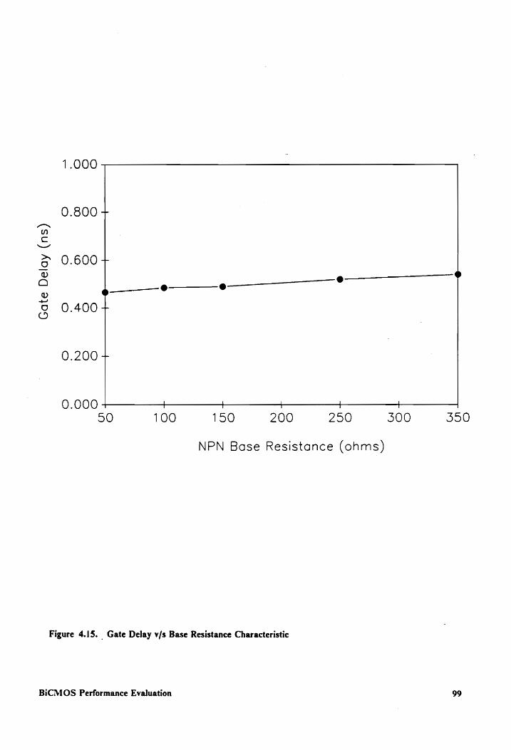
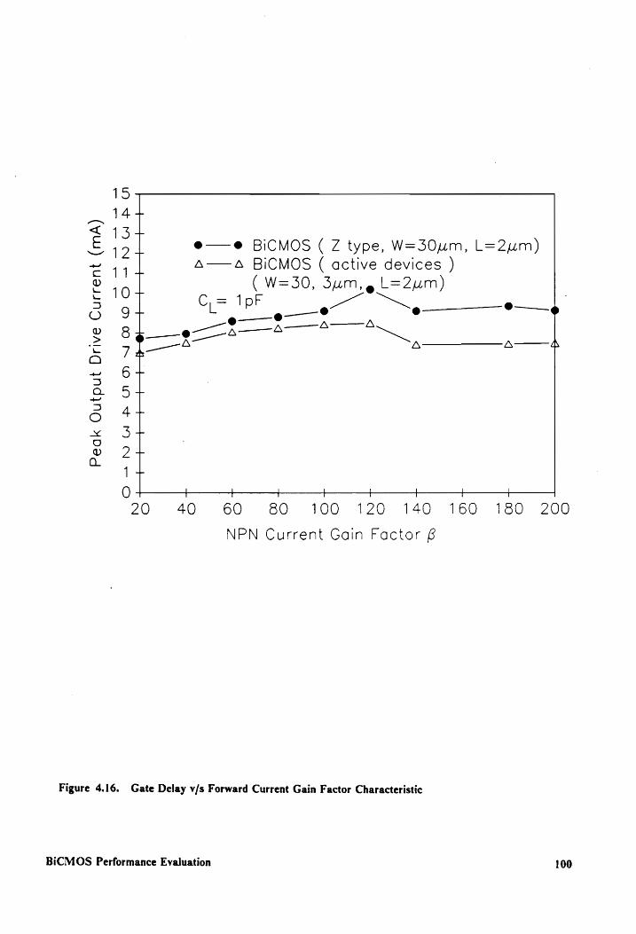
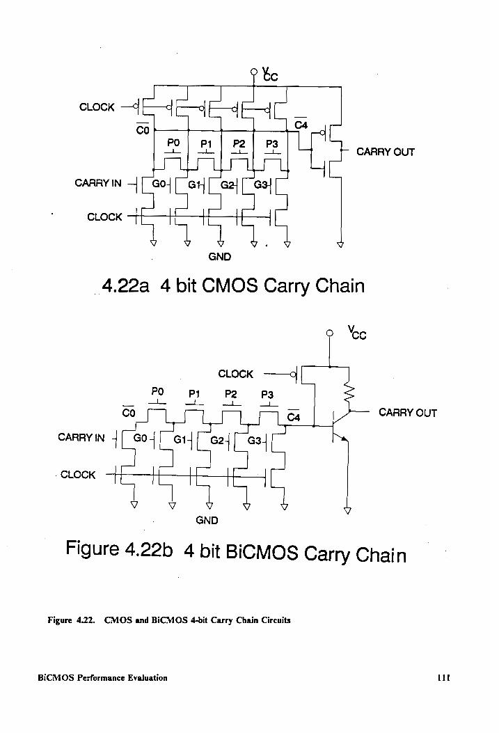
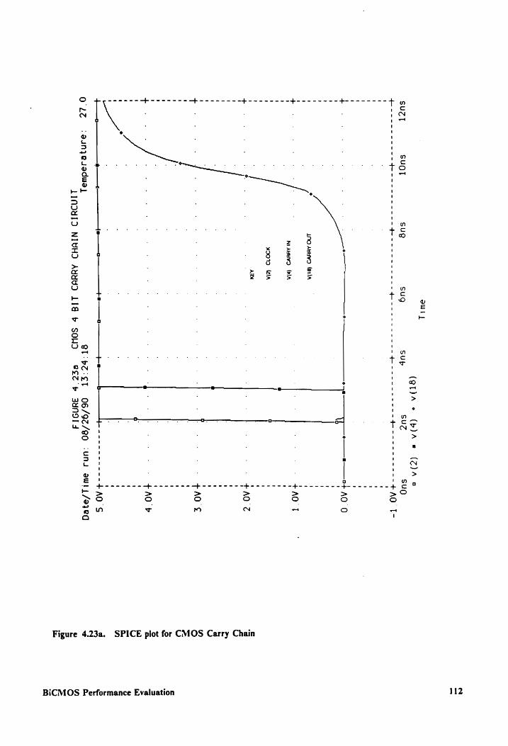
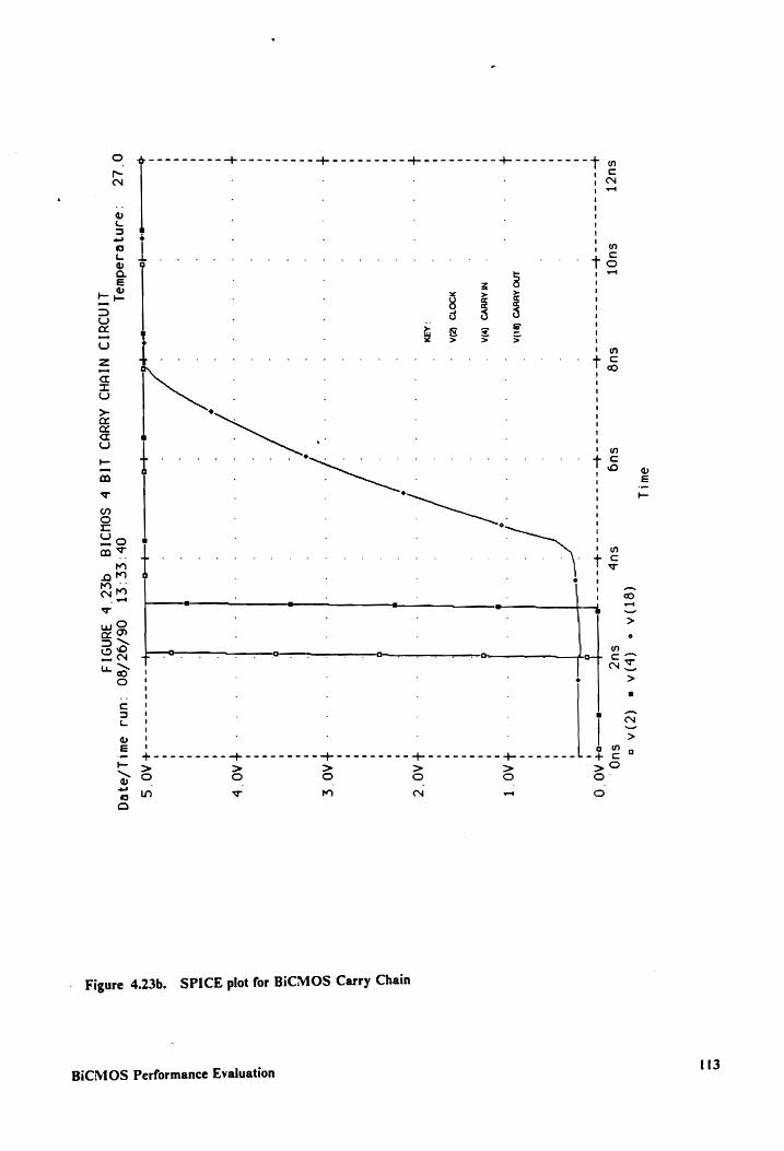
Page 1
ANALYTICAL MODELING AND SIMULATION OF BICMOS
FOR VLSI CIRCUITS
by
Prakash Narayanan
Thesis submitted to the Faculty of the
Virginia Polytechnic Institute and State University .
in partial fulfillment of the requirements for the degree of
Master of Science
in
Electrical Engineering
APPROVED:
Aicha bbshabini - Riad Dr. Aicha Elshabini-Riad, Chairperson
Qu L3Sspt <r LD Lo Dr. Joseph G. Tront Dr. Shinzo Onishi
September 6, 1990
Blacksburg, Virginia
Page 2
LS
Mus
\ah5
("40
N72
- DP
Page 3
ANALYTICAL MODELING AND SIMULATION OF BICMOS
FOR VLSI CIRCUITS
by
Prakash Narayanan
Dr. Aicha Elshabini-Riad, Chairperson
Electrical Engineering
(ABSTRACT)
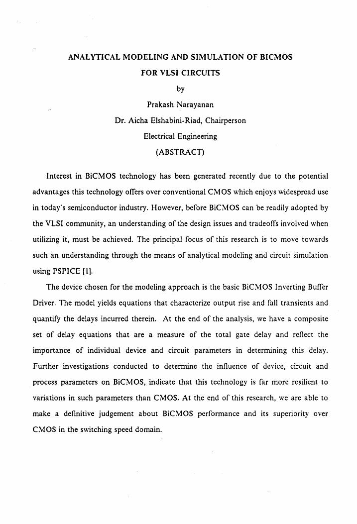
Interest in BiCMOS technology has been generated recently due to the potential
advantages this technology offers over conventional CMOS which enjoys widespread use
in today’s semiconductor industry. However, before BiCMOS can be readily adopted by
the VLSI community, an understanding of the design issues and tradeoffs involved when
utilizing it, must be achieved. The principal focus of this research is to move towards
such an understanding through the means of analytical modeling and circuit simulation
using PSPICE [1].
The device chosen for the modeling approach is the basic BiCMOS Inverting Buffer
Driver. The model yields equations that characterize output rise and fall transients and
quantify the delays incurred therein. At the end of the analysis, we have a composite
set of delay equations that are a measure of the total gate delay and reflect the
importance of individual device and circuit parameters in determining this delay.
Further investigations conducted to determine the influence of device, circuit and
process parameters on BiCMOS, indicate that this technology is far more resilient to
variations in such parameters than CMOS. At the end of this research, we are able to
make a definitive judgement about BiCMOS performance and its superiority over
CMOS in the switching speed domain.
Page 4
Acknowledgements
I] would like to thank all those who have contributed towards the completion of this
thesis. Special thanks are due to Dr. A. Elshabini-Riad, my principal advisor, for her
patience, guidance and invaluable suggestions. I would also like to thank the other
members of my committee, Dr. Joseph G. Tront, for his advice and instruction during
the VLSI design courses, and Dr. Shinzo Onishi for his assistance and comments.
I am also grateful for the support of my family and friends throughout this venture.
Acknowledgements iti
Page 5
Table of Contents
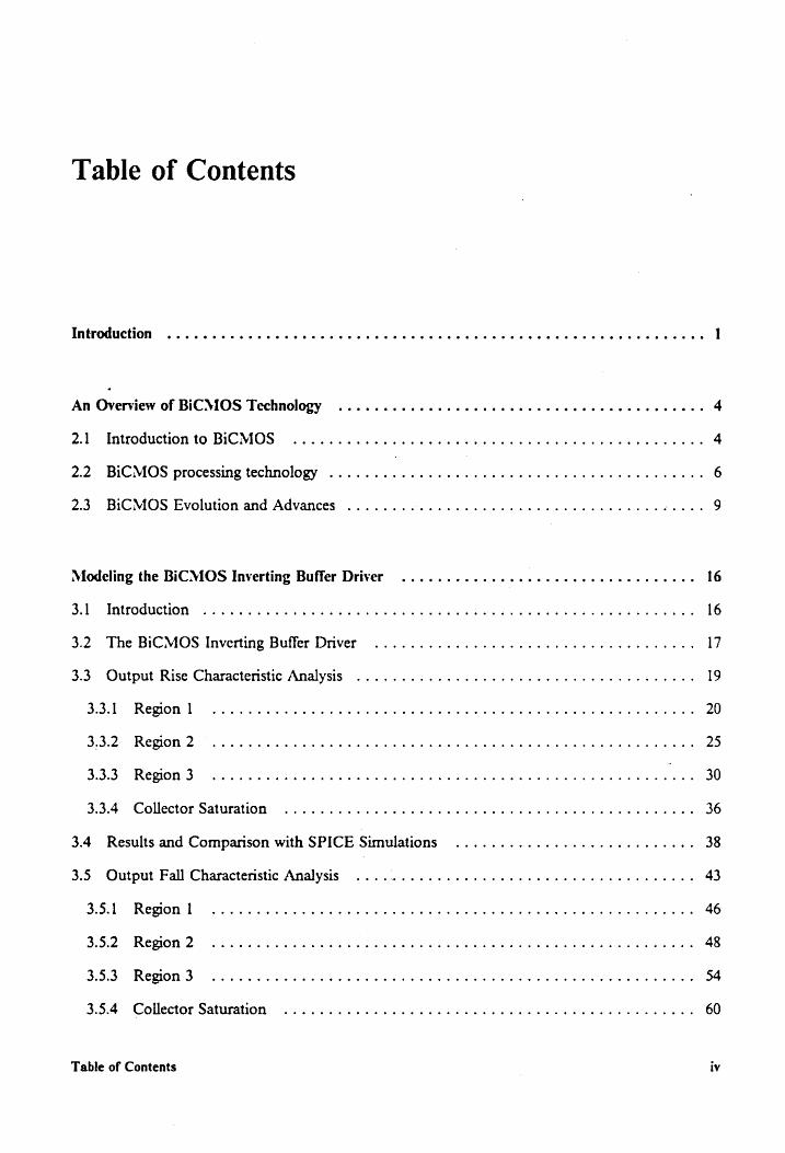
Introduction 0.0... ccc cece ccc cece eee ee eee eee eee eee eee eee eee scene 1
An Overview of BICMOS Technology .......... cece cc ec cece eee e eee weet a eeees 4
2.1 Introduction to BICMOS... 6... eee nee ee nnes 4
2.2 BiCMOS processing technology ....... Dene eee eee tee tent eee ees 6
2.3 BiCMOS Evolution and Advances .......... 0.0... eee ees -.... 9
Modeling the BICMOS Inverting Buffer Driver 2.0.0... 0. cc ccc eee ce eee rete eeee 16
3.1 Introduction 2.2... .. cee ee ene ee eee eee eee ees 16
3.2. The BiCMOS Inverting Buffer Driver ....... 20.0... cece eee ee ees 17
3.3 Output Rise Characteristic Analysis 2.0... 0.0.0. cece eee ee eee eens 19
3.3.1 Region 1] ...... eee ee ee ee ee ee eee eet eee eee 20
3.3.2 Region 2 ..... ccc ee ee ee eee ee eee ene nes 25
3.3.3 Region3 0.0... cece cece cece cece ese eeeeveeeeeeeeeeeennnnes 2. 30
3.3.4 Collector Saturation 2.0... ee etn eee eee eee 36
3.4 Results and Comparison with SPICE Simulations .........0eecceceeuseeeees 38
3.5 Output Fall Charactenstic Analysis . Le ee eee eee ee ee eee eens 43
3.5.1 Region) ... cece ee eee ee ee eee ee eee teen en eens 46
3.5.2 Region 2 0... . ccc cc ce ee ee eee eee ee eee eee ee eens 48
3.5.3 Region 3 ... cece ee ee ee ne eee eee tee teen ena 54
3.5.4 Collector Saturation 2.2... 2.0... ec ee ene eee neces 60
Table of Contents iv
Page 6
3.7 Summary 2... ee ee eee eee eee eee ene e ee eens 66
BiCMOS Performance Evaluation ....... 0... cece cee cece eee erect ee eee eee eees 69
4.1 Introduction 2.0... ccc ee eee eee nett ee een eee eee eee 69
4.2 Some Definitions ........... ee eee eee teen eee eee e nee 72
4.3. Effect of External Circuit Parameters and Operating Conditions .................. 75
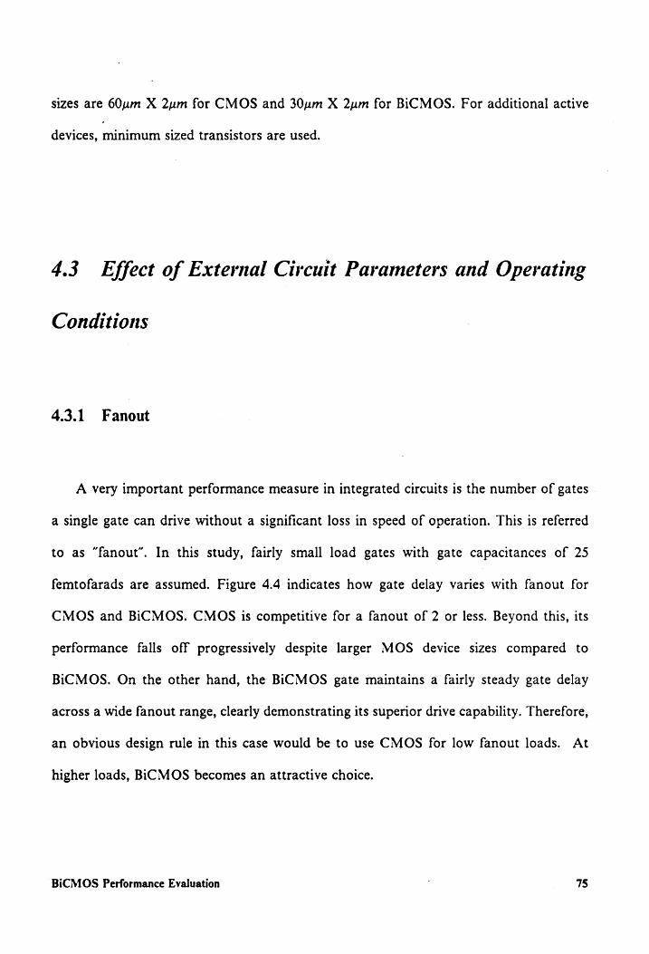
4.3.1 Famout 2.0... . ce ce ec ee en ee eee eee eee eee eee 75
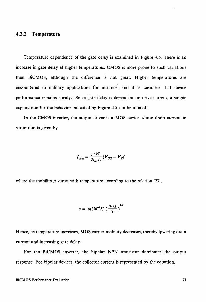
4.3.2 Temperature 2... .. 0. . cece ee eee eee ee eee eee eens 77
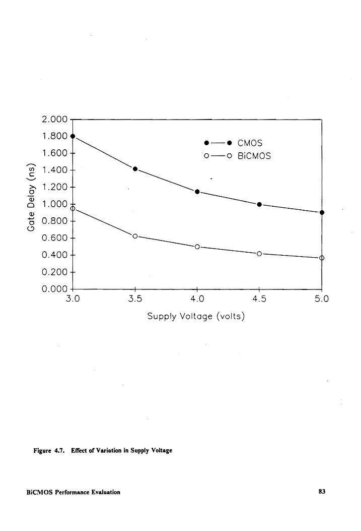
4.3.3 Supply Voltage Scaling ...... 0... cee ee ee tee eee ees 81
4.4 Influence of MOS Device Parameters ....... 0... cee cece eee teens 82
4.4.1 Oxide Thickness 0... 0.0... ccc cee e nee ene 82
4.4.2 Mobility 2.2... ee ee ne ee tee ete eee ene 84
4.4.3 MOS Device Scaling ........ 0... cece ee eee eee eee eee 88
4.4.4 Threshold Voltage 2.0.0.2... 0... ccc cc cee ee eee een ene eas 88
4.5 Influence of NPN Device Parameters ........ 2.0... eee eee eee eee eee 92
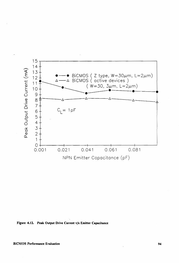
4.5.1 Emitter Design... 0... ccc ee eee nee e eee eee nenes 92
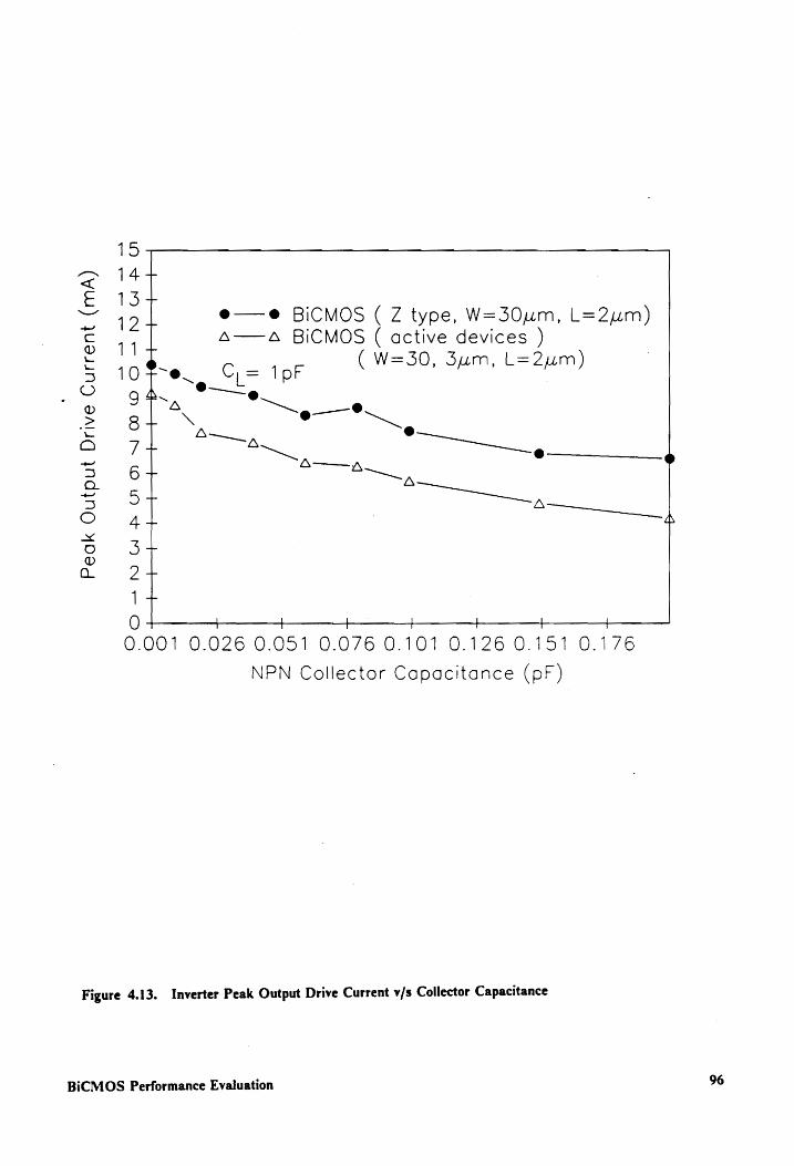
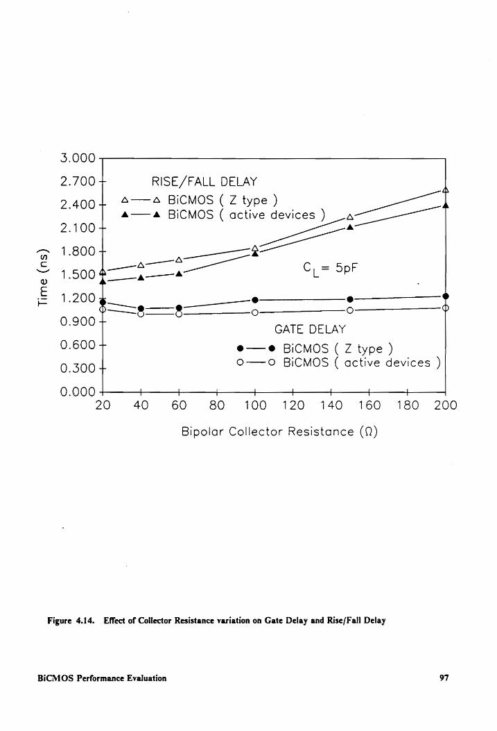
4.5.2 Collector Design 2.0... . ene en een eee ee eee e nee 93
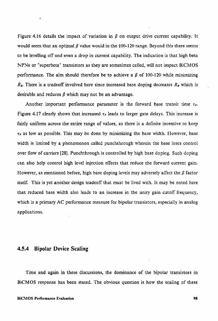
4.5.3 Base Design ......... ce cc ee eee ete ene eee ees 95
4.5.4 Bipolar Device Scaling ..... 0... 0... ccc eee een e nea 98
4.6 Inverter Types and Multi Input Gates ....... 2.0... 0. ee eee eee eee 103
4.7 BiCMOS Applications ....... 0... cece eee eee te een eee e nee eens 109
4.7.1 Digital BiCMOS ..... 0... cc ee eet ee ete een nees 109
4.7.2 Analog BICMOS ....... 0. ccc cc cece cece eee e eee eee eens 114
48 Summary 2... . ee ee ee ee ee eee eee eee eee eee 119
Conclusions 2.1... cc ccc ccc eet teeter tee eee eee tee etter teen eens 121
Table of Contents v
Page 7
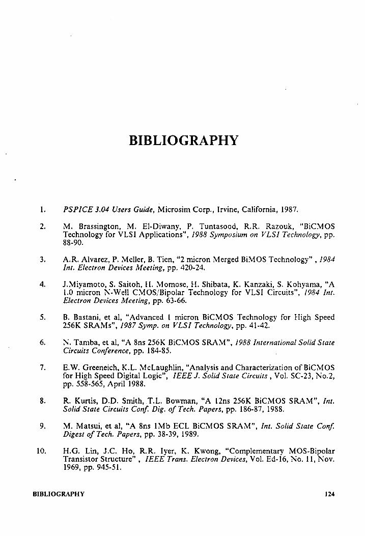
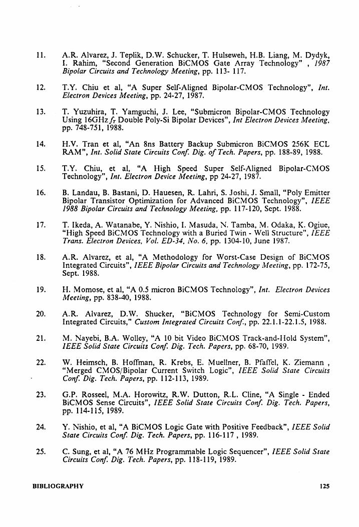
BIBLIOGRAPHY 2... ccc cc cece ee et eee eee eee eter eee eee ee eteee 124
Modeling Analysis Clarifications ........ cece ere cere sere rere ess eesteeee 127
A.1 s-domain derivation 2... 0... 0. ccc cece ee eee eee eee eee e eee enene 127
A.2. Taylor’s series simplification 2.0... 0... ccc ccc ee eee ete eee eens 129
A.3 Effect of incorporating simulation results into analytical equations .............. 130
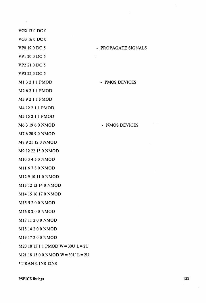
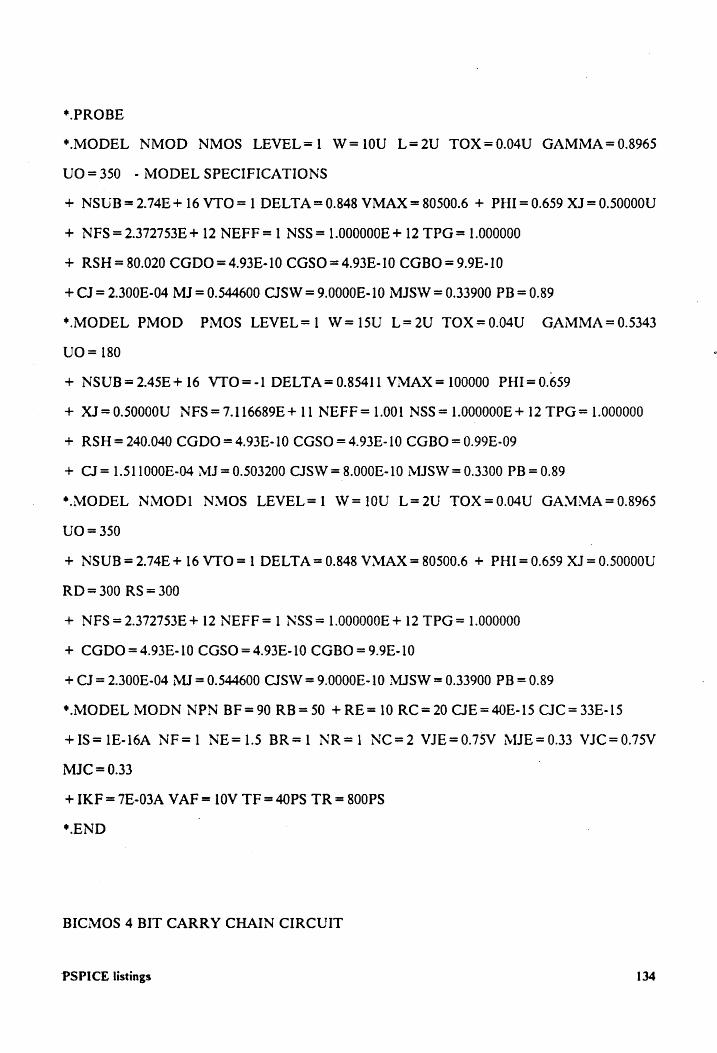
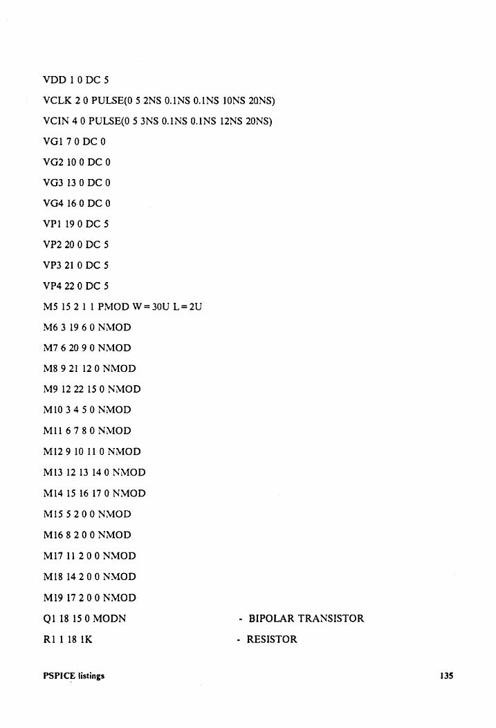
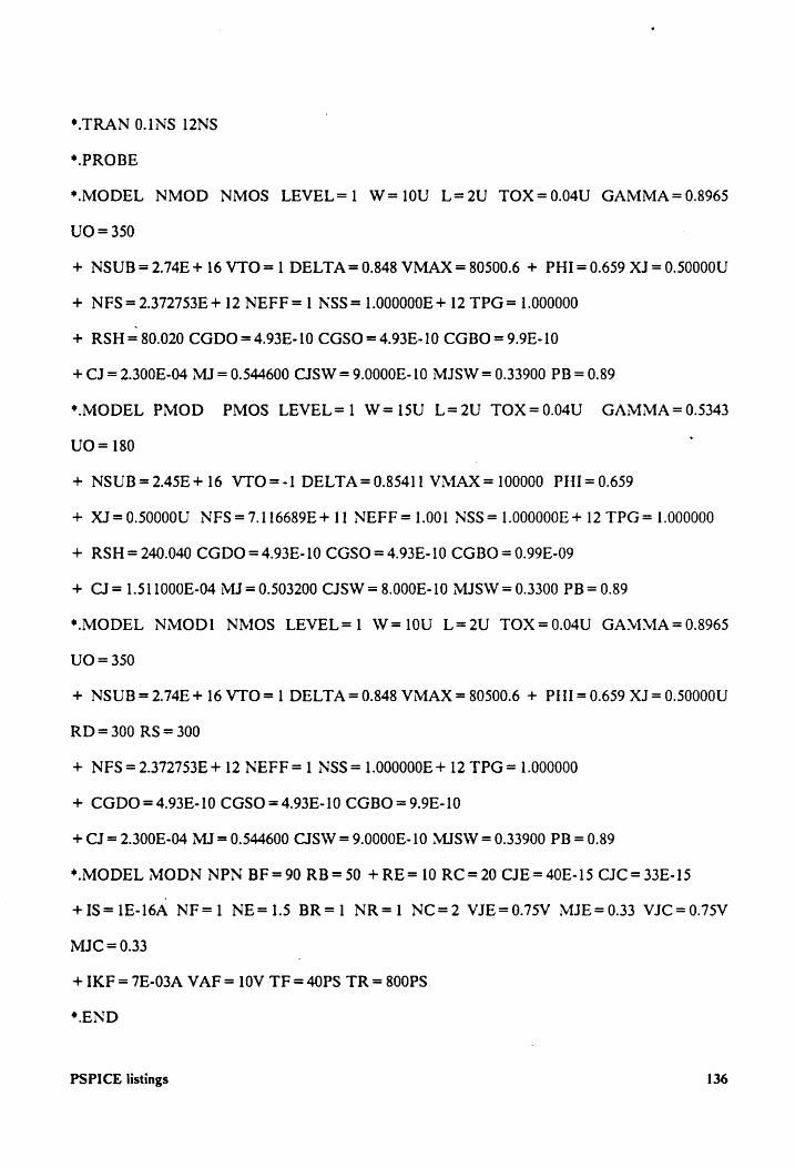
PSPICE listings ........ ccc cc ccc cee eee eee eee eee eee ee eee eee serene 132
0) ©: 139
Table of Contents vi
Page 8
List of Illustrations
Figure 2.1. CMOS and BiCMOS Device Structures .......... 0... cee eee eee 8
Figure 3.1. The BiCMOS Inverting Buffer Driver ............... tenes 18
Figure 3.2, Output Charging Circuit 2... 0... cc ee eee eee eee ee eens 21
Figure 3.3. Inverter Regions of Operation for Rising Output .............505 22
Figure 3.4. Region | circuit model and s-domain representation ...........4.. 23
Figure 3.5. Region 2 circuit model ......... cece ce ee eet eee eee eee nes 26
Figure 3.6. Region 3 circuit model ......... ccc cece eee eee eee eee eeee 31
Figure 3.7. Comparison of Analytical and SPICE results for Rise Analysis ...... 42
Figure 3.8. Output Discharge Circuit 2... . 0... ee eee ee ee eens sees . 44
Figure 3.9. Inverter Regions of Operation for Falling Output ................ 45
Figure 3.10. Region 1 circuit model and s-domain representation ............. 47
Figure 3.11. Region 2 circuit model 1.0... .. cece eee ee eee tee eas 49
Figure 3.12. Region 3 circuit model .......... cece eee eee eee eee 55
Figure 3.13. Comparison of Analytical and SPICE results for Fall Analysis ..... 67
Figure 4.1. Z-type BICMOS Inverter 2... 0... cece ee ee ee te eee 70
Figure 4.2. BiCMOS Inverter with Active Devices 2.1... 0... eee eee eee 71
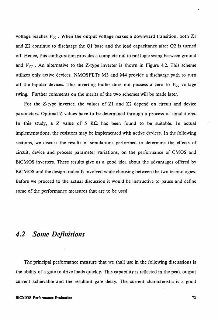
Figure 4.3. Definition of Gate Delay and Peak Output Drive Current .......... 74
Figure 4.4. Gate Delay v/s Fanout Characteristic ........... 0. ce eee eee eee 76
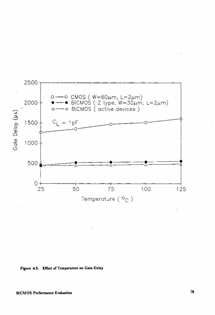
Figure 4.5. Effect of Temperature on Gate Delay ......... 0. cece seen eee 78
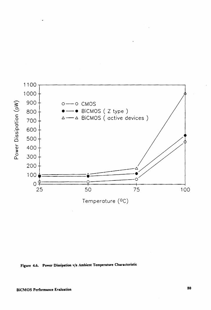
Figure 4.6. Power Dissipation v/s Ambient Temperature Characteristic ......... 80
Figure 4.7. Effect of Variation in Supply Voltage. Sete ee eet eee teense 83
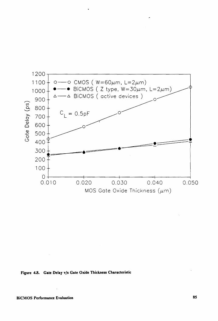
Figure 4.8. Gate Delay v/s Gate Oxide Thickness Characteristic .........+.... 85.
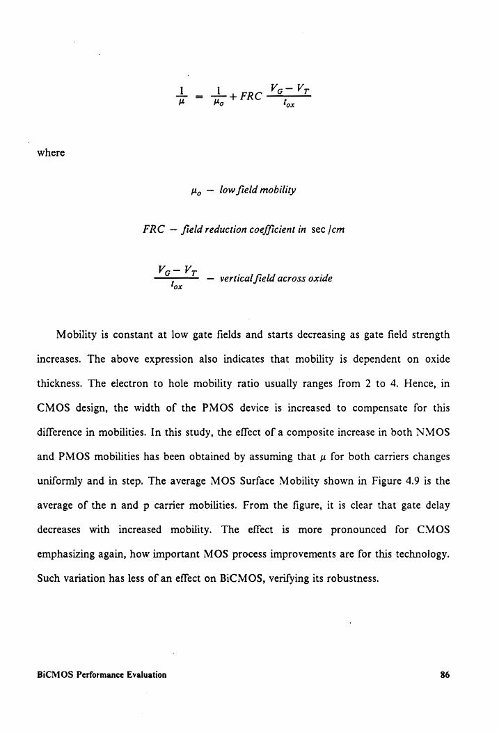
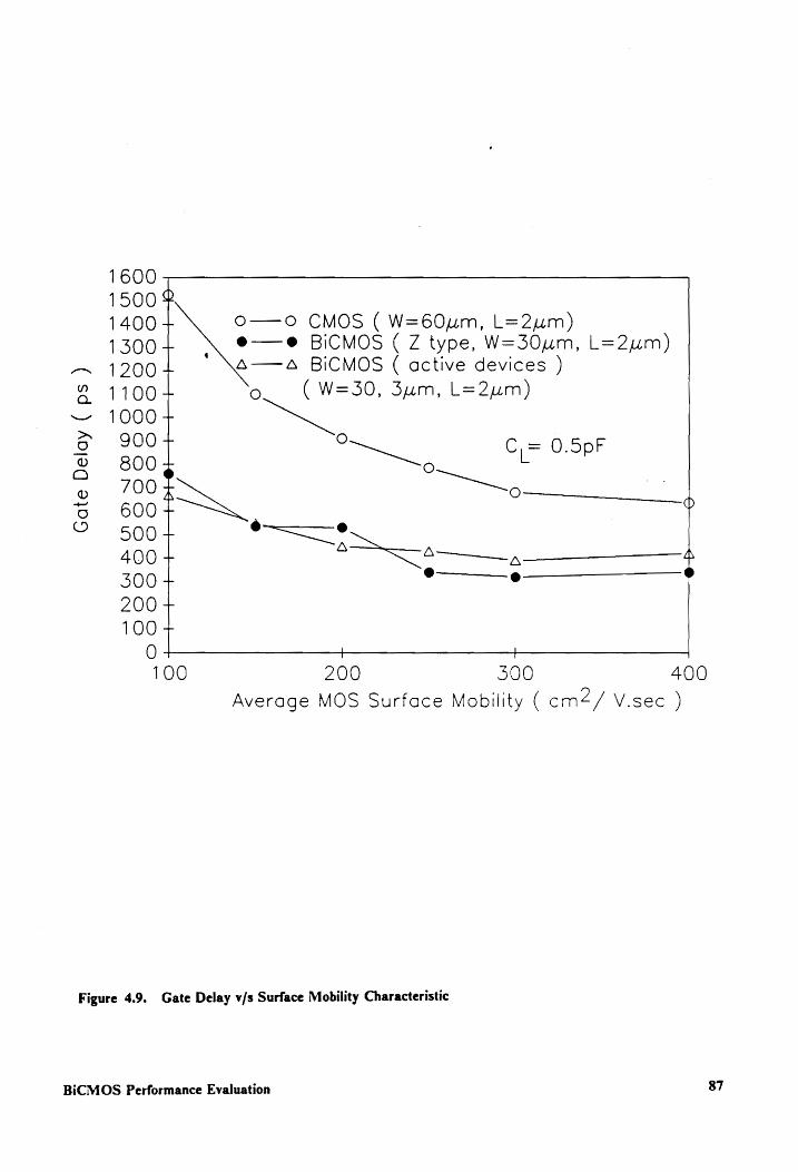
Figure 4.9. Gate Delay v/s Surface Mobility Characteristic ......... 00 eeees 87
List of Hiustrations . vii
Page 9
Figure 4.10,
Figure 4.11.
Figure 4.12.
Figure 4.13.
Figure 4.14.
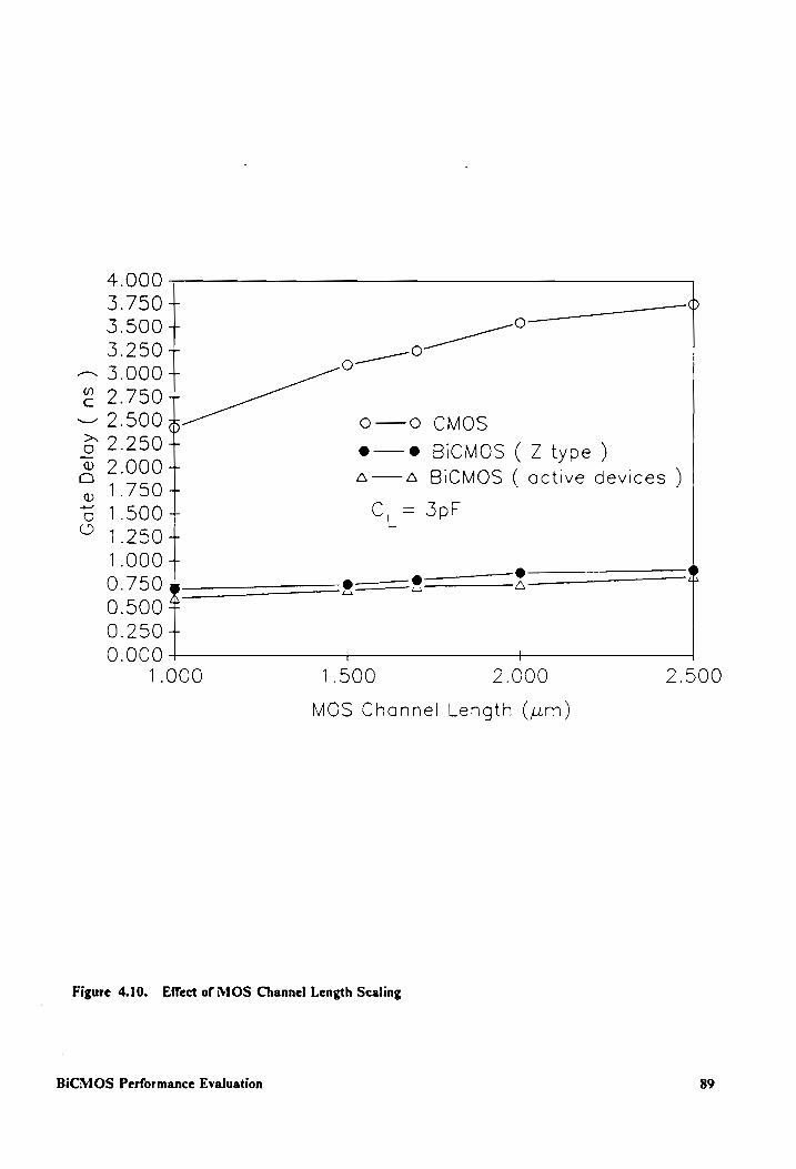
Effect of MOS Channel Length Scaling ....... 0... 0. cc cece eeeas 89
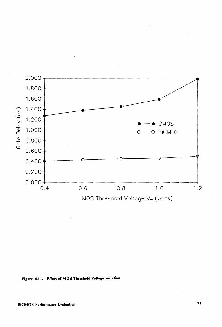
Effect of MOS Threshold Voltage variation .............0 ce eaee 91
Peak Output Drive Current v/s Emitter Capacitance ............. 94
Inverter Peak Output Drive Current v/s Collector Capacitance ..... 96
Effect of Collector Resistance variation on Gate Delay and Rise/ Fall Delay oo c ccc ccc cee eee ee eee eee tee eee ee ee eee ees 97
Figure 4.15. Gate Delay v/s Base Resistance Characteristic ........... 2000008 99
Figure 4.16. Gate Delay v/s Forward Current Gain Factor Characteristic ...... 100
Figure 4.17. Gate Delay v/s Forward Base Transit Time Characteristic ........ 101
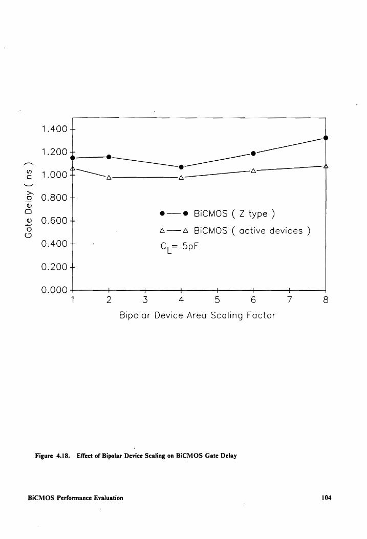
Figure 4.18. Effect of Bipolar Device Scaling on BiCMOS Gate Delay ........ 104
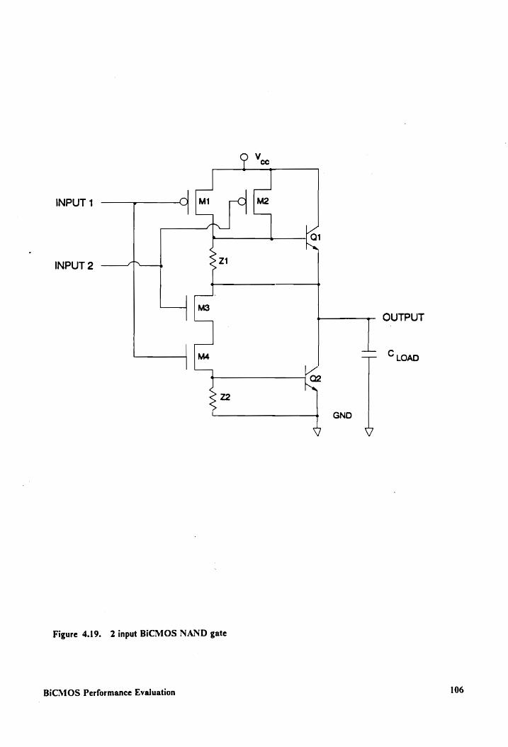
Figure 4.19. 2 input BICMOS NAND gate ........ 0. ccc eee eee eee eens 106
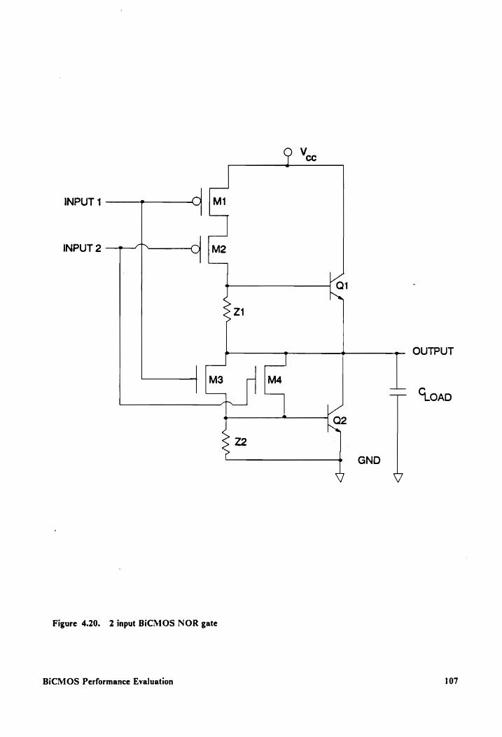
Figure 4.20. 2 input BiCMOS NOR BALE cece eee ete ee eee ees 107
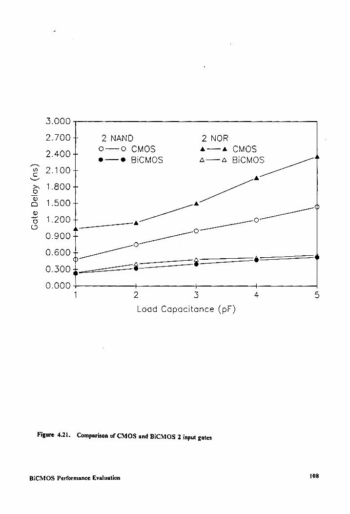
Figure 4.21. Comparison of CMOS and BiCMOS 2 input gates ............. 108
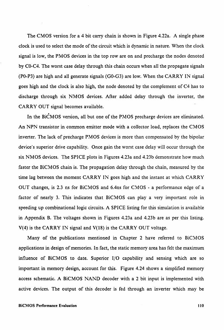
Figure 4.22. CMOS and BiCMOS 4-bit Carry Chain Circuits ...........000. 111
Figure 4.23a. SPICE plot for CMOS Carry Chain ....... 2. cee eee cee eee 112
Figure 4.23b. SPICE plot for BICMOS Carry Chain .......... 0.00000 e eae 113
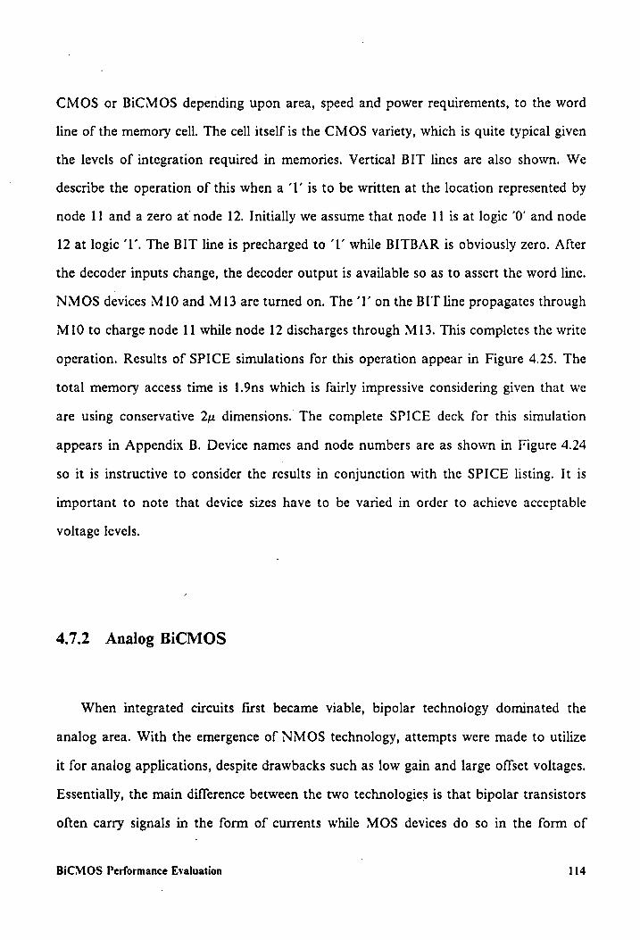
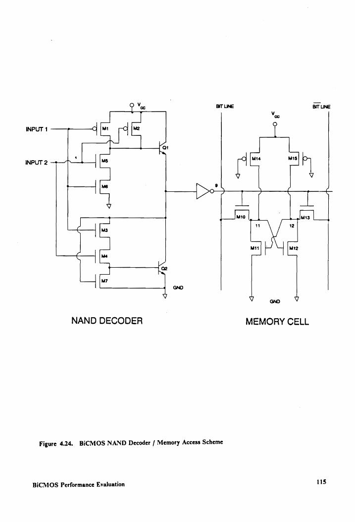
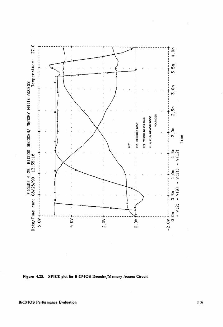
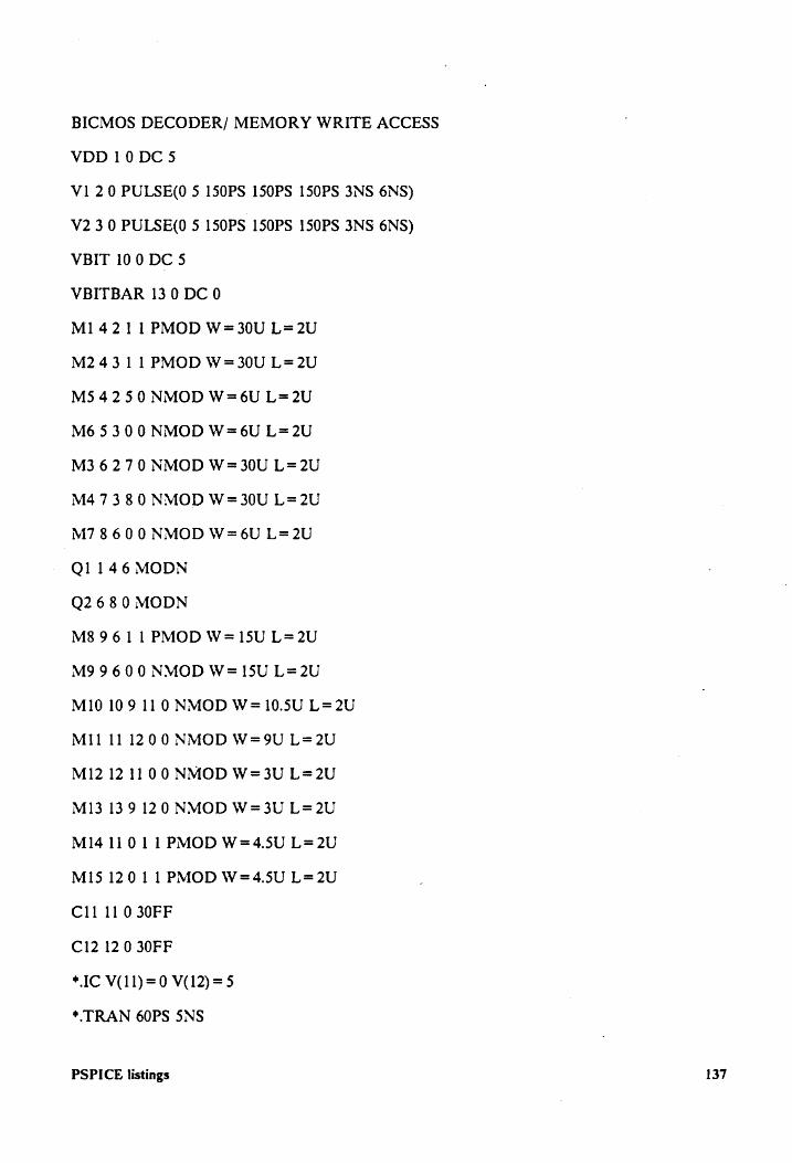
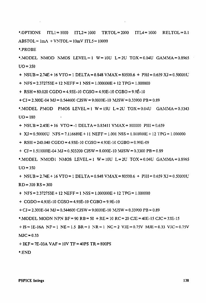
Figure 4.24. BICMOS NAND Decoder / Memory Access Scheme ............ 115
Figure 4.25. SPICE plot for BK\CMOS Decoder/Memory Access Circuit ....... 116
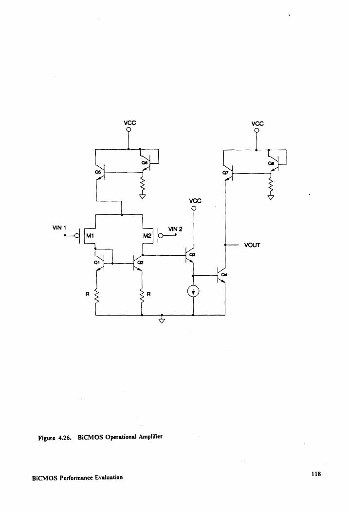
Figure 4.26. BiCMOS Operational Amplifier 2... 0.0... 0. cee eee eee ee eee 118
List of Illustrations viii
Page 10
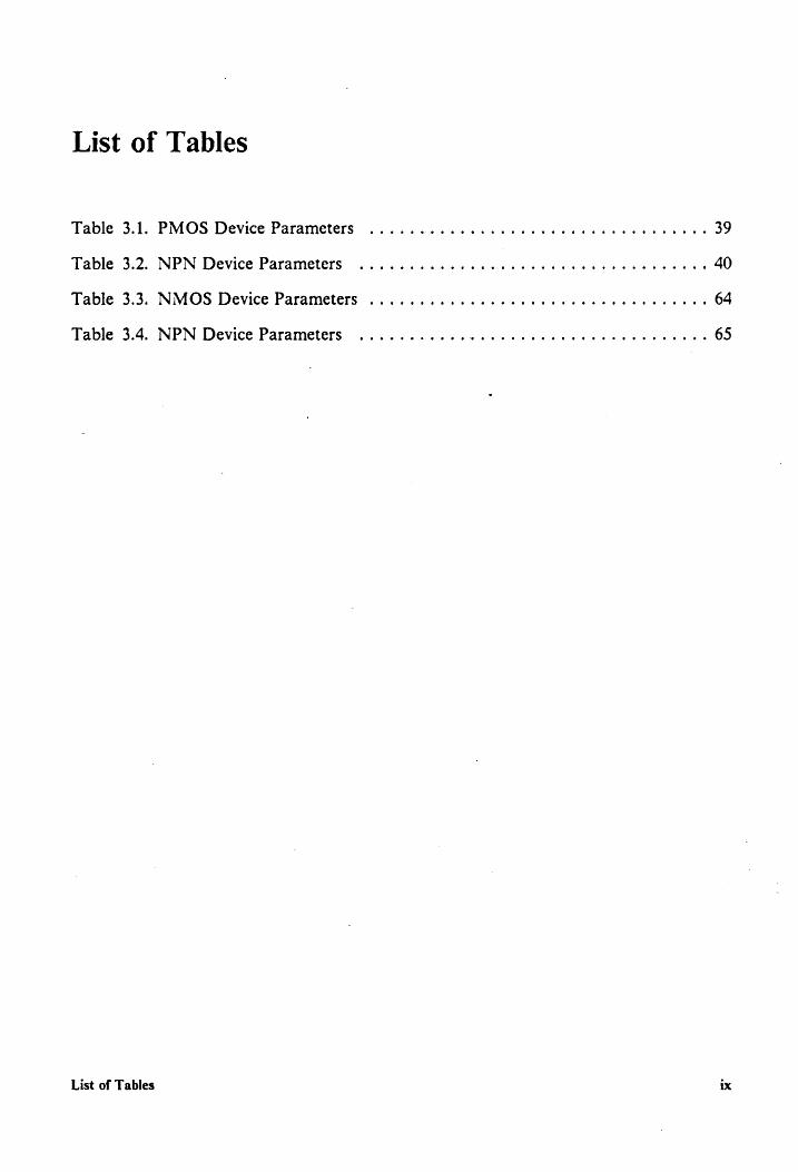
List of Tables
Table 3.1. PMOS Device Parameters .......... cece ee eee eee ee eee ee eee 39
Table 3.2. NPN Device Parameters ......... cece eee eee cee eee teen eens 40
Table 3.3. NMOS Device Parameters ..... 0... cc eee e ee eee eee eee eee eens 64
Table 3.4. NPN Device Parameters ....... 0. cece eee ee eee ete e erences 65
List of Tables ix
Page 11
Chapter 1
Introduction
BiCMOS is the newest technology to emerge on the VLSI horizon and promises to
deliver better performance than CMOS, which currently dominates the VLSI market.
Although the idea of integrating MOS and bipolar devices on a common wafer was
proposed two decades back, it is only recently that commercial offerings utilizing
BiCMOS have become available. However, before BICMOS can become a major player
in the VLSI market, a thorough understanding must be achieved regarding the design
and processing tradeoffs involved when MOS and bipolar technologies are integrated.
The principal aim of this research is to understand and evaluate BiCMOS technology
through the methods of analytical modeling and circuit simulation.
Chapter 2 of this thesis provides a broad overview of BiCMOS and the potential
benefits of utilizing it. The issues entailed by a shift to this technology and the historic
precedent of the move to CMOS from NMOS are mentioned. The importance of
processing technology in making BiCMOS a viable proposition is discussed and a brief
description of fabrication techniques is provided. A review of the evolution of this
Introduction 1
Page 12
technology and recent developments in its implementation are also a subject of
discussion.
Chapters 3 and 4 document the research that has been performed to model and
simulate BiCMOS in order to determine the process, device and circuit parameters that
influence its performance. In Chapter 3, the basic BiCMOS inverting buffer driver circuit
is modeled analytically [7]. Both rising and falling output waveforms are considered. The
step-by-step derivation explains the different regions of operation of the MOS and
bipolar devices forming this circuit. The analysis itself is divided into different regions in
time and models for each of these regions are described. The final products of the
modeling process are sets of equations representing the change in the output voltage and
the propagation delay through the gate, both in terms of circuit and device parameters.
PSPICE simulations are then used to validate these theoretical results. Deviations, if
any, are accounted for and justified. The modeling process provides us with insights
about operation of the inverting buffer at the transistor level. It also helps us obtain a
set of delay equations that allow a first approximation of gate delay to be made.
Information regarding important parameters that affect this delay is also available.
The principal aim of Chapter 4 is to evaluate BiCMOS technology in relation to
CMOS which is currently the most popular VLSI technology. The PSPICE circuit
simulator is used as a tool for this evaluation [1]. Circuit simulators enable us to make
accurate predictions about circuit performance without having to actually fabricate and
test them - an expensive process given the type of technology we are dealing with.
Derivatives of the SPICE circuit simulator are used almost universally for this purpose.
PSPICE is one such popular version. The effects of variation in circuit, device and
process parameters on BiCMOS performance are sought to be determined. Both MOS
and BJT parameters are considered and results are viewed in the light of established
analytical equations. Design issues, and tradeoffs necessitated by these results are also
Introduction 2
Page 13
discussed. Further studies are conducted regarding the switching characteristics of multi
input BiCMOS gates and practical VLSI implementations of this technology. A
definitive judgement about BiCMOS performance and its superiority over CMOS is then
‘made.
Chapter 5 documents the conclusions that can be drawn from the analytical
modeling and performance evaluation processes. A summary of the research performed
and inferences drawn regarding BiCMOS is presented.
Introduction 3
Page 14
Chapter 2
An Overview of BiCMOS Technology
2.1 Introduction to BiCMOS
VLSI technology is constantly pushing towards new frontiers and the two main
performance measures that characterize this advance are switching speed and power
dissipation of devices. Traditionally, bipolar technology has demonstrated superior speed
while MOS devices have always dissipated less power. These two technologies have
evolved independently and carved specific applications for themselves. Bipolar chips
have dominated markets such as fast memories, video signal processing and sensing
while MOS chips are popular for slower but denser memories, gate arrays and
microprocessors among others.
More specifically bipolar devices have an advantage in switching speed, analog
capability and I/O (input-output) speed. MOS technology, now dominated by CMOS,
scores in areas such as low power dissipation, noise margins and packaging density.
An Overview of BiCMOS Technology 4
Page 15
Additionally, the ability to integrate large, complex functions with high yields has
resulted in CMOS far exceeding bipolar products with regard to volume of chips in
today’s market. CMOS technology has consistently been improved and scaled down in
dimensions to yield high performance VLSI. Now, there is a feeling that CMOS
fabrication technology may be pushing the limits of the laws of device physics and that
new Strategies must be devised. This forms the basis for a move towards BiCMOS.
The success of BiCMOS hinges on the ability to combine bipolar and CMOS
technologies on the same wafer and obtain superior performance that would otherwise
require super high density and expensive CMOS techniques. Bipolar processing
techniques have always been more complex than CMOS processing methods. The
principal tradeoff in BiCMOS is between additional process complexity and enhanced
performance. In many ways, the argument to move towards BiCMOS is very simular to
that which prompted the shift towards CMOS from NMOS in the early eighties. NMOS
was the original VLSI MOS technology and remained dominant until density and power
restraints suggested a move to CMOS with its ratioless logic style and near zero static
power dissipation. NMOS proponents argued that process complexity and associated
costs ruled out any serious challenges from CMOS. But, with advances in processing
methods, CMOS soon caught up and then surpassed NMOS to become the dominant
VLSI technology. BiCMOS poses the same kind of challenge to CMOS. Once again, as
CMOS requires increased process complexity to deliver improved performance, its
principal cost edge over BiCMOS will erode. In fact, the superior performance of
BiCMOS can delay the move towards smaller dimensions and thereby extend the life of
existing fabrication lines. There are also other advantages such as use of the bipolar
epitaxial layer to suppress latchup which has been the single biggest negative factor for
CMOS.
An Overview of BiCMOS Technology 5
Page 16
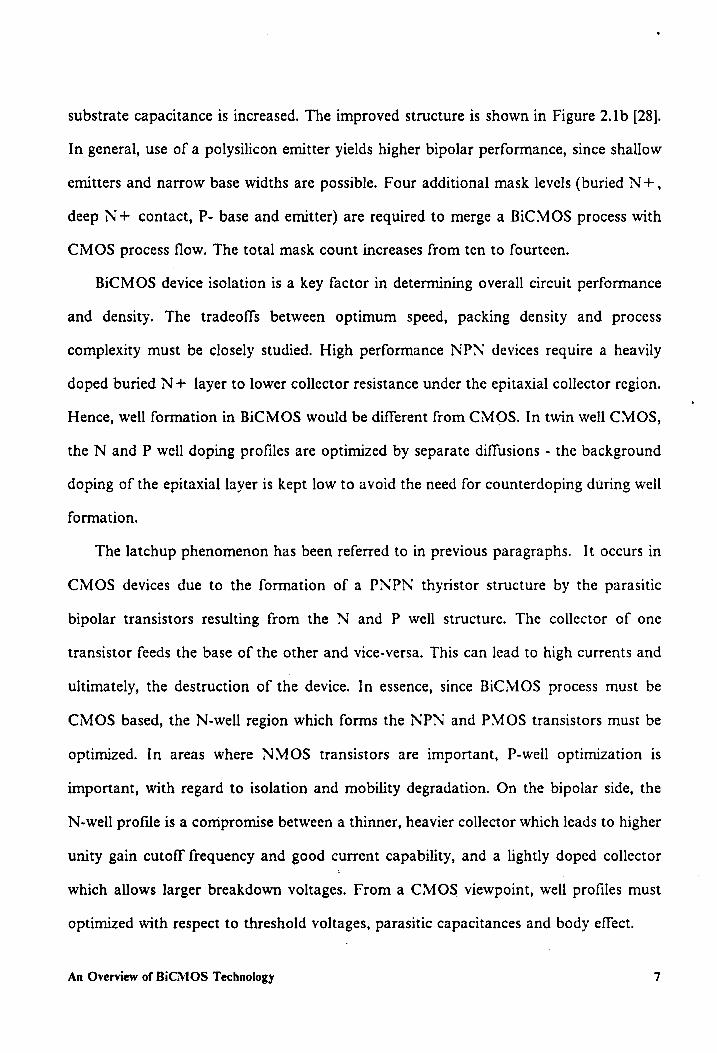
2.2 BiCMOS processing technology
Processing methods are the key to the success of BiCMOS since they will determine
the viability of combining the two technologies on the same wafer. Therefore, it would
be instructive to take a look at some of the strategies that may be employed for the
purpose. In general, the approach while designing with BiCMOS would be to use bipolar
devices in areas where speed is critical and MOS devices elsewhere. Hence, BiCMOS
processes would utilize a base CMOS process with additional steps to realize bipolar
devices.
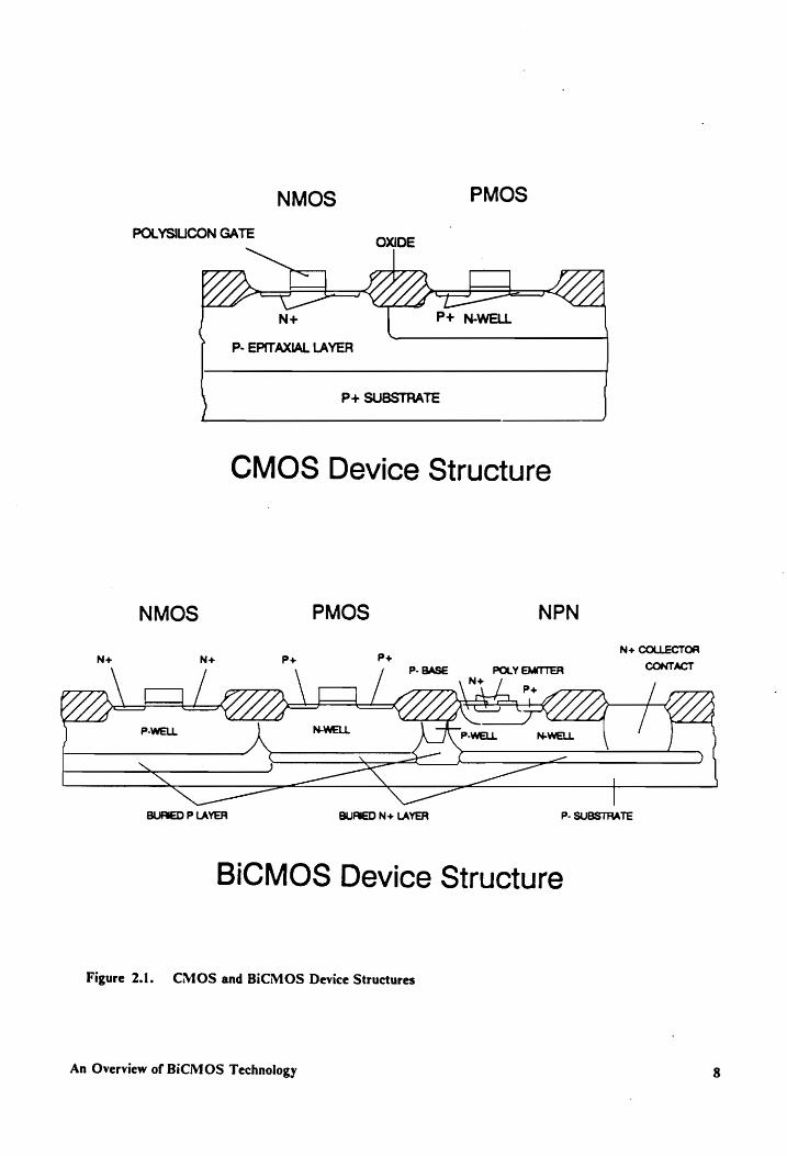
A typical N-well CMOS process that may be modified for BiCMOS is shown in
Figure 2.la [28]. The n channel device is built on a P- epitaxial layer which lies on a P+
substrate. The p channel device is built in an implanted N-well. The P+ substrate helps
reduce latchup by by providing a low impedance path through the vertical parasitic PNP
transistor that causes it. The bipolar device may be added to this structure by using the
PMOS N-well as the collector of the bipolar device and introducing an additional mask
level for the P- base region. However, the N-well collector in this case would be lightly
doped leading to high collector resistance which is undesirable. This may be overcome
by introducing a buried N+ layer under the N-well. This layer also helps control latchup
which means that the P- epitaxial layer on the heavily doped P+ substrate can be
replaced by a P- substrate. A drawback of this approach is that P- substrate doping
levels limit packing density. Increase in these levels leads to higher collector-to-substrate
capacitance. Also, the N type epitaxial layer has to be counterdoped to isolate the
N-well regions (P-wells for NMOS devices).
A solution to the above problems would be to self-align buried P layers to buried
N+ regions. Bipolar packing density is improved by this step. However, collector to
An Overview of BiCMOS Technology 6
Page 17
substrate capacitance is increased. The improved structure is shown in Figure 2.1b [28].
In general, use of a polysilicon emitter yields higher bipolar performance, since shallow
emitters and narrow base widths are possible. Four additional mask levels (buried N+,
deep N+ contact, P- base and emitter) are required to merge a BiCMOS process with
CMOS process flow. The total mask count increases from ten to fourteen.
BiCMOS device isolation is a key factor in determining overall circuit performance
and density. The tradeoffs between optimum speed, packing density and process
complexity must be closely studied. High performance NPN devices require a heavily
doped buried N+ layer to lower collector resistance under the epitaxial collector region.
Hence, well formation in BiCMOS would be different from CMOS. In twin well CMOS,
the N and P well doping profiles are optimized by separate diffusions - the background
doping of the epitaxial layer is kept low to avoid the need for counterdoping during well
formation.
The latchup phenomenon has been referred to in previous paragraphs. It occurs in
CMOS devices due to the formation of a PNPN thyristor structure by the parasitic
bipolar transistors resulting from the N and P well structure. The collector of one
transistor feeds the base of the other and vice-versa. This can lead to high currents and
ultimately, the destruction of the device. In essence, since BiCMOS process must be
CMOS based, the N-well region which forms the NPN and PMOS transistors must be
optimized. In areas where NMOS transistors are important, P-well optimization is
important, with regard to isolation and mobility degradation. On the bipolar side, the
N-well profile is a comipromise between a thinner, heavier collector which leads to higher
unity gain cutoff frequency and good current capability, and a lightly doped collector
which allows larger breakdown voltages. From a CMOS viewpoint, well profiles must
optimized with respect to threshold voltages, parasitic capacitances and body effect.
An Overview of BiCMOS Technology 7
Page 18
NMOS PMOS
POLYSILICON GATE
™
LPS | N+ P+ N-WELL
OXIDE
P- EPITAXIAL LAYER
P+ SUBSTRATE
CMOS Device Structure
BURIED P LAYER BURIED N+ LAYER P- SUBSTRATE
BiCMOS Device Structure
Figure 2.1. CMOS and BiCMOS Device Structures
An Overview of BiCMOS Technology 8
Page 19
2.3 BiCMOS Evolution and Advances
The potential advantages of combining bipolar and MOS devices on the same chip
were realized in 1969 [10]. The aim was to utilize the desirable features of both
technologies. Common collector NPN devices were fabricated using a diffused N+
source-drain region as emitter, a diffused P- isolation region as base and a N- substrate
as collector. Fabrication of a lateral NPN transistor is also described. The first industrial
BiCMOS offerings were operational amplifiers in the mid-1970s, by RCA [28]. Stanford
University and Texas Instruments developed the BIDFET technology that was used in
analog and power applications such as display drivers and voltage regulators. The thrust
towards digital BiCMOS began only in the mid-80s with Hitachi, Toshiba and Motorola
being the major players. For the remaining part of this section, we shall review
developments in BiCMOS with specific references to processing techniques, memory
design and other VLSI applications.
The static RAM area has probably felt the impact of BiCMOS more than any other
category of VLSI chips. The most common approach to date has been to use BICMOS
in the critical delay paths and I/O while designing the memory cell in pure CMOS. A
number of innovative designs with excellent performance have been reported. The
discussion in [5] indicates that MOS technology provides the most straightforward and
highest density memory array for static RAM (SRAM) design. The high performance
area is dominated by emitter coupled logic (ECL). An advanced lum BiCMOS
technology for a 256K SRAM is described. The process is an optimized 16 mask, double
poly Si, double metal sequence. Effective channel length is 0.64. for NMOS and 0.7um
for PMOS devices. The effect of both phosphorus and arsenic dopants to form
polysilicon emitters, is described.
An Overview of BiCMOS Technology 9
Page 20
Another 256K SRAM with lum technology is discussed in [6]. The use of a poly
emitter helps achieve a cutoff frequency of 9GHz. Effective channel lengths are 0.9um
for NMOS and l.lum for PMOS. A detailed schematic of the memory cell and I/O
buffering is provided. Active power levels of 400mW and standby power of 150mW are
reported. More 256K SRAM developments using BiCMOS technology, resulting in a
die size of 213 mils X 356 mils have taken place [8]. The basic memory cell size is 6.7
um X 14.4um. A different approach has led to the development of a 512K RAM with
both BiCMOS and ECL logic used [33]. A Sns address time and 2ns write time have been
achieved. The logic gate has a 150ps propagation delay and amW power dissipation. A
combined memory-logic array configuration is adopted to reduce interconnection delays.
0.8um BiCMOS with triple level polysilicon and aluminum is used. Bipolar base
resistance and parasitic capacitances are reduced by an emutter-base self aligned
structure and scaled down design rules. A 300 ohm base resistance and 11GHz cutoff
frequency are achieved. Gate thickness for MOS devices is 20 nm.
Use of ECL need not be restricted to the peripheral circuits [34]. This design of a
3.5ns, 500mW 16K RAM uses wired OR logic and cascode differential amplifiers to
achieve high speed. 0.54 BiCMOS technology is used with a self aligned structure
between the emitter and base electrode. A 8ns 1 megabit ECL BiCMOS RAM has also
been developed [36]. The process is 0.8um BiCMOS. This memory utilizes a 76 pm? full
CMOS six transistor memory cell, a dual MOS current source BiCMOS sensing scheme,
a BiCMOS current voltage reference network and a low capacitance decoding scheme
to achieve a 8ns delay. The configurable memory architecture allows expandibility up to
1Mb in units of 64Kb.
It has been mentioned that the ultimate factor deciding the success of BiCMOS
would be processing technology. It is no surprise therefore that a number of innovative
techniques have emerged here. A process utilizing high performance NPN devices has
An Overview of BICMOS Technology 10
Page 21
been described [2]. Effective channel lengths for MOS devices are 0.5um. The structure
enables high integration and low power to be achieved making it an ideal candidate for
high speed logic circuits. It features single level polysilicon with double metal and
vertical NPN transistors with walled, self aligned poly emitters. Optimal buried contacts
are used between the polysilicon and all junctions on the silicon substrate. An early
BiCMOS offering involved a 2um process with 2 mask steps added to a two layer metal
N well silicide CMOS process in order to fabricate poly emitter transistors [3]. Latchup
is minimized by adding a lum epitaxial layer and adopting a retrograde P-well. The
overall process flow attempts to achieve MOS and bipolar device compatibility. The
performance of MOS devices at subthreshold voltages has been detailed.
A 0.8m process used to fabricate a 117m? memory cell has been described in [14].
The cell employs a TiN interconnect to achieve a 5.6um X 20.9um size. Bipolar devices
are used mainly in the decoder and buffer circuits. A buried N+ layer and twin well
structure is formed by implantation into a thin, intrinsically doped epitaxial layer. The
process is single metal and double poly. A new non-overlapping super self-aligned
structure (NOVA) has been proposed in [15]. The PMOS and NPN devices are built in
the N-well with a buried layer. The low resistance N-wells suppress latchup and reduce
collector resistance. An arsenic doped polysilicon gate is used. Effective channel lengths
of 0.85 are achieved for the MOS devices. Bipolar current gain of 100 and gate delay
of 122ps are reported. A 0.84 BiCMOS process with high unity gain cutoff frequency
fr has been developed [13]. An ion implanted emitter helps reduce costs. Arsenic is
directly implanted to the substrate while an aluminum electrode is directly contacted to
the emitter N+. Twin well CMOS with channel lengths of 0.84m and lum and
threshold voltages of +0.8V and -0.8V are achieved for NMOS and PMOS devices
respectively. f; of 7.5 GHz is reported. The paper suggests that in general, for a high
speed sub micron BiCMOS gate, an ion implanted emitter with a buried N+ layer and
An Overview of BICMOS Technology 11
Page 22
deep N+ collector is suitable. An interesting evaluation of phosphorus and arsenic
doped emitters for a lum BiCMOS process appears in [17]. The process utilizes 16 mask
levels, double level polysilicon and 2 levels of metallization. A 1.5um epitaxial layer is
combined with a N+ buried layer to provide an effective low resistance collector. The
base implant is decided by the type of poly emitter. The phosphorus doped emitter can
result in high emitter sheet resistance but lowers base resistance and is easier to
manufacture. Use of phosphorus also allows better forward current gain and base transit
time performance. Arsenic on the other hand, enables af; of 11.2GHz to be obtained,
whereas this figure for phosphorus is only 3.2GHz.
In addition to memory design and processing publications related to BiCMOS
applications in other fields are also available. A general procedure for worst case
BiCMOS design is suggested in [18]. The methodology takes into account physical
correlation between NPN and CMOS model parameters and results in a self consistent
set of parameters for circuit simulations. Tradeoffs between FET and BJT design are
discussed. The ‘corners’ approach which entails perturbation of a mintmum number of
parameters in a device model to simulate worst case conditions, is adopted. A general
discussion on requirements for semi-custom BiCMOS is presented in [20]. It is proposed
that three basic BiCMOS technologies will evolve - high performance, low cost and
analog compatible. A suggestion that a 20-25% increase in die cost will result which can
be justified only by performance improvements of 50% or more, is made. Judicious use
of the technology should be able to achieve this. The main requirements for semi-custom
IC’s that are detailed include 1) rapid design and fabrication cycles 2) CAD tool
compatibility 3) overall process flexibility. The main drawbacks of BiCMOS in this
regard are fabrication costs and time, and the lack of CAD tools that can effectively
handle integrated bipolar and MOS design.
An Overview of BiCMOS Technology 12
Page 23
Applications of BiCMOS in signal processing have emerged [21]. Design of a 10 bit
video track-and -hold circuit has been described. This system provides competition to the
hybrid technologies that have traditionally been used for such applications. A I.lum
BiCMOS technology utilizing 5V supply voltages, capable of driving a 50 ohm load with
1 volt swing in either direction, is used. A f- of 7GHz is achieved. The use of bipolar
cascode devices in the transconductance amplifier minimizes phase margin degradation.
' PMOS input transistors provide high input impedance. Maximum power dissipation for
this circuit is 1.2 watts. A 200 MHz 16 bit BiCMOS signal processor has been described
in [31]. 0.8um technology with triple layer aluminum interconnects is used. Speed
improvements over a current 1.3um process of 1.7 are reported. The BiCMOS circuits
are concentrated in the driver stages and the I/O interface circuits.
Circuit level optimization using BiCMOS has been investigated in a number of
publications. A merged CMOS/bipolar switch logic is introduced into the design of a
BiCMOS ripple adder [22]. Bipolar levels of performance are attained without additional
level conversion circuits. Speed enhancements by a factor of 5 over pure CMOS are
attained. The basic gate is a merged CMOS/bipolar switch which enables CMOS/ECL
level conversion and reduces propagation delay, area and power dissipation, without the
need for an ECL differential pair. The technology scale is 1.5um. A single ended
BiCMOS sense circuit which is noise insensitive enough to be used in.a CMOS
environment has been developed [23]. An analog current mirror is suggested to prevent
the common emitter BJT from saturating. The process is lum/13GHz BiCMOS. A 32
bit adder with a delay of 12.8ns and power dissipation of 54.5 mW has been described.
Improvements in the basic BICMOS logic gate is the subject of discussion in [24]. The
fact that lower supply voltages would lead to reduced MOS device currents that may not
be sufficient to switch the bipolar devices, has been put forward. In addition, lowering
of threshold voltages may require full logic swings in BiCMOS gates to avoid the flow
An Overview of BiCMOS Technology 13
Page 24
of DC currents in the following gate. In the proposed feedback schemes resistors and
diodes are used to achieve a rail to rail logic swing. The diode version dissipates less
power. 3 input NAND gate delays of 290 ps for a load of 0.6pF are reported.
More circuit level enhancements involve the design of a BiCMOS current source
network which eliminates the impact of a drop in DC supply voltage, on ECL circuitry
[26]. Using this network, reference voltages are generated locally so that ECL voltage
levels are correctly referenced to local power supply potentials. The main feature of the
network is a BiCMOS band gap reference circuit. A self feedback technique using a
PMOS current mirror results in stable output voltage levels. BiCMOS opamps are used
as analog current drivers. A suggestion that operating voltage may be lowered using an
on chip conversion system is made in [32]. This can help avoid reliability problems due
to lack of voltage tolerances in sub micron devices. A 0.84 BiCMOS process based on
an N-well structure, is used with added P base diffusion. Design of circuit components
such as I/O buffers and voltage converters is discussed.
Use of BiCMOS for design of a programmable logic device (PLD) is suggested in
[25]. This logic sequencer structure has functional density and flexibility like CMOS and
bipolar like speed. The AND and OR arrays are designed for user programmability. An
operating frequency of 76MHz with a 6ns clock to output delay is achieved. Input setup
time is 7ns and power dissipation 370 mW. A 1.9m technology with three layer metal
and single layer poly is used. The critical path responsible for overall system delay has
been described. Bipolar sense circuits are used due to their greater insensitivity to process
variations. NPN beta of 100 and f; of 13 GHz is also achieved. Use of cell based design
methodology to develop a 500,000 transistor custom BiCMOS chip is described in (29].
0.8um BiCMOS is utilized. Automated adaptive macrocell and short-time custom VLSI
methods are used to make the logical and physical design more flexible. The adaptive
macrocell generate procedure consists of a logical description and a physical description
An Overview of BiCMOS Technology 14
Page 25
with general information. A circuit subsection consists of a Manchester static ALU with
carry lookahead circuitry having an area advantage of upto 60% compared to standard
techniques. Delay for 4 bits is 6ns at 3V. Another macrocell approach has been used to
design a high performance 32 bit, 70MHz microprocessor, from a lum BiCMOS library
[30]. The chip contains about 529,000 MOS devices and 8,000 NPNs. The overall
strategy is to use CMOS based macrocells to increase packing density and bipolar cells
in sense and drive circuits to enhance performance. A phase locked loop circuit is used
to synchronize the on chip clock to an external clock. This is important because there
is a danger of clock skews due to the high operating speeds. Pipelining and other
advanced architectural concepts are also employed.
An Overview of BiCMOS Technology 1S
Page 26
Chapter 3
Modeling the BiCMOS Inverting Buffer Driver
3.1 Introduction
BiCMOS is a combination of bipolar and CMOS technologies on the same wafer.
Any modeling approach to BiCMOS devices can conveniently utilize readily available
models of bipolar and CMOS devices. These models have been improved and refined
ever since they were first proposed and are regarded as being fairly accurate. By
modeling the BiCMOS inverting buffer driver analytically, we seek to gain an
understanding about the various regions of operation of the constituent transistors. This
enables us to develop techniques that would lead to optimized device performance in
circuit applications. Further, the delay equations that are derived provide a first
approximation of the principal device and circuit parameters that influence switching
speeds. One can therefore make an estimation of the probable delays in circuits
containing these devices.
Modeling the BiCMOS Inverting Buffer Driver 16
Page 27
The following sections of this chapter present an analytical modeling approach to
the basic BiCMOS inverting buffer [7], [28]. The analysis consists of two main portions,
one dealing with the output rise transient and the other with the output fall transient.
Simple and closed form delay equations are also derived. These results are then
compared with those obtained from SPICE simulations.
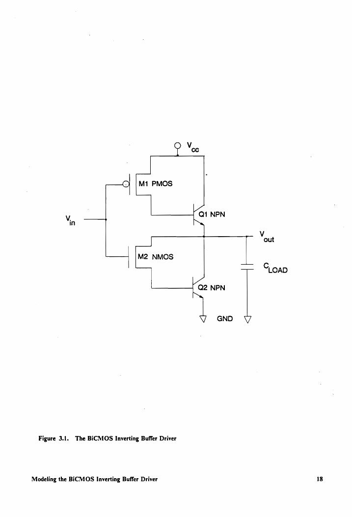
3.2 The BiCMOS Inverting Buffer Driver
The basic BiCMOS inverting buffer driver configuration is shown in Figure 3.1. It
consists of four transistors - a PMOS, an NMOS and two bipolar NPN devices. These
are marked in the figure. The operation of this inverter can be explained in the following
manner. A high to low pulse at the input will cause the PMOS device (M1) to turn on
and drive the base of the NPN transistor QI] which is initially off: This base drive will
eventually switch QI on and the load capacitance C, will be charged to a voltage V., -
V;0n). The output is constrained from reaching V.. by the base-emitter drop of QI.
This represents the output rise characteristic. When there is a low to high pulse at the
input, MI and consequently QI are turned off. NMOS transistor M2 is turned on and
supplies base drive to Q2. Once Q2 is turned on, the load capacitance is quickly
discharged to a voltage which is one diode drop above ground. This completes the
output fall transient.
It is clear from the above description that this BiCMOS inverter does not possess
rail to rail logic swing, 1.e., it does not swing from ground to V,, and vice versa. Both ends
of the swing are constrained by one diode drop, typically 0.7 volts. Therefore threshold
Modeling the BiCMOS Inverting Buffer Driver 17
Page 28
—? M1 PMOS
— M2 NMOS
Figure 3.1. The BiCMOS Inverting Buffer Driver
Modeling the BiCMOS Inverting Buffer Driver
Q1 NPN
V out
— Soap
Q2 NPN
GND V7
18
Page 29
voltages of the MOS devices must be closely monitored so that unwanted switching does
not occur. An obvious advantage of this type of inverter is the high input impedance
provided by the MOS devices and the low output impedance due to the BJTs. This
results in good input-output isolation and drive capability. Hence the name “BiCMOS
Inverting Buffer Driver”. We are now in a position to analyze the rise and fall transients
independently.
3.3 Output Rise Characteristic Analysis
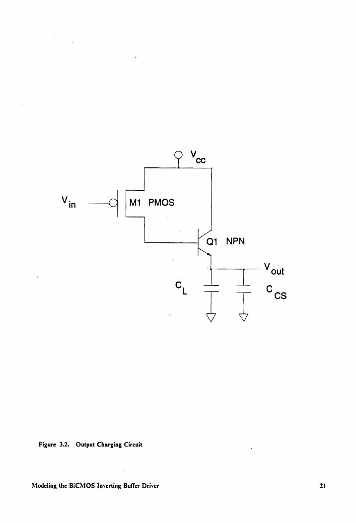
We have already seen in the preceding section that the two devices responsible for
the output rise characteristic are M1 and QI. This subsection of the inverter is shown
in Fig. 3.2 along with the external load capacitance coupled in parallel with the collector
to substrate capacitance of Q2. For this analysis, we assume that both devices are off
initially and V,,, is zero. Now, a sharp high to low pulse is applied at V,. M1 is turned
on and enters the saturation region. A constant drain current feeds the base of QI, which
remains off until the base emitter voltage Vs(on) is reached at the base node. We denote
the time at which this occurs as 4. Once QI] is “on”, it begins to supply current to the
load capacitance C,. The charging of C,+ Cs results in a rise in the output voltage
Vue When Voy reaches a certain voltage, M1 moves into the linear region. We denote
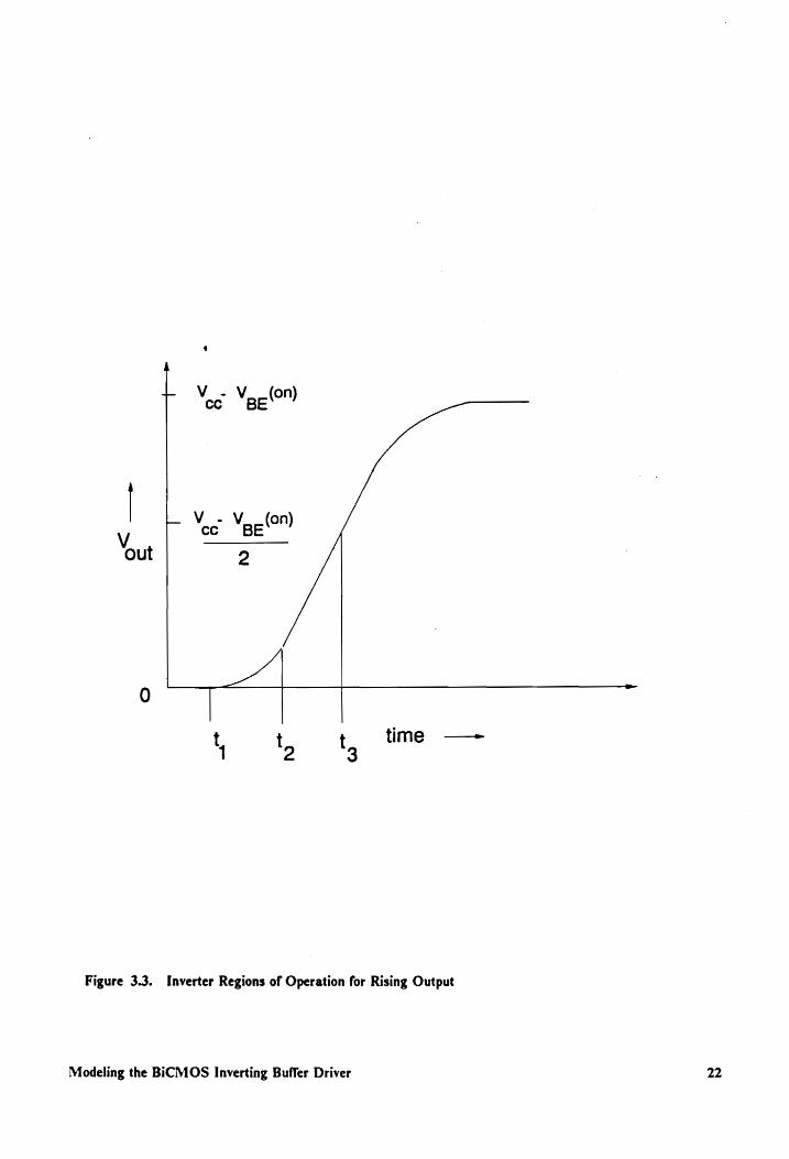
the time of this occurrence as #,. Since switching delay is of primary importance in this
analysis, a third region whose upper limit is set by the time it takes for V4. to reach
(Vee — Vaz(on) )/2, taken as the approximate switching point, is considered. This time is
Modeling the BiCMOS Inverting Buffer Driver 19
Page 30
denoted as &. These regions of operation are shown in Figure 3.3. We now consider each
of these regions individually.
3.3.1 Region 1
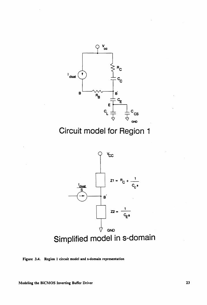
This region is characterized by M1 operating in saturation and QI! in the cutoff
region. The current supplied by M1 is modeled by a single current source denoted by
Tact Q1 is:modeled by a base resistance Rg, collector resistance Re, collector capacitance
Cc and an emitter capacitance Cz in series with the net output capacitance C,+ Ccs. The
composite circuit model is shown in Figure 3.4a. Normally, C,+Ccs is much greater
than C;. Therefore the voltage at node B’ is effectively the drop across Cz. In order to
derive an expression for Vs, we need to convert the circuit elements into frequency
domain impedances and then use inverse Laplace transforms to arrive at relationships
in the time domain. The circuit as configured in the s-domain 1s shown in Figure 3.4b.
The steps leading to the derivation of an expression for Vs; are worked in Appendix A.
The expression for Vz as derived in Appendix A is of the form,
Licart C 2 —f
Vel) = Goce t laa Se) Ul - ex] (3.1)
where
Modeling the BiCMOS Inverting Buffer Driver 20
Page 31
© Yee
Vin — M1 PMOS
{a NPN
Figure 3.2. Output Charging Circuit
Modeling the BiCMOS Inverting Buffer Driver
V out
“cs
21
Page 32
Vout
+- Vee V___(on) BE
paeen Vv. cc Vig 0")
Figure 3.3.
t t t. time —-
Inverter Regions of Operation for Rising Output
Modeling the BiCMOS Inverting Buffer Driver 22
Page 33
Os
| GNO
Simplified model in s-domain
Figure 3.4. Region | circuit model and s-domain representation
Modeling the BiCMOS Inverting Buffer Driver 23
Page 34
Wye Tasae= pp (Vee = |V) (3.2)
u is the mobility, « is the permittivity, ¢,, is the oxide thickness, W is the gate width, L
is the gate length, V,, is the supply voltage and V; is the MOS threshold voltage. And,
the term ¢ is of the form,
— ReCgCe "Cet Ce (3.3)
Typically, t is much greater than t so the exponential term in (3.1) can be neglected.
Time delay 4, is calculated by setting V;(t) = VsAon). The resulting expression for & 1s
Vpe(on) RCo
net COT Cet Co (3.4)
The effective output voltage in region | is zero since, as mentioned earlier, C, + Ccs > >
C;. The total delay in this region, which is also the time it takes for QI to turn on, is
given by (3.4).
Modeling the BiCMOS Inverting Buffer Driver 24
Page 35
3.3.2 Region 2
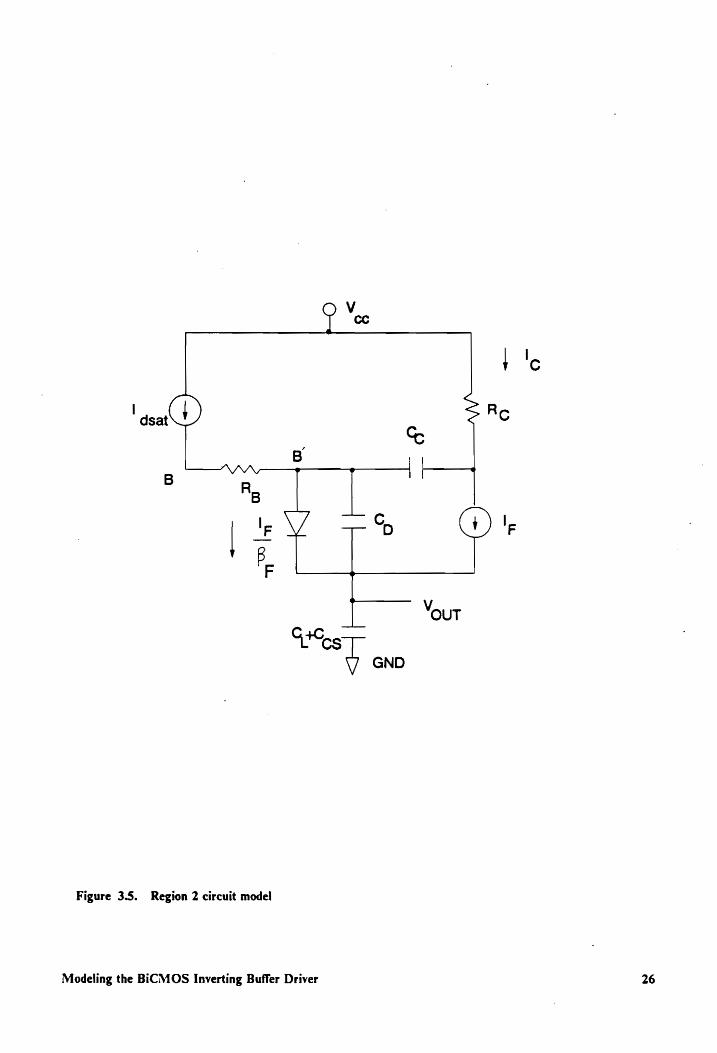
This region is characterized by M1 remaining in the saturation region and QI in the
“on” state. The complete circuit model is shown in Figure 3.5. Cp is the base emitter
diffusion capacitance. Since Vsg can be approximated by Vs(on) which is assumed to
be constant, Cz can be neglected since
Summing currents around the loop, we can write the following expression for the
current flowing into the base of QI:
Tee eg CE CL Vet LR VV. 3.5 dsat =F - Dar + cop Veet lcRe + our ~ Vcc) (3.5)
where
r ={-— 4
and
qV.
Ip= 1, exp(—=*) (3.6)
which is the standard diode current relation. /, is the saturation current, q is the
electronic charge, k is the Boltzmann constant and T is the absolute temperature.
Modeling the BiCMOS Inverting Buffer Driver 25
Page 36
a
1 'o
‘asa 1) om Re
ran, __®B |
se mel if 7? F La
Figure 3.S. Region 2 circuit model
Modeling the BiCMOS Inverting Buffer Driver 26
Page 37
The base-emitter diffusion capacitance is given by [27] :
AQng — Atel ec) CO= Wag Ware (3.7)
Now Ice is approximately equal to J; so after differentiating according to (3.7) and
simplifying we have
q Co= Uy tr (3.8)
where t; 1s the forward base transit time.
We know that when compared to V..,, Vse is constant. Therefore the differential term
involving Vg-z in (3.5) can be set to zero.
Also, since C,+Ccs > > Ce, we can consider Jc as being equal to /; and for standard
values of B, Ie = Ic. Hence,
qV. dV Ip= I(T) = (Ces + CO (3.9)
(3.5) can be written as
Modeling the BiCMOS Inverting Buffer Driver 27
Page 38
_;_l Ce qtr RCo WV yg Tasa=(Bo+ eS, ter tae ae
Differentiating the expression for J, in (3.9) we get
diy q_ AW yg dt’ KT sar
The expression for Jz. can then be rewritten as
1 + dl, fasoe =e tet
where
11, Bo Br Cost Cy
and
r =Tr + RcCe
Solving differential equation (3.11) we get
IAC) = B Tasaill — exp m —)] tT
Modeling the BiCMOS Inverting Buffer Driver
(3.10)
(3.11)
28
Page 39
Using this expression in (3.6) we get
AV out B' Lasat —f
ad’ Cos tC, et CxPC oe )] (3.12)
Integrating (3.12) with respect to ? and noting V,,, is zero when r = 0, we have
B ° I dsat v
= 3.13 Bt ))} (3.13) Voudt’) = {r — B'c'(1 — exp(
Since M1 is still in saturation, the expression for J. is the same as in (3.2). The end of
region 2 which is marked by 4, is the time at which M1 comes out of saturation. This
occurs when the gate to drain voltage of M1 is greater than the threshold 1.e. when
Vour = |Vrl — Vag(on)
since the input voltage is zero.
We have to plug this value into (3.12) and solve for ’. To do this we have to simplify
(3.12) by expanding the exponential term in a Taylor’s series. This is possible since ’’ is
normally << rt’. We retain terms up to the second degree, simplify and obtain a
quadratic equation with the solution,
c= Jia + Ces) (IV — Vegton)) (3.14) I dsat
Modeling the BiCMOS Inverting Buffer Driver 29
Page 40
The Taylor’s series simplification is explained in Appendix A. Since ¢’ = t, - h, we have
an expression for the delay between the time QI turns on and M1 enters the linear
region. The total delay at the end of Region 2 is the sum of delays indicated by equations
(3.4) and (3.14).
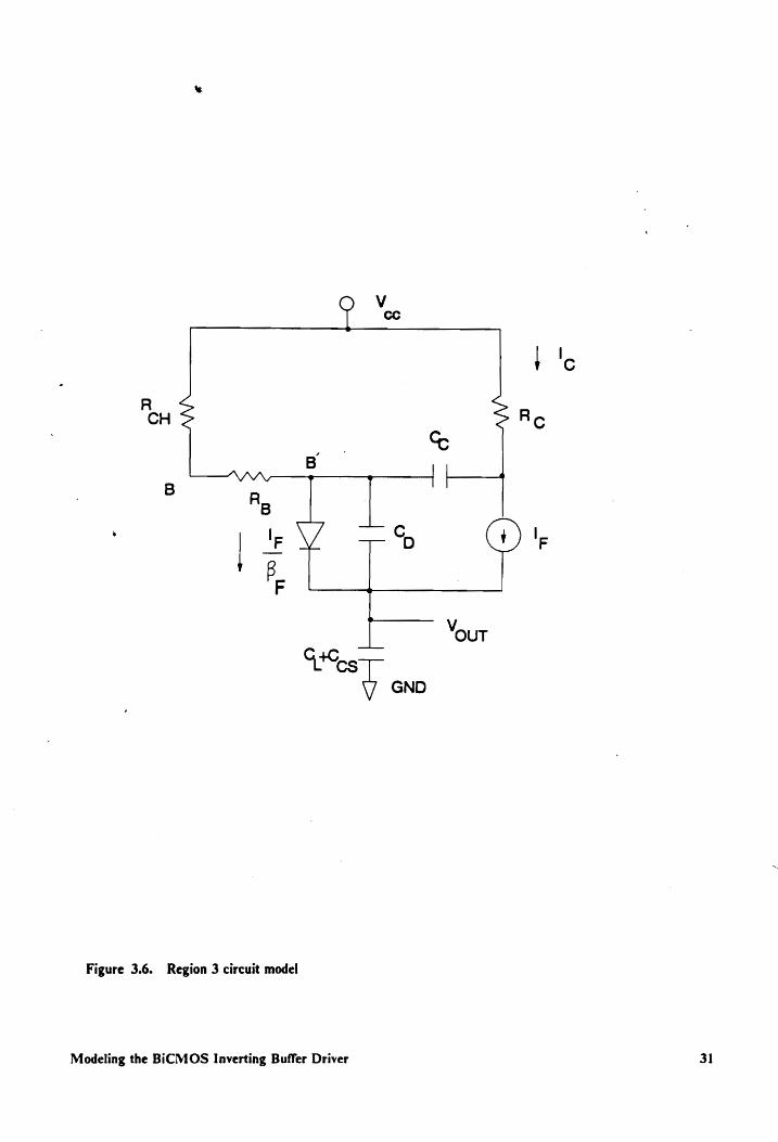
3.3.3 Region 3
In this region M1 has just moved out of saturation into the linear mode while Q1
remains “on”. So, the only difference from the model in Region 2 is that M1 is
represented by a channel resistance instead of a current source. The complete model is
shown in Figure 3.6. We can write the following expression for the current flowing into
the base of QI:
Voo— Vere — Vout I; = Ray t Ry (3.15)
Ft, oe cd (Varg t IcRe+ Vout — Veo) Br D dt’ C "ar BE cc out "CC
Here, f’ = t- hy.
Using the same assumptions as in the Region 2 analysis, we can write for (3.15):
Modeling the BiCMOS Inverting Buffer Driver 30
Page 41
R wd Re
| %
BR . q + | |
\ |< _— & le
F
Figure 3.6. Region 3 circuit model
Modeling the BiCMOS Inverting Buffer Driver 31
Page 42
Fi ql; AV yg Vout AV out Voc ~ Veeg
+oep rt RCo + ROR, + oo Gp) = Rae, (3.16)
pr AT
We assume that Veg = Vez (on). Further, we differentiate (3.9) to obtain
2 ql AV pp d Vout
We can now rewrite (3.16) as
2 te a Vou + 1 Woy + Vout Voc — Vaz(on) (3.18)
(dry pp a (Rew + Ra)\Cost Cy (Rew + Ra)Ces + Cy
which is a second order differential equation in V,,,. A solution to (3.18) is given by
Voudt’") = Cy exp(myt”) + Cy export”) + Veo ~ Vag(on) (3.19)
where C, and C; are constants and
)-1 (3.20)
T, is of the form,
Modeling the BiCMOS Inverting Buffer Driver 32
Page 43
Ty =./ (Rew + Rg\(Ces + Ct
T, is generally much smaller than 28° t° for commonly used device parameters.
Therefore, roots m, and m, will be negative. Note that we have dropped the F subscript
for the # and t terms, since we know that the bipolar device is operating in the forward
mode. Since the roots are negative, (3.19) wil be of the form,
Vout’) =€C sin( =) +D cos( =) exp( —+ a —) + Veco — Vgz(on) (3.21) t
where C and D are constants and
T, 2 ee ) 1—(
We now have to determine the constants C and D in (3.21). In the preceding analysis,
we have seen that at t= 4, the output voltage is given by
Vour = |\V7i — Vg-(on) (3.22)
Att= 4,’ = 0. Plugging this into (3.21) we get
Modeling the BiCMOS Inverting Buffer Driver 33
Page 44
V out = D + Vee _ Vp-(0n) (3.23)
Equating (3.22) and (3.23) we have for D:
= — (Vee — |V 7)
Differentiating (3.21) we get
WVoulto) — C D dr’ — T —_ 2p'r" (3.24)
To get another expression involving C, we differentiate (3.13) with respect to t’ and
simplify to obtain :
AV dt) ~ lasakt ~~ f) —-> : (3.25)
dr’ Cost Cyt
We now equate (3.24) and (3.25) and solve for C, after plugging in the expression for
T. The final equation for C is
D T, p2 Ren t+ Rg . (Vr — Vee(on) | C= — 2 3.26
J1—-(T,/26't 2p ( Rex Vee —\Vr TY 626)
Modeling the BiCMOS Inverting Buffer Driver 34
Page 45
Terms inside the square brackets of (3.26) are typically < < 1. So, the magnitude of C
will be much smaller than that of D. Hence, we can neglect C in the expression for Viu
which is now simplified to
Vouk") = (Veo |W rI)L1 ~ cos( ==) exp — "/28°r")] + [Vel — Vaglon) (3.27)
Equation (3.27) represents the final V,,, expression for Region 3. The time delay can be
obtained by approximating the exponential term in (3.27) by unity and setting V., =
(V.. - Vase (on))/2 which is the 50% rise mark. The time delay can now be written as
Veco — Vag(on) ~w ~i ~ Veo = |W) }~Tcos (0.5)~T (3.28) f'=h-—bh~T cos{
The total 50 % delay is obtained by summing up delays for each of the three regions.
Hence,
tg = te te" (3.29)
This completes the Region 3 analysis. Expressions for the output voltage and total delay
up to the 50% rise mark have been derived. In the next section the effect of bipolar
device saturation on the delay will be discussed.
Modeling the BICMOS Inverting Buffer Driver 35
Page 46
3.3.4 Collector Saturation
The previous discussions assumed that QI remains in the linear region throughout
Region 3 operation. However, for moderate values of load capacitance and collector
resistance, QI can operate in the collector saturation region. Under such conditions, the
following equation may be written for the drop across the collector resistance :
LAtsa)Re = Vee ” Vep(sat) - Vourltsar) (3.30)
where ¢,. is the time in Region 3 when collector saturation occurs. Since Ic = Je we can
write
dV, I¢= (Ces + C= (3.31)
Differentiating (3.27) and using the result in (3.31) we get
nv Mest CO Vcco— Vr). or’ r’ I(t’) = 77 sin( > ) exp(- —>7) (3.32)
28 t
Substituting (3.32) and (3.27) into (3.30) gives
Rd Cest Cy). beat Usar Vp(on) — Vef(sat) bsar ———— sin( ——- ) = cos + exp( —> 3.33 s (pr) = 008) + EF yg See) (3.33)
Modeling the BiCMOS Inverting Buffer Driver 36
Page 47
For typical device parameters, the exponential term on the right hand side of (3.33) is
- approximately I and its multiplier is < < 1. Hence, we can neglect this term and arrive
at the following expression for te :
T
tae TBR FED (3.34)
The expression for output voltage after saturation has occured, can be obtained by
replacing the denominator of the exponential term argument in (3.27) by R{Cz + Ces)
to indicate the dominance of the load capacitance and collector resistance in the
response. /,, represents the “post saturation” delay.
— f ¢
Voullgs) = (Veo — WW el)L1 — cos( 22) exp\ RiGopt G) UtIVA-Vaelon) (3.35)
The value of the output voltage at saturation is obtained by setting 4, = 0 in (3.35)
t Voud tsar) ¥ Veo — Vgg(on) — (Veco —\Vr}{1 — cos *)] (3.36)
The effect of saturation on the gate delay can be accounted for by including ¢,., in the
delay calculations. Total delay at saturation is calculated by adding 4, 7 and ty,
Modeling the BiCMOS Inverting Buffer Driver 37
Page 48
3.4 Results and Comparison with SPICE Simulations
The equations derived in the previous sections have been programmed and a
composite curve for the output response has been plotted in Figure 3.12. This is to be
compared with results obtained from SPICE simulations. PSPICE 3.04 running on a
80386 based IBM-PC has been determined to be quick and accurate enough for this
study [1].
The MOS device dimensions used for this study are the same for N and P devices -
a width of 30um and length 2um. Unit sized bipolar transistors are used and the load
capacitance value is 5pF. In the PSPICE simulations, the Shichman-Hodges model is
used for the MOS devices while a simplified Gummel-Poon model is used for the NPN
transistors [27]. A list of principal MOS and NPN device parameters used, is provided
on the following pages. We are assuming that high level injection effects do not occur
in the bipolar transistors since only moderate collector resistance values are assumed.
For the PSPICE deck we set the knee current to its default value of infinity to ensure
this.
Modeling the BiCMOS Inverting Buffer Driver 38
Page 49
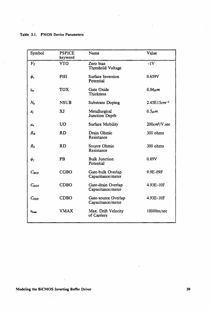
Table 3.1. PMOS Device Parameters
Symbol PSPICE Name Value keyword
Vr VTO Zero bias -1V Threshold Voltage
o: PHI Surface Inversion 0.659V Potential
lox TOX Gate Oxide 0.04: Thickness
Ny NSUB Substrate Doping 2.45E1Sem-3
x XJ Metallurgical 0.5m Junction Depth
He UO Surface Mobility 200cm?/V.sec
Rp RD Drain Ohmic 300 ohms Resistance
Rs RD Source Ohmic 300 ohms Resistance
$; PB Bulk Junction 0.89V Potential
Caco CGBO Gate-bulk Overlap 9.9E-09F Capacitance/meter
Coco CDBO Gate-drain Overlap 4.93E-10F Capacitance/meter
Csco CDBO Gate-source Overlap 4.93E-10F Capacitance/meter
Vmax VMAX Max. Drift Velocity 10000m/sec of Carners
Modeling the BiCMOS Inverting Buffer Driver 39
Page 50
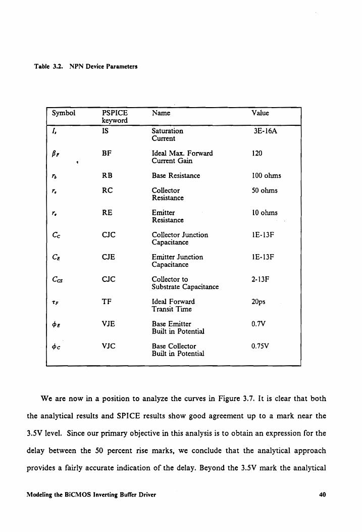
Table 3.2. NPN Device Parameters
Symbol PSPICE Name Value keyword
L IS Saturation 3E-16A Current
Br BF Ideal Max. Forward 120 Current Gain
lb RB Base Resistance 100 ohms
Te RC Collector 50 ohms Resistance
le RE Emitter 10 ohms Resistance
Ce CIC Collector Junction 1E-13F Capacitance
Cz CJE Emitter Junction 1E-13F Capacitance
Ces CIC Collector to 2-13F Substrate Capacitance
tr TF Ideal Forward 20ps Transit Time
de VJE Base Emitter 0.7V Built in Potential
dc | VIC Base Collector 0.75V Built in Potential
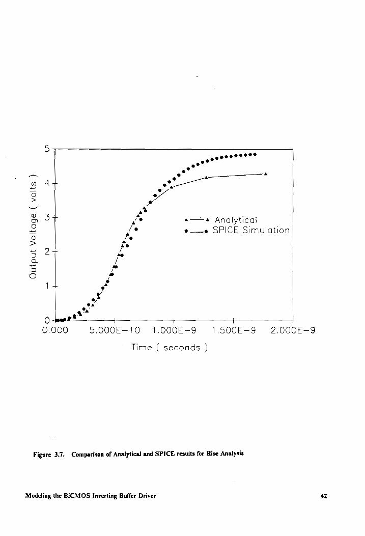
We are now in a position to analyze the curves in Figure 3.7. It is clear that both
the analytical results and SPICE results show good agreement up to a mark near the
3.5V level. Since our primary objective in this analysis is to obtain an expression for the
delay between the 50 percent rise marks, we conclude that the analytical approach
provides a fairly accurate indication of the delay. Beyond the 3.5V mark the analytical
Modeling the BiCMOS Inverting Buffer Driver 40
Page 51
curve approaches the 4.3V mark asymptotically while the SPICE curve continues on
before doing the same, close to the 4.85V mark. The reason for this difference can be
explained as follows :
Throughout the analytical modeling process, we have assumed that the base-emitter
drop of the bipolar transistor remains constant i.e. at Vs:(on) taken as 0.7V. In actual
practice, this drop is not constant and is related to the collector current by the following
expression :
Io = If exp( *))
Therefore, as the collector current becomes smaller, the base-emitter drop is also
‘reduced. At the end of the collector saturation region the collector current is very small
and hence, Vz is also greatly reduced from 0.7V. The expression that SPICE uses to
relate J¢ to Vee is very complex and has to be computed iteratively. Our objective with
the analytical approach 1s to arrive at the simplest possible closed form expression which
can provide a reasonable first approximation for the delay. As mentioned before, the
equations derived are able to do this. In addition, it must be noted that the times at
which both curves approach their final values are similar, so the overall rise times for
both will be quite close to one another in value. We conclude therefore, that the
equations for delay calculations can definitely be used for first approximations, while
keeping in mind the actual voltage levels achieved.
Theoretically, one way to improve the predicted voltage levels by taking into
account the Vz variation would be to factor results of experimental or simulated data
into the analytical equations. Appendix A details how this would constrain the
simplicity and closed form nature of these equations.
Modeling the BiCMOS Inverting Buffer Driver 4l
Page 52
gooodccceee® e® e°
o™~ e en
v 44 oo
9 we ‘oO a* oT ° a——a Analytical
a /@ ee SPICE Simulation © /@
> se ~ 24 /
a r°
3 S 14 s
@
ot
@a
Pt 0 -wese 4 _4 1
0.000 S.QQOOE-10 1.000E-9 1.500E-9 2.Q000E-9
Time ( seconds )
Figure 3.7. Comparison of Analytical and SPICE results for Rise Analysis
Modeling the BiCMOS Inverting Buffer Driver
Page 53
Having completed-the inverter output rise analysis, we now undertake a similar
approach towards the output fall analysis. It must be noted that the fall analysis is
equally important, because it allows us to gauge the total delay through the gate.
3.5 Output Fall Characteristic Analysis
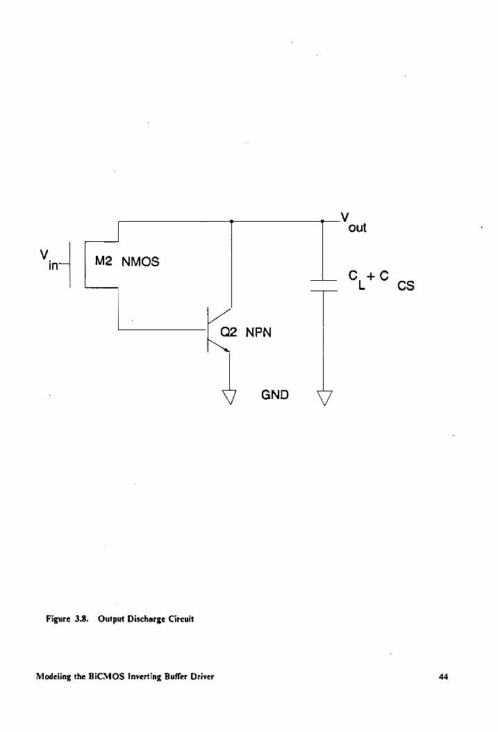
In this section the high to low output transient will be analyzed. We assume that
the output is already at logic 1’ and a sharp positive transition occurs at the input. The
devices that are responsible for this operation are shown in Figure 3.8. When V,, goes
high, NMOS device M1 is turned on and it begins to source current to the Q2 base. Q2
turns on after the base-emitter threshold voltage is reached and speeds up discharge of
the load capacitance. The final output voltage is one diode drop above ground. Just as
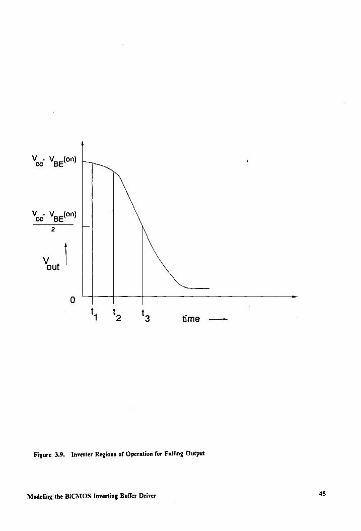
in the rise analysis, we can divide this operation into three regions in time. Initially, M1
is in saturation and QI is off. At time 4, QI turns on. M1 remains in saturation until
time ¢, after which it moves into the linear region while QI] remains on. We consider a
third region bounded by the time at which the downward output transition crosses the
Viigs/2 mark, considered to be the approximate switching point. The three regions
characterizing this transient are shown in Figure 3.9. We shall now undertake a detailed
analysis of these regions of operation.
Modeling the BiCMOS Inverting Buffer Driver 43
Page 54
V > M2 NMOS
Figure 3.8. Output Discharge Circuit
c NPN
wo
Modeling the BiCMOS Inverting Buffer Driver
out
C L* © og
44
Page 55
‘oe Viggo") = ‘
‘oe Vpe(on) 2 _
Mout
NO
0 =
t t 1 ‘2 ', time —-
Figure 3.9. Inverter Regions of Operation for Falling Output
Modeling the BiCMOS Inverting Buffer Driver 45
Page 56
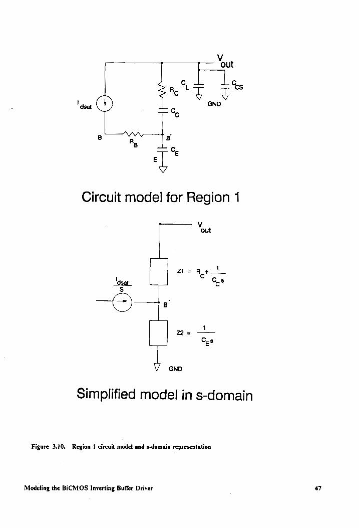
3.5.1 Region 1
In this region M1 is in saturation and QI is off. The circuit model is shown in Figure
3.10a. Since the load is being discharged only by the MOS device, we can write :
dV, Cour 7 ~ — lesat (3.37)
where C,., is the composite load capacitance comprising of the external load plus the
collector to substrate capacitance. Integrating (3.36) we get
I . a t+K (3.38)
out
Vour =
where K is a constant which may be determined by noting that at t=0 the output
voltage is Vcc - Vson). The final expression for Vu, is
I Vour = — a t+ Veo — Vgg(on) (3.39)
oul
To calculate the delay we have to derive an expression for the voltage at B’ since we
know that the boundary of Region 1 is determined by the time at which the voltage at
B’ is Vs{0n). Essentially, the expression is derived in Appendix A. The simplified circuit
in terms of s-domain impedances used for this analysis appears in Figure 3.10b. The
expression for V» is
Modeling the BiCMOS Inverting Buffer Driver 46
Page 57
Zi=A+_! lsat C.8
S -O-f. 1
22=
Ces
GND
Simplified model in s-domain
Figure 3.10. Region 1 circuit model and s-domain representation
Modeling the BiCMOS Inverting Buffer Driver 47
Page 58
Lis 2 V(t) = tt + Nasa HE) + 3.40 BO) = CC, t Masa Ce) UL explo) (3.40)
In 3.40, the drain current is given by
Wye Masa = Fy Veo ~ Wel) (3.41)
t has already been defined in (3.3). The time 4 at which Q2 turns on is obtained by
solving (3.40) for t, with Vs (t) = Vesdon):
Vae(on) — ReCe" Tasat CetCe
This completes the Region | analysis. The total delay up to this point is 4. We now
perform the analysis for Region 2.
3.5.2 Region 2
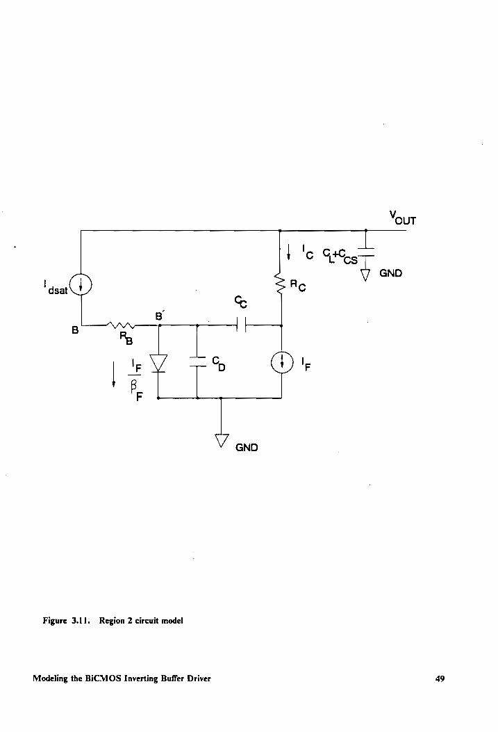
M2 operates in saturation while Q2 is “on” in this region. The complete circuit
model is shown in Figure 3.11. We are assuming a constant base- emitter voltage so we
neglect the emitter capacitance. From Figure 3.10 we can write the following current
equation :
Modeling the BiCMOS Inverting Buffer Driver 43
Page 59
& B ||
B “AAV 1 |
Fe —__
jr¥ 78 B ;
GNO
Figure 3.11. Region 2 circuit model
Modeling the BiCMOS Inverting Buffer Driver 49
Page 60
dV out Cour de = — (Lasar + Ic) (3.43)
where 7?’ is the time elapsed since the end of Region I. The following relation for the
drain current can be written :
Fe dV pp lssat = Br + Cp = + Coa £ (Veg + IcRe — Vous) (3.44)
The Vs, term in the expression within parentheses can be neglected since we are
assuming a constant base-emitter drop. Also we may safely assume that [7 = I;
following the path of near zero impedance.
The following relations for terms in the above equation are reproduced for the sake of
continuity :
qV eve Ip = 1, exp( kT ) (3.6)
dlr =] _F aye d’ F KT dr’
Cyacerl (3.8) D™~ kT F*F .
Modeling the BiCMOS Inverting Buffer Driver 50
Page 61
Using these equations, the expression in (3.44) can be simplified in the following manner,
I q dV» lesa = G+ (t+ RCO EE ap le - Ce
_ Tr acy fle Mout = tt cCo) ad’ © dr
Ir «dlp dV oun Bet ae oar
Using (3.43) we can rewrite (3.46) as
Ip «dlp C wey Ae So lasat = Br + dt’ Cour (Lasar + Ic)
Since I; ~J;, we can write :
Cour - Ce IF « dl, ( Cout ) Lasar = gs + dr
where
Modeling the BiCMOS Inverting Buffer Driver
(3.45)
(3.46)
(3.47)
(3.48)
SI
Page 62
l l Cec == +—-
B Br Cour
and
co=tt+ RoCe
(3.48) is a differential equation with the following solution :
Cout ~
* Ce —t IA’) = 8 (—~“E_ Masat [1 — exp( > )] (3.49)
out Br
From (3.43) and since Jc ~ J, (3.49) can be written as
AV out lasat . (Cour ~~ Co) —f —~ = -— [1 + 8 a (1 - ex = 3.50 at Co, [1+ C., ( p( Bt J (3.50)
An expression for V,,, can be derived by integrating (3.50) with respect to time. For ¢’
= 0, f= 4%, which can be calculated from (3.42), and then (3.39) can be used to calculate
Vue at this point in time.
On integrating (3.50) we get
Modeling the BiCMOS Inverting Buffer Driver 52
Page 63
=! yds K © (3.51)
I © (Con C oe Vault) = — Ete +p SoS) oe 4. Bo" exp( = out out Tt
K is a constant which can be calculated by plugging the value of V,,, calculated from
(3.39) into (3.51), keeping ¢’ zero. We assume for the sake of brevity that K is equal to
fVcc, where fis a number between 0 and 1. The final expression for V.,, in Region 2 is
Losat © (Cur—C a Vault) = ~2EUe +p Kou C2 + Bt x S514 Ice (3.52)
The drain current is given by
W pe lasae= Zp, (Vee [Vik — Vse(om)y"
This region is bounded by the time at which M1 comes out of saturation, i.e. when
Vour=SVcc — Vr t+ Veg(on) (3.53)
We substitute the above value of V,,, in (3.52) and expand the exponential term in (3.52)
in a Taylor’s series. After retaining terms up to the second degree and simplifying, we
get a quadratic equation in ’’. This may be solved to yield the following expression :
Modeling the BiCMOS Inverting Buffer Driver 53
Page 64
4 Cour
—1+ J1- + (Vpg(on) — |V7)) Tt
f=h-t= IF (3.54)
This is an expression for the delay in Region 2. The total delay at the end of this region
is obtained by summing the delays predicted by (3.42) and (3.54). Next, the analysis for
Region 3 is performed.
3.5.3 Region 3
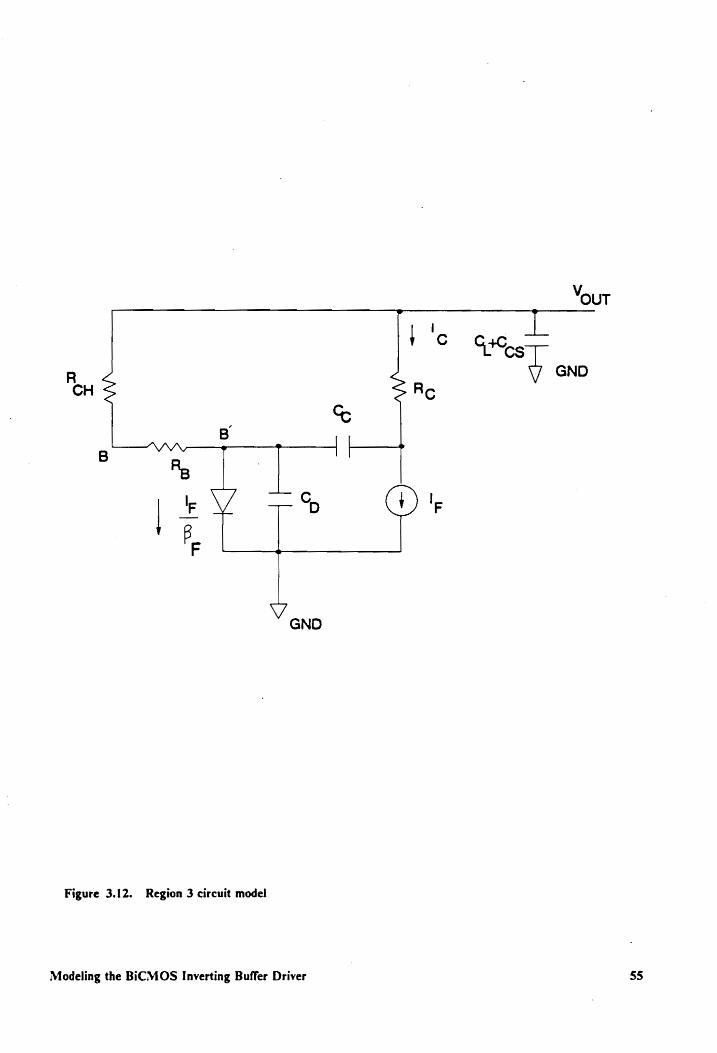
M2 moves into the linear mode while Q2 stays “on” in this region. The complete
circuit model is shown in Figure 3.12. We can write the following expression for the
current flowing into the base of Q2:
Vout ~~ Vive fp= ent
(3.55)
=3- + Cpa + Comer Vag + IcRe — Vous)
where ’’ = ¢— 4, and other terms are as per earlier definitions. Once again, since we are
assuming a constant base-emitter drop, the differential of the V;, term in parentheses
is negligible relative to that of V,,,. Also, we substitute for Cp from (3.8) to get
Modeling the BiCMOS Inverting Buffer Driver 54
Page 65
OUT
G+C
= S : Ro eb GND
GND
Figure 3.12. Region 3 circuit model
Modeling the BiCMOS Inverting Buffer Driver
Page 66
AV yg AV out
caer TR Comer I q In= i + (t+ ReC) Te (3.56)
Now,
dV. rf) + I¢ = Cour a
i.e.
Vour 7 Vee d Vout Rent Ry tle™ ~S (3.57) out dt’
since [ry = Ic. Differentiating (3.57) with respect to r’’ we have
1 dV ~ ~(C dV out _ 1 AV out
kT F de’ oul iy? (Rey +R) dt’ (3.58)
Substituting for the expression on the left hand side of (3.58) in (3.56) and simplifying
we get
DV on AL Mout Vout _ Vpp(on) 3.59)
dr’? gt dt” (Rew + Rg) Cour (Rew + Re) Cour Tt
Modeling the BiCMOS Inverting Buffer Driver 56
Page 67
where
t =Tr + RCo
1 Ce l r ; +--+ B | Count Bp CoudRew + Re)”
(3.59) is a second order differential equation in V,,,. Its solution is of the form,
Voudt’’) = Cy exp(mmt’’) + Cy exp(m,r’’) + Vgg(on) (3.60)
where C, and C, are constants and
)-1 (3.61)
where
Ty = \/ (Ren + Re)(Cos + Cpt
For standard device parameters, sm, and m, will be negative so the expression for V,,, will
be of the form,
Modeling the BiCMOS Inverting Buffer Driver 57
Page 68
Voudt’’) =[C sin( =) +D cos( -S- =] exp( — 7 ; —) + Vp,(on) (3.62) t
where C and D are constants and
To determine values of C and D we perform the following steps. From (3.62) we know
that att” = 0,
V out = D+ Vp e(on) (3.63)
From the Region 2 analysis we know that at t= h,
Vout =o — Vr + Vee(on) (3.64)
Equating (3.63) and (3.64) we have
D = fVec—|V7
Now, by differentiating (3.62) and setting t” = 0 we get
Modeling the BiCMOS Inverting Buffer Driver 58
Page 69
dV out ( C D ar’ =O) = re
Further, we also differentiate (3.52) with respect to t’ and simplify to obtain
fae St (p’) = — SL Lasat (1 + r j
Cour T
Now, at t= 4, f is given by (3.54) so we can write
AV ous Lasat dsat™
4 Cour “1+ fi- £ (Vgg(on) — [Vrl)
Equating (3.65) and (3.66) we get
4 Cout —l+ J _ = (Vg¢(on) — |V 7)
dsatt Lasat C= T —T —— [l + ] (S 5
(3.65)
(3.66)
(3.67)
For typical device parameters we find from (3.67) that C < < D. Hence, (3.62) can be
simplified to
Voudt’ )= D cos( =) exp( —> * 2 =) + Vpg(on) a t
Modeling the BiCMOS Inverting Buffer Driver
(3.68)
59
Page 70
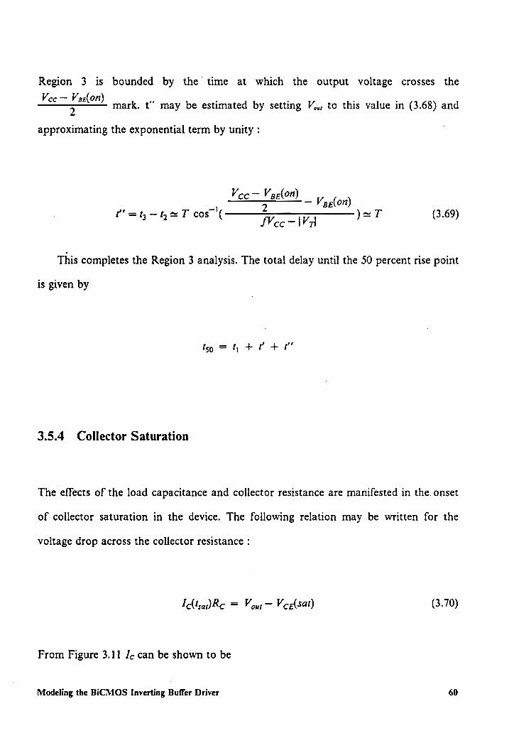
Region 3 is bounded by the time at which the output voltage crosses the
Vee — V5e(0n)
2
approximating the exponential term by unity :
mark. t’” may be estimated by setting V,., to this value in (3.68) and
Veo — Vae(on) 2
Veeo- Wr
— Vgz(on) t'=t;-t,~T cos” )=T (3.69)
This completes the Region 3 analysis. The total delay until the 50 percent rise point
is given by
b= terete’
3.5.4 Collector Saturation
The effects of the load capacitance and collector resistance are manifested in the. onset
of collector saturation in the device. The following relation may be written for the
voltage drop across the collector resistance :
IAtsa)Re = Vour— Vce(sat) (3.70)
From Figure 3.11 J~ can be shown to be
Modeling the BiCMOS Inverting Buffer Driver 60
Page 71
dV. le= — (Cou 2 + Ip)
Differentiating (3.68) and neglecting the smaller terms we have
Again, from the circuit model, the base current can be written as
Vour — Vpe(on)
I, = Rey + Rg
From (3.70) through (3.73) we are able to write the following :
Dt =r" D r” =r! lo = Coup Sin(“F ) expe) — RoR, CO F) exPls ae )
1. r! =r’ Vpe(on) = ——[Dcos({——) ex sw) + — Vo,(sat Re [ ( T ) p( 2p : ) Rey + Rp cE )]
(3.71)
(3.72)
(3.73)
(3.74)
We simplify (3.74) by neglecting the second terms of each of its constituent expressions
as being small relative to the first terms. After further simplification we have the
following expression for the time at which saturation occurs :
Modeling the BiCMOS Inverting Buffer Driver 61
Page 72
T
Courke
tear =~ T tan™'( ) (3.75)
The expression for the output voltage is derived by using (3.68) as the basis and making
appropriate changes to the arguments of the exponential and cosine term arguments to
reflect the onset of saturation and the dominance of Reand C,,, in the post saturation
response.
beat ~~ bs 7) exP(Re— 1+ Vector) (3.76)
Vourllys) = Vee —| Vy)C1 — cos(
where ¢,, denotes the delay after saturation is reached.
The output voltage at saturation can be calculated from (3.76) by setting 4, = 0:
t.
r ) + Vgze(on) (3.77)
Vourltsat) =D cos(
The total delay until the onset of saturation can be calculated by adding 4, ’’’ and trae
Modeling the BiCMOS Inverting Buffer Driver 62
Page 73
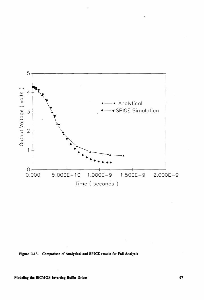
3.6 Results and Comparison with SPICE Simulations
The equations derived for the output fall response have been programmed and a
comparison with the SPICE response can be made from the curves in Figure 3.13. We
continue with the same MOS device dimensions i.e. 30um for the width and 2m for the
length. Before we analyze the results in Figure 3.13, a list of MOS and BJT parameters
used in the simulations is provided on the following pages. Once again, we are assuming
the Shichman-Hodges model for the MOSFETs and a simplified Gummel-Poon Model
for the BJTs. High level effects for the bipolar transistors are not considered since
moderate collector resistance values are assumed.
Modeling the BiCMOS Inverting Buffer Driver 63
Page 74
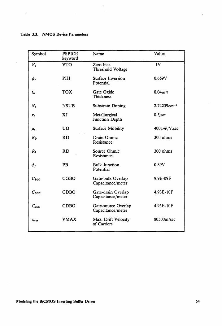
Table 3.3. NMOS Device Parameters
Symbol PSPICE Name Value keyword
Vr VTO Zero bias 1V Threshold Voltage
dy PHI Surface Inversion 0.659V Potential
tox TOX Gate Oxide 0.04: Thickness
Ns NSUB Substrate Doping 2.74259em-3
x XJ Metallurgical 0.S5um Junction Depth
Le UO Surface Mobility 400cm?/V.sec
Ro RD Drain Ohmic 300 ohms Resistance
Rs RD Source Ohmic 300 ohms Resistance
>; PB Bulk Junction 0.89V Potential
Caco CGBO Gate-bulk Overlap 9.9E-09F Capacitance/meter
Coco CDBO Gate-drain Overlap 4.93E-10F Capacitance/meter
Csco CDBO Gate-source Overlap 4.93E-10F Capacitance/meter
Vinax VMAX Max. Drift Velocity 80500m/sec of Carriers
Modeling the BICMOS Inverting Buffer Driver
Page 75
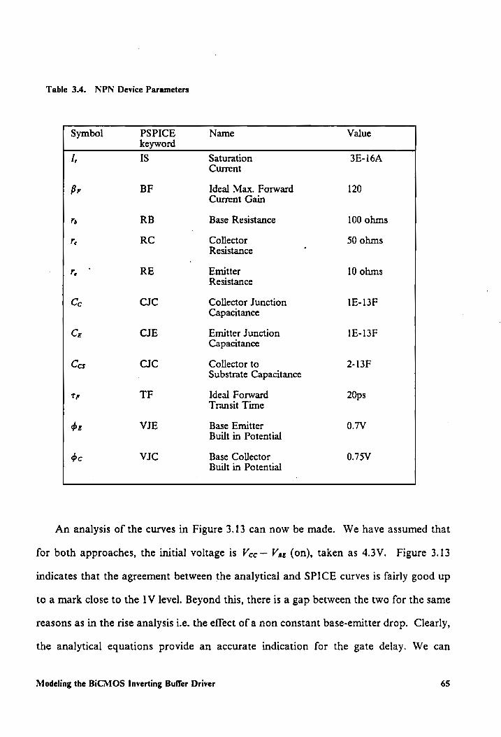
Table 3.4. NPN Device Parameters
Symbol PSPICE Name Value keyword
L, IS Saturation 3E-16A Current
Br BF Ideal Max. Forward 120 Current Gain
ls RB Base Resistance 100 ohms
le RC Collector 50 ohms Resistance
r, RE Emitter 10 ohms Resistance
Ce CIC Collector Junction 1E-13F Capacitance
Ce CIE Emitter Junction 1E-13F Capacitance
Ces CJC Collector to 2-13F Substrate Capacitance
tr TF Ideal Forward 20ps Transit Time
de VIE Base Emitter 0.7V Built in Potential
oc VIC Base Collector 0.75V Built in Potential
An analysis of the curves in Figure 3.13 can now be made. We have assumed that
for both approaches, the initial voltage is Vcc — Vag (on), taken as 4.3V. Figure 3.13
indicates that the agreement between the analytical and SPICE curves is fairly good up
to a mark close to the 1V level. Beyond this, there is a gap between the two for the same
reasons as in the rise analysis i.e. the effect of a non constant base-emitter drop. Clearly,
the analytical equations provide an accurate indication for the gate delay. We can
Modeling the BiCMOS Inverting Buffer Driver 65
Page 76
therefore use them in conjunction with the rise delay equations to predict the total gate
delay..
3.7 Summary
In this chapter, the basic BiCMOS inverting buffer driver has been modeled
analytically. The principal aim has been to arrive at a set of equations that provide an
accurate measure of the delays in this circuit. Both rise and fall output transients have
been analyzed in detail and operation of the devices is explained at length. In both the
analyses the MOS devices have been shown to be operating in the saturation and linear
regions while the bipolar devices operate in cut off and active regions. The possibility
that the bipolar devices will enter the region of collector saturation for moderately high
values of collector resistance and capacitance as well as the load capacitance, has been
discussed and elaborated upon. Under such conditions, the output response becomes
heavily dependent on the collector resistance and load capacitance values. The actual
effect of collector saturation on the output waveform has been shown - the waveform
approaches its final value asymptotically for both the rise and fall transients.
The expressions for the output voltage and time delays in each of the regions are
fairly simple and closed form in nature. Comparisons with results of PSPICE simulations
have indicated good agreement for a major part of the waveform. Reasons for deviations
at the end points of the voltage swings have been accounted for and justified in the light
of preserving the simplicity and closed form nature of the analytical approach. The most
useful end product of the analysis is the set of delay equations which allow us to make
Modeling the BiCMOS Inverting Buffer Driver 66
Page 77
nar Np Oo ‘te 2 \. 4——a Analytical
o 3+ as _ e—e SPICE Simulation
g \ i de > ee a 5 \Y © e™,
it “~~ e ° oa
% ee cee
O _t _—_| \ 0.000 S.00O0E-10 1.000E-9 1.500E-9 2.Q000E-9
Time ( seconds )
Figure 3.13. Comparison of Analytical and SPICE results for Fall Analysis
Modeling the BiCMOS Inverting Buffer Driver 67
Page 78
a first approximation of the total gate delay through the inverting buffer. These are
measured at 50 percent of the total voltage swing and are in good agreement with the
delays predicted by SPICE. The delay equations also provide information on which
circuit, MOS and bipolar parameters need to be optimized to minimize the gate delay.
With this knowledge, detailed simulations can be used to further fine tune the
optimization process. To sum up, the analytical approach affords us valuable insights
into the working of the BiCMOS inverting buffer - these could be a useful tool towards
achieving better circuit and device performance.
Modeling the BiCMOS Inverting Buffer Driver 68
Page 79
Chapter 4
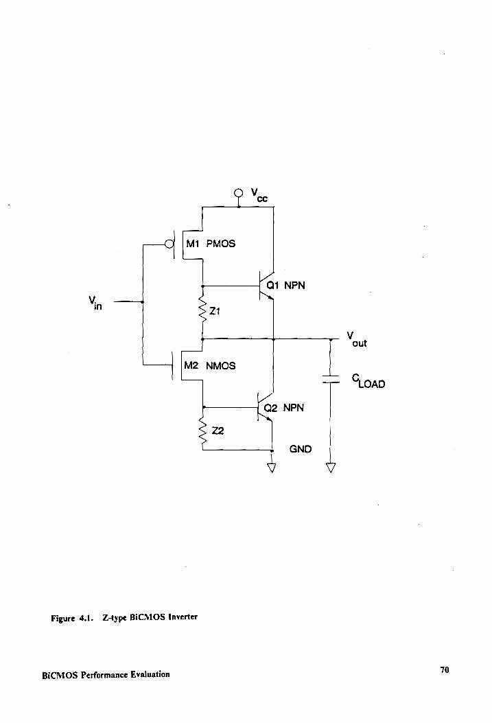
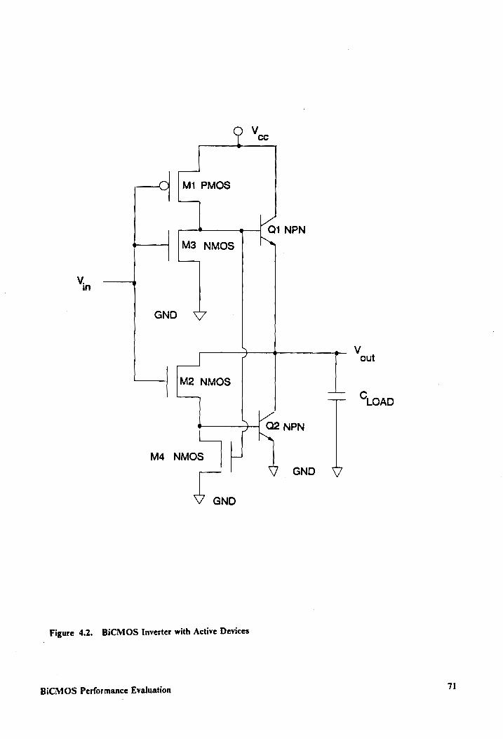
BiCMOS Performance Evaluation
4.1 Introduction
In the previous chapter the basic BiCMOS inverting buffer has been analyzed in
detail and theoretical equations allowing time delay estimates in circuits using these
devices, have been derived. Thus, an evaluation of more complex inverter configurations
is possible. There are two schemes that afford improved performance in comparison to
the basic buffer. These configurations are illustrated in Figures 4.1 and 4.2 [28].
The Z-type BiCMOS inverter shown in Figure 4.1 gets its name from the two
resistors which are present in addition to the four active devices in the simple inverting
buffer. This circuit functions in the following manner. When the load capacitance is
being charged, we have seen that the output is constrained from reaching Vcc by the
drop across the base-emitter junction of QI. In the Z-type inverter, Zl continues to
supply current to the load after the active devices have been turned off, until the output
BiCMOS Performance Evaluation 69
Page 80
a M1 PMOS
Q1 NPN
Vin ~~ T S V out
— M2 NMOS |
— “Soap
Q2 NPN
22
GND
V
Figure 4.1. Z-type BiCMOS Inverter
BiCMOS Performance Evaluation 70
Page 81
M1 PMOS
Q1 NPN
t— M3 NMOS Ns
Via 4
GND
5, Vv | rc out
— M2 NMOS
—=- “oan
‘ Q2 NPN
M4 NMOS ~
GND V7
GND
Figure 4.2. BiCMOS Inverter with Active Devices
BiCMOS Performance Evaluation 71
Page 82
voltage reaches Vcc . When the output voltage makes a downward transition, both Z1
and Z2 continue to discharge the QI base and the load capacitance after Q2 is turned
off. Hence, this configuration provides a complete rail to rail logic swing between ground
and Vcc . An alternative to the Z-type inverter is shown in Figure 4.2. This scheme
utilizes only active devices. NMOSFETs M3 and M4 provide a discharge path to turn
off the bipolar devices. This inverting buffer does not possess a zero to Vcc voltage
swing. Further comments on the merits of the two schemes will be made later.
For the Z-type inverter, the values of Zl and Z2 depend on circuit and device
parameters. Optimal Z values have to be determined through a process of simulations.
In this study, a Z value of 5 KQ has been found to be suitable. In actual
implementations, the resistors may be implemented with active devices, In the following
sections, we discuss the results of simulations performed to determine the effects of
circuit, device and process parameter variations, on the performance of CMOS and
BiCMOS inverters. These results give us a good idea about the advantages offered by
BiCMOS and the design tradeoffs involved while choosing between the two technologies.
Before we proceed to the actual discussion it would be instructive to pause and define
some of the performance measures that are to be used.
4.2 Some Definitions
The principal performance measure that we shall use in the following discussions is
the ability of a gate to drive loads quickly. This capability is reflected in the peak output
current achievable and the resultant gate delay. The current characteristic is a good
BiCMOS Performance Evaluation 72
Page 83
indicator of drive capability while the gate delay is, of course, one of the main design
specifications in any VLSI circuit.
The term “gate delay” must take into account delays occuring during both rise and
fall transients. Figure 4.3a represents a typical situation. In the figure, ¢,, is the rise time
delay and ty represents the fall time delay. Measurements are made at the midpoint of
the voltage swing, which is assumed to be the switching point. Since NMOS devices are
faster than their PMOS counterparts, these delays in CMOS and BiCMOS inverter
circuits will be unequal. Hence, we take the average of the two delays to balance out the
differences.
lap + lay
2 Gate Delay =
The peak output current also occurs at the switching point, as Figure 4.3b shows,
in the positive direction for the output rise transient and in the negative direction or the
fall transient. Again, the two values may be unequal so we take the average.
Tpeak( rise) + Tpeax(fall)
2 Peak Output Drive Current =
Having defined the two terms, we can now proceed to the analysis of the simulation
results. The device parameters used in these simulations are essentially the same as those
listed in Chapter 3. Device dimensions and load capacitance values have been mentioned
in several graph legends. Where not listed, C, of IpF may be assumed while MOS device
BiCMOS Performance Evaluation 73
Page 84
4
\oc | _~ \nput
' ~
© Output oD G 5 _ > Vic
2
0 = ; ; dr . df
time —=
4.3a Gate Delay
time —
<—
Output Dr
ive
Current
- fall ' ‘neak!
4.3b Peak Output Current
Figure 4.3. Definition of Gate Delay and Peak Output Drive Current
BiCMOS Performance Evaluation 74
Page 85
sizes are 60um X 2um for CMOS and 30um X 2um for BiCMOS. For additional active
devices, minimum sized transistors are used.
4.3 Effect of External Circuit Parameters and Operating
Conditions
4.3.1 Fanout
A very important performance measure in integrated circuits is the number of gates
a single gate can drive without a significant loss in speed of operation. This is referred
to as “fanout”. In this study, fairly small load gates with gate capacitances of 25
femtofarads are assumed. Figure 4.4 indicates how gate delay varies with fanout for
CMOS and BiCMOS. CMOS its competitive for a fanout of 2 or less. Beyond this, its
performance falls off progressively despite larger MOS device sizes compared to
BiCMOS. On the other hand, the BiCMOS gate maintains a fairly steady gate delay
across a wide fanout range, clearly demonstrating its superior drive capability. Therefore,
an obvious design rule in this case would be to use CMOS for low fanout loads. At
higher loads, BKC MOS becomes an attractive choice.
BiCMOS Performance Evaluation 1§
Page 86
2000
o— = = +800 L O CMOS ( W 6Oum, L=2um) 4 @-—e BICMOS ( Z type, W=30um, L=2umM)_o
1600 + a——a BiCMOS ( active devices ) 0
@ 1400+ om S om
oS 1200 4 a
& 1000+ | oo
= 800 + om O 4
600 + - e
np ee
400+ 0 p= 6
200
O04 ++ 4 +———++ 4
Fanout
Figure 4.4. Gate Delay v/s Fanout Characteristic
BiCMOS Performance Evaluation 716
Page 87
4.3.2 Temperature
Temperature dependence of the gate delay is examined in Figure 4.5. There is an
increase in gate delay at higher temperatures. CMOS is more prone to such variations
than BiCMOS, although the difference is not great. Higher temperatures are
encountered in military applications for instance, and it is desirable that device
performance remains steady. Since gate delay is dependent on drive current, a simple
explanation for the behavior indicated by Figure 4.5 can be offered :
In the CMOS inverter, the output driver is a MOS device whose drain current in
saturation is given by
pew lasat = u,b (Ves — Vr)
where the mobility » varies with temperature according to the relation [27],
w= 2(300°K) (=)
Hence, as temperature increases, MOS carrier mobility decreases, thereby lowering drain
current and increasing gate delay.
For the BiCMOS inverter, the bipolar NPN transistor dominates the output
response. For bipolar devices, the collector current is represented by the equation,
BiCMOS Performance Evaluation 77
Page 88
2500
O-——oO CMOS ( W=60um, L=2um) 2000+ @——e® BiCMOS ( Z type, W=30um, L=2um)
~ A——A BiCMOS ( active devices ) oO
Nae OD Bz 15007 Cr = Ip
2 {| —_—_—° @ <3 1000+ O
500 ¢_____—® e g g
Q + + + 25 50 75 100 125
Temperature ( °%& )
Figure 4.5. Effect of Temperature on Gate Delay
BiCMOS Performance Evaluation 78
Page 89
qWV er , AT
Io = I, exp(
Clearly, temperature variation has less of an effect on BiCMOS current capability
than for CMOS. This results in a more stable current drive across a wide temperature
range.
The one area where CMOS theoretically scores over BiCMOS is power dissipation.
MOS devices have always been less power hungry than their bipolar counterparts.
Consequently, most high density VLSI chips today utilize predominantly MOS
technology. CMOS in particular, is a favorite with VLSI designers due to its near zero
static power dissipation. However, dynamic power dissipation which occurs mainly
during the switching transients, may not be significantly higher for BiCMOS. This is
because BiCMOS devices, with their smaller voltage swing, spend less time switching.
Figure 4.6 shows how power dissipation in the two varies as a function of ambient
temperature. The superior static power characteristics of CMOS are clearly reflected in
the overall measurements. The BiCMOS inverter with active devices dissipates
maximum power due to the extra MOS transistors it incorporates. This effect is
accentuated at higher temperatures and can be explained as follows :
For a MOS device, surface potential ¢, is given by (27],
BiCMOS Performance Evaluation 79
Page 90
1100
1000 + 4 = 900 + O——9O CMOS
~ B00 + @——e BiCMOS ( Z type ) S oot 4S——A BiCMOS ( active devices )
& soot 5 500+ , S 400 +
a 300+
200+ ‘ ee 100 ¢ <<
o$ —— 29 50 75 100
Temperature (°C)
Figure 4.6. Power Dissipation v/s Ambient Temperature Characteristic
BiCMOS Performance Evaluation 80
Page 91
where N, is the acceptor dopant concentration, n, is the intrinsic carrier concentration,
k is the Boltzmann constant, q is the electronic charge and T is the absolute temperature.
The charge Q,g which determines the gate capacitance has the following relation [27] :
Qc Cov 2,995
Now, since
Og = Cg Ve
We know that an increase in temperature leads to a rise in surface potential and
consequently Cz. Now,
Dynamic Power = fC y?
Increased capacitance results in more dissipation. This explains the role of temperature
rise in increased MOS dynamic power dissipation.
4.3.3 Supply Voltage Scaling
As VLSI chips become more and more densely packed, there is definitely a case to
be made for a downward scaling from today’s supply voltage standard of 5 volts. Such
a move would reduce on chip currents and power dissipation, making greater integration
possible within limits imposed by acceptable dissipation levels. It is interesting to note
BiCMOS Performance Evaluation 81
Page 92
how such a move would affect device speed. In an inverting buffer circuit, the supply
voltage is critical in speed calculations since it is the primary source of current while
charging the output. Figure 4.7 indicates that the CMOS inverter is affected more by
supply voltage scaling. To reduce these effects, device parameters have to be optimized
further, placing greater strain on processing. BiCMOS is also affected but to a lesser
extent. This may be accounted for by the fact that bipolar devices are inherently faster
than MOSFETs, even at reduced supply voltages.
4.4 Influence of MOS Device Parameters
Having investigated the effect of changes in circuit and operating, parameters we
now study the results of variation in MOS device parameters on CMOS and BICMOS
performance. This is particularly significant because most BiCMOS processes are
necessarily CMOS based for reasons of economy and ease of integration.
4.4.1 Oxide Thickness
One such MOS process parameter is the gate oxide thickness ¢,,, which affects the
gate oxide capacitance directly :
BiCMOS Performance Evaluation 82
Page 93
Gate
Dela
y (ns)
1,800 1.600 + 1.400 + 1.200 4 1,000 4 0.800 4 0.600 | 0.400 4 0.200 4
ood
t y
y t
t—
/ / @-——e@ CMOS
‘O—o BiCMOS
oo
°———.____ |
j —_| 0.000
3.0
4.0 4.5 2.0
Supply Voltage (volts)
Figure 4.7. Effect of Variation in Supply Voltage
BiCMOS Performance Evaluation 83
Page 94
Now since,
uC, W Vasa = SE (95 = V5
From the above expressions, it is clear that increased oxide thickness will decrease
the drain current. Figure 4.8 demonstrates how such a variation affects both
technologies. CMOS gate delay is adversely affected by large oxide thicknesses. The
BiCMOS gate on the other hand exhibits great tolerance to such changes mainly because
the dominance of the bipolar devices compensates for any potential performance
degradation. Figure 4.8 also indicates that to obtain enhanced CMOS performance, ¢,,
dimensions must be scaled downwards aggressively. This involves increased process
complexity and costs. Use of BiCMOS can avoid the need for such downscaling and
associated costs.
4.4.2 Mobility
Another important MOS device parameter is the mobility of n and p carriers, which
is a function of the surface roughness and presence of oxide traps which can trap and
retard these carriers. One empirical relationship that has been suggested for surface
mobility yu [27], is
BiCMOS Performance Evaluation 84
Page 95
1200
1100+ O—oO CMOS ( W=60um, L=2um) 1000 + @—~® BiCMOS ( Z type, W=30um, um)
_ 9004 A——A BiCMOS ( active devices ) 6
& 800+ a > 70+ “L= Ee a 600+ om 2 500 | O 400 p ee
300 gg 200 100
04 4 + +— 0.010 0.020 0.030 0.040 0.050
MOS Gate Oxide Thickness (um)
Figure 4.8. Gate Delay v/s Gate Oxide Thickness Characteristic
BiCMOS Performance Evaluation 85
Page 96
where
Uy — low field mobility
FRC — field reduction coefficient in sec [cm
Ver Vr lox — vertical field across oxide
Mobility is constant at low gate fields and starts decreasing as gate field strength
increases. The above expression also indicates that mobility is dependent on oxide
thickness. The electron to hole mobility ratio usually ranges from 2 to 4. Hence, in
CMOS design, the width of the PMOS device is increased to compensate for this
difference in mobilities. In this study, the effect of a composite increase in both NMOS
and PMOS mobilities has been obtained by assuming that u for both carriers changes
uniformly and in step. The average MOS Surface Mobility shown in Figure 4.9 is the
average of the n and p carrier mobilities. From the figure, it is clear that gate delay
decreases with increased mobility. The effect is more pronounced for CMOS
emphasizing again, how important MOS process improvements are for this technology.
Such variation has less of an effect on BiCMOS, verifying its robustness.
BiCMOS Performance Evaluation 86
Page 97
1600
1500 1400 O——O CMOS ( W=60um, L=2um) 1300 @-—e BICMOS ( Z type, W=30um, L=2um)
~ 1200 4—A BICMOS ( active devices ) 2 1100 0 ( W=30, 3um, L=2um)
~ 1000
> 900 O _ 3 300 oN = O.5pF
> 700 NS _ B 600 SN. oh
500 —==? 400 a —a—__, é 300 ° ° 200
100
04 4 100 200 500 400
Average MOS Surface Mobility ( cm2/ V.sec )
Figure 4.9. Gate Delay v/s Surface Mobility Characteristic
BiCMOS Performance Evaluation 87
Page 98
4.4.3 MOS Device Scaling
CMOS process technology has reached a high level of complexity. The | micron
barrier has been surmounted and sub micron processing is very common today.
However, this progression towards smaller dimensions has placed a very heavy burden
on equipment and fabrication costs. There is always a search for ways and means to
prolong the life of existing fabrication lines. Figure 4.10 shows the effect of MOS device
dimension scaling on performance. The smallest possible dimension in a MOS
technology is usually reflected by the gate length which is kept as short as possible for
obvious reasons. Shorter gate lengths mean lower transit times for channel carriers and
faster gate operation. However, there is a limit on minimum channel lengths due to short
channel effects where the gate loses control over carrier flow. The graph in Figure 4.10
is more illustrative if the x-axis 1s viewed from right to left. Downward MOS technology
dimension scaling significantly enhances CMOS performance while BiCMOS continues
to enjoy relative immunity to such variation. More evidence that CMOS technologies
of the future are going to be expensive and that BiCMOS could provide a means to
avoid such costs.
4.4.4 Threshold Voltage
The MOS threshold voltage is a device parameter of primary importance in
integrated circuit design. It has a direct impact on the speed and noise margin of the
device. The speed aspect is clear from the following relation for the drain current for an
NMOSFET in saturation :
BiCMOS Performance Evaluation 88
Page 99
3.750 + 9 3.500 + O 3.250 + oo
—~ 3.000 + © 0 2.750 ~ 2.500% o—-o CMOS S ae t @—e BiCMOS ( Z type ) Of A—A BiCMOS ( active devices ) > 1.750 + 3 1.500 + C, = Spr OS 4.250+
1.000 + ; 4 0.750 ¢________-e eee 0.500 0.250 0.000 J + 4
1.000 1.500 2.000 2.500
MOS Channel Length (um)
Figure 4.10. Effect of MOS Channel Length Scaling
BiCMOS Performance Evaluation 89
Page 100
uC, W Tasat = 5p — (Ves — Vr)
An increase in V; decreases the drain current and as a result the speed of the device.
Also, it is clear that high threshold voltages will decrease the noise margin by increasing
the voltage at which the device turns on. Both these effects are undesirable. V; is of the
form [27],
qN V>= bus-—c + 26, + yf 2b,
where y is the body effect parameter, ¢, is the surface potential, Nss is the background
doping concentration, q is the electronic charge and C,, is the gate oxide capacitance.
as [27] is given by :
E, being the energy bandgap for the material. The threshold voltage is determined mainly
by the channel design and doping. Figure 4.11 indicates that variation in V; has a greater
impact on CMOS gate delay than on BiCMOS. This is a direct result of reduced drain
current with increased V;. However, it must be noted that MOS threshold voltages must
be kept under close control in BiCMOS devices that do not possess rail to rail swing.
High threshold voltages can cause false switching.
BiCMOS Performance Evaluation 90
Page 101
2.000 1.800- 1.600- 1.400- 1.200 * 1.000- 0.800 - 0.600 - 0.400 ¢ 0.200 | 0.000 —— — —
0.4 0.6 0.8 1.0 1.2
MOS Threshold Voltage V, (volts)
\
@—e CMOS
Oo—oO BICMOS
Gate
Delay
(ns)
oO ° 0 3
T
Figure 4.11. Effect of MOS Threshold Voltage variation
BiCMOS Performance Evaluation 9|
Page 102
From these studies of the effect of MOS device parameter variations on the two
technologies, we are able to conclude that BiCMOS shows far greater robustness
towards such variations. This is an extremely desirable characteristic and is strong
evidence that BiCMOS is very much the technology to turn to as greater demands are
placed on performance of VLSI chips. We now move to study the effects of variation in
bipolar device parameters on BiCMOS response.
4.5 Influence of NPN Device Parameters
The remarkable immunity of BICMOS to MOS parameter variations is principally
because bipolar devices play a dominant role in determining the delay and current drive
characteristics of BiCMOS gates. It is logical therefore, to examine how bipolar
parameter variations affect these characteristics. We shall study the emitter, collector
and base regions along with the factors influencing their design, separately.
4.5.1 Emitter Design
The emitter capacitance is more of a parasitic effect than a device parameter. The
effect of variation in Cz on the BiCMOS inverting buffer current drive capability, is not
very significant. This is shown by Figure 4.12. The peak current levels are fairly steady
throughout the range of C; variation. However, it is always desirable to keep parasitics
BiCMOS Performance Evaluation 92
Page 103
at a minimum. Emitter design should always try to minimize capacitance and resistance.
Normally, in bipolar design emitter doping is around 1E20 cm to improve emitter
efficiency and keep emitter resistance low. As the base width is decreased to improve
performance, the emitter junction depth must be decreased to ensure good performance
and manufacturability. Use of conventional metal contacts can lead to reduction in
current gain £. Polysilicon contact emitters can be used to alleviate this problem. Use
of polysilicon leads to an increase in emitter resistance. Hence, there is a tradeoff
involved here. Arsenic or phosphorus can be used to dope the poly emitter. Use of
phosphorus facilitates lower contact resistance. However, shallow emitters and narrow
bases that are required for high performance NPNs can be difficult to achieve with
phosphorus. Here, arsenic has an advantage. Usually, phosphorus is used for low
frequency transistors while As is used where cut off frequencies greater than 1OGHz are
required [28].
4.5.2 Collector Design
The analytical model for the BiCMOS inverting buffer demonstrated that when the
bipolar transistors enter the collector saturation region, the collector resistance and
capacitance begin to dominate the output response. Figure 4.13 indicates that increased
collector capacitance clearly inhibits the ability of the gate to drive loads quickly. The
effect of variation in collector resistance, on gate delay is not quite as obvious. In Figure
4.14, two types of delay are plotted along the vertical axis. Gate delay, as defined earlier,
is measured between the 50 percent voltage levels. The Rise/Fall delay on the other
hand, is the average of the rise and fall times, measured between the 10 percent and 90
BiCMOS Performance Evaluation 93
Page 104
1 @—e BiCMOS ( Z type, W=30um, L=2um) e A—A BiCMOS ( active devices )
th ( W=30, 3um, L=2um) | e HP e e
yy
“ +-
6 + C = 1pF
Peak
Outp
ut
Driv
e Cu
rren
t (m
A)
O | { | _
0.001 0.021 0.041 0.061 0.081
NPN Emitter Capacitance (pF)
Figure 4.12. Peak Output Drive Current v/s Emitter Capacitance
BiCMOS Performance Evaluation 94
Page 105
percent levels. Collector resistance does not seems to affect gate delay very much, but
it definitely impacts the rise and fall delays. This can be explained by the fact that
collector saturation effects are felt mainly at the end points of the rise and fall responses.
The midpoint of the switching curve at which gate delay is measured is not degraded.
However, degradation at the edges can affect gate delay if the input pulse is not broad
enough so as to allow the output to settle before switching again. Therefore, it is always
desirable to keep Re as low as possible.
The collector doping is made high to delay the onset of high level injection effects
which may reduce the current gain. But, such doping may be limited by the
collector-base and collector-emitter breakdown voltage considerations [28]. The N-well
region which forms the collector must also be optimized with respect to MOS
parameters such as threshold voltage, source drain capacitance and body effect.
4.5.3. Base Design
The base region parameters that were shown to affect the delay in the analytical
model include the base resistance Rs, the forward base transit time t-, and the forward
current gain factor fr. If we denote the charge responsible for the base region current
as Qs; it is known that Qz is equal to the integral of the base dopant between the two
space charge regions. Now, the base current is given by /, = + where /¢ is the collector
current and # is the current gain. J, is therefore inversely propotional to £B which means
that Qs ocl/f. Hence, the base doping sets a limit for the collector current and the
current gain. But, such doping helps reduce the base resistance. Figure 4.15 shows that
increased base resistance shows a tangible but not dramatic effect on the gate delay.
BiCMOS Performance Evaluation 95
Page 106
124 @—e BiCMOS ( Z type, W=30um, L=2um) A—-A BiCMOS ( active devices )
( W=30, 3um, L=2um)
Peak
Ou
tput
Dr
ive
Curr
ent
(mA)
CO
Q — f | 0.001 0.026 0.051 0.076 0.101 0.126 0.151 0.176
NPN Collector Capacitance (pF)
Figure 4.13. Inverter Peak Output Drive Current v/s Collector Capacitance
BiCMOS Performance Evaluation 96
Page 107
5.000
;
2.700 + RISE/FALL DELAY
2.400+ 44 BiCMOS ( Z type ) — 4——Aa BiCMOS ( active devices ) a
2.100 + oe
—~ 1.800+ _ “ A = A C= > 1.500 ,—s— L SpF
E i= 1.200 f _ @
0.900 + § © ° GATE DELAY
0.600 + @—e BiCMOS ( Z type ) 0.300 + O——O BiCMOS ( active devices )
0.000 + —+———-+ 4 —+ + 20 40 60 80 100 120 140 160 180 200
Bipolar Collector Resistance (Q)
Figure 4.14. Effect of Collector Resistance variation on Gate Delay and Rise/Fall Delay
BiCMOS Performance Evaluation 97
Page 108
Figure 4.16 details the impact of variation in 8 on output drive current capability. It
would seem that an optimal £ value would in the 100-120 range. Beyond this there seems
to be levelling off and even a drop in current capability. The indication is that high beta
NPNs or “superbeta” transistors as they are sometimes called, will not impact BiCMOS
performance. The aim should therefore be to achieve a £ of 100-120 while minimizing
R;. There is a tradeoff involved here since increased base doping decreases Rg which is
desirable and reduces 8 which may not be an advantage.
Another important performance parameter is the forward base transit time tr.
Figure 4.17 clearly shows that increased t; leads to larger gate delays. This increase is
fairly uniform across the entire range of values, so there is a definite incentive to keep
tr as low as possible. This may be done by minimizing the base width. However, base
width is limited by a phenomenon called punchthrough wherein the base loses control
over flow of carriers [28]. Punchthrough is controlled by high base doping. Such doping
can also help control high level injection effects that reduce the forward current gain.
However, as mentioned before, high base doping levels may adversely affect the # factor
itself. This is yet another design tradeoff that must be lived with. It may be noted here
that reduced base width also leads to an increase in the unity gain cutoff frequency,
which is a primary AC performance measure for bipolar transistors, especially in analog
applications.
4.5.4 Bipolar Device Scaling
Time and again in these discussions, the dominance of the bipolar transistors in
BiCMOS response has been stated. The obvious question is how the scaling of these
BiCMOS Performance Evaluation 98
Page 109
1.000
0.800 +
a =
cs 0.600 +
A ___ w e—* ° 2 0.400 +
0.200 +
0.000 — t — 50 100 150 200 250 300
NPN Base Resistance (ohms)
Figure 4.15. Gate Delay v/s Base Resistance Characteristic
BiCMOS Performance Evaluation
550
99
Page 110
144 £13 . — 1o4 @—e BICMOS ( Z type, W=30um, L=2um) ~ 4,1 A—A4 BiCMOS ( active devices ) D ( W=30, 3um,¢ L=2um) C107 C,= 1pF 3 gt L e e— e—_—__ ®_—-e
_—— — ——_A——4
g 8e—er 4 ™, a——4 5 7 a
~ 6+ 5 2 oT 3 44 = 37 8 2} 44
O { f | | i | { | 20 40 £60 80 100 120 140 160 180 200
NPN Current Gain Factor 6
Figure 4.16. Gate Delay v/s Forward Current Gain Factor Characteristic
BiCMOS Performance Evaluation 100
Page 111
1.000
0.800 +
“wo
= 0.600 + @
eo ee
wo )
OQ e—"——~.
© 0.400 |
6 ?
0.200 +
0.000 + 4 i
NPN Forward Base Transit Time (picoseconds)
Figure 4.17. Gate Delay v/s Forward Base Transit Time Characteristic
BiCMOS Performance Evaluation 101
Page 112
bipolar devices affects the performance of BiCMOS gates. In PSPICE, there is a scale
factor that can be used to increase bipolar device size. Throughout the study so far, unit
sized bipolar devices have been assumed. There is no specific model entry in PSPICE
that allows us to control the size of the NPN device. The AREA parameter determines
the number of equivalent parallel devices connected in parallel. The default value is one.
The principal BJT parameters affected by scaling of this factor and the nature of this
effect are listed below [27] :
I, = 1, X AREA
Ip = Ip X AREA
Cy(0) = Cyc(0) X AREA
C,,(0) = C,(0) X AREA
Cys(0) = C,,(0) X AREA
rz; = rpl/AREA
re = rel[AREA
c= rcl[AREA
Figure 4.18 shows that upward scaling of the AREA factor and hence of the bipolar
devices has only a marginal impact on gate delay. This could be attributed to the fact
that parasitic capacitances increase and play a major part in nullifying the expected gains
due to device size. These results seem to indicate that minimum sized bipolar devices
BiCMOS Performance Evaluation 102
Page 113
display acceptable drive characteristics and there is no need for larger devices. This is
an asset when the real estate constraints on modern day VLSI chips are considered.
4.6 Inverter Types and Multi Input Gates
In this study of the effects of device parameters on gate switching, we have at times,
examined both types of BiCMOS inverters - the Z-type and one with only active devices.
Essentially, both inverters display good performance. The advantage of the Z-type is the
full 0 to SV logic swing it offers. The drawback is the use of passive resistors which may
be difficult to fabricate. One way around this is to use active devices suitably configured
as resistors. Here, there may be some problems with controlling the resistance values.
The BiCMOS inverter with active devices does not offer a full voltage swing but this
may not be important as long as MOS threshold voltages are monitored. The all-active
device configuration is definitely easier to fabricate. Hence, in terms of overall
performance, the ultimate choice between the two is not all that important. Both offer
considerably enhanced switching characteristics over the CMOS inverter.
The inverting buffer gate has been used throughout this study in order to evaluate
BiCMOS technology and compare it to CMOS. We would expect the superiority of
BiCMOS to extend into the realm of multi input logic gates. Along with the inverter, the
NAND and NOR gates make up the three principal types used in digital VLSI design.
It is useful to check how BiCMOS performance compares with CMOS for these gates.
Figure 4.19 shows a 2 input BICMOS NAND gate [28]. The basic structure is the same
as CMOS with 2 NMOSFETs in series and two PMOSFETs in parallel. In addition,
BiCMOS Performance Evaluation 103
Page 114
1.400 -
1.2004 iY
Gate
De
lay
(ns
)
A A——— esses
1.000 + —~., _———oo
0.800 + @—e BICMO
0.600 + BICMOS (2 type ) A——A BiCMOS ( active devices )
0.400 vT = Ch SpF
0.200 +
0.000 + —+ —+ —+ 1 2 3 4 5 6 7 8
Bipolar Device Area Scaling Factor
Figure 4.18. Effect of Bipolar Device Scaling on BiCMOS Gate Delay
BiCMOS Performance Evaluation 104
Page 115
there are two NPN devices for enhanced current drive. NPN transistor QI can turn on
only when M1 or M2 or both are on and supply the base drive. Once QI is turned on,
the load capacitance is charged and the output goes to logic ‘1’. For the discharge, both
M3 and M4 have to.be on to provide a current path from the output to the Q2 base.
After Q2 has been turned on, the load is quickly discharged and the output goes to logic
‘0’. This represents the NAND function i.e. the output is low only when both inputs are
high. Resistors Z1 and Z2, as in the case of the inverter, help provide a complete logic
swing after the active devices have been turned off.
The BiCMOS NOR gate shown in Figure 4.20 has its PMOS devices in series and
NMOS devices in parallel. Here, both P devices must be on (inputs low) for the output
to be charged high. Again, Q1 is responsible for the output drive. A high on any one of
the inputs or both will turn on the NMOS devices that feed the base of Q2, which
discharges the load. Z1 and Z2 provide rail to rail logic swing. Figure 4.21 shows the
worst case gate delays for CMOS and BiCMOS. For the NAND gate the worst case
delay occurs when only one P device is available to charge the load. For the discharge,
there is no choice since both NMOS devices have to be on. For the NOR gate, worst
case discharge is when only one NMOS device is on. Figure 4.21 shows that BiCMOS
has a clear advantage over CMOS. The worst case delays for NOR CMOS gates are
seen to be higher than CMOS NAND delays. For equal device sizes, a CMOS NOR gate
is inherently slower than its NAND counterpart because the slower P devices are in
series. P devices are 2 to 4 times slower than N devices. Of course, transistor size ratioing
may be employed to circumvent this at the cost of increased area. Interestingly, the
BiCMOS equivalents show negligible difference in performance. Yet again, bipolar
device dominance compensates for the effects of degraded MOS characteristics.
BiCMOS Performance Evaluation 105
Page 116
INPUT 1
EN
INPUT 2 ———
Figure 4.19. 2 input BICMOS NAND gate
BiCMOS Performance Evaluation 106
Page 117
INPUT 1 © M1
INPUT 2 an d M2
SON
Z1
he 1 a |
Figure 4.20. 2 input BiCMOS NOR gate
BiCMOS Performance Evaluation 107
Page 118
5.000
2.700+ 2 NAND 2 NOR O——oO CMOS 4—a4 CMOS | 2.400 + @—e BiCMOS A—A ee
@ 2.1004 . > 1-800 + a A 1.500 + A = 1.200 + a ee
Oo oT O
O
A
0.300 4
0.000 + +
Load Capacitance (pF)
Figure 4.21. Comparison of CMOS and BiCMOS 2 input gates
BiCMOS Performance Evaluation 108
Page 119
4.7 BiCMOS Applications
In this chapter we have tried to gain an understanding of the device and circuit
parameters that affect BiCMOS and have seen that it offers many advantages over
conventional CMOS technology. In Chapter 2, many emerging applications of BICMOS
have been referred to. Our main focus has been on optimization of parameters for digital
applications since VLSI has been most prevalent in the digital circuits area. However,
analog VLSI has gained ground rapidly and BiCMOS has something to offer here. In the
following sections some typical applications of BiCMOS in both areas will be described.
4.7.1 Digital BICMOS
So far, BiCMOS has made an impact mainly in the digital VLSI area. The potential
advantages of enhanced speed due to integrated bipolar devices are very attractive. In
Chapter 2 we have seen that high performance processor chips utilizing this technology
are emerging and fully commercial implementations are not very far off. The arithmetic
and logic unit (ALU), is the core of any processor design and adder circuits are an
integral part of these units. In a typical full adder circuit there is always a carry chain
circuit which propagates the carry signal. Very often the worst case adder delay is
determined by the delay through the carry chain. To minimize this delay, local carry
signals are generated separately rather than doing this for each bit of the adder and
feeding it to the next stage.
BiCMOS Performance Evaluation 109
Page 120
The CMOS version for a 4 bit carry chain is shown in Figure 4.22a. A single phase
clock is used to select the mode of the circuit which is dynamic in nature. When the clock
signal is low, the PMOS devices in the top row are on and precharge the nodes denoted
by C0-C4. The worst case delay through this chain occurs when all the propagate signals
(PO-P3) are high and all generate signals (GO-G3) are low. When the CARRY IN signal
goes high and the clock is also high, the node denoted by the complement of C4 has to
discharge through six NMOS devices. After added delay through the inverter, the
CARRY OUT signal becomes available.
In the BICMOS version, all but one of the PMOS precharge devices are eliminated.
An NPN transistor in common emitter mode with a collector load, replaces the CMOS
inverter. The lack of precharge PMOS devices is more than compensated by the bipolar
device’s superior drive capability. Once gain the worst case delay will occur through the
six NMOS devices. The SPICE plots in Figures 4.23a and 4.23b demonstrate how much
faster the BiCMOS chain is. The propagation delay through the chain, measured by the
time lag between the moment CARRY IN goes high and the instant at which CARRY
OUT changes, is 2.3 ns for BICMOS and 6.4ns for CMOS - a performance edge of a
factor of nearly 3. This indicates that BICMOS can play a very important role in
speeding up combinational logic circuits. A SPICE listing for this simulation is available
in Appendix B. The voltages shown in Figures 4.23a and 4.23b are as per this listing.
V(4) is the CARRY IN signal and V(18) is the CARRY OUT voltage.
Many of the publications mentioned in Chapter 2 have referred to BiCMOS
applications in design of memories. In fact, the static memory area has felt the maximum
influence of BICMOS to date. Superior I/O capability and sensing which are so
important in memory design, account for this. Figure 4.24 shows a simplified memory
access schematic. A BICMOS NAND decoder with a 2 bit input is implemented with
active devices. The output of this decoder is fed through an inverter which may be
BiCMOS Performance Evaluation 110
Page 121
nee EE 12 eH
P2 Po; Pi Pa aU CARRY OUT
CARRY IN —[{ Go|[ Gt G2|| G31
~ d 5 4 a
GND
4.22a 4 bit CMOS Carry Chain
CARRY OUT
Figure 4.22b 4 bit BICMOS Carry Chain
Figure 4.22. CMOS and BiCMOS 4-bit Carry Chain Circuits
BiCMOS Performance Evaluation lit
Page 122
owt]
(QT)A ©
(b)A ®
(Z)A a
SUCT SUQT
sug SUg
SUb SUZ
sug
t----- rrr
ree +----------- 4+-----------
t-te
nee He
--- oer
re t----
7 rn
ne +AO
I-
: .
. —
0 o-s
U
° a
7
AO
0
° INO
AuuYD (e1)A
t ,
, NI
AHHYD
(PA TAO
T
' e
; ’
' W010
LIA ;
;
' Am
; 4
' ,
+o
+ AO
&
' , ; '
+:
‘4 +AO >
t +
‘
|.
41
a £
jo o
+e o
ta
t-- e
ne
+A0
S
O42
‘aunqesaduwe, Ql
:bZ:ET 06/92/90
:uns owls
/aqzeg LIANDYID
NIVHD
Add.
LIA &
SOWD ese
& AYNIIA
SPICE plot for CMOS Carry Chain Figure 4.23a.
112 BiCMOS Performance Evaluation
Page 123
(eT)A ©
(b)A ®
(Z)A 8
SUZT SUOT
SUZ SUQ.
~----+----
fe ----------
e +
a e+
AQ 0
. .
. Pp
LAO AYO
(81)A +A0
T
NIAUHVYD (A
© ‘
6
wIOTD GA
ver !
+A0 Z
f t
- +A0'¢
é ;
$
+A0 b
¢ ,
® '
a-o—40
a-¢——0
a—t—o
«—t+—_o {
wrote rere +A0'S
‘WZ -aunqzesadueay
Ob: €E:Et
06/97/e0 ‘UNL
out) /azeg LINDYID
NIYHD AYYYD
LIG &
SONDIA Ake
b AYNSIS
113
Figure 4.23b. SPICE plot for BiCMOS Carry Chain
BiCMOS Performance Evaluation
Page 124
CMOS or BiCMOS depending upon area, speed and power requirements, to the word
line of the memory cell. The cell itself is the CMOS variety, which is quite typical given
the levels of integration required in memories. Vertical BIT lines are also shown. We
describe the operation of this when a ‘1’ is to be written at the location represented by
node 1! and a zero at node 12. Initially we assume that node 11 is at logic ‘0’ and node
12 at logic ‘1’. The BIT line is precharged to °1’ while BITBAR is obviously zero. After
the decoder inputs change, the decoder output is available so as to assert the word line.
NMOS devices M10 and M13 are turned on. The ‘1’ on the BIT line propagates through
M10 to charge node 11 while node 12 discharges through M13. This completes the write
operation. Results of SPICE simulations for this operation appear in Figure 4.25. The
total memory access time is 1.9ns which is fairly impressive considering given that we
are using conservative 24 dimensions. The complete SPICE deck for this simulation
appears in Appendix B. Device names and node numbers are as shown in Figure 4.24
SO it is instructive to consider the results in conjunction with the SPICE listing. It is
important to note that device sizes have to be varied in order to achieve acceptable
voltage levels.
4.7.2 Analog BiCMOS
When integrated circuits first became viable, bipolar technology dominated the
analog area. With the emergence of NMOS technology, attempts were made to utilize
it for analog applications, despite drawbacks such as low gain and large offset voltages.
Essentially, the main difference between the two technologies is that bipolar transistors
often carry signals in the form of currents while MOS devices do so in the form of
BiCMOS Performance Evaluation 114
Page 125
BIT UNE
INPUT 2 —+—T—
GNO
NAND DECODER ~~ MEMORY CELL
Figure 4.24, BiCMOS NAND Decoder / Memory Access Scheme
115 BiCMOS Performance Evaluation
Page 126
. (TTA
* (TTA
© (6)A
© (Z)A
a
us £
uo's us’Z
uo'z us
I uod'T
us 0 u0'0
S32DVLIOA
JOON AHOWAN
ZHA LUA
JOVIIOA 3NT1QHOM
(6)A
AINdNi ¥300030
(ZA AO
0
' AIM AO '¢
-9unzyeuedua; OT:SE°ET
06/97/80 ‘uns
owls /azeg
§$$399Y JLIYM
AYOWSN /Y3009390
SOWDIG SZ b
JYNSDIS
MOS Decoder/Memory Access Circuit SPICE plot for BiC Figure 4.25.
116 BiCMOS Performance Evaluation
Page 127
charges. Recent advances in CMOS have made high performance analog MOS circuits
possible, but bipolar devices still hold the edge, given their larger transconductance.
However, incompatibility with charge circuit techniques such as switched capacitor
filters limits their applications. BiCMOS has the potential to bridge this gap.
One of the main difference between digital and analog VLSI circuits is the nature
of the supply voltages. For digital logic, dense packaging and limits on acceptable power
dissipation require low supply voltages, typically 5 volts. Analog circuits require higher
voltages of 10 volts or so, for enhanced performance and dynamic range. Other
requirements for analog VLSI include high breakdown voltage ratings for devices, due
to higher supply voltages. One of the main performance measures in analog bipolar
devices is the unity gain cutoff frequency. To make this as high as possible, a thin base
and low parasitic resistances and capacitance are desirable. For the MOS devices, gate
oxide thickness must be increased in order to withstand higher voltages. This indicates
a tradeoff between reduced speed and extended dynamic range. Threshold voltages are
important in high accuracy circuits.
The operational amplifier is one of the most common and versatile devices used in
analog design. A BiCMOS opamp is shown in Figure 4.26. PMOS devices Ml and M2
constitute the differential pair at the input. They provide high input impedance and
noise immunity. The principal function is of course to amplify the difference in the input
voltages. QI and Q2 provide a current mirror load to facilitate a large voltage gain. Q3
is an emitter follower stage to avoid loading the first stage while Q4 is the final driver
transistor at the output. Bipolar devices Q5-Q8 provide additional current mirror loads
to maintain a steady current supply from Vcc.
BiCMOS Performance Evaluation 117
Page 128
VIN 1
Figure 4.26. BiCMOS Operational Amplifier
BiCMOS Performance Evaluation 118
Page 129
4.8 Summary
In this chapter, a detailed study has been made regarding the influence of circuit and
device parameters on BiCMOS and CMOS technologies. This has enabled us to evaluate
BiCMOS in relation to CMOS, which is the dominant VLSI technology today. The
study has been divided into three broad parts. The first deals with the effect of extrinsic
parameters and operating conditions. Here, the impact of variables such as fanout load,
temperature and supply voltage scaling has been discussed. The results clearly indicate
that BiCMOS enjoys a considerable edge in terms of relative immunity to variation in
such parameters. The second part of the study involves the determination of the effects
of variation in MOS parameter variations. Results of mobility, threshold voltage, oxide
thickness and channel length variation point towards a single conclusion - BiCMOS.
displays great robustness towards MOS device parameter variations.
Having clearly established an edge over CMOS in this respect, the next logical step
was to test the effect of deviations in bipolar device parameters, since on more than one
occasion it was demonstrated that the superior drive characteristics of the NPN device
compensated for the effects of MOS parameter variations. This task has been
approached in terms of the design of the emitter, collector and base regions. Device
parameters and parasitics having the maximum impact on design of these regions have
been detailed. The overall need for minimization of parasitics has been emphasized.
However, some parasitics such as the collector capacitance and resistance have a greater
impact on switching characteristics than others. Base region parameters such as transit
time and forward current gain are important. Effects of bipolar device scaling have also
been investigated.
BiCMOS Performance Evaluation 119
Page 130
Since BiCMOS process methodology utilizes proven CMOS processes as the basis,
it must be remembered that the effect of bipolar and MOS device parameters must
ultimately be integrated into a common design methodology. Having convincingly
demonstrated the potential advantages of BiCMOS using the inverting buffer, the next
part of the study goes on to show that this superiority extends into the area of multi
input gates also. Practical applications of BICMOS are demonstrated with an emphasis
on the digital area. Combinational and memory logic circuit simulations have yielded
impressive results. These are documented in the form of SPICE listings and plots. A brief
reference has also been made to the application of BiCMOS in analog circuits.
The results contained in this chapter indicate that from a circuit and device design
standpoint, the shift to BICMOS from CMOS is a logical step in search of improved
performance in VLSI circuits. However, processing complexity and associated costs are
the bottlenecks that hinder such a move. The fact that BICMOS is relatively immune to
scaling considerations is evidence that BiCMOS can actually reduce costs by extending
the life of present day equipment and fabrication lines. This factor may ultimately
prompt a push towards this technology.
BiCMOS Performance Evaluation 120
Page 131
Chapter 5
Conclusions
This thesis has involved an investigation of some facets of BiCMOS technology. The
principal performance measure under consideration has been device switching speed,
reflected in the gate delay and output drive current levels. Two methods have been used
to facilitate this study - the analytical modeling approach and the use of circuit
simulation software.
The analytical approach required that a specific BiCMOS circuit be modeled. The
basic BiCMOS inverting buffer was chosen because of the simplicity of its structure and
the fact that it is fully representative of the technology. The analysis consisted of two
main parts, one dealing with the output rise transient and the other with the fall
transient [7], [28]. This allowed the development of a comprehensive set of equations for
the total gate delay. Each transient was evaluated in terms of three different time regions
based on the modes of operation of the individual MOS and bipolar transistors. Circuit
models for all the regions have been documented and explained. Assumptions and
approximations made while arriving at the final results are also clearly stated and
Conclusions : 121
Page 132
justified. Simple, closed form equations describing the change in output voltage and the
delays for each region of operation are the final products of this analysis. These
equations provide us with information about the relative importance of individual circuit
and device parameters, in determining the switching response of the gate. Furthermore,
the delay equations provide us with a convenient means of making first approximations
of the delays involved. This helps speed up the overall circuit optimization process, by
allowing the designer to make preliminary decisions regarding which parameters are
most important. Comparisons with PSPICE simulations have indicated that these
models are fairly accurate for the above mentioned purposes.
Evaluation of BiCMOS technology using the PSPICE circuit simulator was the
other main task undertaken during this research [1]. This evaluation proceeded with
CMOS technology as a performance benchmark of sorts, since BiCMOS will have to
surpass CMOS to become the dominant VLSI technology. As mentioned earlier, gate
delay and peak output current levels were the performance measures used for this
research. The effects of variations in extrinsic, MOS and NPN device parameters were
tested. BiCMOS was determined to be more resilient to changes in circuit parameters
such as fanout load and temperature. Both technologies show a similar percentage wise
degradation in performance due to downward supply voltage scaling, which is being put
forward as a possible solution to power dissipation constraint problems. But, in absolute
terms, BiCMOS continues to produce fairly high current levels compared to CMOS. As
is to be expected, BiCMOS dissipates more power than CMOS due to the presence of
bipolar devices. BICMOS has demonstrated an impressive level of immunity towards
variations in MOS parameters such as surface mobility, oxide thickness, threshold
voltages and device scaling. The last named feature is important since it allows high
BiCMOS performance at existing technology dimensions. CMOS would require an
expensive shift to smaller dimensions to obtain such performance. In the context of the
Conclusions 122
Page 133
relative immunity of BKCMOS to MOS process variation, it is important to note that
MOS and bipolar device design cannot be viewed in isolation. Device characteristics are
going to be interdependent since they are fabricated on the same wafer. Hence, an
overall design methodology that takes into account both technologies will have to be
adopted so that there is minimal need for compromised performance.
Since these studies clearly demonstrated that the bipolar devices have a dominant
influence over BiCMOS switching response, an investigation of the effects of variation
in NPN parameters was called for. It was determined that the principal bipolar
parameters affecting BiCMOS inverting buffer performance are the collector resistance
and parasitic capacitance, the forward base transit time and the forward current gain
factor. Ways of achieving optimal values of these and other parameters have been
discussed. Performance evaluation of multi input BiCMOS gates and practical VLSI
applications have confirmed its superiority over CMOS in the domain of high speed
circuits.
To sum up this research, it can be stated that a good understanding has been
achieved regarding the issues involved in designing with BiCMOS. From a circuit and
device design viewpoint, there is great incentive to adopt this technology for VLSI
applications. Processing time and costs are the bottlenecks that need to be surmounted.
There is plenty of scope for further research in this area, improving upon circuit and
process design techniques that will facilitate integrated bipolar and MOS design with
minimum performance compromises.
Conclusions 123
Page 134
BIBLIOGRAPHY
l. PSPICE 3.04 Users Guide, Microsim Corp., Irvine, California, 1987.
2. M. Brassington, M. El-Diwany, P. Tuntasood, R.R. Razouk, “BiCMOS Technology for VLSI Applications”, 1988 Symposium on VLSI Technology, pp. 88-90.
3. A.R. Alvarez, P. Meller, B. Tien, “2 micron Merged BiMOS Technology” , 1984 Int. Electron Devices Meeting, pp. 420-24.
4. J.Miyamoto, S. Saitoh, H. Momose, H. Shibata, K. Kanzaki, S. Kohyama, “A 1.0 micron N-Well CMOS/Bipolar Technology for VLSI Circuits”, /984 Int. Electron Devices Meeting, pp. 63-66.
5. B. Bastani, et al, “Advanced | micron BiCMOS Technology for High Speed 256K SRAMsS”, 1987 Symp. on VLSI Technology, pp. 41-42.
6. N. Tamba, et al, “A 8ns 256K BiCMOS SRAM”, 1/988 International Solid State Circuits Conference, pp. 184-85.
7. E.W. Greeneich, K.L. McLaughlin, “Analysis and Characterization of BiCMOS for High Speed Digital Logic”, [EEE J. Solid State Circuits , Vol. SC-23, No.2, pp. 558-565, April 1988.
8. R. Kurtis, D.D. Smith, .T.L. Bowman, “A 12ns 256K BiCMOS SRAM”, Int. Solid State Circuits Conf. Dig. of Tech. Papers, pp. 186-87, 1988.
9. M. Matsui, et al, “A 8ns IMb ECL BiCMOS SRAM”, Int. Solid State Conf. Digest of Tech. Papers, pp. 38-39, 1989.
10. H.G. Lin, J.C. Ho, R.R. Iyer, K. Kwong, “Complementary MOS-Bipolar Transistor Structure” , JEEE Trans. Electron Devices, Vol. Ed-16, No. 11, Nov. 1969, pp. 945-51.
BIBLIOGRAPHY 124
Page 135
11.
12.
13.
14.
15.
16.
17.
18.
19.
20.
21.
22.
23.
24.
25.
A.R. Alvarez, J. Teplik, D.W. Schucker, T. Hulseweh, H.B. Liang, M. Dydyk, I. Rahim, “Second Generation BiCMOS Gate Array Technology” , /987 Bipolar Circuits and Technology Meeting, pp. 113- 117.
T.Y. Chiu et al, “A Super Self-Aligned Bipolar-CMOS Technology”, Int. Electron Devices Meeting, pp. 24-27, 1987.
T. Yuzuhira, T. Yamguchi, J. Lee, “Submicron Bipolar-CMOS Technology Using 16GHz f+ Double Poly-Si Bipolar Devices”, Int Electron Devices Meeting, pp. 748-751, 1988.
H.V. Tran et al, “An 8ns Battery Backup Submicron BiCMOS 256K ECL RAM”, Int. Solid State Circuits Conf. Dig. of Tech. Papers, pp. 188-89, 1988.
T.Y. Chiu, et al, “A High Speed Super Self-Aligned Bipolar-CMOS Technology”, Int. Electron Device Meeting, pp 24-27, 1987.
B. Landau, B. Bastani, D. Hauesen, R. Lahn, S. Joshi, J. Small, “Poly Emitter Bipolar Transistor Optimization for Advanced BiCMOS Technology”, JEEE 1988 Bipolar Circuits and Technology Meeting, pp. 117-120, Sept. 1988.
T. Ikeda, A. Watanabe, Y. Nishio, I. Masuda, N. Tamba, M. Odaka, K. Ogiue, “High Speed BiCMOS Technology with a Buried Twin - Well Structure”, JEEE Trans. Electron Devices, Vol. ED-34, No. 6, pp. 1304-10, June 1987.
A.R. Alvarez, et al, “A Methodology for Worst-Case Design of BiCMOS Integrated Circuits”, JEEE Bipolar Circuits and Technology Meeting, pp. 172-75, Sept. 1988.
H. Momose, et al, “A 0.5 micron BICMOS Technology”, Int. Electron Devices Meeting, pp. 838-40, 1988.
A.R. Alvarez, D.W. Shucker, “BiCMOS Technology for Semi-Custom Integrated Circuits,” Custom Integrated Circuits Conf., pp. 22.1.1-22.1.5, 1988.
M. Nayebi, B.A. Wolley, “A 10 bit Video BiCMOS Track-and-Hold System”, IEEE Solid State Circuits Conf. Dig. Tech. Papers, pp. 68-70, 1989.
W. Heimsch, B. Hoffman, R. Krebs, E. Muellner, B. Pfaffel, K. Ziemann , “Merged CMOS/Bipolar Current Switch Logic”, JEEE Solid State Circuits Conf. Dig. Tech. Papers, pp. 112-113, 1989.
G.P. Rosseel, M.A. Horowitz, R.W. Dutton, R.L. Cline, “A Single - Ended BiCMOS Sense Circuits”, JEEE Solid State Circuits Conf. Dig. Tech. Papers, pp. 114-115, 1989.
Y. Nishio, et al, “A BiCMOS Logic Gate with Positive Feedback”, [EEE Solid State Circuits Conf. Dig. Tech. Papers, pp. 116-117 , 1989.
C. Sung, et al, “A 76 MHz Programmable Logic Sequencer”, JEEE Solid State Circuits Conf. Dig. Tech. Papers, pp. 118-119, 1989.
BIBLIOGRAPHY 125
Page 136
26.
27.
28.
29.
30.
31.
32.
33.
34,
35.
36.
H.V. Tran, P.K. Fung, D.B. Scott, “A BiCMOS Current Source Reference Network for ULSI BiCMOS with ECL Circuitry ”, JEEE Solid State Circuits Conf. Dig. Tech. Papers, pp. 120-121, 1989.
P. Antognetti, G. Massobrio, Semiconductor Device Modeling with SPICE, McGraw Hill, New York, 1988.
A.R. Alvarez, BiCMOS Technology and Applications, Kluwer Academic Press, Boston, 1990.
H. Yoshimura, S. Horiguchi, K. Takeya, K. Ishikawa, S. Date, S. Muramoto, H. Yoshino, “A 500K Transistor Custom LSI using Automated Macrocell Design”, IEEE Solid State Circuits Conf. Dig. Tech. Papers, pp. 122-123, 1989.
T. Hotta, T. Bandoh, A. Hotta, T. Nakano, S. Iwamoto, S. Adachi, “A 70 MHz 32 bit Microprocessor with | micron BiCMOS Macrocell Library” , [EEE Solid State Circuits Conf. Dig. Tech. Papers, pp. 124-125, 1989.
M. Yamashina, J. Goto, F. Okamoto, H. Yamada, T. Horiuchi, K. Nakamura, T. Enomoto, “A 200 MHz 16 bit BiCMOS Signal Processor”, JEEE Solid State Circuits Conf. Dig. Tech. Papers, pp. 172-73, 1989.
T. Fukuda, S. Horiguchi, M. Urano, K. Fukami, K. Matsuda, N. Ohwada, H. Akiya, “A BiCMOS Channelless Masterslice with On-Chip Voltage Converter”, JEEE Solid State Circuits Conf. Dig. Tech. Papers, pp. 176-77, 1989.
M. Odaka, et al, “A 512K/5ns BiCMOS RAM with 1kG/100ps Logic Gate Array”, IEEE Solid State Circuits Conf. Dig. Tech. Papers, pp. 28-29, 1989.
M. Suzuki, et al, “A 3.5ns, 500mW 16Kb BiCMOS ECL RAM”, IEEE Solid State Circuits Conf. Dig. Tech. Papers, pp. 32-33, 1989.
D.G. Ong, Modern MOS Technology - Processes, Devices and Design , McGraw Hill, New York, 1984.
H.V. Tran, et al, “An 8ns 1Mb ECL RAM with a Configurable Memory Array Size”, Int. Solid State Conf. Digest of Tech. Papers, pp. 36-37, 1989.
BIBLIOGRAPHY 126
Page 137
Appendix A
Modeling Analysis Clarifications
A.l s-domain derivation
From figure 3.4b, we can write for the voltage at node B’:
l 2
I (G ) V., = —diat ES
eS dy dl Cres Ces ¢
I, dsat
Ce We separate the term from the right hand side and factor the remaining terms as
follows :
Modeling Analysis Clarifications {27
Page 138
1 _ Kl K2 K3 Cet Ce Cr+C 7 2 E or S
5 (sRc + [ CeCe )) SR¢ + [ CeCe ]
(Al)
Multiplying both sides of (Al) by the K3 term denominator and _ setting
a (Ce + Cc) RoGcCe we can solve for K3 to obtain
Re?
Cet+Ce ” [—cc, J
Multiplying both sides of (Al) by s? and setting s=0 we have
~ Cet+Cc
CoC, I
Multiplying (Al) by s? and differentiating both sides with respect to s, we simplify for
Kl:
R Kl = —
Ce+Cec [ C.Cr J
Substituting expressions for K1, K2 and K3 into (Al), multiplying by a and taking
the inverse Laplace transform, we have for the voltage across B’ :
Modeling Analysis Clarifications 128
Page 139
Lasart Ce ; —t Vy ~ Cet Cc + TasarR cf Cr+ Ce Cl — exp( t )]
where
ReC;Ce Cot Ce
i a
Hence, we have have derived a final expression for the drop across Vs.
A.2 Taylor’s series simplification
From Chapter 3, we have for equation (3.13):
B lacat ? Cost C, = ))} (A2) *
Tt
Voudt’) = {r — p’r (1 — exp(
Since r& << £'t° we expand the exponential term in a Taylor’s series and retain only
terms up to the second power of r to obtain atr = h—-f :
Plas y _ gti —-—y 4(— 2
Cos + Cr B t Br ) ))} Vr — Veg(on) =
Modeling Analysis Clarifications 129
Page 140
On simplification of the above expression we are left we are left with an equation with
’?, Taking the positive square root we have
r= | (Cy + Ces\(IV — Vge(on)) = I dsat
which is the same as equation (3.14) in Chapter 3.
A.3 Effect of incorporating simulation results into
analytical equations
From Chapter 3 we note that in the collector saturation region, the output voltage
is of the form,
Vue = [constants and time dependent variables] + K(V3,(on))
where K is a constant. Using simulation or experimental results, we could try and fit an
exponential curve to the V,,, v/s Ic curve, where Jc is the collector current, to get
Iq = KI exp(K2 Vy)
Modeling Analysis Clarifications 130
Page 141
where K1 and K2 are constants. Since
qv, Io = I, exp( =)
We take the natural log on both sides of the above equation and substitute the resulting
expression for Vzz into A3 to obtain
l fou = T= KD [constants and time dependent variables] + K( sf [ In(K1) — In(/,)]
Hence, we have a closed form expression for V,,, which takes into account, the variation
in Vz. Unfortunately, it has been observed from simulation data that the exponential
fit to the Jc v/s Vu, curve is not accurate. The simplest accurate fit is a second degree
polynomial. Then, if J¢ is of the form,
p= Q+G V out +C; Vout
where all the C’s are constants, then the equation for Vsz would look like
kT Vee = “qd” [ In(C, + C, Vout + C3 Vour) _ In(J,)]
Using this equation in A3 would make it impossible for a closed form solution for Vi.
to be obtained.
Modeling Analysis Clarifications 131
Page 142
Appendix B
PSPICE listings
NOTE : IN THE FOLLOWING LISTINGS THE ’* SYMBOL PRECEDING THE LINES
BEGINNING WITH A ’.’ SHOULD BE DISREGARDED. THESE HAVE BEEN INSERTED
TO ALLOW CORRECT PRINTING OF THE LISTING. IF INCLUDED, THE SPICE
SIMULATOR WILL TREAT THESE STATEMENTS AS COMMENTS AND NOT
EVALUATE THEM. EXPLANATORY COMMENTS ARE APPENDED AFTER
RELEVANT STATEMENTS.
CMOS 4 BIT CARRY CHAIN CIRCUIT - CIRCUIT NAME
VDD 10 DC 5 - SUPPLY VOLTAGE
VCLK 2 0 PULSE(0 5 2NS 0.INS 0.1NS 10NS 20NS) - CLOCK INPUT
VCIN 40 PULSE(0 5 3NS 0.1NS 0.1NS 12NS 20NS) - CARRY IN
VG070 DC 0 - GENERATE SIGNALS
VG1 100 DC 0
PSPICE listings 132
Page 143
VG2 130 DC 0
VG3 160 DC 0
VPO 190 DC 5
VP1 200 DC 5
VP2 210 DC 5
VP3 220 DC 5
M132 11 PMOD
M26211PMOD
M3 9211 PMOD
M4 12211 PMOD
M5 15211 PMOD
M6 3 1960 NMOD
M7 6 20 90 NMOD
M8 9 21 120 NMOD
M9 12 22 150 NMOD
M103450 NMOD
M116780 NMOD
M129 10 110 NMOD
M13 12 13 140 NMOD
M14 15 16 170 NMOD
M155200NMOD
M16 8200 NMOD
M17 11200 NMOD
M18 14200 NMOD
M19 17200 NMOD
M20 18 15 1 1 PMOD W=30U L=2U
M2! 18 1500 NMOD W=30U L=2U
*. TRAN 0.1NS 12NS
PSPICE listings
- PROPAGATE SIGNALS
- PMOS DEVICES
- NMOS DEVICES
133
Page 144
* PROBE
*MODEL NMOD NMOS LEVEL=! W=10U L=2U TOX=0.04U GAMMA =0.8965
UO=350 - MODEL SPECIFICATIONS
+ NSUB=2.74E+ 16 VTO= 1 DELTA = 0.848 VMAX = 80500.6 + PHI=0.659 XJ=0.50000U
+ NFS =2.372753E + 12 NEFF = 1 NSS= 1.000000E + 12 TPG = 1.000000
+ RSH =80.020 CGDO=4.93E-10 CGSO = 4.93E-10 CGBO = 9.9E-10
+ CJ=2.300E-04 MJ = 0.544600 CISW = 9.0000E-10 MJSW = 0.33900 PB=0.89
* MODEL PMOD PMOS LEVEL=1 W=15U L=2U TOX=0.04U GAMMA=0.5343
UO = 180
+ NSUB=2.45E+16 VTO=-1 DELTA= 0.85411 VMAX = 100000 PHI=0.659
+ XJ=0.50000U NFS=7.116689E+ 11 NEFF = 1.001 NSS = 1.000000E + 12 TPG = 1.000000
+ RSH = 240.040 CGDO =4.93E-10 CGSO = 4.93E-10 CGBO = 0.99E-09
+ CJ=1.511000E-04 MJ = 0.503200 CJSW = 8.000E-10 MJSW = 0.3300 PB =0.89
*MODEL NMOD1 NMOS LEVEL=1 W=10U L=2U TOX=0.04U GAMMA =0.8965
UO = 350
+ NSUB =2.74E + 16 VIO =1 DELTA = 0.848 VMAX = 80500.6 + PHI=0.659 XJ =0.50000U
RD = 300 RS = 300
+ NFS = 2.372753E+ 12 NEFF = 1 NSS = 1.000000E + 12 TPG = 1.000000
+ CGDO =4.93E-10 CGSO = 4.93E-10 CGBO = 9.9E-10
+ CJ =2.300E-04 MJ = 0.544600 CISW = 9.0000E-10 MJSW = 0.33900 PB =0.89
* MODEL MODN NPN BF=90 RB=50 +RE=10 RC=20 CJE=40E-15 CJC = 33E-15
+IS=1E-16A NF=1 NE=1.5 BR=1 NR=1 NC=2 VJE=0.75V MJE=0.33 VJC=0.75V
MJC=0.33
+IKF=7E-03A VAF= 10V TF=40PS TR = 800PS
*END |
BICMOS 4 BIT CARRY CHAIN CIRCUIT
PSPICE listings 134
Page 145
VDD 10DC 5
VCLK 2 0 PULSE(0 5 2NS 0.1NS 0.1NS 10NS 20NS)
VCIN 4 0 PULSE(0 5 3NS 0.1NS 0.1NS 12NS 20NS)
VG170DC0
VG2 100 DC 0
VG3 130 DC 0
VG4 160 DC 0
VP1 190 DC 5
VP2 20 0 DC 5
VP3 210 DC 5
VP4 22 0 DC 5
M5 15211 PMOD W=30U L=2U
M6 3 1960 NMOD
M7 6 2090 NMOD
M8 9 21 120 NMOD
M9 12 22 150 NMOD
M103450 NMOD
M116780 NMOD
M129 10 110 NMOD
M13 12 13 140 NMOD
M14 15 16 170 NMOD
M155200 NMOD
M16 8200 NMOD
M17 11200 NMOD
M18 14200 NMOD
M19 17200 NMOD
Q1 18 150 MODN - BIPOLAR TRANSISTOR
R11 181K - RESISTOR
PSPICE listings 135
Page 146
*.TRAN 0.1NS 12NS
*, PROBE
* MODEL NMOD NMOS LEVEL=1 W=10U L=2U TOX=0.04U GAMMA = 0.8965
UO = 350
+ NSUB = 2.74E + 16 VTO= 1 DELTA= 0.848 VMAX = 80500.6 + PHI=0.659 XJ =0.50000U
+ NFS = 2.372753E + 12 NEFF= 1 NSS= 1.000000E + 12 TPG = 1.000000
+ RSH= 80.020 CGDO = 4.93E-10 CGSO = 4.93E-10 CGBO = 9.9E-10
+ CJ =2.300E-04 MJ = 0.544600 CJSW = 9.0000E-10 MJSW = 0.33900 PB = 0.89
*MODEL PMOD PMOS LEVEL=1 W=15U L=2U TOX=0.04U GAMMA=0.5343
UO = 180
+ NSUB=2.45E+ 16 VTO=-1 DELTA=0.85411 VMAX = 100000 PHI=0.659
+ XJ=0.50000U NFS=7.116689E + 11 NEFF = 1.001 NSS= 1.000000E + 12 TPG = 1.000000
+ RSH = 240.040 CGDO = 4.93E-10 CGSO = 4.93E-10 CGBO = 0.99E-09
+ CJ=1.511000E-04 MJ = 0.503200 CJSW = 8.000E-10 MJSW = 0.3300 PB=0.89
* MODEL NMOD1 NMOS LEVEL=1 W=10U L=2U TOX=0.04U GAMMA = 0.8965
UO = 350
+ NSUB=2.74E + 16 VTO=1 DELTA=0.848 VMAX = 80500.6 + PHI = 0.659 XJ = 0.50000U
RD= 300 RS = 300
+ NFS = 2.372753E + 12 NEFF= 1 NSS = 1.000000E + 12 TPG = 1.000000
+ CGDO =4.93E-10 CGSO = 4.93E-10 CGBO = 9.9E-10
+ CJ = 2.300E-04 MJ = 0.544600 CISW = 9.0000E-10 MJSW = 0.33900 PB =0.89
* MODEL MODN NPN BF=90 RB=50 + RE= 10 RC=20 CJE=40E-15 CJC = 33E-15
+IS=1E-16A NF=1 NE=1.5 BR=1 NR=1 NC=2 VJE=0.75V MJE=0.33 VJC=0.75V
MJC = 0.33
+IKF=7E-03A VAF = 10V TF =40PS TR = 800PS.
* END
PSPICE listings 136
Page 147
BICMOS DECODER/ MEMORY WRITE ACCESS
VDD 10 DC 5
V1 20 PULSE(0 5 150PS 150PS 150PS 3NS 6NS)
V2 3 0 PULSE(0 5 150PS 150PS 150PS 3NS 6NS)
VBIT 100 DC 5
VBITBAR 130 DC 0
M1 4211 PMOD W=30U L=2U
M2 4311 PMOD W=30U L=2U
M5 4250 NMOD W=6U L=2U
M6 5300 NMOD W=6U L=2U
M3 6 270 NMOD W=30U L=2U
M4 7380 NMOD W=30U L=2U
M7 8 60 0 NMOD W=6U L=2U
Q1146 MODN
Q2 680 MODN
M8 961 | PMOD W=15U L=2U
M9 9600 NMOD W=15U L=2U
M10 109 11 0 NMOD W=10.5U L=2U
M11 11 1200 NMOD W=9U L=2U
M12 12 1100 NMOD W=3U L=2U
M13 13 9 120 NMOD W=3U L=2U
M14 11011 PMOD W=4.5U L=2U
M15 12011 PMOD W=4.5U L=2U
Cll 110 30FF
Cl2 120 30FF
“IC V(11)=0 V(12)=5
*.TRAN 60PS 5NS
PSPICE listings 137
Page 148
*OPTIONS ITLI=1000 ITL2=1000 TRTOL=2000 ITL4=1000 RELTOL=0.1
ABSTOL= ImA + VNTOL= 10mV ITL5= 10000
* PROBE
* MODEL NMOD NMOS LEVEL=1 W=10U L=2U TOX=0.04U GAMMA= 0.8965
UO = 350
+ NSUB=2.74E + 16 VTO= 1 DELTA= 0.848 VMAX = 80500.6 + PHI=0.659 XJ =0.50000U
+ NFS = 2.372753E + 12 NEFF = 1 NSS= 1.000000E + 12 TPG= 1.000000
+ RSH=80.020 CGDO = 4.93E-10 CGSO = 4.93E-10 CGBO = 9.9E-10
+ CJ = 2.300E-04 MJ = 0.544600 CJSW = 9.0000E-10 MJSW = 0.33900 PB =0.89
* MODEL PMOD PMOS LEVEL=1 W=i5U L=2U TOX=0.04U GAMMA=0.5343
UO = 180
+ NSUB=2.45E+ 16 VTO=-1 DELTA=0.85411 VMAX = 100000 PHI=0.659
+ XJ=0.50000U NFS =7.116689E + 11 NEFF = 1.001 NSS = 1.000000E + 12 TPG = 1.000000
+ RSH = 240.040 CGDO = 4.93E-10 CGSO = 4.93E-10 CGBO = 0.99E-09
+ CJ=1.511000E-04 MJ = 0.503200 CJSW = 8.000E-10 MJSW = 0.3300 PB = 0.89
* MODEL NMODI NMOS LEVEL=1 W=10U L=2U TOX=0.04U GAMMA = 0.8965
UO = 350
+ NSUB=2.74E + 16 VTO=1 DELTA= 0.848 VMAX = 80500.6 + PHI=0.659 XJ = 0.50000U
RD= 300 RS = 300
+ NFS = 2.372753E + 12 NEFF=1 NSS = 1.000000E + 12 TPG = 1.000000
+ CGDO = 4.93E-10 CGSO = 4.93E-10 CGBO = 9.9E-10
+ CJ = 2.300E-04 MJ = 0.544600 CJSW = 9.0000E-10 MJSW = 0.33900 PB = 0.89
*MODEL MODN NPN BF=90 RB=50 + RE=10 RC=20 CJE=40E-15 CJC = 33E-15
+IS=1E-16A NF=1 NE=1.5 BR=1 NR=1 NC=2 VJE=0.75V MJE=0.33 VJC=0.75V
MJC = 0.33
+ IKF=7E-03A VAF=10V TF=40PS TR= 800PS
* END
PSPICE listings 138
Page 149
Vita
Prakash Narayanan was born on 23 October, 1965 in Chittur, India. He received his
Bachelor of Engineering (Honors) degree in Electrical and Electronics Engineering from
Birla Institute of Technology and Science, Pilani, India in July 1988. He enrolled at
Virginia Polytechnic Institute and State University in August 1988 and completed the
Master of Science program in Electrical Engineering, in September 1990. Prakash will
be pursuing his professional interests at Intel Corporation, Santa Clara, California.
Pre aw Ky
Prakash Narayanan
9 September 1990.
Vita 139