SOLID STATE S-BAND POWER AMPLIFIER FINAL REPORT for the NASA Marshall Space Flight Center Huntsville, Alabama CONTRACT NAS-8-26763 . /^ y t ADVANCED DEVELOPMENT ITT DEFENSE COMMUNICATIONS 492 River Road. Nutley. New Jertey 07110 AUGUST 1973 https://ntrs.nasa.gov/search.jsp?R=19730023383 2018-05-13T13:04:50+00:00Z
Transcript
SOLID STATE S-BAND POWER AMPLIFIER
FINAL REPORT
for the
NASAMarshall Space Flight Center
Huntsville, Alabama
CONTRACT NAS-8-26763
. /^y t
ADVANCED DEVELOPMENT
ITTDEFENSE COMMUNICATIONS
492 River Road. Nutley. New Jertey 07110AUGUST 1973
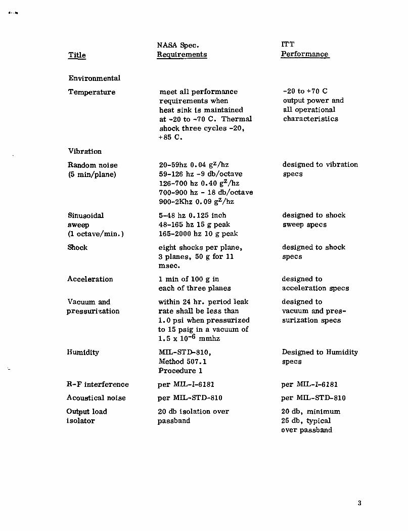
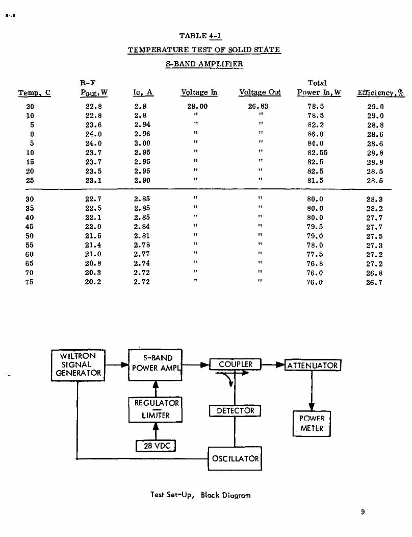
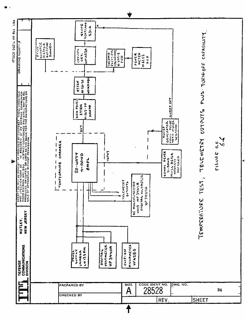
6. TEST PROGRAM 136.1 List of Test Required and Specification Limits 136.2 Description of Tests 136.3 Test Data Sheet 166.4 List of Test Equipment Required 18
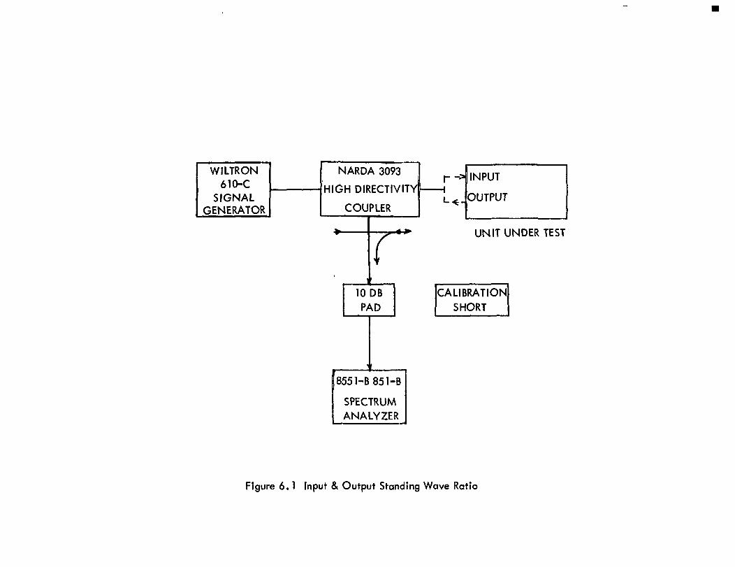
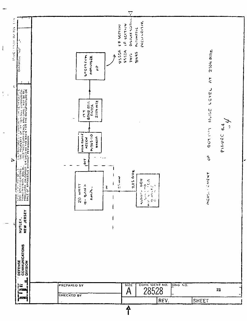
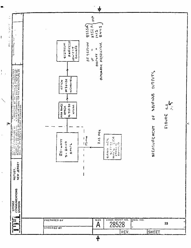
Block Diagrams of measurement set-ups 19 through 24
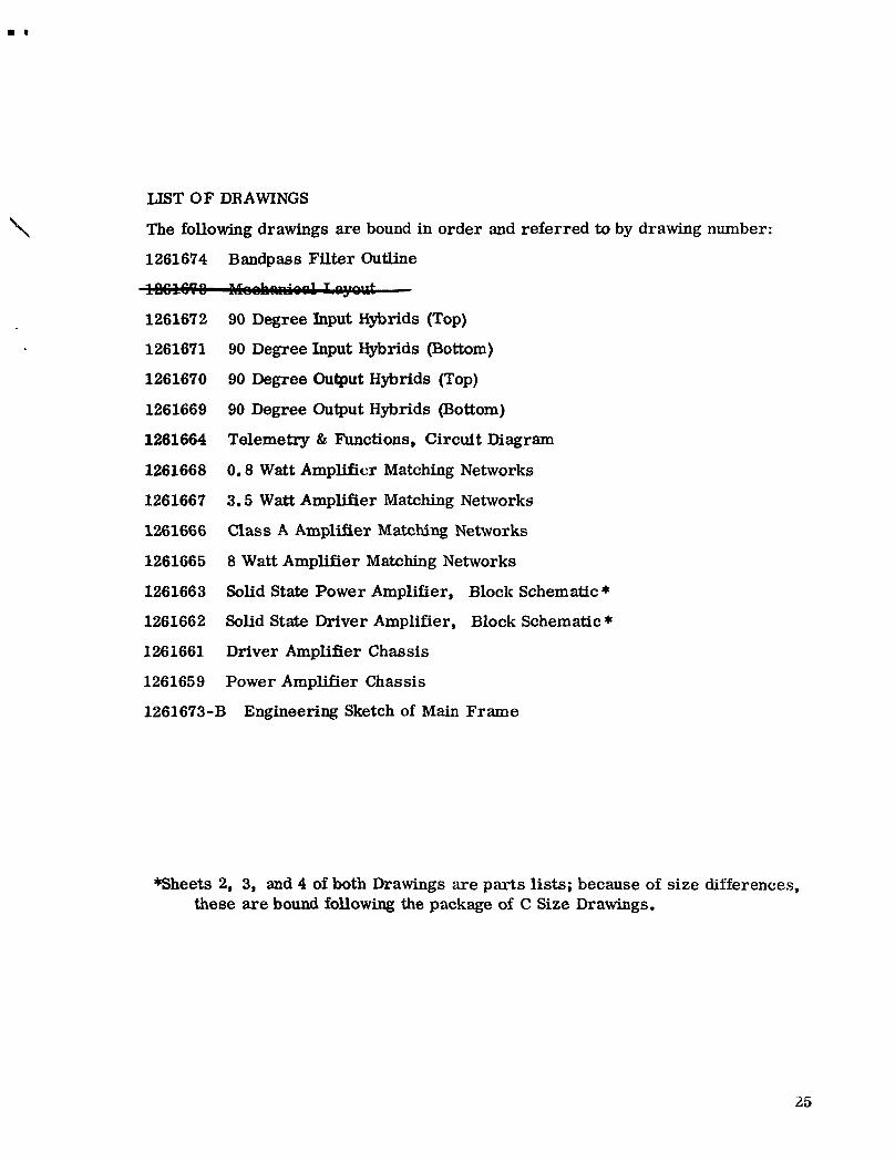
LIST OF DRAWINGS (The drawings listed follow this page) 25
IV
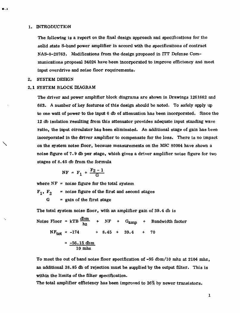
1. INTRODUCTION
The following is a report on the final design approach and specifications for the
solid state S-band power amplifier in accord with the specifications of contract
NAS-8-28763. Modifications from the design proposed in ITT Defense Com-
munications proposal 34024 have been incorporated to improve efficiency and meet
input overdrive and noise floor requirements.
2. SYSTEM DESIGN
2.1 SYSTEM BLOCK DIAGRAM
The driver and power amplifier block diagrams are shown in Drawings 1261662 and
663. A number of key features of this design should be noted. To safely apply up
to one watt of power to the input 6 db of attenuation has been incorporated. Since the
12 db isolation resulting from this attenuator provides adequate input standing wave
ratio, the input circulator has been eliminated. An additional stage of gain has been
incorporated in the driver amplifier to compensate for the loss. There is no impact
on the system noise floor, because measurements on the MSC 80064 have shown a
noise figure of 7.9 db per stage, which gives a driver amplifier noise figure for two
stages of 8.45 db from the formula
FO _ 1NF = F, + ^_-1 G
where NF = noise figure for the total system
Fj, F2 = noise figure of the first and second stages
G = gain of the first stage
The total system noise floor, with an amplifier gain of 39.4 db is
/"^"S'sft?/', fivt'5 ' / o M»« . t s y»ttSHroi.wcO. 2.Z ••,»*.*-:•/*
p£*t\'>Ti>#. ftx£0, 2~i GH*ii, t f9/*
Tft'XVj^viToV, KfpK/ , SM-if^M, <v\St
-rAAN<^TOP.MPM,S«w»ro»/, fc^C
-r<?AM^VTc,^WCW. SlLif^, V.^C
REV
LTRSHT
V4H|
«T/
AT a
AT3
/?/
i
A??
^V
t?S
AT6
0«
02
Q3
U OF M | 1 PIECE 6 PAIR 32 FEET 52 U.S. FLUID OZ. 5J U.S. GAL.A* IN PART NO. COL. DENOTES VENDOR ITEM. SEE— -• •• - ~ "•* cc . D A W ™ I <;rmRrF np SPECIFICATION rnNTROi nwa
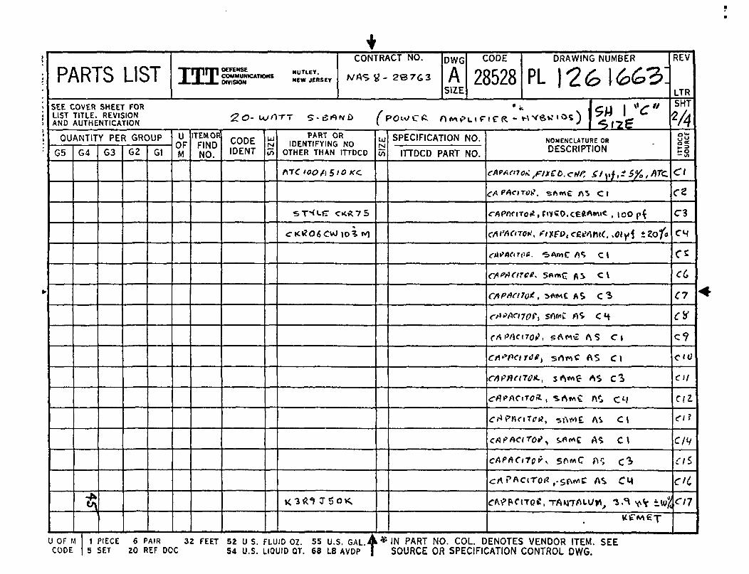
PARTS LIST TITim DEFENSE NUTLEVI ' 1 " I ' COMMUMICATIOMS ZMI «B««JL-L-L. DIVISION "EW JERSEY
SEE COVER SHEET FORLIST TITLE. REVISION 20-WiMT <£> p.ftNOAND AUTHENTICATION
QUANTITY PER GROUP
G5 G4
£
G3 G2 G1
UOFM
ITEM ORFINDNO.
CODEIDENT
UJMI/)
CONTRACT NO.
NP>'» 8-28763
f lnnpi. (DCPA9T OR
IDENTIFYING NO.OTHER THAN ITTDCD
f\-TC 'OVA 510 KC
St>rie CK*7S
c*«OCcw,03^
K 3 1^ *? T -S O K
S.fti-e' FX-HZ.
UlM
DWG
ASIZE
iVCV
CODE
28528
^mPuv \
SPECIFICATION NO.
ITTDCD PART NO.
DRAWING NUMBER
PI 1 C^ ^ 1 f C~U ~
r.CA)
NOMENCLATURE ORDESCRIPTION
CAfAftT'Jti fl/i», Si f>$, t S/4 ftTC
Wmct. rerwwei;.c^M.c. »oo^
cAPfioToft- SAwc A^ C^.
<T^fA<^cP, f txfcC>. CGt?rtfiiC ,0lti4 i 2o/j
CA^^'Toi', Srt"**C fl^ C |
rrtt'lf'To^* ^rtAic rt ^, C2L
rn>v.r.Tt.H.5rt«ie AS c^
fflPAenrt. srtwvT AS Cl
Cflt'rfC t~df?, Sft^cT fl^> Cf
fftffid 1Gk , ^ftcrt£ /^S> Ci
rAPflcir^ii. sf»MC AS CH
^^or«;V, -^vr/U^M, 3.?,,^ i I0/0
VCC^CTT
e»t>*<rrOt. ^ftme «* Cl
FILTER, L\we
REV
LTRSHT
ITTD
CD
SOUR
CE
Cl
cz
C3
C^
cs
CC
C7
C8
C9
CIO
C M
c<z
C/3
fu\
U OF M 1 PIECES SFT
6 PAIR 32 FEET 52 US. FLUID OZ. 55 U.S. GAL.A* IN PART N0. COL. DENOTES VENDOR ITEM: SEEnnr ^/i u <; i mmn or «R i R AWIIP I
PARTS LIST • 1 • DIVISION NEW JERSEY
CONTRACT NO.
U&S S- 28763
DWG
ASIZE
CODE
28528SEE COVER SHEET FORLIST TITLE. REVISION 2O~ WATT 'S-Br^O ftWr>L /PXZvvfi ' Aiv,AND AUTHENTICATION { w m v t K MI^
QUANTITY PER GROUP
G5 G4
^u or M
CODE
G3 G2 G1
UOFM
TEMORFINDNO.
CODEIDENT
LUM
Cfi
PART ORIDENTIFYING NO
OTHER THAN ITTDCD
LUM
c
SPECIFICATION NO.
ITTDCD PART NO.
•
I26I&62*
DRAWING NUMBER
Dl 1 O/" 1 / /* *2 ~iL | cQ? \fok>£
?L* r»c P.)
NOMENCLATURE OR
DESCRIPTION
MATC.V-V6 Neruairic. «,c*i*rrfii»
*AW7CW IV<? k ' '
-*-rrM,v6 ••
MATCf'(A>/> '' '
WftTfUlti/f? '' '
Mfl7r^<>U<7 '• '
IVlrtTf HI ivfj ''
WAft H» V<!, «• ••
tf[f,Te i-'tf^fj ' i'
<=>C\\€\A&\C
REV
LTRSHT
4/4
ITT
DC
DS
OU
RC
E
Zl
-ZZ
Zi
Z*
•zsZd
27
ZS
z?
1 PIECE 6 PAIR 32 FEET 52 U.S. FLUID OZ. 55 U.S. GAL. A* IN PART NO. COL. DENOTES VENDOR ITEM: SEE5 SET 20 REF DOC 54 U S. LIQUID QT. 68 LB AVDP | SOURCE OR SPECIFICATION CONTROL DWG.
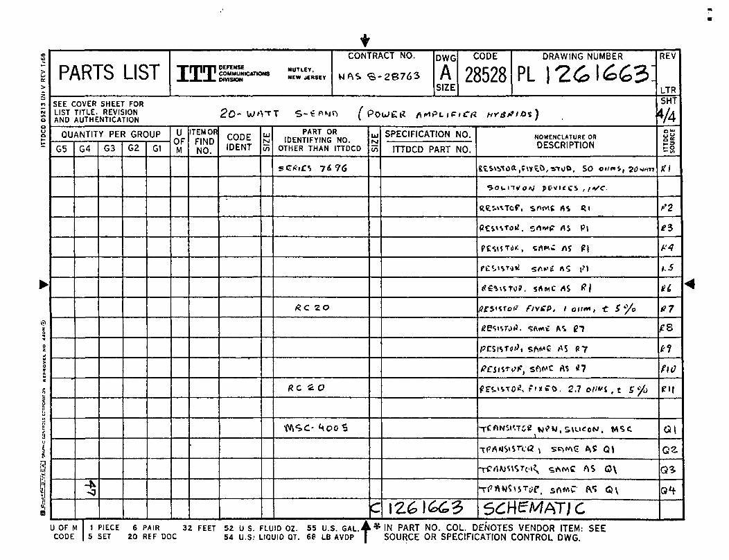
PARTS LIST TTpnP S5KMKM El"'"J-JL.J- DIVISION Me* J£"SEY
CONTRACT NO.
fv/flS tf - 2&7C.3
DWG
ASIZE
SEE COVER SHEET FOR
k!?J IffTLHEENRTgSSNN 20-USn-TT S-^0 fp0*,C* O^O
QUANTITY PER GROUP
G5 G4
*
U OF MCODE
G3 G2 G1
UOFM
ITEM ORFINDNO.
CODEIDENT
uN(75
PART ORIDENTIFYING NO
OTHER THAN ITTDCD
f\TC tOO f\ 5>O K<i
STKLKT CKR75
cK*o<cvo,oi«)
K3<r»TSo*
LUM10
CODE DRAWING NUMBER
28528 PL 1261663!
\ 5ti 1 Vxnf iCR - HVewiOS ) £*.^g
SPECIFICATION NO.
ITTDCD PART NO.
NOMENCLATURE ORDESCRIPTION
<* w«r«: /,f o. c^/r r / rf , * $/„ , />rc
£fl PAflTOI'. SftW£ /^S C 1
rAPnt ITO^ i fiy<«OiCCi'^*^'^ • ioOp4
CAi'ACrtOtf, flT/iff>t f££f\t\t(, .<?ly*i 1 2O/o
^Wftrflis. ->*^C^ Cl
CflPfiCrtCt^ S«rt»C ^5 C I
CflPAfUOt , i M€ AS CS
ff^i>f\cijfff) s»V"C flS C H
Cfi Pfttnof , sAwt <\ S C|
CfiPflftTd*) SrtwC AS Cl
«!«?«*«., s^e ^s c3
(Tfl^ACiT^fZ. , SAwt A^ CM
^HPnriT^, »ftwE AS Cl
crtpAC(7'oi>> s.^«y*C A^ Cl
cftPACiTpr*. 5f\wC ^"i ^3
cM PACiToi* ,-$f\»/iC AS CM
C^fvCtTOi, TAMTrtUUM, •»* ysV tW?
Kt-MET
REV
LTRSHT
tl— in
Cl
<T2
C3
CM
ccC6
CM
C?
CIO
«/ca
< r » ?
c/v^ / S
c/^
07
1 PIECE 6 PAIR 32 FEET 52 US. FLUID 02. 55 U.S. GAL. A* IN PART NO. COL. DENOTES VENDOR ITEM. SEE5 SET 20 REF DOC 54 U.S. LIQUID QT. 68 LB AVDP | SOURCE OR SPECIFICATION CONTROL DWG.
PARTS LIST 1 f 1 11 V 1 OtFEHSC MUTLCV1 • I » 1 1 COMMUNICATIOMS «i"«B.,¥
_L JLJL. DIVISION NEW JERSEY
SEE COVER SHEET FOR
QUANTITY PER GROUP
G5 G4
*
G3 G2 G1
UOFM
TEMORFINDNO.
CODEIDENT
LUM
CONTRACT NO.
N ft ^ Cf — 9 ^ •* / «9* » O C ?^ / fa •%
.o(Pcwc«M, t
PART ORIDENTIFYING NO.
OTHER THAN ITTDCD
An. P/W J83?^
<v<ue FLM2.
I OV\ O2.'Z.'i'5
UM
DWG
ASIZE
if iC
CODE
28528
tf - HYgfll W
SPECIFICATION NO.
ITTDCD PART NO.
DRAWING NUMBER
Dl 1 O S 1 /^" /'"^Z"rL | C.WD \\£>(&^}.
s^NOMENCLATURE OR
DESCRIPTION
I, SAwWPrt lS J.lO.JdHz
ML,
fltTClt. C»N€
cwrtca. aaf t ,„•, s1(uPc;A,t'
CoorLClZ, 3 Hl<5% *?</*. •ST^o't-'^'F
Cfjy/'t.ulZL > "Jcl^i ?(•", ^Tr i tPt '^C
i"C(^/'tiTii , 3 «X& *?0^ jTjk'|Pt»wC
M^tc^W^ A/t7>*;C'*vi<*>( M'C^(JST(/l O
MrtTOl-r, ^TWo«rf. MK.-^TM'
W^Tcv\ilJ(, '/t^TV SCCTtOM, »AtCtOJTl! VC*
Mftltv<imC> '/M"^ 5fJC"noKi, <AVC(<05T|?Vv'
|SOv_ATO<ix ^,2-2,"5Ctiz. . />DOVKi6TOW
REV
LTRSHT
3/4QUl
"«
to
FLl
F«
Kl
"22.
z.*/
ZS
ZC
Z7
zS
H-(\
U OF M 1 PIECE 6 PAIR 32 FEETCODE 5 SET 20 RET DOC
52 U.S. FLUID 02. 55 U S. GAL.54 U.S 'LIQUID OT. 68 LB AVDP t * IN PART NO. COL. DENOTES VENDOR ITEM: SEE
SOURCE OR SPECIFICATION CONTROL DWG.
PARTS LIST ^W"*W^V^V1 DEFFNfiCI ' 1 " 1 ' COMMUNICATIONS H«.LLE».L.,_
J.J_ JL DIVISION MEW "KS"
SEE COVER SHEET FORLIST TITLE. REVISION 2C-UMTT S-€*MAND AUTHENTICATION
QUANTITY PER GROUP
G5 G4
^
G3 G2 G1
U
OFM
TEMORFINDNO.
CODEIDENT
LJM
IO
CONTRACT NO.
^ ( Pouti? ^^f
PART ORIDENTIFYING NO.
OTHER THAN ITTDCD
5C*i£S 7^76
£C 2O
fiC £ O
MSC^OOS
UJ
<Sl
c
DWG
ASIZE
3L 1 P
CODE
28528
iCfi Hf&*
SPECIFICATION NO.
ITTDCD PART NO.
I2£l££5
DRAWING NUMBER
pi | O X \/^/f>'2*~r L 1 .( Itovp^.
' / x>s)
NOMENCLATURE ORDESCRIPTION
ItSWloa.fweft,*™*, 50../«» f90«m
SOU.I**^ , fVI«CS,/- /C.
des«Tof, S««« MS C,
PCStsfotf. Sflvf rtS Pi
P£'i\5lrO*'- , Cfltt£ /^? P|
resisr^ srt^« *5 1?,
• fC^STC?. S r t M C r t S <?|
/?rS'sro(' fivfP, i on**, -t S ^0
HBWTjA, <»ftyrtk AS (?T
/?£SIST<»''« Sh**C AS P7
&£SiVr0ft Sft^C AS tf?
<?rs.>^TO^ f ' x C G . 2.7 o/wi , t IT^O
-rCANSl'.TC? NfW SVU^OW, MSt\
TCrtrtS^STVC \ S^<*\G <S5 Q)
TCrtW^\STC'»^ SAMC ft$ Q\
T^niis^Ttff, sftwcr M Q\
S^H^MAT/C
REV
LTRSHT
*/4
ITT
DC
OS
OU
RC
E
XI
S2
£3
HA
1.5
U
e?
£8
t'f
?\C
*U
til
oaQ^
at
B
B
U OF M 1 PIECE 6 PAIR 32 FEETCODE 5 SET 20 REF DOC 54 U.S.- LIQUID OT. 6C LB AVDPt52 U S. FLUID OZ. 55 U.S. GAL.A* IN PART NO. COL. DENOTES VENDOR ITEM: SEE