27
© Everspin Technologies, Inc. 2011 Technology, Manufacturing and Markets of Magnetoresistive Random Access Memory (MRAM) Brad Engel, VP- Product Development & Quality

© Everspin Technologies, Inc. 2011
Technology, Manufacturing and Markets of Magnetoresistive Random Access Memory (MRAM)
Brad Engel, VP- Product Development & Quality

© Everspin Technologies, Inc. 2011
Everspin – Electron Spin is Forever
Industry-first and leading MRAM supplier Technology leader in Toggle MRAM and ST-MRAM
Shipped over 2.5M units with over 300 active customers to date
Over 15 years of design and production experience with MRAM
Break through non-volatile memory products and IP 70 Products in 3 Memory Families 600 Active Patents and Applications WW
Asynchronous x8, x16 and Serial SPI 176 Issued / 47 Pending US Patents
Backed by leading VC Investors (Spin-out from Freescale in June, 2008)
Global Footprint Headquarters: Chandler, AZ, USA Sales Offices: USA, Europe, China, Japan
Manufacturing: USA, Singapore, Thailand, China Design Center: Austin, TX, USA
Standalone ProductsEmbedded Technology
© Everspin Technologies, Inc. 2011
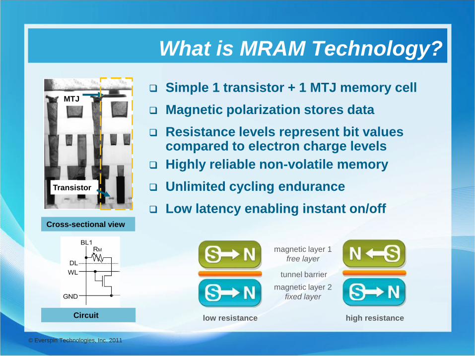
What is MRAM Technology?
Simple 1 transistor + 1 MTJ memory cell
Magnetic polarization stores data
Resistance levels represent bit valuescompared to electron charge levels
Highly reliable non-volatile memory
Unlimited cycling endurance
Low latency enabling instant on/off
magnetic layer 1
free layer
magnetic layer 2
fixed layer
tunnel barrier
high resistancelow resistanceCircuit
Cross-sectional view
MTJ
Transistor

© Everspin Technologies, Inc. 2011
MRAM - Technology Comparison
Toggle Write
Write accomplished by magnetic
fields from current passing through
bit and word lines.
In volume production
Spin-Torque Write
Write accomplished by spin
polarized current passing
through the MTJ.
In development

© Everspin Technologies, Inc. 2011
Everspin MRAM Advantages
Parameter Capability
Non-volatile
capabilityData retention of the bit cell > 20 years
Performance Symmetric read/write – 35ns / 40MHz Serial
Endurance Unlimited cycling endurance
CMOS integration
Easily integrates into back-end process
Compatible with embedded designs No effect on CMOS
Allows for flexible manufacturing
Temperature range
High Temp Storage
-40ºC < T < 150ºC operation demonstrated
Intrinsic reliability > 20 years lifetime at 125ºC
Soft error immunityAlpha radiation soft error rate too low to measure (<0.1 FIT
per Mb) – Everspin partners offer radiation hardened MRAM
Environmentally
friendlyNo battery/caps, RoHS/REACH compliant, instant-on

© Everspin Technologies, Inc. 2011
How is MRAM made?
Shield
Die
Leverage CMOS semiconductor ecosystem Everspin MRAM layer added to standard CMOS
Standard packages with protective internal shield
Common standard package types
Drop in replacement fits footprints for
existing printed circuit board designs
Pin for Pin functionally equivalent
BBSRAM, SPI NVM, nvSRAM and FeRAM

© Everspin Technologies, Inc. 2011
Memory Performance

© Everspin Technologies, Inc. 2011
Memory Performance
ST
-MR
AM

© Everspin Technologies, Inc. 2011
48-BGA
x8 Asynchronous parallel I/O
x16 Asynchronous parallel I/O
x8 Asynchronous parallel 1.8V I/O
Current Toggle MRAM Products
16-bit I/O
Part Number Density Configuration Temp
MR4A16B 16Mb 1M x 16 C,I,A
MR2A16A 4Mb 256K x 16 C,I,E,A
MR0A16A 1Mb 64K x 16 C,I,E,A
8-bit I/O
Part Number Density Configuration Temp
MR4A08B 16Mb 2M x 8 C,I,A
MR2A08A 4Mb 512K x 8 C,I
MR0A08B 1Mb 128K x 8 C,I
MR256A08B 256Kb 32K x 8 C,I
MR0D08B 1Mb 128K x 8, 1.8v I/O C
MR256D08 256Kb 32K x 8, 1.8v I/O C
SPI I/O
Part Number Density Configuration Temp
MR25H40 4Mb 512K x 8 I, A
MR25H10 1Mb 128K x 8 I, A
MR25H256 256Kb 32K x 8 I, A
44-TSOPII, 54-TSOP
x8 Asynchronous parallel I/O
x16 Asynchronous parallel I/O
8-DFN
SPI-compatible serial I/O
40 MHz; No write delay
32-SOIC x8 Asynchronous parallel I/O
Temperatures
Commercial 0 to +70 ºC
Industrial -40 to +85 ºC
Extended -40 to +105 ºC
Automotive -40 to +125 ºC

© Everspin Technologies, Inc. 2011
MRAM Markets & Applications
Industrial Automation & Robotics
Telecom & Datacom Consumer, POS, Gaming
Storage Systems & Servers
Energy ManagementAutomotive & Transportation
Logos, trademarks, images and copyright references are the property of the respective companies noted.

© Everspin Technologies, Inc. 2011
Toggle MRAM Used by Top Companies
“After two years of high volume production and more than 100K systems in the field, we are very happy with the perfect quality and reliability of Everspin’s products in our industrial automation systems” http://www.semiconductor.net/article/CA6658902.html
Everspin Technologies to provide Airbus with MRAM
products for advance wide body aircraft
Flight Control Computer on A350 XQB aircraft uses MRAM for
critical program and data storage in extreme environment
applications.
Everspin Technologies’ MRAM Selected by Emerson Network Power to
Deliver Critical Storage for Industrial Computing Boards
Non-volatile MRAM technology provides a robust, reliable memory solution for VME
and Compact PCI boards.
Siemens Recognizes Everspin Technologies for Perfect MRAM Quality - May, 2009
Automation Technology
11
Everspin's automotive-temperature MRAM meets harsh environment demands in BMW
S1000 RR racing bike
Everspin introduces AEC-Q100 MRAM products to serve broad automotive applications; 4Mb
MRAM stores critical calibration data for BMW Motorsport Super Bike
Logos, trademarks, images and copyright references are the property of the respective companies noted.
© Everspin Technologies, Inc. 2011
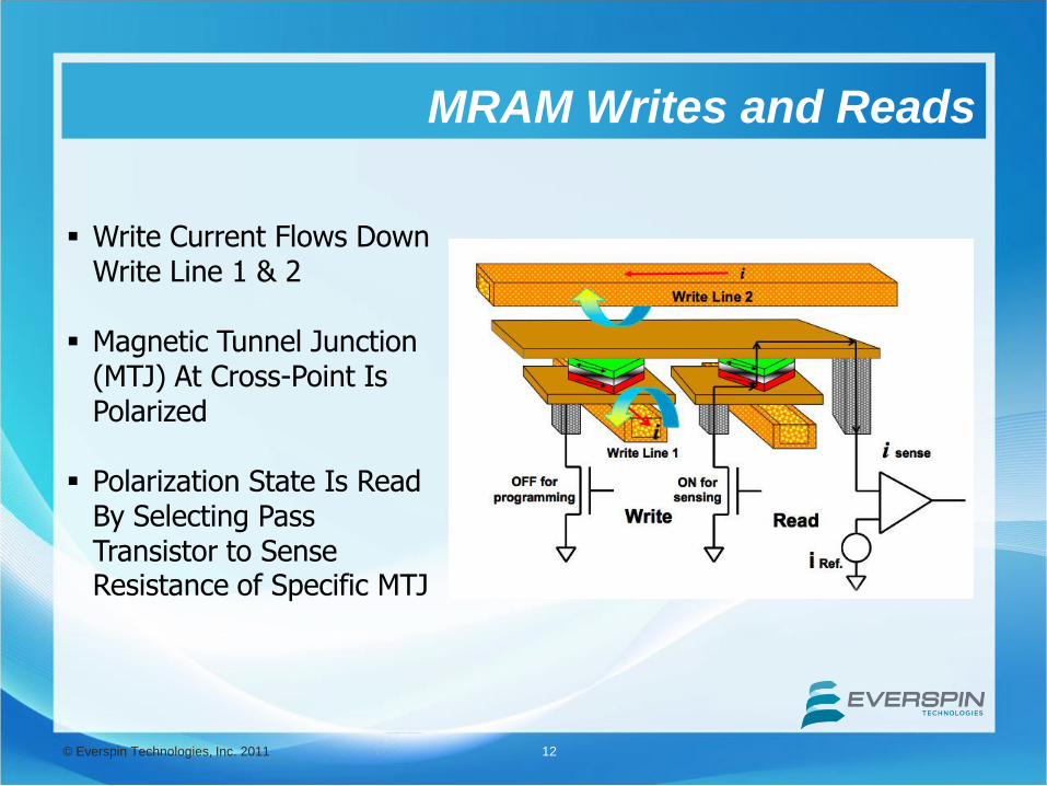
MRAM Writes and Reads
12
Write Current Flows Down Write Line 1 & 2
Magnetic Tunnel Junction (MTJ) At Cross-Point Is Polarized
Polarization State Is Read By Selecting Pass Transistor to Sense Resistance of Specific MTJ

© Everspin Technologies, Inc. 2011 13
MRAM Integration
MRAM
module
Metal 4
Contact
Via 1
Metal 2
Via 2
Metal 4
Via 3
Metal 5
Metal 3
Bit cell
Metal 1
Cu
Cu
Al
Al
Al
MTJ
Metal 4
Metal 5
MTJ

© Everspin Technologies, Inc. 2011 14
Ta
Eg, NiFe, CoFe,
CoFeB
Eg, NiFe, CoFe,
CoFeB
Eg, PtMn, IrMn
Ta/TaNBase electrode
AlOx
Seed
AF pinning layer
Pinned
Ru
Fixed
Top electrode
Free M1
Ru
Free M2Free Synthetic
Antiferromagnet (SAF)
Pinned Synthetic
Antiferromagnet (SAF)
Tunnel barrier
MTJ Bit Materials

© Everspin Technologies, Inc. 2011
MTJ Vertical Profile
Ultra-thin layers require precision control for
manufacturing
15

© Everspin Technologies, Inc. 2011
Toggle MRAM: Write Mechanism
Toggle MRAM is a unique approach that provides both robust
switching performance and manufacturability
Response of synthetic antiferromagnetic free layer is the key.
16
H=0H=0
Conventional MRAM
Single Layer
H≠0
Toggle MRAM
Synthetic Antiferromagnet
H=0 H≠0
Aligns with applied field Rotates perpendicular
to applied field
pinned pinnedpinned pinned
© Everspin Technologies, Inc. 2011
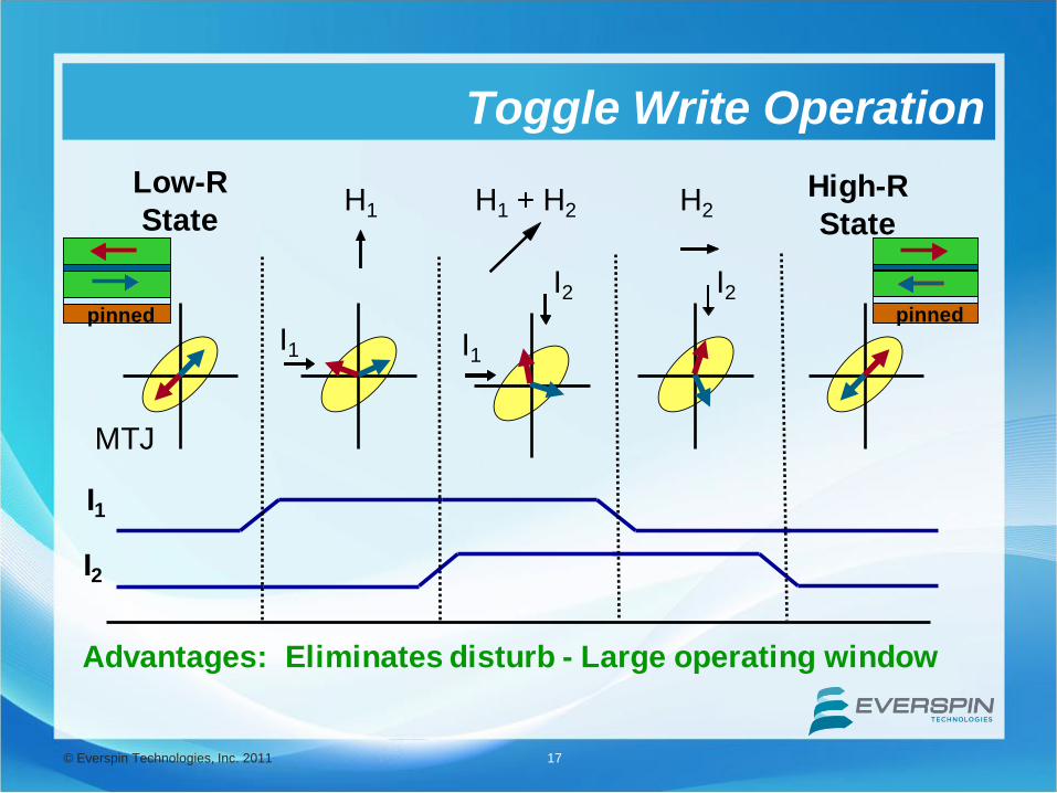
Toggle Write Operation
17
I1
I2
High-R
State
Low-R
StateH1
I1
H1 + H2
I2
H2
Advantages: Eliminates disturb - Large operating window
I2
I1
MTJ
pinned pinned

© Everspin Technologies, Inc. 2011
Robust Toggle-Bit Selection
Robust bit disturb
margin
All bits along ½-selected
current lines have
increased energy barrier
during programming

© Everspin Technologies, Inc. 2011 19
Cu
rren
t I 1
Current I2
No switching
No
sw
itc
hin
g
Switching
Region
Toggle Switching Characteristics

© Everspin Technologies, Inc. 2011
Toggle-bit Array Characteristics
20
H2
toggling
toggling
I
IIIII
IV
No disturb
No disturb
No disturb
No disturb
H2
toggling
toggling
I
IIIII
IV
No disturb
No disturb
No disturb
No disturb
0 7 14 21 28 35 42 49 56 63 70 77 84 91 98 105 112 119 126 133 140
0
9
18
27
36
45
54
63
73
82
91
100
109
118
127
136
145
154
163
172
181
99%-100%
98%-99%
97%-98%
96%-97%
95%-96%
94%-95%
93%-94%
92%-93%
91%-92%
90%-91%
89%-90%
88%-89%
87%-88%
86%-87%
85%-86%i b
it
idigit
Operating
region
0% switching region
(no disturbs)
4Mb, March6N Toggle Map

© Everspin Technologies, Inc. 2011
Write Operating Region at 125 °C
Large write window at Automotive temperatures
21
Operating
Region
T = 125 ºC
Non-Switching
Region
Bit Line Current
Dig
it L
ine
Curr
en
t
Operating
Region
T = 125 ºC
Non-Switching
Region
Bit Line Current
Dig
it L
ine
Curr
en
t
(Oe)
0
50
100
150
200
250
300
0 50 100 150
Temp (°C)
Hsat
Hsw
•Hsat, Hsw decrease linearly w/Temp, reducing window
© Everspin Technologies, Inc. 2011
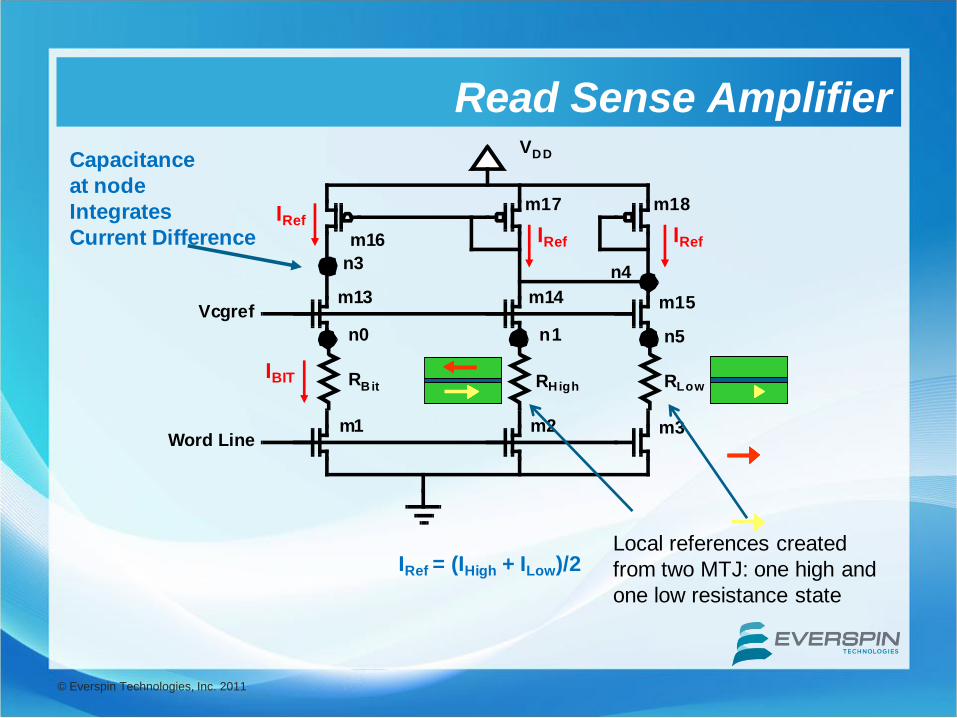
Read Sense Amplifier
Vcgref
RBit
m1 m2 m3
m13 m14 m15
m16
m17 m18
VDD
n5n0 n1
n3n4
Word Line
RLowRHighIBIT
IRef
IRef = (IHigh + ILow)/2
IRefIRef
Capacitance
at node
Integrates
Current Difference
Local references created
from two MTJ: one high and
one low resistance state

© Everspin Technologies, Inc. 2011 23
Magnetoresistance and Distributions
Signal = Rcell – Rref
½ of DR available for sensing
Circuit works at finite bias MR is reduced by bias
dependence of MR
Must sense all bits in the array Circuit must work with bits in tails
of the R distribution
MR = DR/Rlow , DR=Rhigh– RlowArray: Rcell Histogram
Resistance distribution reduces useable MR.
For six-sigma yield in the array, need: DR/2 > 6s

© Everspin Technologies, Inc. 2011
Read Distribution within an Array
24
14 15 16 17 18 190
500
1000
1500
2000
2500
#b
its
Bit Resistance [k]
Low State
High State
s~0.8%
DR/s = 30
typical
10 nm
Optimized for MRAM
Critical Factors:
1. Tunnel barrier quality
2. Pattern fidelity
V1/2~+0.7/-0.55 V

© Everspin Technologies, Inc. 2011 25
MTJ Deposition on 200mm Wafers
Measured uniformity—200 mm
RA=10.4 k-mm2, s=6%
11.3 11.0 10.5 10.5 10.9 12.3
11.7 10.3 9.74 9.88 9.65 9.80 10.2 11.5
10.3 9.54 10.9 10.6 10.3 9.74 10.5
10.1 9.68 10.4 10.8 10.8 10.7 9.85 10.7
9.80 10.9 10.5 10.8 10.5 9.86 10.2
10.3 9.45 10.1 10.4 10.6 9.87 9.62 10.9
10.2 9.52 9.43 9.56 9.59 10.2
11.2 10.2 10.4 11.0
MR=45%, s=2%
43.9 44.5 44.6 44.8 44.5 43.1
44.4 45.0 45.2 46.0 45.8 46.0 44.6 43.1
44.1 45.4 42.9 45.6 45.6 45.8 44.5
44.5 46.1 44.3 45.1 45.5 45.8 46.0 45.0
44.5 45.8 43.4 45.4 45.9 45.7 45.9 44.7
44.2 45.3 45.7 45.5 43.9 45.8 45.4 44.0
44.1 45.3 45.9 45.6 45.0 44.7
43.4 44.0 44.8 44.1
Manufacturable wafer level uniformity and wafer-to-wafer repeatability
• optimization of deposition tool, process, and material stack

© Everspin Technologies, Inc. 2011
Toggle MRAM High Reliability
Predicted lifetime from accelerated testing
Robust reliability at Automotive temperatures
26
1.E+04
1.E+05
1.E+06
1.E+07
1.E+08
1.E+09
1.E+10
1.E+11
1.E+12
55 65 75 85 95 105 115 125
Average Junction Temperature (C)
Lif
eti
me
(h
)
Magnetic Layers
Write Line EM
MTJ R Drift
MTJ TDDB
10 year life20 year life
© Everspin Technologies, Inc. 2011
Summary
MRAM is a highly reliable, high-performance,
nonvolatile memory IC, with unlimited endurance
Has the unique characteristics of a working memory while
providing non-volatility
Current MRAM products are used in a wide variety
of applications
Data Storage, Industrial Control, Medical Systems,
Transportation, Metering and Gaming
Everspin Continues MRAM leadership:
Expanding MRAM into new markets and applications
On track to deliver the industry’s first ST-MRAM
27


