A Multibank Buffer Design with STT-MRAM for High-Bandwidth Low-Power On-Chip Interconnects Hyunjun Jang, Rahul Boyapati, Rohan Kansal, Ki Hwan Yum and Eun Jung Kim Department of Computer Science and Engineering Texas A&M University College Station, Texas, 77843-3112 Email: {hyunjun,rahulboyapati,rkansal,yum,ejkim}@cse.tamu.edu Abstract Network-on-Chip (NoC) is a widely accepted inter-core com- munication infrastructure for Chip Multiprocessors (CMPs). It is critical that NoC provides both low latency and high band- width within limited on-chip power and area budgets. Spin- Transfer Torque Magnetic RAM (STT-MRAM), a high density and low leakage memory, offers more buffer capacities with the same die footprint, thus helping increase network throughput in NoC routers. However, its long latency and power overhead associated with write operations still need to be addressed. In this paper, we propose the first NoC router design that uses only STT-MRAM, which provides much larger buffer space with less power consumption. To hide the multicycle writes, we em- ploy a multibank STT-MRAM buffer, a virtual channel with mul- tiple banks where every incoming flit is seamlessly pipelined to each bank alternately. Our STT-MRAM design has aggres- sively reduced the retention time, resulting in a significant re- duction of the latency and power overheads of write operations. To overcome flit losses caused by the reduced retention time, we propose cost-efficient dynamic buffer refresh schemes that minimize unnecessary refreshes with minimum hardware over- heads. Simulation results show that the proposed STT-MRAM NoC router improves throughput by 21.6% and achieves 17% savings in the total router power compared with a conventional SRAM based NoC router. 1. Introduction Switch-based Network-on-Chip (NoC) has become a popular architecture orchestrating chip-wide communication in Chip Multiprocessors (CMPs). NoC should be carefully designed due to its inherent constraints of the restricted power and area budgets in a chip. NoC consumes up to 28% of the chip power [25], and among the different components comprising on-chip interconnects, buffers are the largest leakage power consumers in NoC routers, consuming about 68% of the total router leakage power [12]. Buffers also consume significant dy- namic power [51, 56], and this consumption increases rapidly as data flow rates increase [56]. Consequently, designing an innovative buffer structure plays a crucial role in architecting high performance and low power on-chip interconnects. Spin-Transfer Torque Magnetic RAM (STT-MRAM) [38, 44, 48, 57] is a promising next generation memory technol- ogy that can replace conventional RAMs due to its near-zero leakage power and high density. Adopting STT-MRAM in NoC has significant merits since an on-chip router can pro- vide larger input buffers under the same area budget compared with conventional SRAM routers. Larger input buffers con- tribute to improving throughput, which results in enhanced sys- tem performance with less power consumption. STT-MRAM is CMOS-compatible, and provides virtually infinite write en- durance [20] compared with other memory technologies such as Phase Change Memory (PCM) [28], Flash, and Memris- tor [24], which makes STT-MRAM a more viable solution as an on-chip memory that should tolerate frequent write accesses. Besides, STT-MRAM is immune to the radiation induced soft errors [46, 47], thus providing robust cell storages, and can scale beyond 10 nm technology [15]. However, the weaknesses of STT-MRAM, long latency and high power consumption in write operations, should be properly addressed because fast ac- cesses to on-chip memories must be assured for high perfor- mance NoCs. Several studies have been performed to address these write speed and energy limitations of STT-MRAM in designing caches and NoC routers. An adaptive block placement and migration policy for hybrid STT-RAM and SRAM last level caches has been proposed in [52]. An SRAM/MRAM hybrid cache with 3D stacking structure was proposed in [45]. A region-based hybrid cache [54] with small fast SRAM and large slow MRAM mitigates performance degradation and energy overheads. For NoC routers, an SRAM/STT-MRAM hybrid buffer [27] shows substantial throughput improvements across various workloads. However, the inevitable use of SRAM to hide the multicycle writes of STT-MRAM sacrifices area, and wastes significant dynamic power in migrating data between the disparate memories. The leakage power overhead due to SRAM also increases as network scale grows and technology scales down [5]. In this paper, we propose the first NoC router design that uses only STT-MRAM in buffers. By eliminating SRAM, it offers much larger buffer space with less power consumptions. To hide the multicycle write latencies of STT-MRAM, we pro- pose a novel pipelined input buffer design, a multibank STT- MRAM buffer, which is a virtual channel (VC) with multiple banks where every incoming flit is delivered to each bank alter- nately via a simple latch inside a router. Through this, we can avoid performance degradation while consuming less area and power. For our design, we use the write latency reduction tech- nique [48], which sacrifices the data retention time of an Mag- netic Tunnel Junction (MTJ), a bit storage of STT-MRAM. This can be possible due to the short intra-router latency 1 of a flit in on-chip routers as shown in Figure 1, where the average intra- router latency is less than 3 cycles 2 . However, for applications that exhibit bursty communication and have heavy loads, we ob- serve that flits are staying in STT-MRAM buffers longer than 1 An intra-router latency is the time interval between the arrival of a flit at an input buffer and the departure from a router through a crossbar. 2 See Section 5 for detailed system configuration.
Transcript
A Multibank Buffer Design with STT-MRAMfor High-Bandwidth Low-Power On-Chip Interconnects
Hyunjun Jang, Rahul Boyapati, Rohan Kansal, Ki Hwan Yum and Eun Jung KimDepartment of Computer Science and Engineering
AbstractNetwork-on-Chip (NoC) is a widely accepted inter-core com-
munication infrastructure for Chip Multiprocessors (CMPs). Itis critical that NoC provides both low latency and high band-width within limited on-chip power and area budgets. Spin-Transfer Torque Magnetic RAM (STT-MRAM), a high densityand low leakage memory, offers more buffer capacities with thesame die footprint, thus helping increase network throughputin NoC routers. However, its long latency and power overheadassociated with write operations still need to be addressed. Inthis paper, we propose the first NoC router design that usesonly STT-MRAM, which provides much larger buffer space withless power consumption. To hide the multicycle writes, we em-ploy a multibank STT-MRAM buffer, a virtual channel with mul-tiple banks where every incoming flit is seamlessly pipelinedto each bank alternately. Our STT-MRAM design has aggres-sively reduced the retention time, resulting in a significant re-duction of the latency and power overheads of write operations.To overcome flit losses caused by the reduced retention time,we propose cost-efficient dynamic buffer refresh schemes thatminimize unnecessary refreshes with minimum hardware over-heads. Simulation results show that the proposed STT-MRAMNoC router improves throughput by 21.6% and achieves 17%savings in the total router power compared with a conventionalSRAM based NoC router.
1. Introduction
Switch-based Network-on-Chip (NoC) has become a populararchitecture orchestrating chip-wide communication in ChipMultiprocessors (CMPs). NoC should be carefully designeddue to its inherent constraints of the restricted power and areabudgets in a chip. NoC consumes up to 28% of the chippower [25], and among the different components comprisingon-chip interconnects, buffers are the largest leakage powerconsumers in NoC routers, consuming about 68% of the totalrouter leakage power [12]. Buffers also consume significant dy-namic power [51, 56], and this consumption increases rapidlyas data flow rates increase [56]. Consequently, designing aninnovative buffer structure plays a crucial role in architectinghigh performance and low power on-chip interconnects.
Spin-Transfer Torque Magnetic RAM (STT-MRAM) [38,44, 48, 57] is a promising next generation memory technol-ogy that can replace conventional RAMs due to its near-zeroleakage power and high density. Adopting STT-MRAM inNoC has significant merits since an on-chip router can pro-vide larger input buffers under the same area budget comparedwith conventional SRAM routers. Larger input buffers con-tribute to improving throughput, which results in enhancedsys-tem performance with less power consumption. STT-MRAM
is CMOS-compatible, and provides virtually infinite write en-durance [20] compared with other memory technologies suchas Phase Change Memory (PCM) [28], Flash, and Memris-tor [24], which makes STT-MRAM a more viable solution asan on-chip memory that should tolerate frequent write accesses.Besides, STT-MRAM is immune to the radiation induced softerrors [46, 47], thus providing robust cell storages, and canscale beyond 10nmtechnology [15]. However, the weaknessesof STT-MRAM, long latency and high power consumption inwrite operations, should be properly addressed because fast ac-cesses to on-chip memories must be assured for high perfor-mance NoCs.
Several studies have been performed to address these writespeed and energy limitations of STT-MRAM in designingcaches and NoC routers. An adaptive block placement andmigration policy for hybrid STT-RAM and SRAM last levelcaches has been proposed in [52]. An SRAM/MRAM hybridcache with 3D stacking structure was proposed in [45]. Aregion-based hybrid cache [54] with small fast SRAM and largeslow MRAM mitigates performance degradation and energyoverheads. For NoC routers, an SRAM/STT-MRAM hybridbuffer [27] shows substantial throughput improvements acrossvarious workloads. However, the inevitable use of SRAM tohide the multicycle writes of STT-MRAM sacrifices area, andwastes significant dynamic power in migrating data betweenthe disparate memories. The leakage power overhead due toSRAM also increases as network scale grows and technologyscales down [5].
In this paper, we propose the first NoC router design thatuses only STT-MRAM in buffers. By eliminating SRAM, itoffers much larger buffer space with less power consumptions.To hide the multicycle write latencies of STT-MRAM, we pro-pose a novel pipelined input buffer design, a multibank STT-MRAM buffer, which is a virtual channel (VC) with multiplebanks where every incoming flit is delivered to each bank alter-nately via a simple latch inside a router. Through this, we canavoid performance degradation while consuming less area andpower.
For our design, we use the write latency reduction tech-nique [48], which sacrifices thedata retention timeof an Mag-netic Tunnel Junction (MTJ), a bit storage of STT-MRAM. Thiscan be possible due to the short intra-router latency1 of a flit inon-chip routers as shown in Figure1, where the average intra-router latency is less than 3 cycles2. However, for applicationsthat exhibit bursty communication and have heavy loads, we ob-serve that flits are staying in STT-MRAM buffers longer than
1An intra-router latency is the time interval between the arrival of a flit atan input buffer and the departure from a router through a crossbar.
2 See Section5 for detailed system configuration.
0
1
2
3
4
5
Avg
In
tra
-Ro
ute
r La
ten
cy
(Cyc
les)
Figure 1: Average Intra-Router Latencies in PARSEC Bench-marks in an (8x8) Mesh Network
55
97
88
28
47
33
15
39
35
87
04
9
67
39
7
38
48
0
13
99
5
10
18
7
84
47
50
32
30
72
24
62
19
85
19
46
39
21
0
100000
200000
300000
400000
500000
600000
700000
800000
900000
1000000
0.0
0.5
1.0
1.5
2.0
2.5
3.0
< 1
0
20
40
60
80
10
0
12
0
14
0
16
0
18
0
20
0
22
0
24
0
26
0
28
0
30
0
> 3
20
Nu
mb
er o
f Flits %
of
Tota
l F
lits
Intra-router Latency (Cycles)
% of Total Flits Number of Flits(98.5)
Figure 2: Per-Application Intra-Router Latency Distribut ion(canneal in PARSEC Benchmarks)
a given retention time, which results in flit losses3. This isbecause some flits have fairly high intra-router latencies whilemost of the flits are clustered around low intra-router latenciesless than 10 cycles as shown in Figure2. These lost flits in-cur noticeable performance losses especially when the flitsareparts of control packets carrying critical cache coherenceinfor-mation. On average, 78.7% of traffic is such single-flit controlpackets in PARSEC benchmarks [36]. Therefore, we proposecost-efficient dynamic buffer refresh schemes, the processes inwhich cells’ values are kept valid by triggering refreshes in atimely manner with minimum hardware overheads.
The main contributions of this paper are as follows:• We present a detailed analysis on design tradeoffs of an MTJ
especially in terms of write performance, write power, and re-tention time, which are suitable for performance- and power-efficient NoCs.
• We propose a novel multibank input buffer design, which isimplemented entirely with STT-MRAM and delivers optimalpower saving and performance improvement.
• We suggest cost-efficient dynamic buffer refresh schemes: asimple refresh scheme and a global counter refresh scheme,which selectively trigger buffer refreshments in a power effi-cient manner to maintain the validity of flits.
• We achieve 21.6% throughput improvement and 17% to-tal power saving compared to a conventional SRAM basedrouter with the proposed STT-MRAM router scheme.
2. Background
In this section, we review key features of STT-MRAM and ana-lyze design tradeoffs of an MTJ cell in terms of switching time(the time taken for completing a write operation in an MTJ cell,namely write latency), switching current (the power requiredto change an MTJ cell value, namely write power), and dataretention time.
2.1. STT-MRAM
STT-MRAM is a next generation memory technology that ex-ploits magnetoresistance for storing data [38, 44, 48, 57]. InSTT-MRAM, each data bit is stored in an MTJ, a fundamentalbuilding block. An MTJ consists of three layers: two ferro-magnetic layers and a Magnesium Oxide (MgO) tunnel barrierlayer in the middle as shown in Figure3. The magnetization di-rection of the bottom ferromagnetic layer is fixed. The spin of
3 The increased buffer capacity potentially exacerbates theflit losses prob-lem because the average turnaround time for the router to serve each flit isincreased accordingly. This problem can be alleviated by adopting a bandwidth-efficient routing algorithm [36], or by fine-tuning the retention time [48].
Free Layer
Tunnel Barrier (MgO)
Fixed Layer
Bit Line
Source Line
MTJ
NMOS
Transistor
Wo
rd L
ine
Tunnel Barrier (MgO)
Tunnel Barrier (MgO)
(a) Parallel (0)
(b) Anti-Parallel (1)
Figure 3: STT-MRAM Cell Structure
the electrons in the top layer is influenced by a high-amplitudecurrent pulse that propagates through the fixed layer. Depend-ing on the current, the spin polarity of the free layer changesto either parallel or anti-parallel to that of the fixed layer. Theparallel indicates a zero state and the anti-parallel a one state asshown in Figure3. A single MTJ module is coupled with anNMOS transistor to form a basic memory cell of STT-MRAM,called a 1T-1MTJ.
2.2. STT-MRAM Design Considerations
• Retention Time: The nonvolatility of an MTJ is quantita-tively measured by thedata retention time, which is the max-imum time duration for which stored data can remain in anMTJ [29, 44]. The data retention time, Tret, of an MTJ is de-fined as follows [42].
Tret = 1ns·e∆
∆ is the thermal factorthat estimates thermal stability of anMTJ, and it is proportional to the saturation magnetization(Ms),the in-plane anisotropy field (Hk), and the volume of an MTJcell (V) as follows [11]. T denotes the working temperature.
∆ ∝MsHkV
T
We decrease thethermal factorby reducingMs andHk, leadingto reduced retention-time STT-MRAM [44]. Note that the de-creased thermal stability might hurt the soft error robustness ofSTT-MRAM, thus potentially incurring random bit-flips [43],but this problem can be solved by adopting suitable soft errorprotection schemes for STT-MRAM [47, 49].• Switching Current and Switching Time: In a precessionalswitching mode[41] where an MTJ switching time (Ts) is short(< 3 ns), the requiredcurrent density, Jc(Ts), is determined asfollows.
Jc(Ts) ∝ Jc0+CTs ,
2
0
50
100
150
200
250
300
0.0 0.5 1.0 1.5 2.0 2.5 3.0
Sw
itch
ing
Cu
rre
nt
(uA
)
Switching Time (ns)
10 years 1 sec 10 ms 100 ns
Write Performance Overhead
Wri
te P
ow
er
Ov
erh
ea
d
Retention Time :
Figure 4: The Relationship between Switching Current andSwitching Time for Different MTJ Retention Times
whereJc0 is a switching threshold current density that also de-pends onMs andHk [57] like the thermal factor(∆). C is aconstant affected by the initial angle between the magnetiza-tion vector of the free layer and the easy axis [48]. Reducingthe retention time causes thethermal factorto decrease, whichreducesMs and Hk, and eventually decreasesJc0. Therefore,with smallerJc0, we can achieve a shorter switching time withthe reducedcurrent density, Jc(Ts).
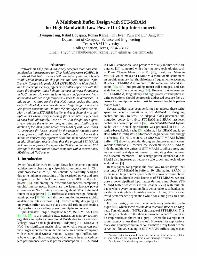
Figure4 depicts the inverse relationship between the switch-ing current (Jc(Ts)) and the switching time (Ts) under four dif-ferent MTJ retention times ranging from 10 years to 100ns.The retention time curves in Figure4 are plotted based on previ-ous studies [29, 44, 48], where the retention time is reduced upto tens ofµs level, and for our STT-MRAM buffer design, wefurther reduce the retention time to 100ns (proven to be feasi-ble in [10]) based on MTJ device equations [29] and simulationwith the PTM model [4] under 32nmtechnology. As we furtherreduce the retention time, the required MTJ switching time andswitching current get decreased accordingly, leading to betterwrite performance and less write power overhead. When fixingthe switching time at 1.0ns, for instance, we can reduce thewrite current by 45.2% by relaxing the retention time from 10ms to 100ns. Based on this analysis, we integrate the buffer-level SRAM and STT-MRAM models in NVsim [14] and sim-ulation results are shown in Table2.
• Cell Area: As an area model of STT-MRAM, we refer toITRS projections [26] as well as the model used in [20], wherea 1T-1MTJ size is 30F2. When we assume that an SRAMcell size is approximately 146F2 under 32nmtechnology, oneSRAM cell can be substituted by at least four STT-MRAM cellsunder the same area budget. An STT-MRAM cell area is mostlydetermined by the NMOS transistor size since the MTJ cell ismuch smaller than the transistor [20].
• Impact of Process Technology:Applying different pro-cess technologies can affect the overall STT-MRAM power-performance cost. As process technologies scale down, the fu-ture STT-MRAM is predicted to achieve a significantly smallercell size, faster read/write with lower power consumption whilemaintaining the non-volatility property [15, 49]. For advancedtechnologies such as 22nm, NVsim [14] circuit-level simu-lation shows that the cell area is decreased by 48.4%, theread/write dynamic power by 13%, and the leakage power by41.4% compared to those of 32nm. The write delay can also bedecreased further due to the smaller cell size and less current re-quired for bit-flips. These trends indicate that STT-MRAM willbecome a more viable option for cost-efficient NoC routers.
0
10
20
30
40
50
60
70
80
90
100
0 0.05 0.1 0.15 0.2 0.25 0.3 0.35 0.4 0.45
Late
ncy
(C
ycle
s)
Injection Rate (flits/node/cycle)
SRAM4 STT16 (baseline) STT16 (no-lat)
Figure 5: Performance Comparison between SRAM and STT-MRAM based Routers under the Same Area Budget
3. Motivation
In this section, we present key motivations that drive us toSTT-MRAM based NoC routers for power and performance co-optimization.
3.1. STT-MRAM for NoC Routers
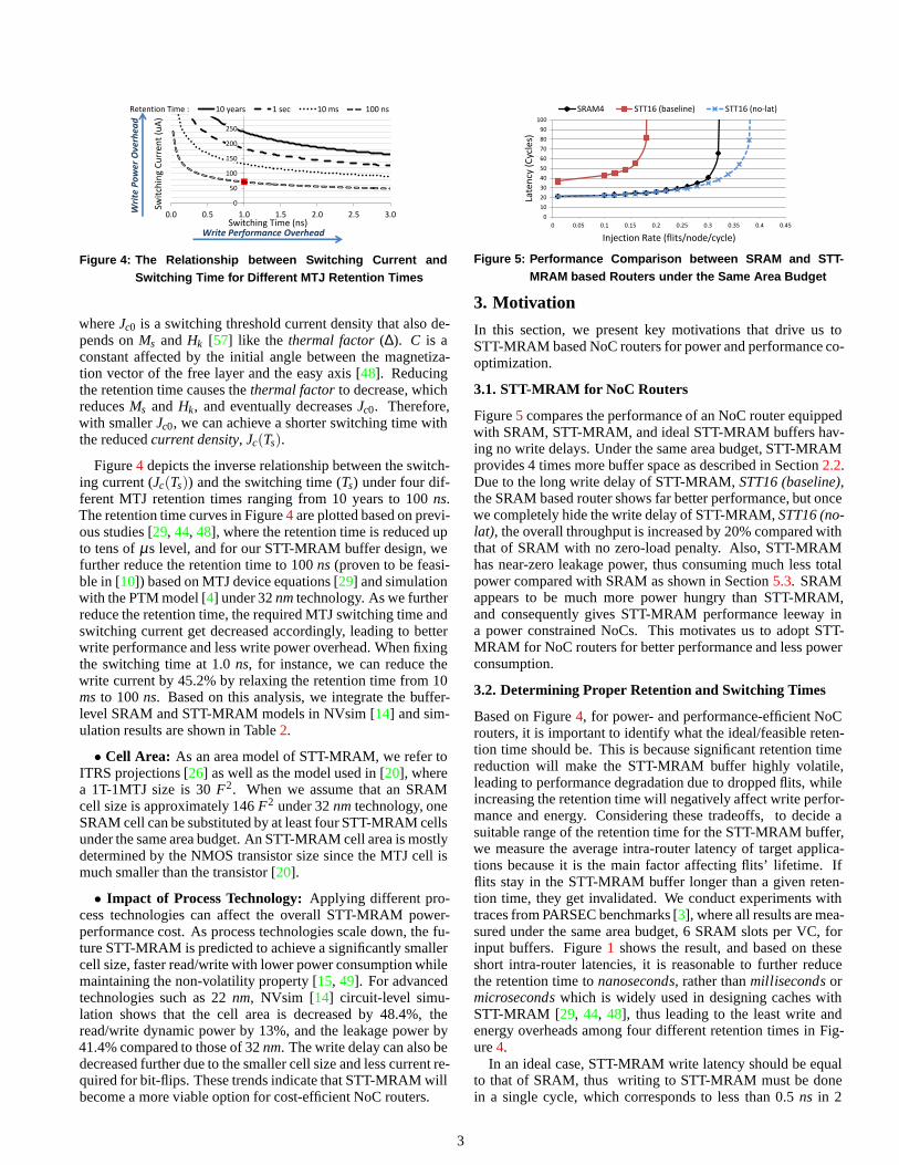
Figure5 compares the performance of an NoC router equippedwith SRAM, STT-MRAM, and ideal STT-MRAM buffers hav-ing no write delays. Under the same area budget, STT-MRAMprovides 4 times more buffer space as described in Section2.2.Due to the long write delay of STT-MRAM,STT16 (baseline),the SRAM based router shows far better performance, but oncewe completely hide the write delay of STT-MRAM,STT16 (no-lat), the overall throughput is increased by 20% compared withthat of SRAM with no zero-load penalty. Also, STT-MRAMhas near-zero leakage power, thus consuming much less totalpower compared with SRAM as shown in Section5.3. SRAMappears to be much more power hungry than STT-MRAM,and consequently gives STT-MRAM performance leeway ina power constrained NoCs. This motivates us to adopt STT-MRAM for NoC routers for better performance and less powerconsumption.
3.2. Determining Proper Retention and Switching Times
Based on Figure4, for power- and performance-efficient NoCrouters, it is important to identify what the ideal/feasible reten-tion time should be. This is because significant retention timereduction will make the STT-MRAM buffer highly volatile,leading to performance degradation due to dropped flits, whileincreasing the retention time will negatively affect writeperfor-mance and energy. Considering these tradeoffs, to decide asuitable range of the retention time for the STT-MRAM buffer,we measure the average intra-router latency of target applica-tions because it is the main factor affecting flits’ lifetime. Ifflits stay in the STT-MRAM buffer longer than a given reten-tion time, they get invalidated. We conduct experiments withtraces from PARSEC benchmarks [3], where all results are mea-sured under the same area budget, 6 SRAM slots per VC, forinput buffers. Figure1 shows the result, and based on theseshort intra-router latencies, it is reasonable to further reducethe retention time tonanoseconds, rather thanmillisecondsormicrosecondswhich is widely used in designing caches withSTT-MRAM [29, 44, 48], thus leading to the least write andenergy overheads among four different retention times in Fig-ure4.
In an ideal case, STT-MRAM write latency should be equalto that of SRAM, thus writing to STT-MRAM must be donein a single cycle, which corresponds to less than 0.5ns in 2
3
0
250
500
750
1000
1250
1500
1750
2000
Nu
m o
f F
lits
Dro
pp
ed
(8359) (2353) (3436)
(a) Different Applications (PARSEC, ret: 100 ns)
0
2000
4000
6000
8000
10000
12000
14000
0 0.1 0.2 0.3 0.4 0.5 0.6 0.7
Nu
mb
er
of
flit
s d
rop
pe
d
Injection Rate (flits/node/cycle)
10ns(20cycles) 50ns(100cycles) 100ns(200cycles)
150ns(300 cycles) 200ns(400cycles)
(b) Different Retention Times (UR)
0
5000
10000
15000
20000
25000
30000
35000
40000
0 0.1 0.2 0.3 0.4 0.5 0.6 0.7Nu
mb
er
of
flit
s d
rop
pe
d
Injection Rate (flits/node/cycle)
(16x16) mesh (12x12) mesh (8x8) mesh
(c) Different Network Scales (UR, ret: 100 ns)
Figure 6: NoC Factors Affecting the Number of Flits Dropped
GHz clock frequency. Such fast write times of less than 0.5nshave proved possible [10, 49], but as shown in Figure4, itrequires rather strong currents, and is far from the optimalef-ficiency [50]. Even with the shortest retention time, therefore,we conclude that it is inevitable to have more than 1-cycle la-tency for a write operation in the STT-MRAM buffer.
Our proposed scheme exploits these observations to accel-erate STT-MRAM write speeds with less power consumption.In Section4.2, we propose router architectures that effectivelyhide the multicycle write latencies of STT-MRAM.
In summary, for power-performance co-optimized STT-MRAM buffer design, as detailed in Section2.2, we reduce theretention time to 100ns, and through this, 2-cycle write latency,corresponding to 1ns in 2 GHz clock frequency, is achievedwith 71.35µA of switching current (See the point where 100ns retention and 1.0ns switching time intersect in Figure4)with 30F2 of STT-MRAM cell size.
3.3. Avoiding Flit Losses
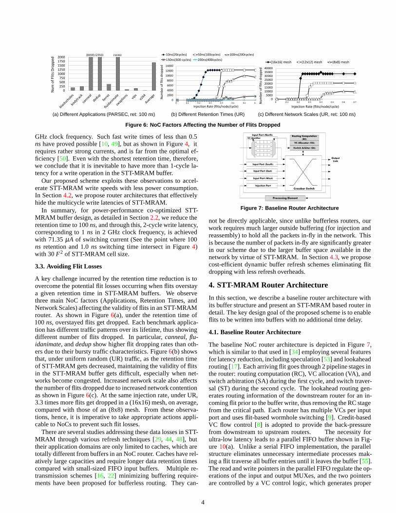
A key challenge incurred by the retention time reduction is toovercome the potential flit losses occurring when flits overstaya given retention time in STT-MRAM buffers. We observethree main NoC factors (Applications, Retention Times, andNetwork Scales) affecting the validity of flits in an STT-MRAMrouter. As shown in Figure6(a), under the retention time of100ns, overstayed flits get dropped. Each benchmark applica-tion has different traffic patterns over its lifetime, thus showingdifferent number of flits dropped. In particular,canneal, flu-idanimate, anddedupshow higher flit dropping rates than oth-ers due to their bursty traffic characteristics. Figure6(b) showsthat, under uniform random (UR) traffic, as the retention timeof STT-MRAM gets decreased, maintaining the validity of flitsin the STT-MRAM buffer gets difficult, especially when net-works become congested. Increased network scale also affectsthe number of flits dropped due to increased network contentionas shown in Figure6(c). At the same injection rate, under UR,3.3 times more flits get dropped in a (16x16) mesh, on average,compared with those of an (8x8) mesh. From these observa-tions, hence, it is imperative to take appropriate actions appli-cable to NoCs to prevent such flit losses.
There are several studies addressing these data losses in STT-MRAM through various refresh techniques [29, 44, 48], buttheir application domains are only limited to caches, whicharetotally different from buffers in an NoC router. Caches haverel-atively large capacities and require longer data retentiontimescompared with small-sized FIFO input buffers. Multiple re-transmission schemes [16, 22] minimizing buffering require-ments have been proposed for bufferless routing. They can-
Routing Computation (RC)
VC Allocator (VA)
Switch Arbiter (SA)
VC Identifier
Input Port (North)
Crossbar Switch
Processing Element
Input Port (West)
Input Port (East)
Input Port (South)
Injection Port
Output Link
Figure 7: Baseline Router Architecture
not be directly applicable, since unlike bufferless routers, ourwork requires much larger outside buffering (for injectionandreassembly) to hold all the packets in-fly in the network. Thisis because the number of packets in-fly are significantly greaterin our scheme due to the larger buffer space available in thenetwork by virtue of STT-MRAM. In Section4.3, we proposecost-efficient dynamic buffer refresh schemes eliminatingflitdropping with less refresh overheads.
4. STT-MRAM Router Architecture
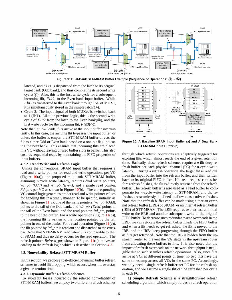
In this section, we describe a baseline router architecturewithits buffer structure and present an STT-MRAM based router indetail. The key design goal of the proposed scheme is to enableflits to be written into buffers with no additional time delay.
4.1. Baseline Router Architecture
The baseline NoC router architecture is depicted in Figure7,which is similar to that used in [34] employing several featuresfor latency reduction, including speculation [53] and lookaheadrouting [17]. Each arriving flit goes through 2 pipeline stages inthe router: routing computation (RC), VC allocation (VA), andswitch arbitration (SA) during the first cycle, and switch traver-sal (ST) during the second cycle. The lookahead routing gen-erates routing information of the downstream router for an in-coming flit prior to the buffer write, thus removing the RC stagefrom the critical path. Each router has multiple VCs per inputport and uses flit-based wormhole switching [9]. Credit-basedVC flow control [8] is adopted to provide the back-pressurefrom downstream to upstream routers. The necessity forultra-low latency leads to a parallel FIFO buffer shown in Fig-ure 10(a). Unlike a serial FIFO implementation, the parallelstructure eliminates unnecessary intermediate processesmak-ing a flit traverse all buffer entries until it leaves the buffer [55].The read and write pointers in the parallel FIFO regulate theop-erations of the input and output MUXes, and the two pointersare controlled by a VC control logic, which generates proper
4
read and write pointer values and status signals.
4.2. STT-MRAM Router Design
For conventional SRAM buffers, incoming flits are written totheir designated buffers with no delay due to the short SRAMwrite latency. On the contrary, when we replace SRAM withSTT-MRAM, only a single flit can be written to a buffer ev-ery n cycles, which causes subsequent incoming flits to be de-layed. To guarantee seamless traversal of flits across the net-work, we propose a multibank STT-MRAM buffer that hidesthe long write latency inherent in STT-MRAM.4.2.1. Multibank STT-MRAM BufferThe multibank buffer scheme can be used to hiden-cycle writelatency of STT-MRAM. For example, to hide 2-cycle write de-lay of STT-MRAM buffer, we divide each VC into two bankswhere every incoming flit is seamlessly pipelined to each bankalternately via a simple latch inside a router. Note that manystudies [12, 13, 31, 18] explore the latch-based NoC pipelinedesign, where latches along the link are utilized as temporarybuffers that can hold and release data when necessary. The sim-ple latch in this paper is controlled by a control block [13] inter-faced with the NoC clock, having the dual function of switchingbetween storing and transmitting data. Let us refer to the twobanks asOdd andEvenbanks, respectively, and incoming flitsfrom upstream routers as Odd and Even flits as shown in Fig-ure8(a). Every odd numbered flit is sent to the Odd bank of adownstream router, and similarly, an even numbered flit to theEven bank through a Multibank Buffer Arbiter (MBA) that hasone input port and two splitted output ports.
The goal of this multibank buffer scheme is to enable theincoming consecutive flits to be written to different banks si-multaneously to effectively hide the multicycle write latenciesof STT-MRAM. To achieve this goal, two MUXes and one sim-ple latch are used for the MBA as shown in Figure8(b). EachMUX has two inputs: one input is connected to the communi-cation link from the upstream router, and another to the simplelatch inside the router. The simple latch is located at the frontof the input buffer and functions as a temporary buffer. It holdsan incoming flit for a cycle and dispatches the latched flit to itsoriginal target bank at the very next cycle.Iclk andMclk arecontrol signals originating from the control block in the inputbuffer, which represent the hold/release signals for the latch.The area overhead for this logic is negligible as compared tothe buffer, and already added to the logic area controlling re-fresh/read/write pointers. An incoming Odd flit, for instance,is directly written to the Odd bank during the first cycle, andthen during the next cycle, the latched flit is sent to the sameOdd bank, thus completing its 2-cycle write process4. Simi-larly, a subsequent incoming Even flit follows the same pro-cess, but uses the other bank. Through this, without the needof any additional SRAM buffer as in the Hybrid buffer [27], wecan seamlessly pipeline incoming consecutive flits to the inputbuffers of a downstream router.
Note that, in case of very light loads, an incoming flit mightexperience write delays in the STT-MRAM buffer, increasingzero-load latency, which results in degraded NoC performance.
4Since it takes multicycles to write a single flit to a target buffer, there couldbe a potential glitch due to a momentary transient pulse (noise), or clock skewbetween communicating elements. These issues can be addressed by sizing theMUX, overlapping clock or duplicating input signal [21].
Multibank
Buffer Arbiter
Incoming Flits from
Upstream Router
Fli
t 6
Fli
t 3
Fli
t 1
Fli
t 4
Fli
t 2
Input Buffer of
Downstream Router
Multibank
STT-MRAM Buffer
Fli
t 5
Fli
t 3
Fli
t 6
Fli
t 2
Fli
t 4
Fli
t 5 F
lit
1
Flit Stream
(a) Multibank Buffer Arbiter that Hides 2-Cycle Write Latency
Incoming Flits from
Upstream Router Input Buffer of
Downstream Router
IN0
IN1
IN0
IN1
�Fli
t K
Fli
t 3
Fli
t 1
Fli
t 4
Fli
t 2
MUX0
MUX1
IN0 : Input from Latch
IN1 : Input from Link
Latch
IN0 : Input from Link
IN1 : Input from Latch
MUX0
MUX1
� Fli
t 3
� Fli
t 2
Fli
t 4
Fli
t 1
Fli
t K
-1F
lit
K
MCLk
ICLK
(b) Multibank Buffer Arbiter Internal Structure
Figure 8: Multibank STT-MRAM Buffer
To avoid this, we incorporate the buffer bypassing logic [51],widely used in NoCs for power-performance efficiency [1, 37].Accordingly, when a flit arrives at an empty buffer, the flit headsstraight to switch arbitration and gets sent directly to thecross-bar switch, thus circumventing STT-MRAM input buffers. Thelatch inside a router serves as a bypass latch for the consecutivepipelining between the flit arrival and crossbar traversal.There-fore, the zero-load latency of the STT-MRAM router becomescomparable to that of the SRAM based router.
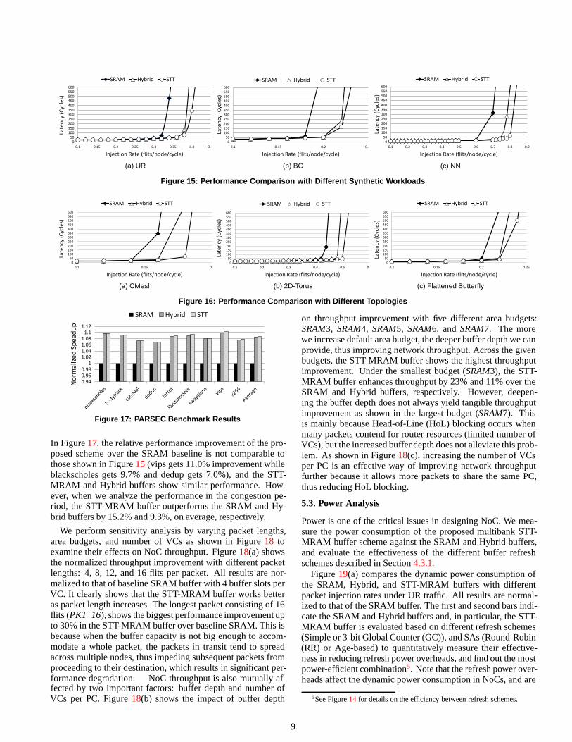
In general, to hiden-cycle write latency, the STT-MRAMbuffer scheme requiresn MUXes forn splitted banks withn−1latches inside a router as shown in Figure12. The increase ofn can negatively affect the performance and area overheads ofthe STT-MRAM buffer. Note thatn is the ratio of the STT-MRAM write latency to the clock cycle time of the NoC clock.As technology advances, we expect the write latency to be re-duced as described in Section2.2, while at the same time theNoC clock frequency increases. Therefore we do not expectnto increase drastically in the near future, hence keeping the pro-posed scheme feasible. In our analysis, whenn stays within 5,we observe negligible performance degradation (less than 1%)with increased extra logic area. The detailed analysis of theimpact of largen is discussed in Section5.4.
Figure9 shows an example data flow for flits from an up-stream router during 3 consecutive clock cycles. Initially, thecontrol of both MUXes, denoted as MUX0 and MUX1, is as-sumed to be set to 0, and all VCs are empty. It is also assumedthat the interconnect clock period is long enough to satisfythesetup and hold constraints of a simple CMOS MUX.• Cycle 0: The input signal of both MUXes is set to 1 (IN1).
Note that, at low loads, flits arrive at the input buffer intermit-tently. In this case, the arriving flit bypasses the input buffer, orunless the buffer is empty, the STT-MRAM buffer directs theflit to either Odd or Even bank based on a one-bit flag indicat-ing the next bank. This ensures that incoming flits are placedin a VC without leaving unused buffer slots in banks. This alsoensures sequential reads by maintaining the FIFO properties ofinput buffers.4.2.2. Read/Write and Refresh LogicUnlike the conventional SRAM input buffer that requires a
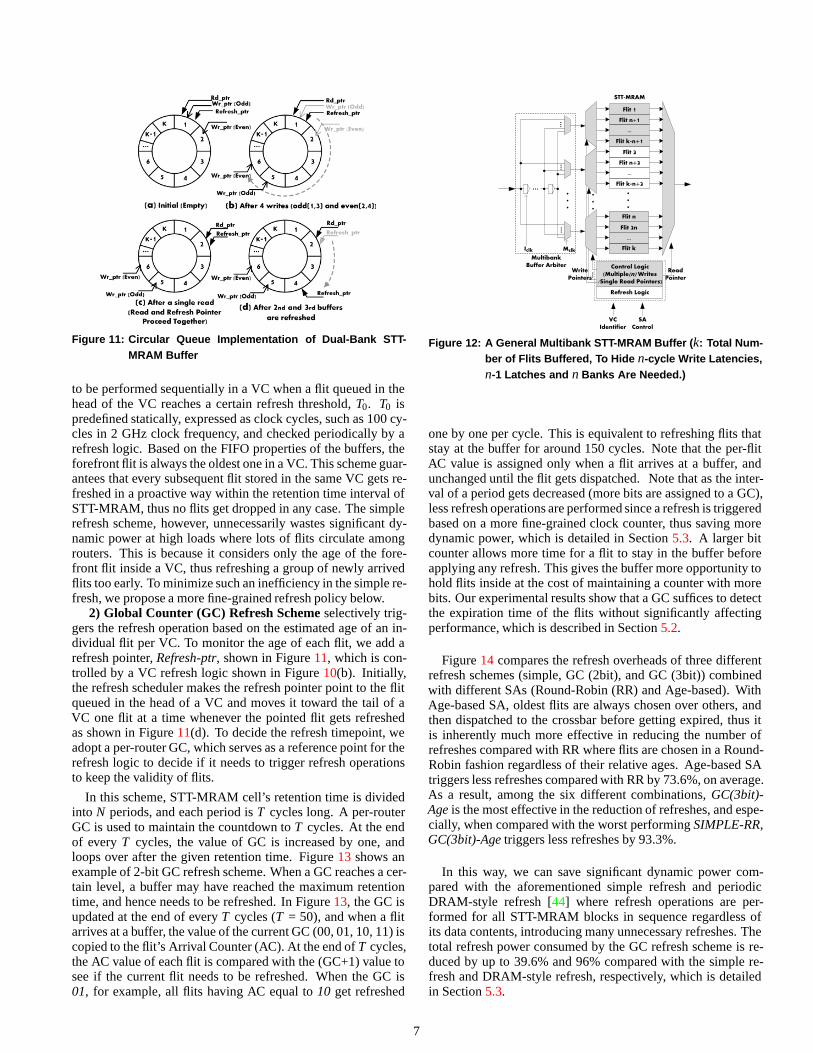
read and a write pointer for read and write operations per VC(Figure 10(a)), the proposed multibank STT-MRAM buffer,assuming 2-cycle write latency, requires dual write pointers,Wr_ptr (Odd)and Wr_ptr (Even), and a single read pointer,Rd_ptr, per VC as shown in Figure10(b). The correspondingVC control logic generates proper read and write pointer valuesfor handling flits in a timely manner. To be specific, initially, asshown in Figure11(a), one of the write pointers,Wr_ptr (Odd),points to the tail of the Odd bank, andWr_ptr (Even)points tothe tail of the Even bank, and the read pointer,Rd_ptr, pointsto the head of the buffer. For a write operation (Figure11(b)),the incoming flit is written to the location pointed by the tailpointer in one of the banks. For a read operation (Figure11(c)),the flit pointed byRd_ptris read out and dispatched to the cross-bar. Note that STT-MRAM read latency is comparable to thatof SRAM and thus no delay occurs for the read operation. Therefresh pointer,Refresh_ptr, shown in Figure11(d), moves ac-cording to the refresh logic which is described in Section4.3.
4.3. Nonvolatility-Relaxed STT-MRAM Buffer
In this section, we propose cost-efficient dynamic buffer refreshschemes to avoid flit dropping, which occurs when flits overstaya given retention time.4.3.1. Dynamic Buffer Refresh SchemesTo avoid flit losses incurred by the relaxed nonvolatility of
STT-MRAM buffers, we employ two different refresh schemes
WritePointer
ReadPointer
SRAM
Control Logic(Write/Read Pointers)
Flit 3
Flit 2
�
Flit K-1
Flit K
Flit 4
VC Identifier
SA Control
Flit 1
ReadPointerControl Logic
(Dual Writes/Single Read Pointers)
Flit 3
Flit 1
Flit K-1
...
Refresh Logic(Refresh Pointer)
Flit 4
Flit 2
Flit K
...
VC Identifier
SA Control
WritePointers
(a) (b)
STT-MRAM
MclkIclk
MultibankBuffer Arbiter
Figure 10: A Baseline SRAM Input Buffer (a) and A Dual-BankSTT-MRAM Input Buffer (b)
through which refresh operations are adaptively triggeredforexpiring flits which almost reach the end of a given retentiontime. Basically, these refresh schemes require an flit-deep re-fresh buffer per each physical channel (PC) forn-cycle writelatency. During a refresh operation, the target flit is read outfrom the input buffer into the refresh buffer, and then writtenback to its original FIFO buffer. If a read request comes be-fore refresh finishes, the flit is directly returned from the refreshbuffer. The refresh buffer is also used as a read buffer to com-pensate forn-cycle write latency of STT-MRAM, and the re-freshes are seamlessly pipelined to allow consecutive refreshes.Note that the refresh buffer can be made using either an exter-nal refresh buffer (ERB) of SRAM, or an internal refresh buffer(IRB) of STT-MRAM. The ERB requires two writes: an initialwrite to the ERB and another subsequent write to the originalFIFO buffer. To decrease such redundant write overheads in theERB, we can relocate the refresh buffer inside the FIFO bufferand when a flit needs to get refreshed, the flit is moved to theIRB, and the IRBs keep progressing through the FIFO bufferas flits get refreshed. Note that the IRB is hidden from the up-stream router to prevent the VA stage in the upstream routerfrom allocating these buffers to flits. It is also noted that theimpact of refresh overheads on the network throughput is negli-gible due to such seamless refresh operations. Also, since flitsarrive at VCs at different points of time, no two flits have thesame timestamp across all VCs in the same PC. Accordingly,we only need a single refresh buffer per PC for the refresh op-eration, and we assume a single flit can be refreshed per cyclein each PC.
1) Simple Refresh Schemeis a straightforward refreshscheduling algorithm, which simply forces a refresh operation
6
Figure 11: Circular Queue Implementation of Dual-Bank STT-MRAM Buffer
to be performed sequentially in a VC when a flit queued in thehead of the VC reaches a certain refresh threshold,T0. T0 ispredefined statically, expressed as clock cycles, such as 100 cy-cles in 2 GHz clock frequency, and checked periodically by arefresh logic. Based on the FIFO properties of the buffers, theforefront flit is always the oldest one in a VC. This scheme guar-antees that every subsequent flit stored in the same VC gets re-freshed in a proactive way within the retention time interval ofSTT-MRAM, thus no flits get dropped in any case. The simplerefresh scheme, however, unnecessarily wastes significantdy-namic power at high loads where lots of flits circulate amongrouters. This is because it considers only the age of the fore-front flit inside a VC, thus refreshing a group of newly arrivedflits too early. To minimize such an inefficiency in the simplere-fresh, we propose a more fine-grained refresh policy below.
2) Global Counter (GC) Refresh Schemeselectively trig-gers the refresh operation based on the estimated age of an in-dividual flit per VC. To monitor the age of each flit, we add arefresh pointer,Refresh-ptr, shown in Figure11, which is con-trolled by a VC refresh logic shown in Figure10(b). Initially,the refresh scheduler makes the refresh pointer point to theflitqueued in the head of a VC and moves it toward the tail of aVC one flit at a time whenever the pointed flit gets refreshedas shown in Figure11(d). To decide the refresh timepoint, weadopt a per-router GC, which serves as a reference point for therefresh logic to decide if it needs to trigger refresh operationsto keep the validity of flits.
In this scheme, STT-MRAM cell’s retention time is dividedinto N periods, and each period isT cycles long. A per-routerGC is used to maintain the countdown toT cycles. At the endof everyT cycles, the value of GC is increased by one, andloops over after the given retention time. Figure13 shows anexample of 2-bit GC refresh scheme. When a GC reaches a cer-tain level, a buffer may have reached the maximum retentiontime, and hence needs to be refreshed. In Figure13, the GC isupdated at the end of everyT cycles (T = 50), and when a flitarrives at a buffer, the value of the current GC (00, 01, 10, 11) iscopied to the flit’s Arrival Counter (AC). At the end ofT cycles,the AC value of each flit is compared with the (GC+1) value tosee if the current flit needs to be refreshed. When the GC is01, for example, all flits having AC equal to10 get refreshed
ReadPointer
Control Logic (Multiple(n) Writes
/Single Read Pointers)
Flit n+2
Flit 2
Flit k-n+2
...
Refresh Logic
Flit 2n
Flit n
Flit k
...
VC Identifier
SA Control
STT-MRAM
WritePointers
. . .
. . .
...
...
Flit n+1
Flit 1
Flit k-n+1
...
MclkIclk
MultibankBuffer Arbiter
......
.... . .
Figure 12: A General Multibank STT-MRAM Buffer ( k: Total Num-ber of Flits Buffered, To Hide n-cycle Write Latencies,n-1 Latches and n Banks Are Needed.)
one by one per cycle. This is equivalent to refreshing flits thatstay at the buffer for around 150 cycles. Note that the per-flitAC value is assigned only when a flit arrives at a buffer, andunchanged until the flit gets dispatched. Note that as the inter-val of a period gets decreased (more bits are assigned to a GC),less refresh operations are performed since a refresh is triggeredbased on a more fine-grained clock counter, thus saving moredynamic power, which is detailed in Section5.3. A larger bitcounter allows more time for a flit to stay in the buffer beforeapplying any refresh. This gives the buffer more opportunity tohold flits inside at the cost of maintaining a counter with morebits. Our experimental results show that a GC suffices to detectthe expiration time of the flits without significantly affectingperformance, which is described in Section5.2.
Figure14 compares the refresh overheads of three differentrefresh schemes (simple, GC (2bit), and GC (3bit)) combinedwith different SAs (Round-Robin (RR) and Age-based). WithAge-based SA, oldest flits are always chosen over others, andthen dispatched to the crossbar before getting expired, thus itis inherently much more effective in reducing the number ofrefreshes compared with RR where flits are chosen in a Round-Robin fashion regardless of their relative ages. Age-basedSAtriggers less refreshes compared with RR by 73.6%, on average.As a result, among the six different combinations,GC(3bit)-Ageis the most effective in the reduction of refreshes, and espe-cially, when compared with the worst performingSIMPLE-RR,GC(3bit)-Agetriggers less refreshes by 93.3%.
In this way, we can save significant dynamic power com-pared with the aforementioned simple refresh and periodicDRAM-style refresh [44] where refresh operations are per-formed for all STT-MRAM blocks in sequence regardless ofits data contents, introducing many unnecessary refreshes. Thetotal refresh power consumed by the GC refresh scheme is re-duced by up to 39.6% and 96% compared with the simple re-fresh and DRAM-style refresh, respectively, which is detailedin Section5.3.
7
0 50 100 150 200 (cycles)
00 01 10 11
Tret Retention time (cycle)
T Refresh Check Interval
(= Tret/2^n)
(Tret = 200, T = 50)
1st
period 2nd
period 3rd
period 4th
period
n-bit GC (n=2)
GC value :
Figure 13: An Example of a 2-bit Global Counter (GC) RefreshLogic (retention time: 100 ns(200 cycles in 2 GHz))
0102030405060708090
100110120
0 0.1 0.2 0.3 0.4 0.5 0.6 0.7
Nu
mb
er
of
Re
fre
sh
(x1
0)
Injection Rate (flits/node/cycle)
SIMPLE-RR GC(2bit)-RR GC(3bit)-RR
SIMPLE-Age GC(2bit)-Age GC(3bit)-AgeSTT-MRAM
Efficiency in Refresh Reduction
- GC(3bit) > GC(2bit) > SIMPLE
- Age > RR
SIMPLE
GC(2bit)
GC(3bit)
Figure 14: Number of Refreshes with Different RefreshSchemes (Simple/GC (2bit/3bit)), and SAs (RR/Age)
5. Performance Evaluation
5.1. System Configuration
A cycle-accurate NoC simulator is used to conduct the de-tailed evaluation of the proposed schemes. It implements thepipelined router architecture with VCs, a VC allocator (VA), aswitch arbiter (SA) and a crossbar. The network is equippedwith 2-stage speculative routers with lookahead routing [17].The router has a set ofvVCs per input port. Each VC contains ak-flit buffer with 16B flit size. In our evaluation, we assume thatv is 4, whilek may vary with different buffer configurations. Adimension order routing, XY, is used with wormhole switchingflow control in an (8x8) 2D-mesh. A variety of synthetic work-loads are used to measure the effectiveness of the STT-MRAMbuffer schemes: uniform random(UR), bit complement(BC)and nearest neighbor(NN). To evaluate the proposed schemesunder realistic environments, we also run PARSEC [3] parallelbenchmarks via the trace readers in Netrace [23] that is incor-porated into our NoC simulator. Table1 specifies the detailedCMP configuration.
To estimate the power, area, and timing of SRAM/STT-MRAM routers operating with 1 V supply voltage in 2 GHzclock frequency, we modified an open source NoC router RTLmodel [2] and synthesized in Synopsys Design Compiler with aTSMC 45nm technology library. SRAM/STT-MRAM param-eter values in Table2 are obtained through the STT-MRAManalyses described in Section2.2 and based on relevant STT-MRAM literatures [20, 27]. Note that the unit of the leakagepower ismW per 1-flit buffer. Throughout this paper, the sizesof the SRAM and STT-MRAM buffers, defined by the num-ber of flits per VC, are denoted bySRAM# andSTT#, respec-tively. As stated in Section2, STT-MRAM basically provides4 times more buffer capacity compared with SRAM under thesame area budget (SRAM4 is equal toSTT16). For the STT-MRAM buffer schemes, however, due to the extra area over-heads incurred by additional circuitry for the MBA shown inFigure8, 2.58% of buffer spaces get sacrificed under 2-cyclewrite latency. Thus, STT-MRAM can provide approximately3.5 times more buffer capacities than the conventional SRAM
Table 1: CMP System Configuration
System Parameters Details
Clock frequency 5 GHz / 2 GHz (Core / NoC)# of processors 64, In-order, Alpha ISA
L1 I and D caches Direct-mapped 32KB (L1I)4-way 32KB (L1D), 3 cycles
Table 2: SRAM and STT-MRAM Parameters with Different Reten-tion Times (The Hybrid Buffer [27] utilizes 10 ms.)
buffer (SRAM4 is equal toSTT14). The detailed area analysisis given in Section5.4.
5.2. Performance Analysis
Figure 15 shows performance results of three different bufferconfigurations: the SRAM buffer, the Hybrid buffer, and theproposed STT-MRAM buffer under UR, BC, and NN trafficpatterns. All results are measured under the same area bud-get,SRAM4 per VC, for input buffers. The Hybrid buffer canaccommodate 7 flits per VC, consisting ofSRAM3 andSTT4,which is an optimal hybrid design suggested in [27], while theSTT-MRAM buffer accommodates 14 flits per VC. In all cases,on average, the STT-MRAM buffer shows better throughput by19.9% for UR, 23.9% for BC, and 21.2% for NN comparedwith the SRAM buffer, and 5.1% compared with the Hybridbuffer across different traffic patterns. These results indicatethat the potential performance degradation caused by the mul-ticycle write latencies of STT-MRAM can be offset by the in-creased buffer size and the proposed multibank STT-MRAMbuffer scheme, thus resulting in significant performance im-provement.
We also evaluate the STT-MRAM buffer under varioustopologies: Concentrated Mesh (CMesh), 2D-Torus, and Flat-tened Butterfly [30]. Figure 16 shows that the STT-MRAMbuffer helps increase throughput in CMesh, 2D-Torus, and Flat-tened Butterfly by 25.9%, 20.2%, and 10% compared with theSRAM buffer, and 5.7%, 9.0%, and 5.2% compared with theHybrid buffer, respectively.
Figure 17 shows speedups relative to the SRAM baselinewith PARSEC benchmarks. We assumeSRAM4 per VC as anarea budget, the same as a cache block size. The average net-work load in PARSEC benchmarks is low, but because they ex-hibit bursty communication and have congestion periods (thetime period when the average ratio of buffer occupancy in in-jection ports is above a threshold, which is set to 75% in ourstudy), our scheme contributes to improve NoC performance.
8
0
50
100
150
200
250
300
350
400
450
500
550
600
0.1 0.15 0.2 0.25 0.3 0.35 0.4 0.45
Late
ncy
(C
ycle
s)
Injection Rate (flits/node/cycle)
SRAM Hybrid STT
(a) UR
0
50
100
150
200
250
300
350
400
450
500
550
600
0.1 0.15 0.2 0.25
Late
ncy
(C
ycle
s)
Injection Rate (flits/node/cycle)
SRAM Hybrid STT
(b) BC
0
50
100
150
200
250
300
350
400
450
500
550
600
0.1 0.2 0.3 0.4 0.5 0.6 0.7 0.8 0.9
Late
ncy
(C
ycle
s)
Injection Rate (flits/node/cycle)
SRAM Hybrid STT
(c) NN
Figure 15: Performance Comparison with Different Syntheti c Workloads
0
50
100
150
200
250
300
350
400
450
500
550
600
0.1 0.15 0.2
Late
ncy
(C
ycle
s)
Injection Rate (flits/node/cycle)
SRAM Hybrid STT
(a) CMesh
0
50
100
150
200
250
300
350
400
450
500
550
600
0.1 0.2 0.3 0.4 0.5 0.6
Late
ncy
(C
ycle
s)
Injection Rate (flits/node/cycle)
SRAM Hybrid STT
(b) 2D-Torus
0
50
100
150
200
250
300
350
400
450
500
550
600
0.1 0.15 0.2 0.25
Late
ncy
(C
ycle
s)
Injection Rate (flits/node/cycle)
SRAM Hybrid STT
(c) Flattened Butterfly
Figure 16: Performance Comparison with Different Topologi es
0.94
0.96
0.98
1
1.02
1.04
1.06
1.08
1.1
1.12
No
rma
lize
d S
pe
ed
up
SRAM Hybrid STT
Figure 17: PARSEC Benchmark Results
In Figure17, the relative performance improvement of the pro-posed scheme over the SRAM baseline is not comparable tothose shown in Figure15 (vips gets 11.0% improvement whileblackscholes gets 9.7% and dedup gets 7.0%), and the STT-MRAM and Hybrid buffers show similar performance. How-ever, when we analyze the performance in the congestion pe-riod, the STT-MRAM buffer outperforms the SRAM and Hy-brid buffers by 15.2% and 9.3%, on average, respectively.
We perform sensitivity analysis by varying packet lengths,area budgets, and number of VCs as shown in Figure18 toexamine their effects on NoC throughput. Figure18(a) showsthe normalized throughput improvement with different packetlengths: 4, 8, 12, and 16 flits per packet. All results are nor-malized to that of baseline SRAM buffer with 4 buffer slots perVC. It clearly shows that the STT-MRAM buffer works betteras packet length increases. The longest packet consisting of 16flits (PKT_16), shows the biggest performance improvement upto 30% in the STT-MRAM buffer over baseline SRAM. This isbecause when the buffer capacity is not big enough to accom-modate a whole packet, the packets in transit tend to spreadacross multiple nodes, thus impeding subsequent packets fromproceeding to their destination, which results in significant per-formance degradation. NoC throughput is also mutually af-fected by two important factors: buffer depth and number ofVCs per PC. Figure18(b) shows the impact of buffer depth
on throughput improvement with five different area budgets:SRAM3, SRAM4, SRAM5, SRAM6, andSRAM7. The morewe increase default area budget, the deeper buffer depth we canprovide, thus improving network throughput. Across the givenbudgets, the STT-MRAM buffer shows the highest throughputimprovement. Under the smallest budget (SRAM3), the STT-MRAM buffer enhances throughput by 23% and 11% over theSRAM and Hybrid buffers, respectively. However, deepen-ing the buffer depth does not always yield tangible throughputimprovement as shown in the largest budget (SRAM7). Thisis mainly because Head-of-Line (HoL) blocking occurs whenmany packets contend for router resources (limited number ofVCs), but the increased buffer depth does not alleviate thisprob-lem. As shown in Figure18(c), increasing the number of VCsper PC is an effective way of improving network throughputfurther because it allows more packets to share the same PC,thus reducing HoL blocking.
5.3. Power Analysis
Power is one of the critical issues in designing NoC. We mea-sure the power consumption of the proposed multibank STT-MRAM buffer scheme against the SRAM and Hybrid buffers,and evaluate the effectiveness of the different buffer refreshschemes described in Section4.3.1.
Figure19(a) compares the dynamic power consumption ofthe SRAM, Hybrid, and STT-MRAM buffers with differentpacket injection rates under UR traffic. All results are normal-ized to that of the SRAM buffer. The first and second bars indi-cate the SRAM and Hybrid buffers and, in particular, the STT-MRAM buffer is evaluated based on different refresh schemes(Simple or 3-bit Global Counter (GC)), and SAs (Round-Robin(RR) or Age-based) to quantitatively measure their effective-ness in reducing refresh power overheads, and find out the mostpower-efficient combination5. Note that the refresh power over-heads affect the dynamic power consumption in NoCs, and are
5See Figure14 for details on the efficiency between refresh schemes.
9
0.90
0.95
1.00
1.05
1.10
1.15
1.20
1.25
1.30
1.35
SRAM STT SRAM STT SRAM STT SRAM STT
PKT_4 PKT_8 PKT_12 PKT_16
No
rma
lize
d T
hro
ug
hp
ut
Packet Length (Flits/Packet)
(a) Different Packet Lengths
0.95
1.00
1.05
1.10
1.15
1.20
1.25
SR
AM
Hy
bri
d
ST
T
SR
AM
Hy
bri
d
ST
T
SR
AM
Hy
bri
d
ST
T
SR
AM
Hy
bri
d
ST
T
SR
AM
Hy
bri
d
ST
T
SRAM3 SRAM4 SRAM5 SRAM6 SRAM7
No
rma
lize
d T
hro
ug
hp
ut
Area Budget (SRAM per VC)
(b) Different Area Budgets
0.95
1.00
1.05
1.10
1.15
1.20
1.25
SRAM STT SRAM STT SRAM STT
VC_4 VC_6 VC_8
No
rma
lize
d T
hro
ug
hp
ut
Number of VCs (per PC)
(c) Different Number of VCs
Figure 18: Sensitivity Analysis (Normalized Throughput Im provement)
Figure 19: Normalized Power Consumption - SRAM/Hybrid/STT -MRAM with Differ-ent Refresh Schemes (Simple/GC(3bit)) and SAs (RR/Age) (Note that STT-MRAM power consumption increases at injection rates (> 0.35) due to theadditional refresh power)
02468
10121416182022
Tota
l P
ow
er
(W)
SRAM Hybrid STT
Figure 20: Total Router Power Consumptionin PARSEC Benchmarks
increasing proportionally to the number of refreshes performed.Thus, to achieve a power-efficient NoC, it is necessary to em-ploy a buffer refresh scheme that triggers less refreshes. In Fig-ure 19(a), the baseline SRAM consumes the least normalizeddynamic power because the Hybrid and STT-MRAM buffersrequire higher write energy compared to that of the SRAM (seeTable2). The Hybrid buffer consumes 1.7 times and 1.4 timesmore dynamic power, on average, compared with the SRAMand STT-MRAM buffers each. This is mostly due to the fre-quent migrations from SRAM to STT-MRAM inside the Hy-brid buffer, and a higher write energy associated with a highre-tention STT-MRAM, 10ms, in the Hybrid buffer, compared tothat of the multibank STT-MRAM buffer. For the STT-MRAMbuffer,GC(3bit)-Ageconsumes the least dynamic power acrossdifferent combinations of refresh schemes. Specifically, com-pared with theSIMPLE-RRand SIMPLE-Age, GC(3bit)-Ageconsumes less dynamic power by 15.4% and 8.0%, respectivelyat high injection rates (> 0.35).
Figure 19(b) compares the total power consumption ofrouters with different buffer schemes. The total router powerincludes dynamic and leakage power of all routers across thenetwork. On average, there is 17% improvement in total routerpower going from baseline SRAM to STT-MRAM buffer de-sign. With our proposed buffer refreshment schemes, althoughthere is an increase in the dynamic power, we consistently ob-serve efficiency in total router power consumption of the pro-posed STT-MRAM buffer. This is attributed to the fact thatthe fraction of dynamic power to the total power is not signif-icant compared to the very high leakage power [29, 54]. Inthis context, due to the power hungry nature of SRAM, theSRAM and Hybrid buffers consume significantly more powerthan the STT-MRAM buffer. Among the three different com-binations of the STT-MRAM refresh schemes,GC(3bit)-Age
consumes less total router power by 8.4% and 14.7%, com-pared with theSIMPLE-RRand baseline SRAM, respectively.Also, the Hybrid scheme consumes 9.8% and 32.5% more totalrouter power, on average, especially at high injection rates (>0.3), compared to the SRAM and STT-MRAM schemes. Thisis because of the migration power overheads, high STT-MRAMwrite energy, and high SRAM leakage power in the Hybridbuffer.
Figure20compares the total router power consumption withPARSEC benchmarks. Among the three different schemes,the STT-MRAM router is the most power-efficient, consuming17.8% and 44.9% less power compared with the SRAM and Hy-brid routers, respectively.Blackscholesconsumes the least to-tal power in the STT-MRAM router by 18.7% and 46.4% com-pared with the SRAM and Hybrid routers.
5.4. Impact of Write Delays of STT-MRAM
For our scheme, STT-MRAM write latency is an important fac-tor affecting the overall NoC area and performance. Till now,in our experiments, we assume STT-MRAM has 2-cycle writedelay with a density of 3.5 times SRAM, but as we increasethe write latency further, the extra logics, such as MUXes andlatches, hiding the multicycle writes need to be added. Due tosuch additional spaces taken up by the extra logics in the STT-MRAM buffer, STT-MRAM is given relatively less area in thegiven buffer space. Specifically, whenn (write delay) equals2, initial single router area, its buffer area (per input port), andextra logic area (per buffer) are 106,709µm2, 14,762µm2 (A),and 689µm2 (B), respectively, where the effective buffer area is14,073µm2 (A-B). As we increasen, while keeping per routerarea budget intact, extra logic area increases by approximately7.5% per additional write latency, thus leading to decreased
10
0
0.5
1
1.5
2
2.5
3
3.5
4
2 3 4 5 6 7 8 9
No
rma
lize
d
ST
T-M
RA
M D
en
sity
STT-MRAM Write Latency
SRAM STT-MRAM
Figure 21: Normalized STT-MRAM Density under the Same Per-Router Area Budget
effective buffer space per input port (Figure21). Across thedifferent write latencies of STT-MRAM (3, 4, and 5), we ob-serve negligible performance degradation (less than 1%) underUR traffic. This is because STT-MRAM still provides enoughbuffer space to sustain the network bandwidth. However, theperformance becomes equal to or less than that of SRAM base-line when the STT-MRAM buffer has similar capacities withthe SRAM buffer due to the reduced density. In our configu-ration, this occurs when the STT-MRAM write latency is 9 ormore cycles.
5.5. Comparison with Other NoC Techniques
There have been a few studies to improve performance withlimited buffer resources in NoC design [39, 36]. We com-pare the power and performance benefits of our scheme withthem. BLESS [39] reduces buffer power and area overheadsby eliminating router buffers, and handles network contentionby deflecting contending flits to any free output port. In ourevaluation, the performance overheads of BLESS outweigh itsgains due to the increased allocator complexities that avoid live-locks, and the extra packet overheads, where flits in a packetcontains routing information to be independently routed tothedestination. BLESS saves significant router area by eliminatingbuffer spaces, but the frequent deflections of BLESS at highloads consume significant dynamic power, and leads to earlynetwork saturation as shown in Figure22. On the other hand,the STT-MRAM router provides higher throughput by 54.1%than that of BLESS, and is more power-efficient at flit injectionrates greater than 22% compared to BLESS. WPF [36] pro-poses a bandwidth-efficient, fully adaptive routing schemeinVC-limited NoCs where short packets dominate. WPF makespackets traverse all minimal paths, thus enhancing routingflexi-bility, and provides deadlock avoidance techniques which allownon-empty VCs to be re-allocated, achieving high VC utiliza-tion. Under the same area budget, as shown in Figure22, underUR traffic, the STT-MRAM router shows better performanceby 8.5% than that of WPF due to the high density buffer prop-erties of STT-MRAM.
6. Related Work
Many prior studies have adopted STT-MRAM to pro-vide power/performance-optimized architectural supports anddensity-optimized secondary storages. Guoet al. [20] detailedSTT-MRAM based architectural techniques to offer power-efficient and scalable microprocessors. Goswamiet al. [19]proposed STT-MRAM based GPGPU architectures and hybridshared memory for power-performance optimizations. In [29,44, 48], the data retention time of STT-MRAM has been care-fully adjusted to achieve better write performance and reduced
0
20
40
60
80
100
0 0.05 0.1 0.15 0.2 0.25 0.3 0.35 0.4
Late
ncy
(C
ycle
s)
Injection Rate (flits/node/cycle)
BLESS SRAM WPF STT
Figure 22: Comparisons with BLESS [ 39] and WPF [ 36] (UR)
write energy for caches in CMPs. However, the cache basedschemes cannot be directly applicable to NoCs since they aredesigned for memories having longer data residence time andlarger capacity compared to FIFO buffers. Power-gating [6]and bufferless NoC [16, 22] have been introduced to reducerouter power consumption. Power-gating is a circuit-leveltech-nique mitigating the static power consumption of NoCs by cut-ting off power temporarily. However, due to frequent statetransitions and unavoidable wakeup time delays, as describedin [6], power-gating rather consumes more power at high load,and has higher average packet latency at both low and highload compared to a non-power-gated NoC, and such overheadsincrease as network scale grows. Bufferless NoC eliminatesbuffers, thus the peak network throughput is reduced, and asstated in [16], it has higher packet latency overall, resulting indegraded performance. Also, although network power is oftensignificantly reduced at low-to-medium load, bufferless NoCconsumes more power as the network becomes congested com-pared to a buffered NoC mostly due to increased link powerfrom frequent deflections. However, in this work we providehigh bandwidth NoC with low power consumption even at highnetwork load using the proposed STT-MRAM NoC router.
7. Other Applications and Future Work
The multibank STT-MRAM buffer scheme can be used inmultiple domains such as instruction queue, reorder buffer,and prefetch buffer. Since instructions are generally usedupquickly, large instruction queues allow for better instructionlevel parallelism [40]. In this context, we will explore usingour scheme as a worthy prospective in terms of power consump-tion and queue length. There are several studies dealing withthe efficiency of reorder buffers [33, 32], and exploring the life-times of variables in programs [35], which show that a largeportion of the variables whose values are held in the reorderbuffers are short lived. This leads to a mixture of variableswithirregular lifetimes. We plan to examine a hybrid SRAM/STT-MRAM buffer scheme which accounts for the variation in re-tention times required. We will explore utilizing STT-MRAMbuffers as an attractive alternative to prefetch buffers [7] for sav-ing power and providing larger buffer space since prefetcheddata do not need to be cached for a long time. We also plan ontackling the challenges of having data retention times tuned tothe timeliness of prefetching so as to make our design feasible.
8. Conclusions
In this paper, we have proposed a novel NoC router input bufferdesign with STT-MRAM, and achieved significant through-put improvement with efficient power consumption. Thehigh density of STT-MRAM facilitates accommodating largerbuffers compared with SRAM under the same area budgets.
11
Through the multibank STT-MRAM buffer design combinedwith power-efficient refresh schemes, the long write latency ofSTT-MRAM is effectively hidden while consuming less power.Simulation results show performance improvement of 21.6%,and 17% savings in the total router power compared with a con-ventional SRAM based NoC router.
References[1] M. Ahn and E. J. Kim, “Pseudo-Circuit: Accelerating Communica-
tion for On-Chip Interconnection Networks,” inProceedings of MICRO,2010.
[2] D. U. Becker, “Efficient Microarchitecture for Network-on-ChipRouters,” inPh.D. Dissertation. Stanford University, 2012.
[3] C. Bienia, S. Kumar, J. P. Singh, and K. Li, “The PARSEC BenchmarkSuite: Characterization and Architectural Implications,” in Proceedingsof PACT, 2008.
[4] Y. Cao, T. Sato, M. Orshansky, D. Sylvester, and C. Hu, “New Paradigmof Predictive MOSFET and Interconnect Modeling for Early CircuitSimulation,” in Proceedings of IEEE Custom Integrated Circuits Con-ference, 2000.
[5] M.-T. Chang, P. Rosenfeld, S.-L. Lu, and B. Jacob, “Technology Com-parison for Large Last-Level Caches: Low-Leakage SRAM, LowWrite-Energy STT-RAM, and Refresh-Optimized eDRAM,” inProceedings ofHPCA, 2013.
[6] L. Chen and T. M. Pinkston, “NoRD: Node-Router Decoupling for Ef-fective Power-gating of On-Chip Routers,” inProceedings of MICRO,2012.
[7] T.-F. Chen and J.-L. Baer, “Effective Hardware-Based Data Prefetchingfor High-Performance Processors,”IEEE Transactions on Computers,vol. 44, pp. 609–623, 1995.
[8] W. J. Dally, “Virtual-Channel Flow Control,”IEEE Trans. Parallel Dis-trib. Syst., vol. 3, pp. 194–205, March 1992.
[9] W. J. Dally and C. L. Seitz, “Deadlock-Free Message Routing in Multi-processor Interconnection Networks,”IEEE Trans. Comput., vol. 36, pp.547–553, May 1987.
[10] D.Bedau, H.Liu, J.-J.Bouzaglou, A.D.Kent, J.Z.Sun, J.A.Katine,E.E.Fullerton, and S.Mangin, “Ultrafast Spin-Transfer Switching inSpin Valve Nanopillars with Perpendicular Anisotropy,”AppliedPhysics Letters, vol. 96, p. 022514, 2010.
[11] Z. Diao, Z. Li, S. Wang, and Y. Ding, “Spin-Transfer Torque Switch-ing in Magnetic Tunnel Junctions and Spin-Transfer Torque RandomAccess Memory,”Journal of Physics:Condensed Matter, vol. 19, p.165209, 2007.
[12] D. DiTomaso, A. Kodi, and A. Louri, “QORE: A fault tolerant network-on-chip architecture with power-efficient quad-function channel (QFC)buffers,” inProceedings of HPCA, 2014.
[13] D. DiTomaso, R. Morris, A. Kodi, A. Sarathy, and A. Louri, “Extendingthe Energy Efficiency and Performance With Channel Buffers,Cross-bars, and Topology Analysis for Network-on-Chips,”IEEE Transactionson VLSI, vol. 21, pp. 2141–2154, 2013.
[14] X. Dong, C. Xu, Y. Xie, and N. P. Jouppi, “NVSim: A Circuit-Level Per-formance, Energy, and Area Model for Emerging Nonvolatile Memory,”in IEEE Transactions on CAD, 2012.
[15] A. Driskill-Smith, D. Apalkov, V. Nikitin, X. Tang, S. Watts, D. Lottis,K. Moon, A. Khvalkovskiy, R. Kawakami, X. Luo, A. Ong, E. Chen,and M. Krounbi, “Latest Advances and Roadmap for In-Plane and Per-pendicular STT-RAM,” inProceedings of IMW, 2011.
[16] C. Fallin, C. Craik, and O. Mutlu, “CHIPPER: A Low-complexityBufferless Deflection Router,” inProceedings of HPCA, 2011.
[17] M. Galles, “Scalable Pipelined Interconnect for Distributed EndpointRouting: The SGI SPIDER Chip,” inProceedings of Hot Interconnect 4,2009.
[18] C. Gómez, M. E. Gómez, P. López, and J. Duato, “Reducing PacketDropping in a Bufferless NoC,” inProceedings of Euro-Par, 2008.
[19] N. Goswami, B. Cao, and T. Li, “Power-performance Co-optimization ofThroughput Core Architecture using Resistive Memory,” inProceedingsof HPCA, 2013.
[20] X. Guo, E. Ipek, and T. Soyata, “Resistive Computation:Avoiding thePower Wall with Low-Leakage, STT-MRAM Based Computing,” inProceedings of ISCA, 2010.
[21] D. Harris,Skew-Tolerant Circuit Design. Morgan Kaufmann, 2000.[22] M. Hayenga, N. E. Jerger, and M. Lipasti, “SCARAB: A Single Cycle
Adaptive Routing and Bufferless Network,” inProceedings of MICRO,2009.
[23] J. Hestness, B. Grot, and S. W. Keckler, “Netrace: Dependency-DrivenTrace-Based Network-on-Chip Simulation,” inProceedings of NoCArc,2010.
[24] Y. Ho, G. M. Huang, and P. Li, “Nonvolatile Memristor Memory: De-vice Characteristics and Design Implications,” inProceedings of ICCAD,2009.
[25] Y. Hoskote, S. Vangal, B. N. Singh, Avind, and S. Borkar,“A 5-GHzMesh Interconnect for a Teraflops Processor,” inProceedings of MICRO,2007.
[27] H. Jang, B. S. An, N. Kulkarni, K. H. Yum, and E. J. Kim, “A HybridBuffer Design with STT-MRAM for On-Chip Interconnects,” inPro-ceedings of NOCS, 2012.
[28] L. Jiang, B. Zhao, Y. Zhang, J. Yang, and B. R. Childers, “ImprovingWrite Operations in MLC Phase Change Memory,” inProceedings ofHPCA, 2012.
[29] A. Jog, A. K. Mishra, C. Xu, Y. Xie, N. Vijaykrishnan, R. Iyer, andC. R. Das, “Cache Revive: Architecting Volatile STT-RAM Caches forEnhanced Performance in CMPs,” inProceedings of DAC, 2012.
[30] J. Kim, J. Balfour, and W. Dally, “Flattened Butterfly Topology for On-Chip Networks,” inProceedings of MICRO, 2007.
[31] A. K. Kodi, A. Sarathy, and A. Louri, “iDEAL: Inter-Router Dual-Function Energy and Area-Efficient Links for Network-on-Chip (NoC)Architectures,” inProceedings of ISCA, 2008.
[32] G. Kucuk, D. Ponomarev, O. Ergin, and K. Ghose, “Reducing ReorderBuffer Complexity Through Selective Operand Caching,” inProceed-ings of ISLPED, 2003.
[33] G. Kucuk, D. Ponomarev, and K. Ghose, “Low- Complexity ReorderBuffer Architecture,” inProceedings of ICS, 2002.
[34] A. Kumar, L.-S. Peh, and N. Jha, “Token Flow Control,” inProceedingsof MICRO, 2008.
[35] L. A. Lozano C. and G. R. Gao, “Exploiting Short-Lived Variables inSuperscalar Processors,” inProceedings of MICRO, 1995.
[36] S. Ma, N. E. Jerger, and Z. Wang, “Whole Packet Forwarding: EfficientDesign of Fully Adaptive Routing Algorithms for Networks-on-chip,” inProceedings of HPCA, 2012.
[37] G. Michelogiannakis, D. Sanchez, W. J. Dally, and C. Kozyrakis, “Eval-uating Bufferless Flow Control for On-Chip Networks,” inProceedingsof NOCS, 2010.
[38] A. K. Mishra, X. Dong, G. Sun, Y. Xie, N. Vijaykrishnan, and C. R. Das,“Architecting On-Chip Interconnects for Stacked 3D STT-RAM Cachesin CMPs,” inProceedings of ISCA, 2011.
[39] T. Moscibroda and O. Mutlu, “A Case for Bufferless Routing in On-chipNetworks,” inProceedings of ISCA, 2009.
[40] S. E. Raasch, N. L. Binkert, and S. K. Reinhardt, “A Scalable Instruc-tion Queue Design Using Dependence Chains,” inProceedings of ISCA,2002.
[41] A. Raychowdhury, D. Somasekhar, and T. Karnik, “DesignSpace andScalability Exploration of 1T-1STT MTJ Memory Arrays in thePres-ence of Variability and Disturbances,” inProceedings of IEDM, 2009.
[42] N. D. Rizzo, M. DeHerrera, J. Janesky, B. Engel, J. Slaughter, andS. Tehrani, “Thermally Activated Magnetization Reversal in SubmicronMagnetic Tunnel Junctions for Magnetoresistive Random Access Mem-ory,” Applied Physics Letters, vol. 80, p. 2335, 2002.
[43] C. W. Smullen and S. Gurumurthi, “Designing Giga-ScaleMemory Sys-tems with STT-RAM,” inPh.D. Dissertation, 2011.
[44] C. W. Smullen, V. Mohan, A. Nigam, S. Gurumurthi, and M. R.Stan, “Relaxing Non-Volatility for Fast and Energy-Efficient STT-RAMCaches,” inProceedings of HPCA, 2011.
[45] G. Sun, X. Dong, Y. Xie, J. Li, and Y. Chen, “A Novel Architecture ofthe 3D Stacked MRAM L2 Cache for CMPs,” inProceedings of HPCA,2009.
[46] G. Sun, E. Kursun, and Y. Xie, “Exploring the Vulnerability of CMPs toSoft Errors with 3D Stacked Non-Volatile Memory,” inProceedings ofICCD, 2011.
[47] H. Sun, C. Liu, W. Xu, and J. Zhao, “Using Magnetic RAM to BuildLow-Power and Soft Error-Resilient L1 Cache,” inIEEE Transactionson VLSI, 2012.
[48] Z. Sun, X. Bi, H. H. Li, W.-F. Wong, Z.-L. Ong, X. Zhu, and W. Wu,“Multi Retention Level STT-RAM Cache Designs with a DynamicRe-fresh Scheme,” inProceedings of MICRO, 2011.
[49] K. Swaminathany, R. Mukundrajany, N. Soundararajan, andV. Narayanan, “Towards Resilient Micro-Architectures: DatapathReliability Enhancement using STT-MRAM,” inProceedings of ISVLSI,2011.
[50] T.Dunn and A.Kamenev, “Optimization of the Current Pulse for Spin-Torque Switches,”Applied Physics Letters, vol. 98, p. 143109, 2011.
[51] H. Wang, L.-S. Peh, and S. Malik, “Power-driven Design of Router Mi-croarchitectures in On-chip Networks,” inProceedings of MICRO, 2003.
12
[52] Z. Wang, D. A. Jimenez, C. Xu, G. Sun, and Y. Xie, “Adaptive Place-ment and Migration Policy for an STT-RAM-Based Hybrid Cache,” inProceedings of HPCA, 2014.
[53] W.J.Dally and B.Towles,Principles and Practices of InterconnectionNetworks. Morgan Kaufmann, 2003.
[54] X. Wu, J. Li, L. Zhang, E. Speight, R. Rajamony, and Y. Xie, “HybridCache Architecture with Disparate Memory Technologies,” in Proceed-ings of ISCA, 2009.
[55] A. V. Yakovlev, A. M. Koelmans, and L. Lavagno, “High-Level Mod-eling and Design of Asynchronous Interface Logic,”IEEE Design andTest of Computers, vol. 12, pp. 32–40, 1995.
[56] T. T. Ye, L. Benini, and G. D. Micheli, “Analysis of PowerConsumptionon Switch Fabrics in Network Routers,” inProceedings of DAC, 2002.