33
© 2015 TechSearch International, Inc. www.techsearchinc.com Changing Packaging Trends and the Impact on Test E. Jan Vardaman, President and Founder

© 2015 TechSearch International, Inc.w w w . t e c h s e a r c h i n c . c o m
Changing Packaging Trends and the Impact on Test
E. Jan Vardaman, President and Founder
© 2016 TechSearch International, Inc.www.techsearchinc .com
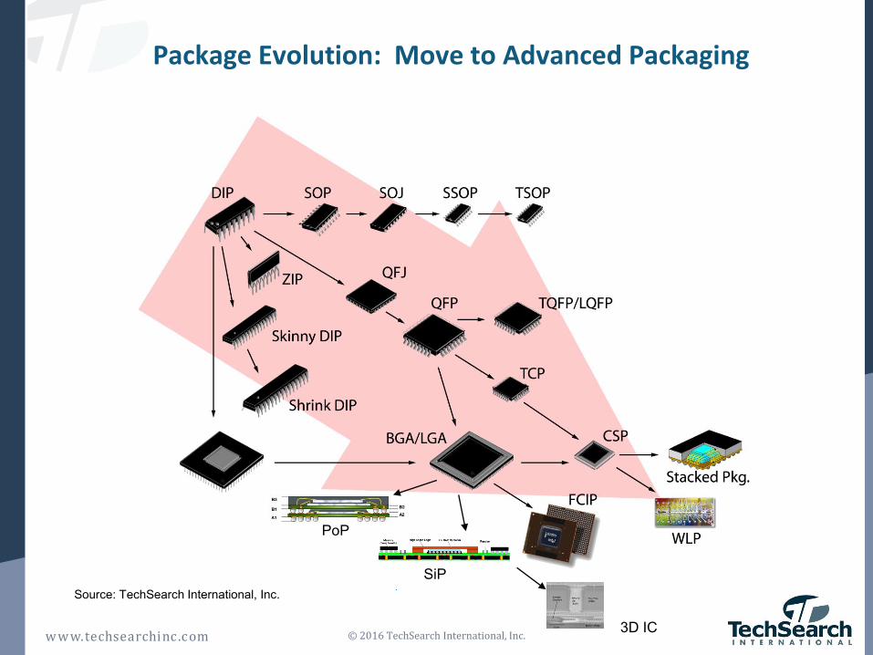
Package Evolution: Move to Advanced Packaging
PoP
SiP
3D IC
Source: TechSearch International, Inc.
© 2016 TechSearch International, Inc.www.techsearchinc .com
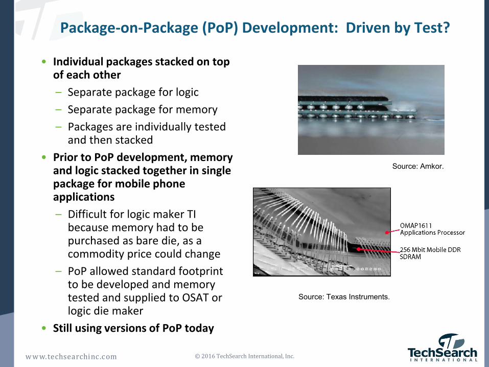
Package-on-Package (PoP) Development: Driven by Test?
• Individual packages stacked on top of each other– Separate package for logic– Separate package for memory– Packages are individually tested
and then stacked• Prior to PoP development, memory
and logic stacked together in single package for mobile phone applications– Difficult for logic maker TI
because memory had to be purchased as bare die, as a commodity price could change
– PoP allowed standard footprint to be developed and memory tested and supplied to OSAT or logic die maker
• Still using versions of PoP today
Source: Amkor.
Source: Texas Instruments.

© 2016 TechSearch International, Inc.www.techsearchinc .com
Connected World: Driving New Package Options
• Healthcare• Sports and fitness• Industrial automation• Automotive electronics• Security for home, office,
industry, etc.• Home automation• Entertainment• Transportation• Energy production

© 2016 TechSearch International, Inc.www.techsearchinc .com
Smartphones Control Connected Devices
• Smartphones play a key role– Tool with diverse wireless connectivity and sensors– Pressure on package design and cost
• Connecting with cars for safer driving– Hands- and eyes-free communication– Navigation and traffic flow– Driving pattern detection– OBD data and alerts
• Industrial and enterprise leveraging consumer technologies and vast smartphone installed base– Real-time process and production monitoring– System diagnostics and configuration– Business interaction in retail space
• Medical products using signal to smartphone for body monitoring
• Home security control and energy monitoring
Source: BMW.
Source: Siemens.
Source: Samsung.
Source: Numerex.
© 2016 TechSearch International, Inc.www.techsearchinc .com
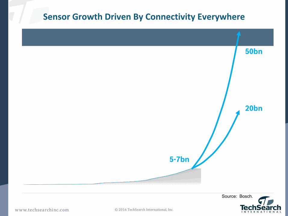
Sensor Growth Driven By Connectivity Everywhere
Source: Bosch.

© 2016 TechSearch International, Inc.www.techsearchinc .com
Wearable Products
• Health and fitness tracking bands including pedometers
• Watch products• More fashionable device to provide monitoring of
elderly patients– Monitor blood pressure– Levels of hydration
• Contain many sensors to accurately calculate– Heart rate– Blood pressure (need higher accuracy) and blood
flow– Glucose levels– Pulse, motion sensing, etc.
Source: Apple..
Source: TPSS..
© 2016 TechSearch International, Inc.www.techsearchinc .com
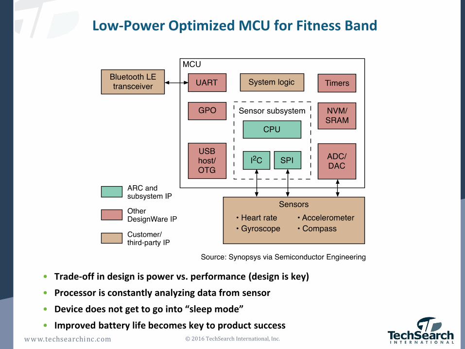
Low-Power Optimized MCU for Fitness Band
• Trade-off in design is power vs. performance (design is key)• Processor is constantly analyzing data from sensor• Device does not get to go into “sleep mode”• Improved battery life becomes key to product success

© 2016 TechSearch International, Inc.www.techsearchinc .com
SiP Key for Connected Smart Systems and Wearables
Connected smart systems require new competences
Source: Bosch.
© 2016 TechSearch International, Inc.www.techsearchinc .com
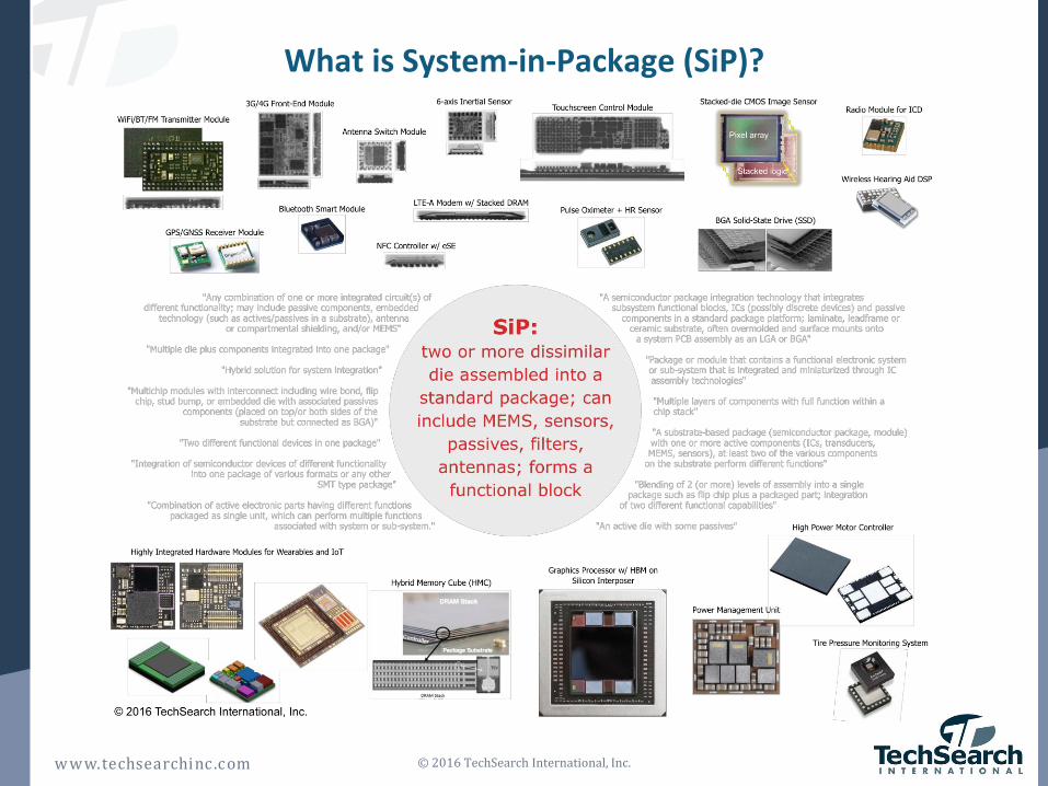
What is System-in-Package (SiP)?

© 2016 TechSearch International, Inc.www.techsearchinc .com
Many Drivers for SiP
• Miniaturization—form factor such as package height, footprint• Heterogeneous technology integration—different device types such
as RF, analog, memory• Mixed process technology assembly—die fabricated on different
silicon technology nodes• System performance and optimization—improved signal integrity,
reduced power consumption• System flexibility, features, and re-configurability• Simplification of module level test and qualification• Total system cost reduction due to reduced system BOM and
complexity, simplified product board, board layer count reduction, reduced development cost, faster time-to-market

© 2016 TechSearch International, Inc.www.techsearchinc .com
Many Formats for SiP…
• Land grid array (LGA)• Ball grid array (BGA)
– Wire bond– Flip chip
• Fine pitch BGA (FBGA) or Laminate CSP– Wire bond – Flip chip
• Fan-out WLP (FO-WLP)– Multiple die with passives
• May include WLPs inside– Broadcom WLP in Murata WiFi module
• Leadframe packages– Routable QFN– MIS-BGA
• Ceramic substrate packages (CLGA)• Silicon interposers for high-performance
systems
LGA module
BGA
FO-WLP
Routable QFN
© 2016 TechSearch International, Inc.www.techsearchinc .com
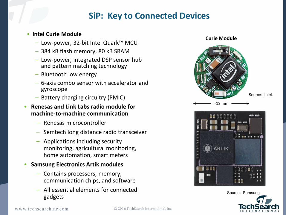
SiP: Key to Connected Devices
• Intel Curie Module – Low-power, 32-bit Intel Quark™ MCU– 384 kB flash memory, 80 kB SRAM– Low-power, integrated DSP sensor hub
and pattern matching technology– Bluetooth low energy– 6-axis combo sensor with accelerator and
gyroscope– Battery charging circuitry (PMIC)
• Renesas and Link Labs radio module for machine-to-machine communication
– Renesas microcontroller– Semtech long distance radio transceiver– Applications including security
monitoring, agricultural monitoring, home automation, smart meters
• Samsung Electronics Artik modules– Contains processors, memory,
communication chips, and software– All essential elements for connected
gadgetsSource: Samsung.
Source: Intel.
Curie Module
≈18 mm

© 2016 TechSearch International, Inc.www.techsearchinc .com
TDK’s Tiny Bluetooth Low Energy Module forSmart Watches and Other Wearables
• Bluetooth low-energy module with IC embedded into thin substrate, peripheral circuitry includes quartz resonator, bandpass filter, and capacitors on the top
• Package size of 4.6 mm x 5.6 mm x 1.0 mm• 65% smaller than individual discrete components
Source: TDK.
© 2016 TechSearch International, Inc.www.techsearchinc .com
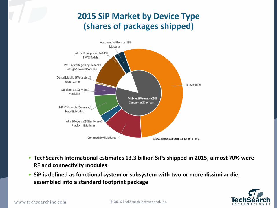
2015 SiP Market by Device Type(shares of packages shipped)
• TechSearch International estimates 13.3 billion SiPs shipped in 2015, almost 70% were RF and connectivity modules
• SiP is defined as functional system or subsystem with two or more dissimilar die, assembled into a standard footprint package
RF�Modules
Connectivity�Modules
APs,�Modems�&�Hardware�Platform�Modules
MEMS�Inertial�Sensors,�Hubs�&�Nodes
Stacked-CIS�Camera�Modules
Other�Mobile,�Wearable�&�Consumer
PMUs,�Voltage�Regulators�&�High�Power�Modules
Silicon�Interposers�&�3D�TSV�DRAMs
Automotive�Sensors�&�Modules
Mobile,�Wearable�&�
Consumer�Devices
©�2016�TechSearch�International,�Inc.

© 2016 TechSearch International, Inc.www.techsearchinc .com
RF SiP: Complex Design = Complex Text Requirements
• RF modules are a complex design that requires comprehensive test strategy
• RF modules typically contain amplifiers, switches, filters, passives, and antennas
• Heterogeneous mix of semiconductor technologies such as GaAs, GaN, SiGe, CMOS, SOI, and/or SOS
• EMI shielding typically conformal, but compartmental is emerging• Typically packaged in LGA
Avago PA module includes FBAR4.4 x 4.25 x 0.88mm FLGA with 18 pads
Murata WiFi 802.11/ Bluetooth / FM Radio module9.8 x 7.5mm LGA with 58 pads
© 2016 TechSearch International, Inc.www.techsearchinc .com
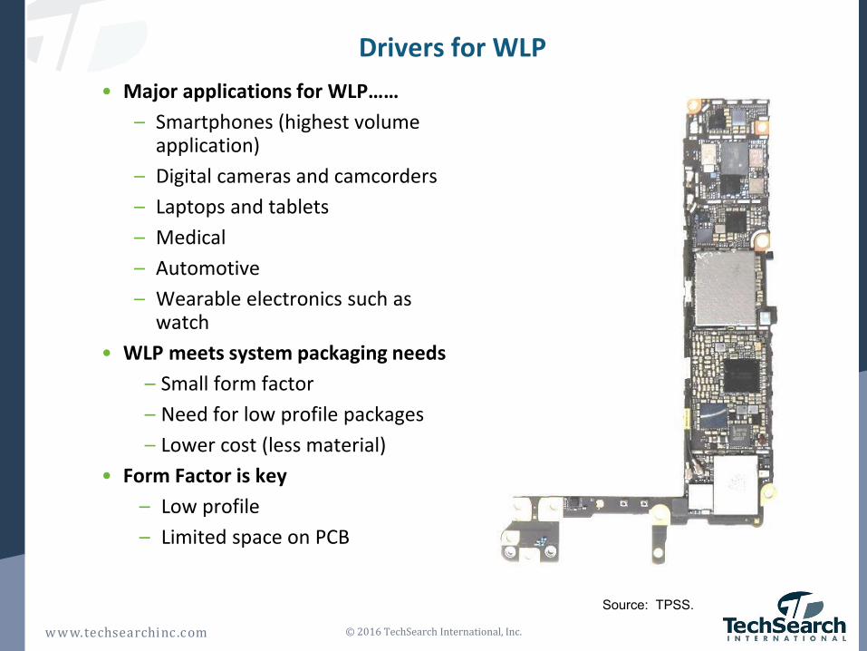
Drivers for WLP• Major applications for WLP……
– Smartphones (highest volume application)
– Digital cameras and camcorders– Laptops and tablets– Medical– Automotive– Wearable electronics such as
watch• WLP meets system packaging needs
– Small form factor– Need for low profile packages– Lower cost (less material)
• Form Factor is key– Low profile– Limited space on PCB
Source: TPSS.
© 2016 TechSearch International, Inc.www.techsearchinc .com
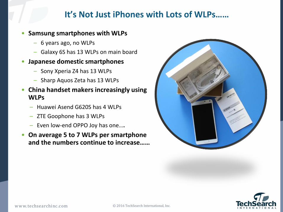
It’s Not Just iPhones with Lots of WLPs……
• Samsung smartphones with WLPs– 6 years ago, no WLPs – Galaxy 6S has 13 WLPs on main board
• Japanese domestic smartphones– Sony Xperia Z4 has 13 WLPs– Sharp Aquos Zeta has 13 WLPs
• China handset makers increasingly using WLPs– Huawei Asend G620S has 4 WLPs– ZTE Goophone has 3 WLPs– Even low-end OPPO Joy has one….
• On average 5 to 7 WLPs per smartphone and the numbers continue to increase……

© 2016 TechSearch International, Inc.www.techsearchinc .com
Conventional WLP Applications• Conventional WLPs for many device types (analog,
digital, sensor, discrete)– Power management IC (PMIC)– Audio CODEC – RF– IPD, ESD protection, filter– LED driver– Electronic compass– Controller– MOSFET – CMOS image sensors– Ambient light sensors– EEPROM
• Conventional WLPs trends– Highest I/O counts and largest body size PMICs– Increasing number of 0.4mm pitch parts, some
0.35mm pitch– Fine pitch parts need high-density PCB to route
signals
Source: ASE.

© 2016 TechSearch International, Inc.www.techsearchinc .com
Wafer Fab
Ball Mount
Laser Mark
Singulation
Wafer Mount
Pick & Place
Drop Ship
Optical Inspection
PI / UBM
Optical Inspection
Bump Wafer Probing
Sawn Wafer Probing
Tape & Reel
Optical Inspection
Option 2
Option 3
Back Grinding
Pre-Bump Probing Option 1
1. Bumping
2. TEST
3. WLCSP Backend
WLP Process Flow (Conventional Fan-in)
Source: OSAT.

© 2016 TechSearch International, Inc.www.techsearchinc .com
Fan-In and Fan-Out WLP Compared
Conventional WLP (Fan-In) Fan-Out WLP (packagefootprint larger than die)
Source: STATS ChipPAC

© 2016 TechSearch International, Inc.www.techsearchinc .com
FO-WLP• Smaller form factor, lower profile package
– Similar to conventional WLP in profile (can be ≤0.4 mm)– No substrate
• Support increased I/O density– Fine L/S (10/10µm) – Roadmaps for <5/5µm L/S, future 2/2µm L/S
• Split die package or multi-die package/SiP– Multiple die in package possible– Die fabricated from different technology nodes can be
assembled in a single package– Can integrate passives
• SiP applications– Radar modules for automotive electronics– Connectivity modules for smart home
Source: STATS ChipPAC.
Source: Freescale Semiconductor.

© 2016 TechSearch International, Inc.www.techsearchinc .com
Applications for FO-WLP
• Baseband processors (in production many years)
• RF transceivers, switch, etc.• Power management integrated circuits
(PMIC)• Connectivity• Radar module for automotive • Near field communication (NFC)• Audio CODEC• Security devices• Microcontrollers• Memory (top PoP)• NAND memory controllers• Application processors• Many multi-die configurations
NXP Radar Module
Source: NXP.
Intel Wireless Division LTE analog baseband5.32 x 5.04 x 0.7mm eWLB127 balls, 0.4mm pitch
Source: TPSS.Marvell PMIC & Audio CODEC
Source: Nanium.

© 2016 TechSearch International, Inc.www.techsearchinc .com
Potential RF, PMIC, CODEC and AP, Migration to FO-WLP
PMIC WLP-94Qualcomm
PM8019
RFIC WLP-164Qualcomm WTR1625L
*Audio codec
WLP-42Cirrus 338S1201
RFIC WLP-66Qualcomm WFR1620
PMIC FCBGA-267
Dialog 338S1251
WiFi/BT/FMFLGA-58
Murata 343S0694
PMIC WLP-28Qualcomm
QFE1100
Modem FCBGA-333Qualcomm MDM9625M
M8 Co-pro. WLP-40NXP
LPC18B1UK
A-CPU PoP-1155Apple/TSMC
APQL-
Source: TPSS.
*
*
*
*
*

© 2016 TechSearch International, Inc.www.techsearchinc .com
Application Processor Packaging Trends: FO-WLP• Thinner package and smaller footprint
– Today 1.0mm height requirement– Future ≤0.8 mm
• 3D IC with TSV provides the ultimate in package height reduction, best electrical performance, but continues to be pushed out (thermal, cost, business issues)
• Silicon interposers too expensive for many mobile products
• PoP in high-end smartphones– Option 1: Continue with FC on thin
substrate– Option 2: Embedded AP in bottom
laminate substrate – Option 3: Fan-out WLP with
application processor as bottom package
– Option 4: Some new format (RDL first/chip last, SWIFT, etc.)
Today’s PoP (1.0mm)
FO-WLP as Bottom PoP (<0.8mm)

© 2016 TechSearch International, Inc.www.techsearchinc .com
Why is FO-WLP A Disruptive Technology?
• No substrate– Thin-film metallization used for
substrate (can go below 5µm L/S)– No traditional laminate substrate
(most application processors had been using laminate substrate with flip chip bump interconnect)
– No traditional underfill – Removes substrate supplier as design
partner• Infrastructure changes
– All packaging can take place at the foundry
– Assembly can also take place at OSAT but uses a non-traditional OSAT assembly line
– Requires IC/package co-design– Moving forward, test has to be done
while still in wafer format
Source: Nanium.
© 2016 TechSearch International, Inc.www.techsearchinc .com
How to Achieve Cost Reduction with FO-WLP?
• Customers demand continuous cost reduction– Lower ASP for semiconductor devices– Lower assembly prices for OSATs
• Is some form of die-last process the answer?
• Is panel processing the answer?• Is 450mm reconstituted wafer the
answer? • How do we test?

© 2016 TechSearch International, Inc.www.techsearchinc .com
Amkor’s SWIFT™
• Target Markets– Mobile, Networking
– BB, AP, Logic + Memory, Deconstructed SoC
• Utilizes Existing Bump and Assembly Capability
– Polymer based
– Flexible• Multi-die and large die capability
• Large package body capability
– Advanced die integration• Stepper capability down to 2um line/space
• Die shift / orthogonal rotation elimination
• Down to 30um in-line copper pillar pitch
– 3D capability• Package stack capability
using Cu pillars or TMV
SWIFTTM Single Die Overmold
SWIFTTM 2 Die Overmold
SWIFTTM 2 Die Exposed
SWIFTTM 2 Die TMV PoP Overmold
SWIFTTM 2 Die Fan-in PoP
© 2016 TechSearch International, Inc.www.techsearchinc .com
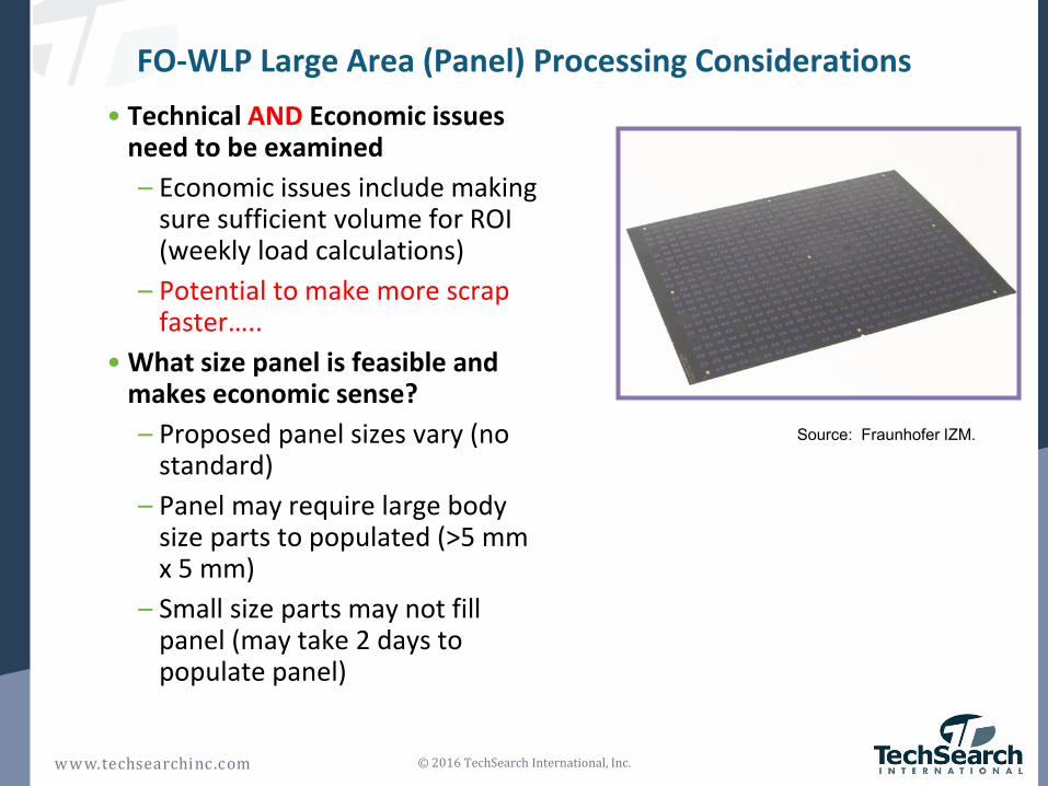
FO-WLP Large Area (Panel) Processing Considerations• Technical AND Economic issues
need to be examined– Economic issues include making
sure sufficient volume for ROI (weekly load calculations)
– Potential to make more scrap faster…..
• What size panel is feasible and makes economic sense?– Proposed panel sizes vary (no
standard)– Panel may require large body
size parts to populated (>5 mm x 5 mm)
– Small size parts may not fill panel (may take 2 days to populate panel)
Source: Fraunhofer IZM.

© 2016 TechSearch International, Inc.www.techsearchinc .com
FO-WLP Large Area (Panel) Processing Considerations
• Dielectric dispense methods?– Spin coat? Other methods such as
dry film lamination, slot coat, etc.– Need inspection for even coating?
• Molding materials and process?– Low CTE material– Low process temperature (higher
process temperature = more moving around)
• Metal plating– Metal to dielectric interface (what
inspection requirements?)– How to sputter seed layer?
• Interconnect reliability? • Inspection for broken metal traces etc.
© 2016 TechSearch International, Inc.www.techsearchinc .com
FO-WLP Large Area (Panel) Processing Considerations
• Assembly of die on panel– Die placement accuracy may be more
difficult to control with large panels (size matters)
– Large area bonders may be required (depending in the size of the panel)
– Throughput (time required to pick and place die in panel)
– How is placement accuracy impacted by tape and mold compound?
– What level of inspection is required to verify accuracy? What speed?
• Singulation method? • Solder ball placement and inspection
method?• How do we test in large panel?
– Back to singulated package test?– Some new test method?
© 2016 TechSearch International, Inc.www.techsearchinc .com
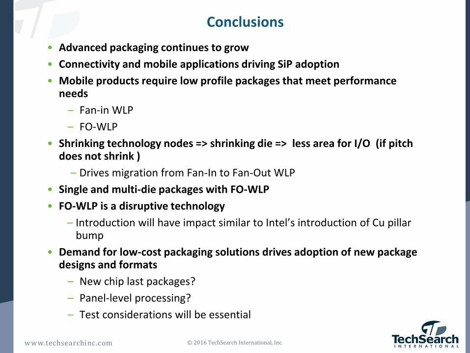
Conclusions• Advanced packaging continues to grow• Connectivity and mobile applications driving SiP adoption• Mobile products require low profile packages that meet performance
needs– Fan-in WLP– FO-WLP
• Shrinking technology nodes => shrinking die => less area for I/O (if pitch does not shrink )
– Drives migration from Fan-In to Fan-Out WLP • Single and multi-die packages with FO-WLP• FO-WLP is a disruptive technology
– Introduction will have impact similar to Intel’s introduction of Cu pillar bump
• Demand for low-cost packaging solutions drives adoption of new package designs and formats
– New chip last packages?– Panel-level processing?– Test considerations will be essential

TechSearch International, Inc.4801 Spicewood Springs Road, Suite 150
Austin, Texas 78759 USA+1.512.372.8887
© 2015 TechSearch International, Inc.w w w . t e c h s e a r c h i n c . c o m
Thank you!


