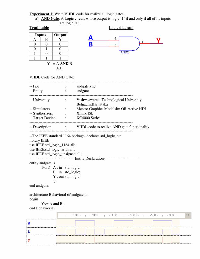
Experiment 1: Write VHDL code for realize all logic gates. a) AND Gate : A Logic circuit whose output is logic ‘1’ if and only if all of its inputs are logic ‘1’. Truth table Logic diagram Y = A AND B = A.B VHDL Code for AND Gate: ------------------------------------------------------------------------------- -- File : andgate.vhd -- Entity : andgate ------------------------------------------------------------------------------- -- University : Vishweswaraia Technological University Belgaum,Karnataka -- Simulators : Mentor Graphics Modelsim OR Active HDL -- Synthesizers : Xilinx ISE -- Target Device : XC4000 Series ------------------------------------------------------------------------------- -- Description : VHDL code to realize AND gate functionality ------------------------------------------------------------------------------- --The IEEE standard 1164 package, declares std_logic, etc. library IEEE; use IEEE.std_logic_1164.all; use IEEE.std_logic_arith.all; use IEEE.std_logic_unsigned.all; ---------------------------------- Entity Declarations ------------------------- entity andgate is Port( A : in std_logic; B : in std_logic; Y : out std_logic ); end andgate; architecture Behavioral of andgate is begin Y<= A and B ; end Behavioral; Inputs Output A B Y 0 0 0 0 1 0 1 0 0 1 1 1 AND2 1 2 3 A Y B a b y ns 500 1000 1500 2000 2500 3000
Transcript
Experiment 1: Write VHDL code for realize all logic gates. a) AND Gate: A Logic circuit whose output is logic ‘1’ if and only if all of its inputs
are logic ‘1’. Truth table Logic diagram
Y = A AND B = A.B VHDL Code for AND Gate: ------------------------------------------------------------------------------- -- File : andgate.vhd -- Entity : andgate ------------------------------------------------------------------------------- -- University : Vishweswaraia Technological University Belgaum,Karnataka -- Simulators : Mentor Graphics Modelsim OR Active HDL -- Synthesizers : Xilinx ISE -- Target Device : XC4000 Series ------------------------------------------------------------------------------- -- Description : VHDL code to realize AND gate functionality ------------------------------------------------------------------------------- --The IEEE standard 1164 package, declares std_logic, etc. library IEEE; use IEEE.std_logic_1164.all; use IEEE.std_logic_arith.all; use IEEE.std_logic_unsigned.all; ---------------------------------- Entity Declarations ------------------------- entity andgate is Port( A : in std_logic; B : in std_logic; Y : out std_logic ); end andgate; architecture Behavioral of andgate is begin Y<= A and B ; end Behavioral;
Inputs Output A B Y 0 0 0 0 1 0 1 0 0 1 1 1
AND2
12
3
A YB
a
b
y
ns500 1000 1500 2000 2500 3000
b)OR Gate: A logic gate whose output is logic ‘0’ if and only if all of its inputs are logic ‘0’.
Truth table Logic diagram
Y = A OR B = A + B VHDL Code for OR Gate: ------------------------------------------------------------------------------- -- File : orgate.vhd -- Entity : orgate ------------------------------------------------------------------------------- -- University : Vishweswaraia Technological University Belgaum,Karnataka -- Simulators : Mentor Graphics Modelsim OR Active HDL -- Synthesizers : Xilinx ISE -- Target Device : XC4000 Series ------------------------------------------------------------------------------- -- Description : VHDL code to realize OR gate functionality ------------------------------------------------------------------------------- --The IEEE standard 1164 package, declares std_logic, etc. library IEEE; use IEEE.std_logic_1164.all; use IEEE.std_logic_arith.all; use IEEE.std_logic_unsigned.all; ---------------------------------- Entity Declarations ------------------------- entity orgate is Port( A : in std_logic; B : in std_logic; Y : out std_logic ); end orgate; architecture Behavioral of orgate is begin Y<= A or B ; end Behavioral;
Inputs Output A B Y 0 0 0 0 1 1 1 0 1 1 1 1
A YBOR2
12
3
a
b
y
500 1000 1500 2000 2500 3000 3500 4000 4500
c) NOT Gate: A logic gate whose input is complement of its input.
Truth table Logic diagram Input Output
A Y 0 1 1 0
Y = NOT A VHDL Code for NOT Gate: ------------------------------------------------------------------------------- -- File : notgate.vhd -- Entity : notgate ------------------------------------------------------------------------------- -- University : Vishweswaraia Technological University Belgaum,Karnataka -- Simulators : Mentor Graphics Modelsim OR Active HDL -- Synthesizers : Xilinx ISE -- Target Device : XC4000 Series ------------------------------------------------------------------------------- -- Description : VHDL code to realize NOT gate functionality ------------------------------------------------------------------------------- --The IEEE standard 1164 package, declares std_logic, etc. library IEEE; use IEEE.std_logic_1164.all; use IEEE.std_logic_arith.all; use IEEE.std_logic_unsigned.all; ---------------------------------- Entity Declarations ------------------------- entity notgate is Port( A : in std_logic; Y : out std_logic ); end notgate; architecture Behavioral of notgate is begin Y<= not A ;
end Behavioral;
YA
INV
a
y
ns500 1000 1500 2000 2500 3000 3500 4000 4500
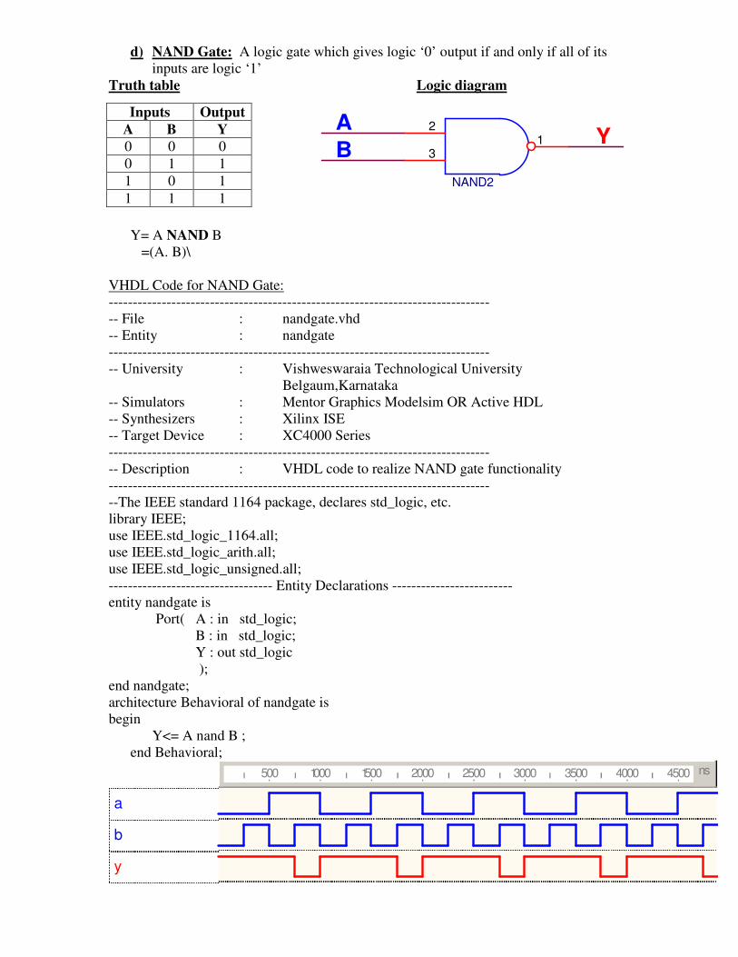
d) NAND Gate: A logic gate which gives logic ‘0’ output if and only if all of its inputs are logic ‘1’
Truth table Logic diagram
Y= A NAND B =(A. B)\
VHDL Code for NAND Gate: ------------------------------------------------------------------------------- -- File : nandgate.vhd -- Entity : nandgate ------------------------------------------------------------------------------- -- University : Vishweswaraia Technological University Belgaum,Karnataka -- Simulators : Mentor Graphics Modelsim OR Active HDL -- Synthesizers : Xilinx ISE -- Target Device : XC4000 Series ------------------------------------------------------------------------------- -- Description : VHDL code to realize NAND gate functionality ------------------------------------------------------------------------------- --The IEEE standard 1164 package, declares std_logic, etc. library IEEE; use IEEE.std_logic_1164.all; use IEEE.std_logic_arith.all; use IEEE.std_logic_unsigned.all; ---------------------------------- Entity Declarations ------------------------- entity nandgate is Port( A : in std_logic; B : in std_logic; Y : out std_logic ); end nandgate; architecture Behavioral of nandgate is begin Y<= A nand B ;
end Behavioral;
Inputs Output A B Y 0 0 0 0 1 1 1 0 1 1 1 1
BNAND2
12
3
AY
a
b
y
ns500 1000 1500 2000 2500 3000 3500 4000 4500
e) NOR Gate: A logic gate whose output logic ‘1’ if and only if all of its inputs are logic ‘0’
Truth table Logic diagram
Y= A NOR B =(A+ B)\
VHDL Code for NOR Gate: ------------------------------------------------------------------------------- -- File : norgate.vhd -- Entity : norgate ------------------------------------------------------------------------------- -- University : Vishweswaraia Technological University Belgaum,Karnataka -- Simulators : Mentor Graphics Modelsim OR Active HDL -- Synthesizers : Xilinx ISE -- Target Device : XC4000 Series ------------------------------------------------------------------------------- -- Description : VHDL code to realize NOR gate functionality ------------------------------------------------------------------------------- --The IEEE standard 1164 package, declares std_logic, etc. library IEEE; use IEEE.std_logic_1164.all; use IEEE.std_logic_arith.all; use IEEE.std_logic_unsigned.all; ---------------------------------- Entity Declarations ------------------------- entity norgate is Port( A : in std_logic; B : in std_logic; Y : out std_logic ); end norgate; architecture Behavioral of norgate is begin Y<= A nor B ;
end Behavioral;
Inputs Output A B Y 0 0 0 0 1 1 1 0 1 1 1 1
YBNOR2
12
3
A
a
b
y
ns2000 2500 3000 3500 4000
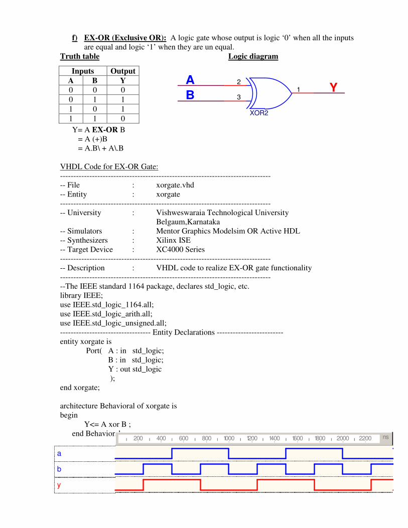
f) EX-OR (Exclusive OR): A logic gate whose output is logic ‘0’ when all the inputs
are equal and logic ‘1’ when they are un equal. Truth table Logic diagram
Y= A EX-OR B = A (+)B = A.B\ + A\.B
VHDL Code for EX-OR Gate: ------------------------------------------------------------------------------- -- File : xorgate.vhd -- Entity : xorgate ------------------------------------------------------------------------------- -- University : Vishweswaraia Technological University Belgaum,Karnataka -- Simulators : Mentor Graphics Modelsim OR Active HDL -- Synthesizers : Xilinx ISE -- Target Device : XC4000 Series ------------------------------------------------------------------------------- -- Description : VHDL code to realize EX-OR gate functionality ------------------------------------------------------------------------------- --The IEEE standard 1164 package, declares std_logic, etc. library IEEE; use IEEE.std_logic_1164.all; use IEEE.std_logic_arith.all; use IEEE.std_logic_unsigned.all; ---------------------------------- Entity Declarations ------------------------- entity xorgate is Port( A : in std_logic; B : in std_logic; Y : out std_logic ); end xorgate; architecture Behavioral of xorgate is begin Y<= A xor B ;
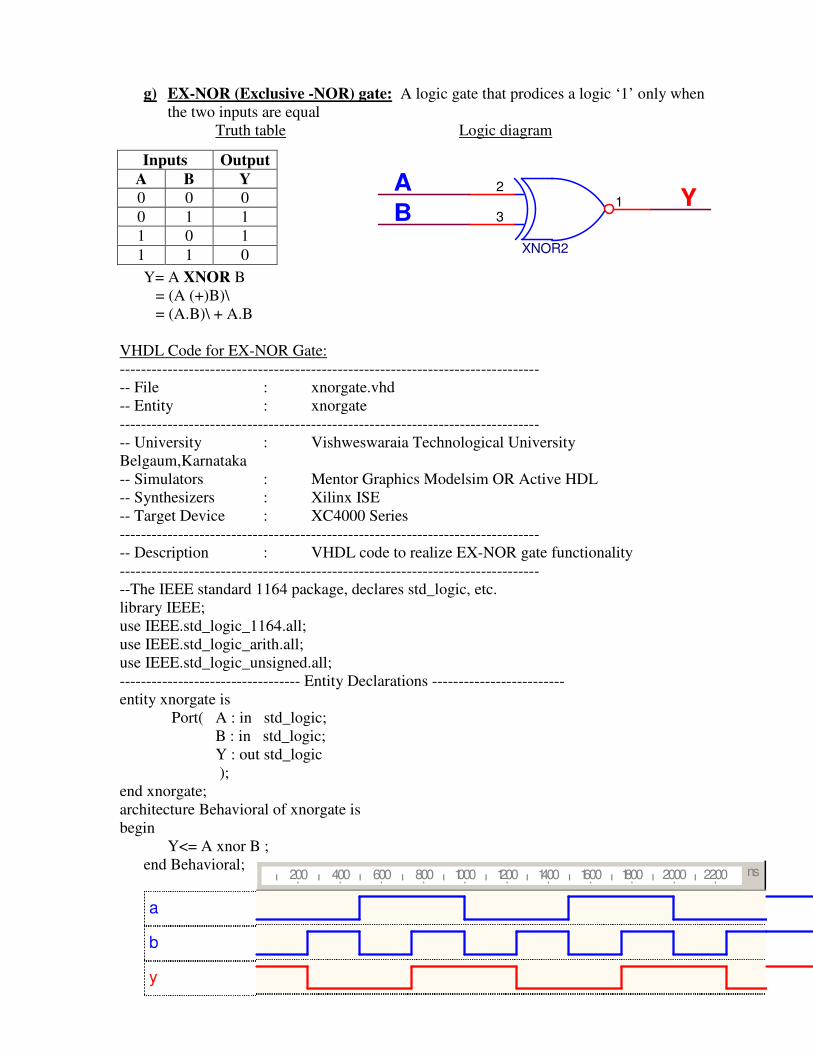
g) EX-NOR (Exclusive -NOR) gate: A logic gate that prodices a logic ‘1’ only when
the two inputs are equal Truth table Logic diagram
Y= A XNOR B = (A (+)B)\ = (A.B)\ + A.B
VHDL Code for EX-NOR Gate: ------------------------------------------------------------------------------- -- File : xnorgate.vhd -- Entity : xnorgate ------------------------------------------------------------------------------- -- University : Vishweswaraia Technological University Belgaum,Karnataka -- Simulators : Mentor Graphics Modelsim OR Active HDL -- Synthesizers : Xilinx ISE -- Target Device : XC4000 Series ------------------------------------------------------------------------------- -- Description : VHDL code to realize EX-NOR gate functionality ------------------------------------------------------------------------------- --The IEEE standard 1164 package, declares std_logic, etc. library IEEE; use IEEE.std_logic_1164.all; use IEEE.std_logic_arith.all; use IEEE.std_logic_unsigned.all; ---------------------------------- Entity Declarations ------------------------- entity xnorgate is Port( A : in std_logic; B : in std_logic; Y : out std_logic ); end xnorgate; architecture Behavioral of xnorgate is begin Y<= A xnor B ;
Experiment 2: Write a VHDL program for the following combinational designs.
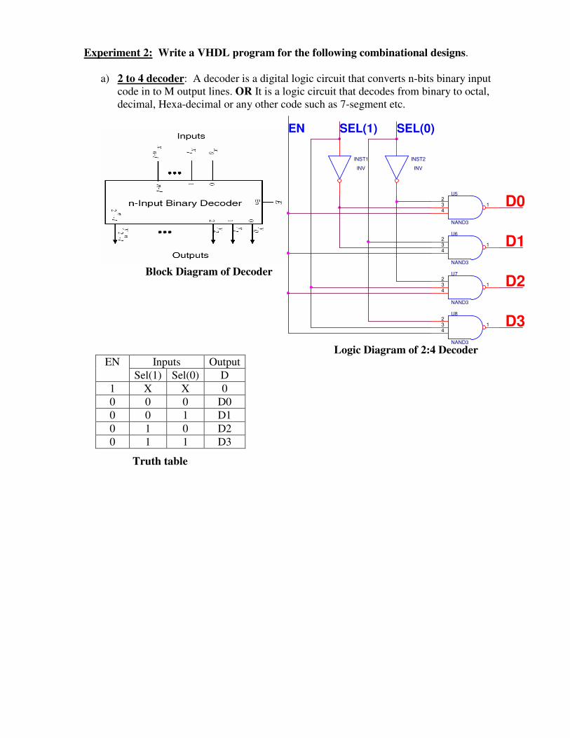
a) 2 to 4 decoder: A decoder is a digital logic circuit that converts n-bits binary input
code in to M output lines. OR It is a logic circuit that decodes from binary to octal, decimal, Hexa-decimal or any other code such as 7-segment etc.
Block Diagram of Decoder
Inputs Output EN Sel(1) Sel(0) D
1 X X 0 0 0 0 D0 0 0 1 D1 0 1 0 D2 0 1 1 D3
Logic Diagram of 2:4 Decoder
Truth table
D3
U6
NAND3
1234
D0
D2
EN
U5
NAND3
1234
SEL(1)
INST1
INV
D1
SEL(0)
INST2
INV
U8
NAND3
1234
U7
NAND3
1234
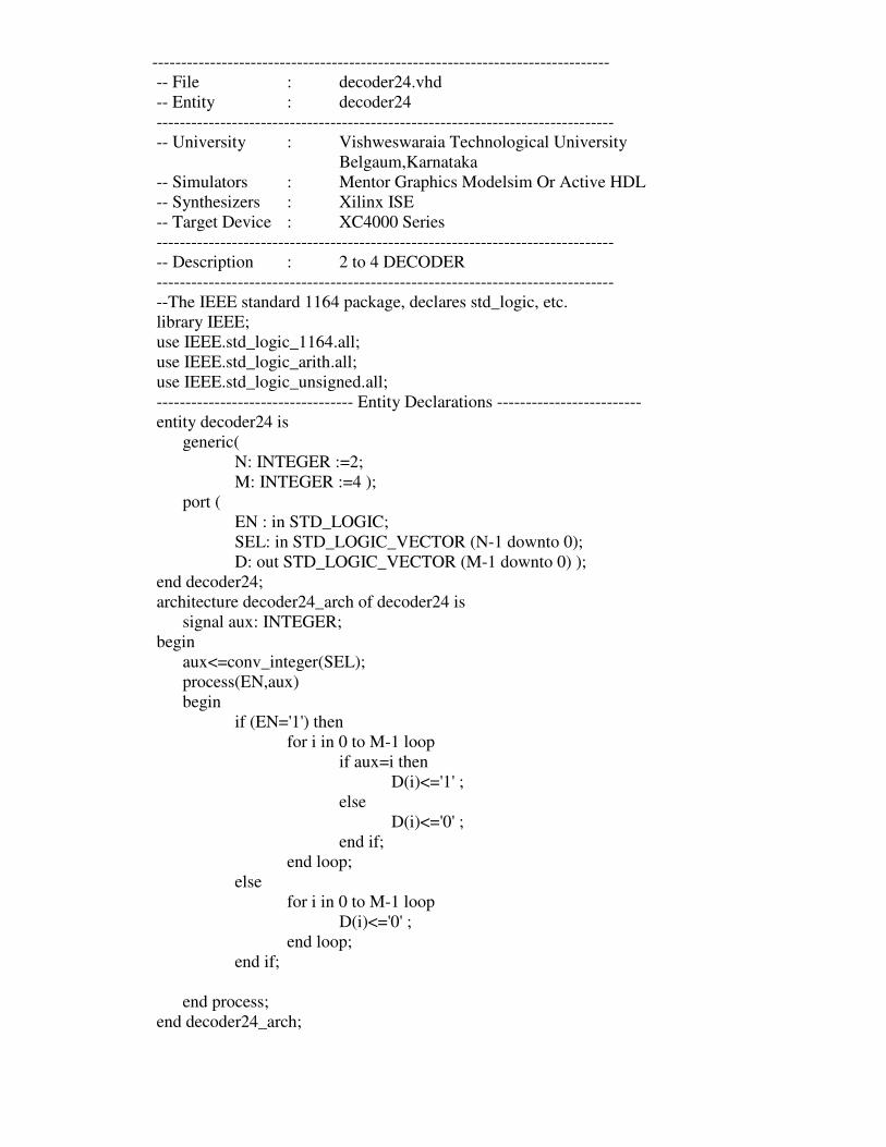
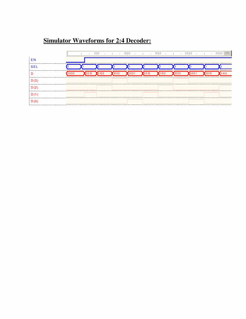
------------------------------------------------------------------------------- -- File : decoder24.vhd -- Entity : decoder24 ------------------------------------------------------------------------------- -- University : Vishweswaraia Technological University Belgaum,Karnataka -- Simulators : Mentor Graphics Modelsim Or Active HDL -- Synthesizers : Xilinx ISE -- Target Device : XC4000 Series ------------------------------------------------------------------------------- -- Description : 2 to 4 DECODER ------------------------------------------------------------------------------- --The IEEE standard 1164 package, declares std_logic, etc. library IEEE; use IEEE.std_logic_1164.all; use IEEE.std_logic_arith.all; use IEEE.std_logic_unsigned.all; ---------------------------------- Entity Declarations ------------------------- entity decoder24 is generic( N: INTEGER :=2; M: INTEGER :=4 ); port ( EN : in STD_LOGIC; SEL: in STD_LOGIC_VECTOR (N-1 downto 0); D: out STD_LOGIC_VECTOR (M-1 downto 0) ); end decoder24; architecture decoder24_arch of decoder24 is signal aux: INTEGER; begin aux<=conv_integer(SEL); process(EN,aux) begin if (EN='1') then for i in 0 to M-1 loop if aux=i then D(i)<='1' ; else D(i)<='0' ; end if; end loop; else for i in 0 to M-1 loop D(i)<='0' ; end loop; end if; end process; end decoder24_arch;
b) 8 to 3 (Encoder without & with priority) Encoder: A logic circuit that produces coded binary outputs from uncoded inputs. Priority encoder: Whenever two or more inputs are applied at a time, internal hardware will check this condition and if the priority is set such that higher numbered input should be taken into account and remaining are considered as don’t care then output code will be appear will be “higher numbered input”. Truth table for 8-input priority encoder EN DIN (7:0) EOUT 0 X X X X X X X X 0 1 X X X X X X X 0 0 1 X X X X X X 0 1 1 1 X X X X X 0 1 1 2 1 X X X X 0 1 1 1 3 1 X X X 0 1 1 1 1 4 1 X X 0 1 1 1 1 1 5 1 X 0 1 1 1 1 1 1 6 1 0 1 1 1 1 1 1 1 7 1 1 1 1 1 1 1 1 1 0
Block Diagram of priority encoder
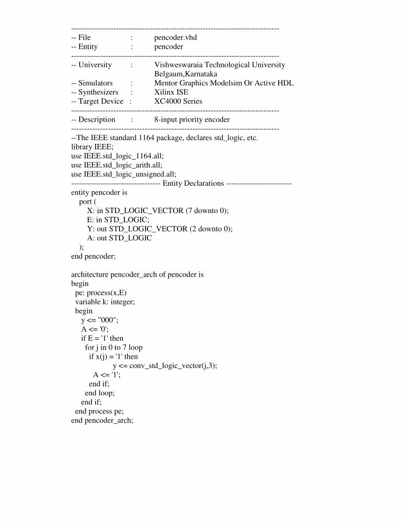
------------------------------------------------------------------------------- -- File : pencoder.vhd -- Entity : pencoder ------------------------------------------------------------------------------- -- University : Vishweswaraia Technological University Belgaum,Karnataka -- Simulators : Mentor Graphics Modelsim Or Active HDL -- Synthesizers : Xilinx ISE -- Target Device : XC4000 Series ------------------------------------------------------------------------------- -- Description : 8-input priority encoder ------------------------------------------------------------------------------- --The IEEE standard 1164 package, declares std_logic, etc. library IEEE; use IEEE.std_logic_1164.all; use IEEE.std_logic_arith.all; use IEEE.std_logic_unsigned.all; ---------------------------------- Entity Declarations ------------------------- entity pencoder is port ( X: in STD_LOGIC_VECTOR (7 downto 0); E: in STD_LOGIC; Y: out STD_LOGIC_VECTOR (2 downto 0); A: out STD_LOGIC ); end pencoder; architecture pencoder_arch of pencoder is begin pe: process(x,E) variable k: integer; begin y <= "000"; A <= '0'; if E = '1' then for j in 0 to 7 loop if x(j) = '1' then y <= conv_std_logic_vector(j,3); A <= '1'; end if; end loop; end if; end process pe; end pencoder_arch;
Simulator Waveforms for 8-input priority encoder:
E
x
x(7)
x(6)
x(5)
x(4)
x(3)
x(2)
x(1)
x(0)
y
y(2)
y(1)
y(0)
A
ns300 400 500 600 700 800 900 1000 1100
05 0A 0F 14 19 1E 23 28 2D
2 3 4
32
5
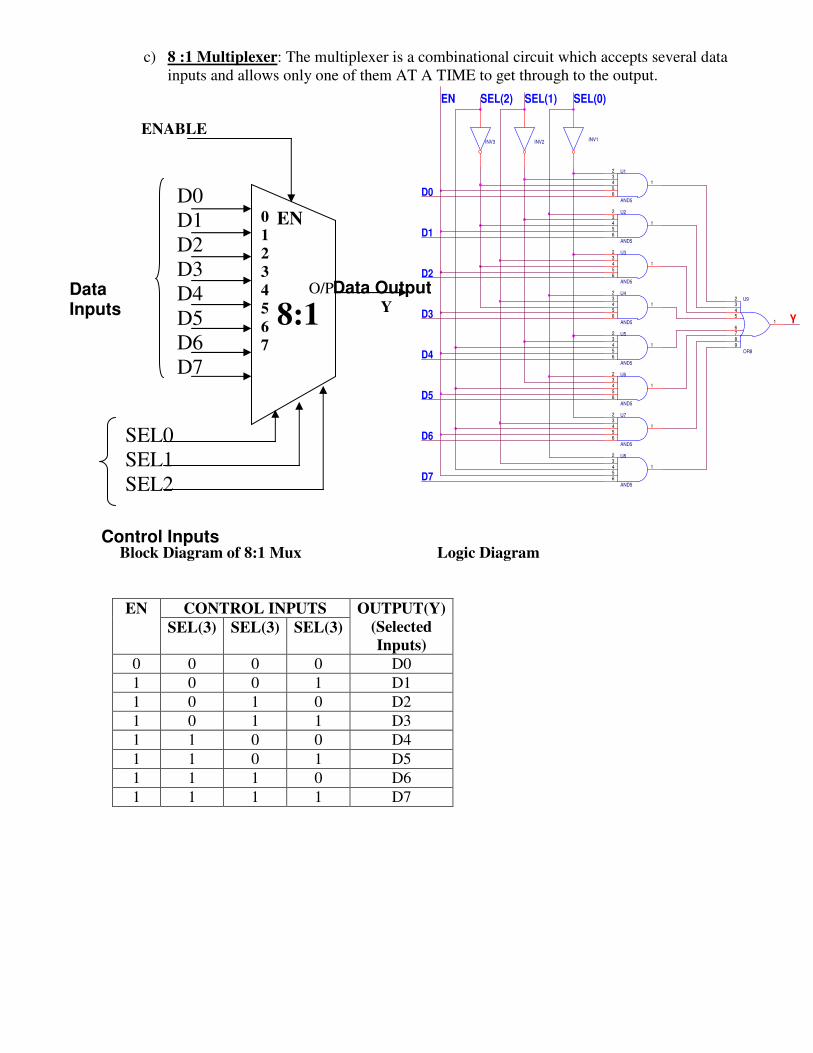
c) 8 :1 Multiplexer: The multiplexer is a combinational circuit which accepts several data inputs and allows only one of them AT A TIME to get through to the output.
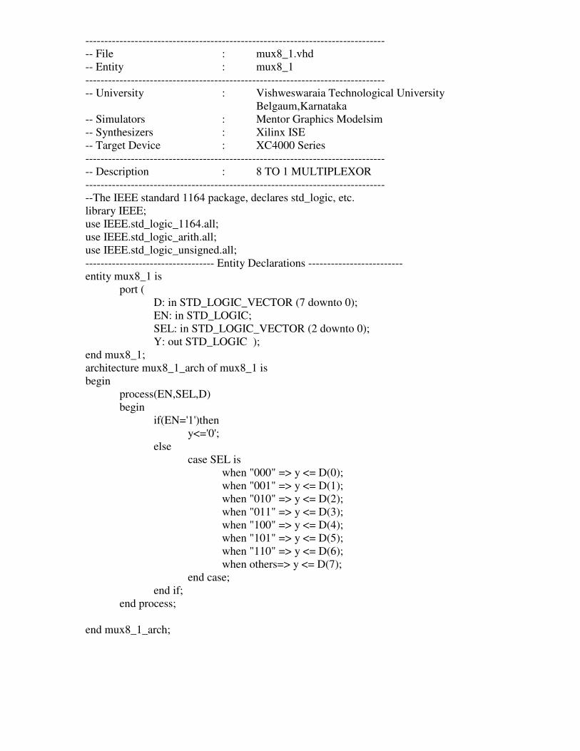
------------------------------------------------------------------------------- -- File : mux8_1.vhd -- Entity : mux8_1 ------------------------------------------------------------------------------- -- University : Vishweswaraia Technological University Belgaum,Karnataka -- Simulators : Mentor Graphics Modelsim -- Synthesizers : Xilinx ISE -- Target Device : XC4000 Series ------------------------------------------------------------------------------- -- Description : 8 TO 1 MULTIPLEXOR ------------------------------------------------------------------------------- --The IEEE standard 1164 package, declares std_logic, etc. library IEEE; use IEEE.std_logic_1164.all; use IEEE.std_logic_arith.all; use IEEE.std_logic_unsigned.all; ---------------------------------- Entity Declarations ------------------------- entity mux8_1 is port ( D: in STD_LOGIC_VECTOR (7 downto 0); EN: in STD_LOGIC; SEL: in STD_LOGIC_VECTOR (2 downto 0); Y: out STD_LOGIC ); end mux8_1; architecture mux8_1_arch of mux8_1 is begin process(EN,SEL,D) begin if(EN='1')then y<='0'; else case SEL is when "000" => y <= D(0); when "001" => y <= D(1); when "010" => y <= D(2); when "011" => y <= D(3); when "100" => y <= D(4); when "101" => y <= D(5); when "110" => y <= D(6); when others=> y <= D(7); end case; end if; end process; end mux8_1_arch;
Simulator Waveforms for 8:1 Multiplexer:
D
D(7)
D(6)
D(5)
D(4)
D(3)
D(2)
D(1)
D(0)
EN
SEL
Y
ns1000 2000 3000 4000 5000 6000 7000 8000 9000
0 1 2 3 4 5 6 7
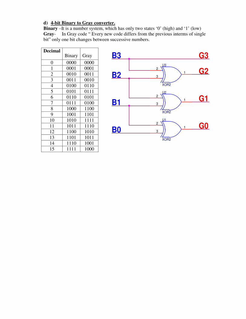
d) 4-bit Binary to Gray converter. Binary –It is a number system, which has only two states ‘0’ (high) and ‘1’ (low) Gray- In Gray code “ Every new code differs from the previous interms of single bit” only one bit changes between successive numbers. Decimal
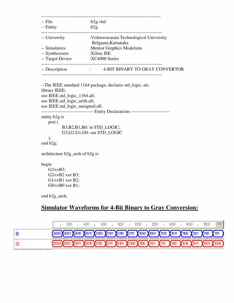
------------------------------------------------------------------------------ -- File :b2g.vhd -- Entity :b2g ------------------------------------------------------------------------------- -- University :Vishweswaraia Technological University Belgaum,Karnataka -- Simulators :Mentor Graphics Modelsim -- Synthesizers :Xilinx ISE -- Target Device :XC4000 Series ------------------------------------------------------------------------------- -- Description : 4-BIT BINARY TO GRAY CONVERTOR ------------------------------------------------------------------------------- --The IEEE standard 1164 package, declares std_logic, etc. library IEEE; use IEEE.std_logic_1164.all; use IEEE.std_logic_arith.all; use IEEE.std_logic_unsigned.all; ---------------------------------- Entity Declarations ------------------------- entity b2g is port ( B3,B2,B1,B0: in STD_LOGIC; G3,G2,G1,G0: out STD_LOGIC ); end b2g; architecture b2g_arch of b2g is begin G3<=B3; G2<=B2 xor B3; G1<=B1 xor B2; G0<=B0 xor B1; end b2g_arch; Simulator Waveforms for 4-Bit Binary to Gray Conversion:
e) Multiplexer, Demultiplexer, comparator. Multiplexer: Ref Exp 2(b) Demultiplexer: Demultiplexer is a combinational circuit that accepts single input and distributes it several outputs (Selectively distributes it to 1 of N output channels) & Exhastly reverse of the multiplexer.
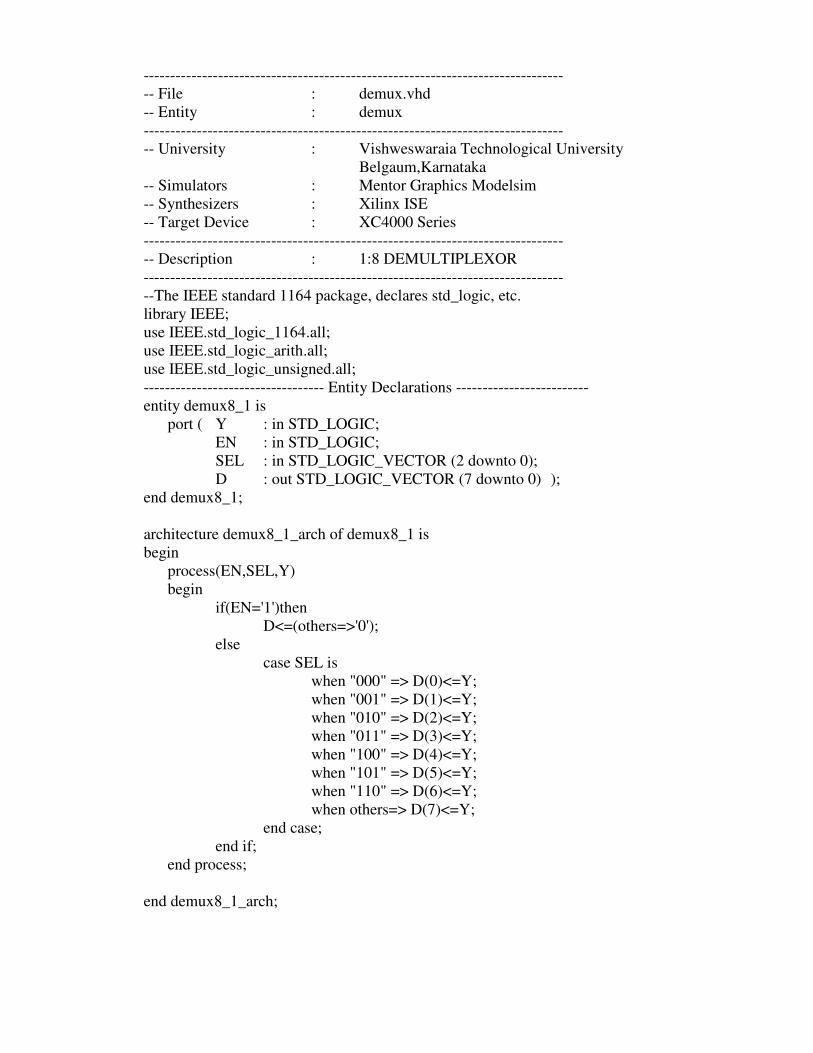
------------------------------------------------------------------------------- -- File : demux.vhd -- Entity : demux ------------------------------------------------------------------------------- -- University : Vishweswaraia Technological University Belgaum,Karnataka -- Simulators : Mentor Graphics Modelsim -- Synthesizers : Xilinx ISE -- Target Device : XC4000 Series ------------------------------------------------------------------------------- -- Description : 1:8 DEMULTIPLEXOR ------------------------------------------------------------------------------- --The IEEE standard 1164 package, declares std_logic, etc. library IEEE; use IEEE.std_logic_1164.all; use IEEE.std_logic_arith.all; use IEEE.std_logic_unsigned.all; ---------------------------------- Entity Declarations ------------------------- entity demux8_1 is port ( Y : in STD_LOGIC; EN : in STD_LOGIC; SEL : in STD_LOGIC_VECTOR (2 downto 0); D : out STD_LOGIC_VECTOR (7 downto 0) ); end demux8_1; architecture demux8_1_arch of demux8_1 is begin process(EN,SEL,Y) begin if(EN='1')then D<=(others=>'0'); else case SEL is when "000" => D(0)<=Y; when "001" => D(1)<=Y; when "010" => D(2)<=Y; when "011" => D(3)<=Y; when "100" => D(4)<=Y; when "101" => D(5)<=Y; when "110" => D(6)<=Y; when others=> D(7)<=Y; end case; end if; end process; end demux8_1_arch;
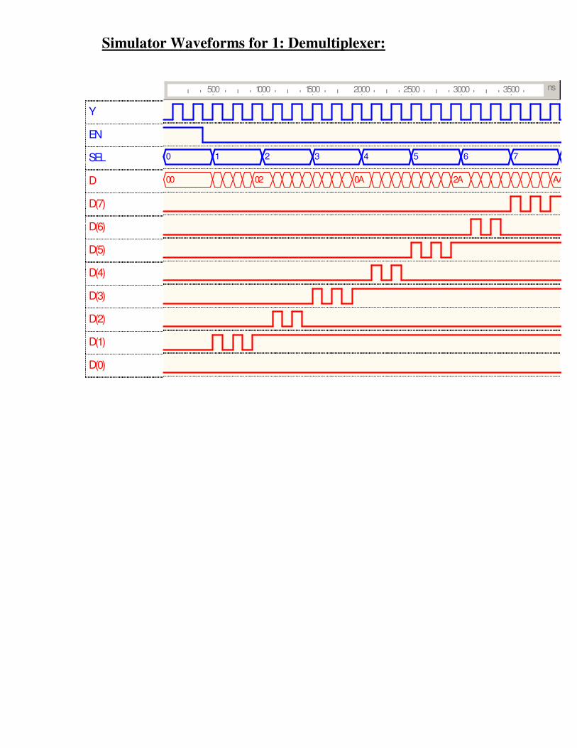
Simulator Waveforms for 1: Demultiplexer:
Y
EN
SEL
D
D(7)
D(6)
D(5)
D(4)
D(3)
D(2)
D(1)
D(0)
ns500 1000 1500 2000 2500 3000 3500
0 1 2 3 4 5 6 7
00 02 0A 2A AA
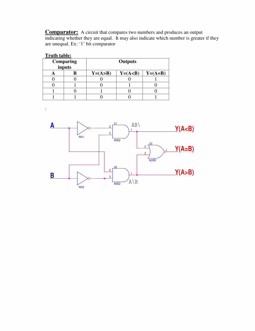
Comparator: A circuit that compares two numbers and produces an output indicating whether they are equal. It may also indicate which number is greater if they are unequal. Ex: ‘1’ bit comparator Truth table:
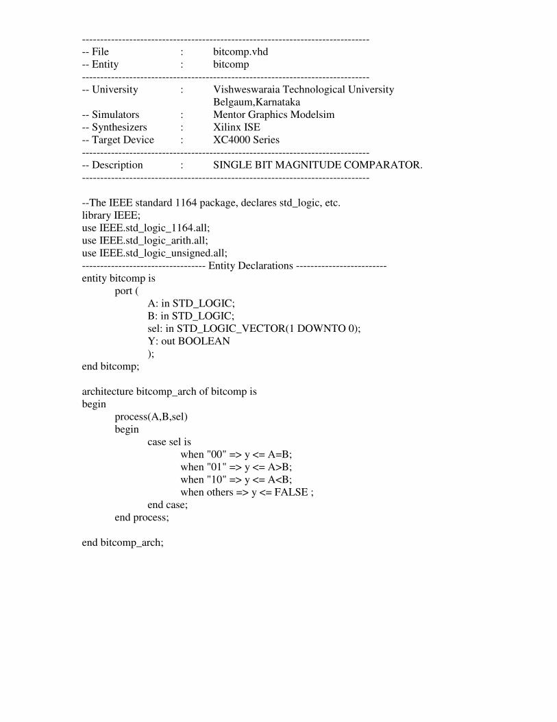
------------------------------------------------------------------------------- -- File : bitcomp.vhd -- Entity : bitcomp ------------------------------------------------------------------------------- -- University : Vishweswaraia Technological University Belgaum,Karnataka -- Simulators : Mentor Graphics Modelsim -- Synthesizers : Xilinx ISE -- Target Device : XC4000 Series ------------------------------------------------------------------------------- -- Description : SINGLE BIT MAGNITUDE COMPARATOR. ------------------------------------------------------------------------------- --The IEEE standard 1164 package, declares std_logic, etc. library IEEE; use IEEE.std_logic_1164.all; use IEEE.std_logic_arith.all; use IEEE.std_logic_unsigned.all; ---------------------------------- Entity Declarations ------------------------- entity bitcomp is port ( A: in STD_LOGIC; B: in STD_LOGIC; sel: in STD_LOGIC_VECTOR(1 DOWNTO 0); Y: out BOOLEAN ); end bitcomp; architecture bitcomp_arch of bitcomp is begin process(A,B,sel) begin case sel is when "00" => y <= A=B; when "01" => y <= A>B; when "10" => y <= A<B; when others => y <= FALSE ; end case; end process; end bitcomp_arch;
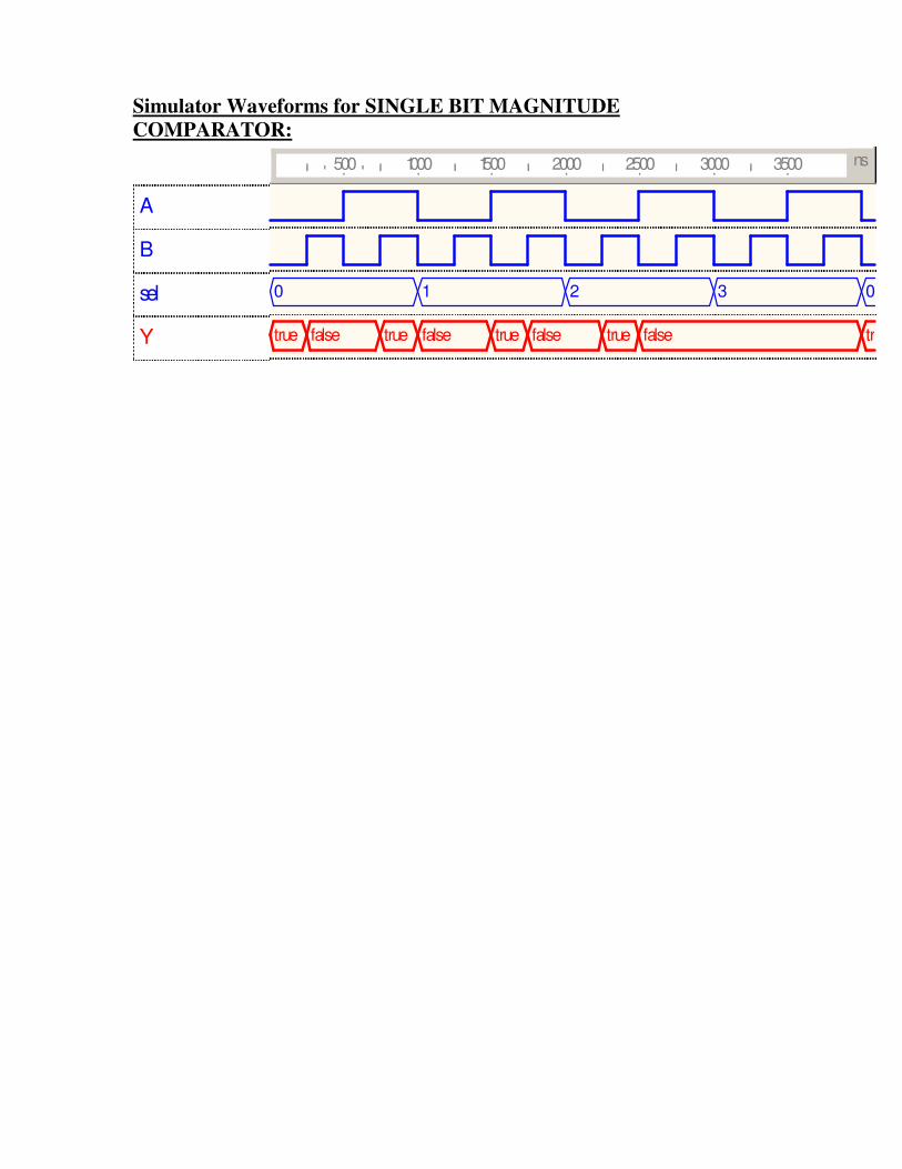
Simulator Waveforms for SINGLE BIT MAGNITUDE COMPARATOR:
A
B
sel
Y
ns500 1000 1500 2000 2500 3000 3500
0 1 2 3
true false true false true false true false
0
true
Experiment 3: Write a VHDL code to describe the functions of full adder using different modeling styles.
A logic circuit for the addition of two one bit numbers is called half adder (sum and carry are output) and a logic circuit that accepts two one-bit signal and Carry-in as inputs and produces their sum and carry as outputs is called full adder. Truth table for Full adder Truth table for Half adder
VHDL Code for HALF ADDER -- File : HA.vhd -- Entity : HA -- Architecture : HA_arch ------------------------------------------------------------------------------- -- University : Vishweswaraia Technological University Belgaum,Karnataka -- Simulators : Mentor Graphics Modelsim -- Synthesizers : Xilinx ISE -- Target Device : XC4000 Series ------------------------------------------------------------------------------- -- Description : HALF ADDER. ------------------------------------------------------------------------------- --The IEEE standard 1164 package, declares std_logic, etc. library IEEE; use IEEE.std_logic_1164.all; use IEEE.std_logic_arith.all; use IEEE.std_logic_unsigned.all; ---------------------------------- Entity Declarations ------------------------- entity HA is port( A,B : in STD_LOGIC; S,CY : out STD_LOGIC ); end HA; architecture HA_arch of HA is begin S<= A XOR B; CY<= A AND B; end HA_arch;
VHDL Code for FULL ADDER -- STRUCTURAL MODELING-A set of interconnect with different COMPONENT -- File : FA.vhd -- Entity : FA -- Architecture : FA_arch ------------------------------------------------------------------------------- -- University : Vishweswaraia Technological University
Belgaum,Karnataka -- Simulators : Mentor Graphics Modelsim -- Synthesizers : Xilinx ISE -- Target Device : XC4000 Series ------------------------------------------------------------------------------- -- Description : FULL ADDER. ------------------------------------------------------------------------------- --The IEEE standard 1164 package, declares std_logic, etc. library IEEE; use IEEE.std_logic_1164.all; use IEEE.std_logic_arith.all; use IEEE.std_logic_unsigned.all; ---------------------------------- Entity Declarations ------------------------- entity FA is port( A,B,Cin : in STD_LOGIC; SUM,CARRY : out STD_LOGIC ); end FA; architecture STRUCTURAL of FA is signal sum1,cy1,cy2:std_logic; component HA port( A,B : in STD_LOGIC; S,CY : out STD_LOGIC ); end component ; begin u1: HA port map(A=>A, B=>B, S=>SUM1, CY=>CY1); u2: HA port map(A=>SUM1, B=>Cin, S=>SUM, CY=>CY2); CARRY<= cy1 OR cy2; end STRUCTURAL;
-- DATAFLOW MODELING-A set of concurrent assignment statements. architecture DATAFLOW of FA is begin SUM<= A XOR B XOR Cin; CARRY<= (A AND B) OR (Cin AND A)OR (Cin AND B); end DATAFLOW; -- BEHAVIORAL MODELING-A set of sequential assignment statements according to -- the behavior of the design. (Process is single concurrent statement, which has sequential statements.) architecture BEHAVIOR of FA is begin process(A,B,Cin) begin SUM<= A XOR B XOR Cin; CARRY<= (A AND B) OR (Cin AND A)OR (Cin AND B); end process; end BEHAVIOR;
Simulator waveforms of HALF ADDER Simulator waveforms of FULL ADDER
A
B
SUM
CARRY
us1 2 3 4 5 6 7 8 9
A
B
Cin
SUM
CARRY
ns100 200 300 400 500 600 700 800 900
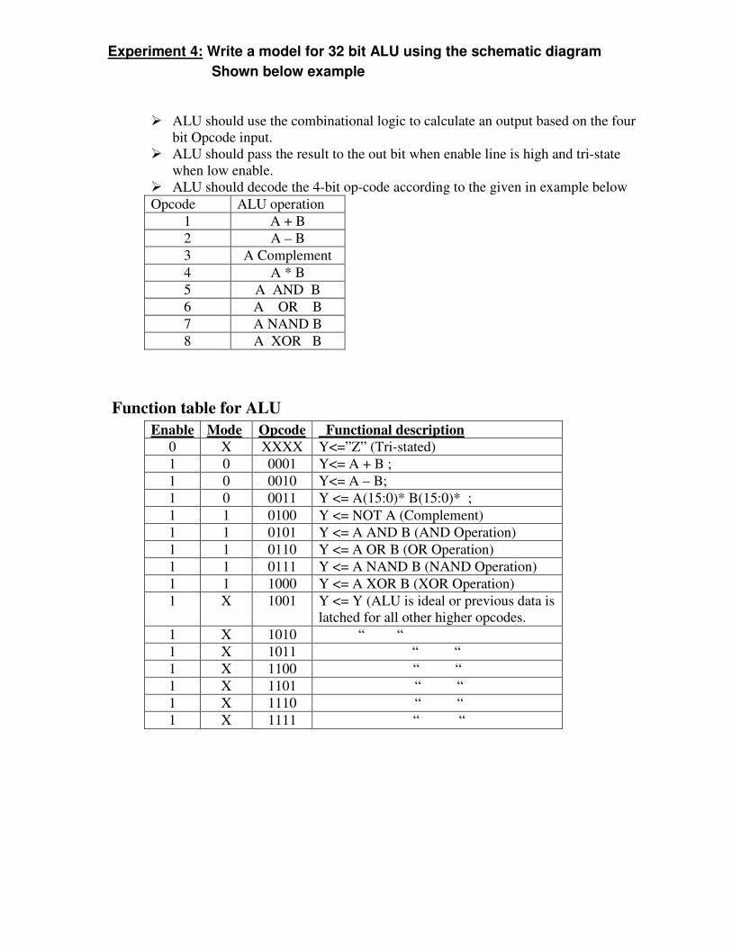
Experiment 4: Write a model for 32 bit ALU using the schematic diagram Shown below example
� ALU should use the combinational logic to calculate an output based on the four bit Opcode input.
� ALU should pass the result to the out bit when enable line is high and tri-state when low enable.
� ALU should decode the 4-bit op-code according to the given in example below Opcode ALU operation
1 A + B 2 A – B 3 A Complement 4 A * B 5 A AND B 6 A OR B 7 A NAND B 8 A XOR B
Function table for ALU Enable Mode Opcode Functional description
0 X XXXX Y<=”Z” (Tri-stated) 1 0 0001 Y<= A + B ; 1 0 0010 Y<= A – B; 1 0 0011 Y <= A(15:0)* B(15:0)* ; 1 1 0100 Y <= NOT A (Complement) 1 1 0101 Y <= A AND B (AND Operation) 1 1 0110 Y <= A OR B (OR Operation) 1 1 0111 Y <= A NAND B (NAND Operation) 1 1 1000 Y <= A XOR B (XOR Operation) 1 X 1001 Y <= Y (ALU is ideal or previous data is
latched for all other higher opcodes. 1 X 10¹⁰ “ “ 1 X 10¹¹ “ “ 1 X 1100 “ “ 1 X 1101 “ “ 1 X 1110 “ “ 1 X 1111 “ “
ARTHAMETIC LOGIC UNIT (ALU) ALU is logic circuit which is able to perform different arithmetic and logical function basically ALU is the heart of central processing unit (CPU).
Opcode [3:0]
Mode Mode : ‘0’____ Arthmatic operation ‘1’____Logic operation Enable ‘0’ Y <= “ Z “ ‘1’ Out put performed Note: For A*B, A&B lower 16 bit [15:0] can be taken in to consideration.
One stage of Arithmetic circuit
One stage of Logic circuit
2:1 Mux
0
1 32
32 4
32 32
Enable
A B
Cin Cin + 1 (CY)
0
1 32 Y
(Data o/p)
Data i/p
Control Signals
VHDL Code for 8_bit ALU: -- File : alu.vhd -- Entity : alu ------------------------------------------------------------------------------- -- University : Vishweswaraia Technological University Belgaum,Karnataka -- Simulators : Mentor Graphics Modelsim -- Synthesizers : Xilinx ISE -- Target Device : XC4000 Series ------------------------------------------------------------------------------- -- Description : 8-bit ALU. ------------------------------------------------------------------------------- --The IEEE standard 1164 package, declares std_logic, etc. library IEEE; use IEEE.Std_Logic_1164.all; use IEEE.NUMERIC_STD.all; ---------------------------------- Entity Declarations ------------------------- -- NOTE : JUST BY CHANGING THE WIDTH OF INPUT AND OUTPUT OF (31 DOWNTO O) -- WILL BECOME 32-BIT ALU -------------------------------------------------------------------------------- entity Alu is port( Clk : in Std_Logic; MODE,EN: in Std_Logic; A,B : in Std_Logic_Vector(7 downto 0); OPCODE : in Std_Logic_Vector(3 downto 0); Y : out Std_Logic_Vector(7 downto 0)); end Alu; architecture Alu_a of Alu is signal C_s : Unsigned(7 downto 0); begin process (A, B,OPCODE,mode) variable A_v : Unsigned(7 downto 0); variable B_v : Unsigned(7 downto 0); begin A_v := Unsigned(A); B_v := Unsigned(B); if(EN='0')then C_s<=(others=>'Z'); if(mode='0')then case OPCODE is when "0000" => C_s <= A_v + B_v; when "0001" => C_s <= A_v - B_v; when "0010" => C_s <= A_v(3 downto 0) * B_v(3 downto 0); when others => C_s <= (others => '0'); end case; else case opcode is when "0011" => C_s <= not A_v;
when "0100" => C_s <= not B_v; when "0101" => C_s <= A_v and B_v; when "0110" => C_s <= A_v nand B_v; when "0111" => C_s <= A_v or B_v; when "1000" => C_s <= A_v nor B_v; when "1001" => C_s <= A_v xor B_v; when "1010" => C_s <= A_v xnor B_v; when others => C_s <= (others => '0'); end case; end if; end if; end process; process begin wait until Clk'event and Clk = '1'; y <= Std_Logic_Vector(C_s); end process ; end Alu_a; Simulator waveforms for 8_bit ALU:
Clk
MODE
EN
A
B
OPCODE
Y
ns50 100 150 200 250 300 350
0 1 2 3 4 3 4 5 6 7 8 9 A B C
UU 04 20 00 F7 FB 00 FF 0C F3 0C F3
08
04
D
00
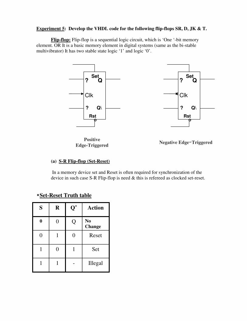
Experiment 5: Develop the VHDL code for the following flip-flops SR, D, JK & T.
Flip-flop: Flip-flop is a sequential logic circuit, which is ‘One ‘-bit memory element. OR It is a basic memory element in digital systems (same as the bi-stable multivibrator) It has two stable state logic ‘1’ and logic ‘0’.
(a) S-R Flip-flop (Set-Reset) In a memory device set and Reset is often required for synchronization of the device in such case S-R Flip-flop is need & this is refereed as clocked set-reset.
�Set-Reset Truth table
? Q Clk ? Q\
o
o
Set
Rst
? Q Clk ? Q\
o
Set
Rst
Positive Edge-Triggered Negative Edge-Triggered
Illegal - 1 1
Set 1 0 1
Reset 0 1 0
No Change
Q 0 0
Action Q+ R S
VHDL Code for SR Flip-Flop: ------------------------------------------------------------------------------- -- File : SRFF.vhd -- Entity : SRFF ------------------------------------------------------------------------------- -- University : Vishweswaraia Technological University Belgaum,Karnataka -- Simulators : Mentor Graphics Modelsim Or Active HDL -- Synthesizers : Xilinx ISE -- Target Device : XC4000 Series ------------------------------------------------------------------------------- -- Description : SR Flip-Flop ------------------------------------------------------------------------------- --The IEEE standard 1164 package, declares std_logic, etc. library IEEE; use IEEE.std_logic_1164.all; use IEEE.std_logic_arith.all; use IEEE.std_logic_unsigned.all; ---------------------------------- Entity Declarations ------------------------- entity SRFF is port ( CLK, RST, S, R : in std_logic; Q, Qn : out std_logic); end SRFF; architecture RTL of SRFF is signal FF : std_logic; begin process (CLK, RST) variable SR : std_logic_vector(1 downto 0); begin if (RST = '0') then FF <= '0'; elsif (CLK'event and CLK = '1') then SR := S & R; case SR is when "01" => FF <= '0'; when "10" => FF <= '1'; when "11" => FF <= 'Z'; when others => FF <= FF; end case; end if; end process; Q <= FF ; Qn <= not FF ; end RTL;
Simulator waveforms for SR Flip-Flop:
CLK
RST
S
R
Q
Qn
ns200 400 600 800 1000 1200 1400
(b) D- FF (Delay Flip-flop)
In D-Flip-flop the transfer of data from the input to the Output is delayed and hence the name delay D-Flip-flop. The D-Type Flip-flop is either used as a delay device or as a latch to store ‘1’ bit of binary information. D input transferred to Q output when clock asserted
D-F/F Truth table
Note: - D is used to avoid the possibility of race condition in SR flip flop.
- The Output = Input when clock is applied.
Set 1 1
Reset 0 0
Action Q+ D
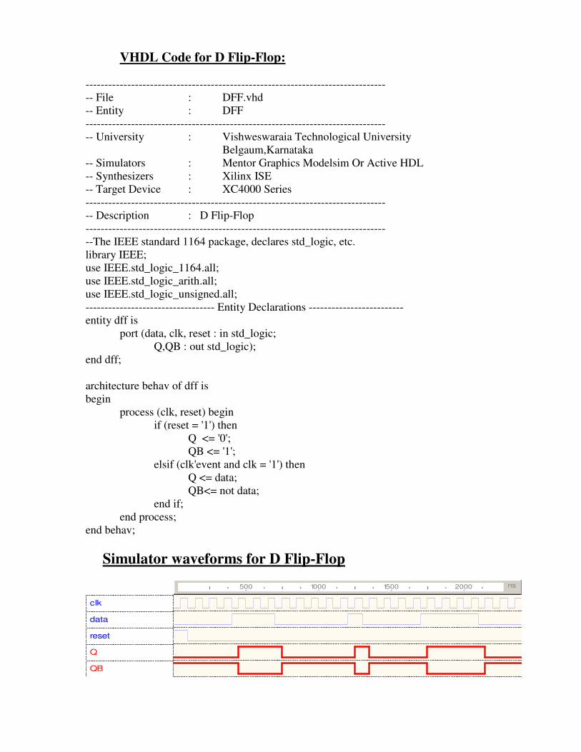
VHDL Code for D Flip-Flop:
------------------------------------------------------------------------------- -- File : DFF.vhd -- Entity : DFF ------------------------------------------------------------------------------- -- University : Vishweswaraia Technological University Belgaum,Karnataka -- Simulators : Mentor Graphics Modelsim Or Active HDL -- Synthesizers : Xilinx ISE -- Target Device : XC4000 Series ------------------------------------------------------------------------------- -- Description : D Flip-Flop ------------------------------------------------------------------------------- --The IEEE standard 1164 package, declares std_logic, etc. library IEEE; use IEEE.std_logic_1164.all; use IEEE.std_logic_arith.all; use IEEE.std_logic_unsigned.all; ---------------------------------- Entity Declarations ------------------------- entity dff is port (data, clk, reset : in std_logic; Q,QB : out std_logic); end dff; architecture behav of dff is begin process (clk, reset) begin if (reset = '1') then Q <= '0'; QB <= '1'; elsif (clk'event and clk = '1') then Q <= data; QB<= not data; end if; end process; end behav;
Simulator waveforms for D Flip-Flop
clk
data
reset
Q
QB
ns500 1000 1500 2000
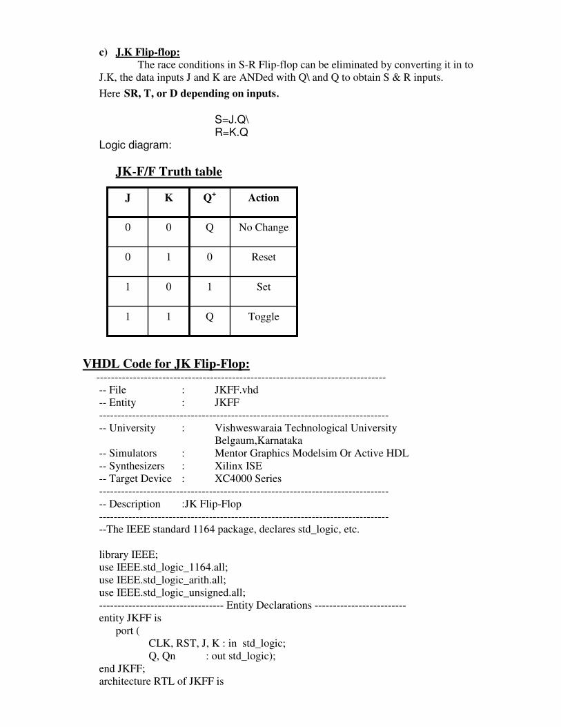
c) J.K Flip-flop: The race conditions in S-R Flip-flop can be eliminated by converting it in to J.K, the data inputs J and K are ANDed with Q\ and Q to obtain S & R inputs. Here SR, T, or D depending on inputs. S=J.Q\ R=K.Q Logic diagram:
JK-F/F Truth table
VHDL Code for JK Flip-Flop: -------------------------------------------------------------------------------
-- File : JKFF.vhd -- Entity : JKFF ------------------------------------------------------------------------------- -- University : Vishweswaraia Technological University Belgaum,Karnataka -- Simulators : Mentor Graphics Modelsim Or Active HDL -- Synthesizers : Xilinx ISE -- Target Device : XC4000 Series ------------------------------------------------------------------------------- -- Description :JK Flip-Flop ------------------------------------------------------------------------------- --The IEEE standard 1164 package, declares std_logic, etc. library IEEE; use IEEE.std_logic_1164.all; use IEEE.std_logic_arith.all; use IEEE.std_logic_unsigned.all; ---------------------------------- Entity Declarations ------------------------- entity JKFF is port ( CLK, RST, J, K : in std_logic; Q, Qn : out std_logic); end JKFF; architecture RTL of JKFF is
Toggle Q 1 1
Set 1 0 1
Reset 0 1 0
No Change Q 0 0
Action Q+ K J
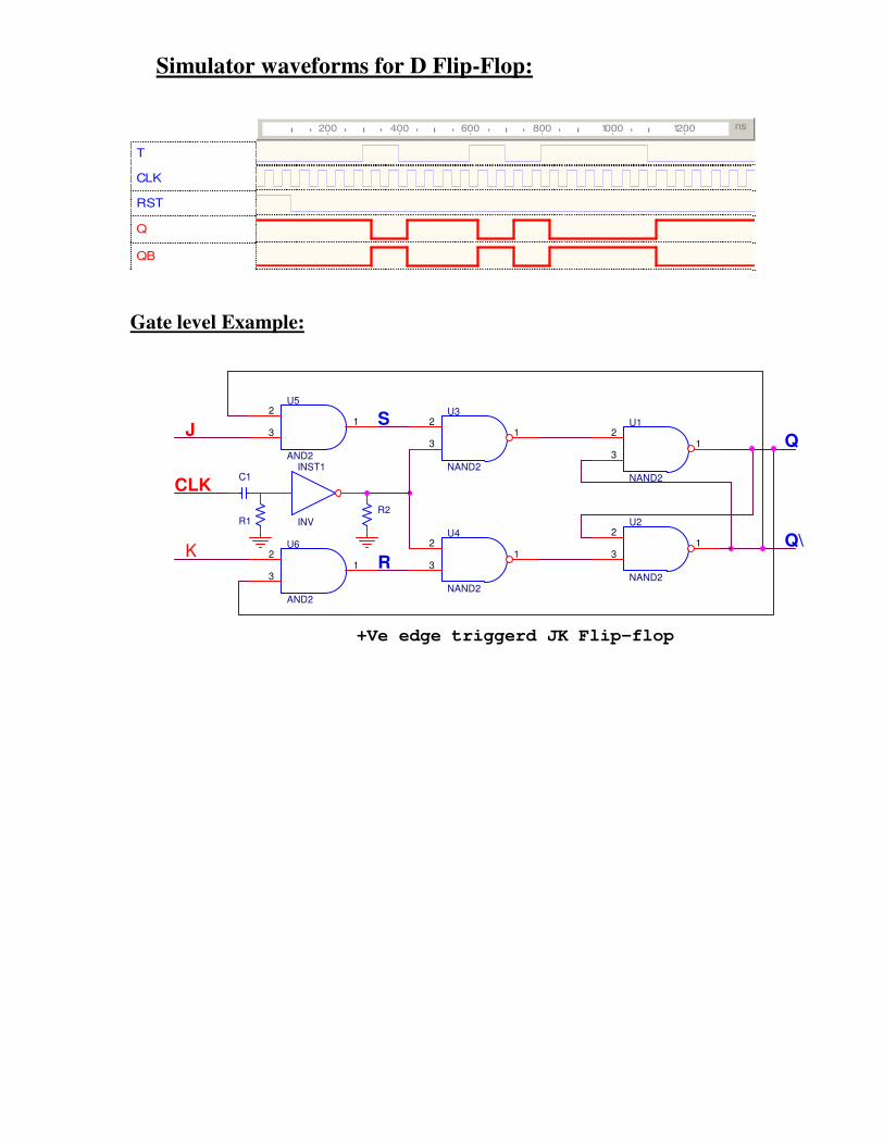
signal FF : std_logic; begin process (CLK, RST) variable JK : std_logic_vector(1 downto 0); begin if (RST = '0') then FF <= '0'; elsif (CLK'event and CLK = '1') then JK := J & K; case JK is when "01" => FF <= '0'; when "10" => FF <= '1'; when "11" => FF <= not FF; when others => FF <= FF; end case; end if; end process; Q <= FF ; Qn <= not FF ; end RTL; Simulator waveforms for JK Flip-Flop
CLK
RSTn
J
K
Q
Qn
ns600 700 800 900 1000 1100 1200 1300 1400
d) T-Flip-flop (Toggle Flip-flop): On every change in clock pulse the output ‘Q’ changes its state (Toggle). A Flip-flop with one data input which changes state for every clock pulse.(J=K=’1’ in JQK Flip-flop the resulting output is ‘T’ Flip-flop).
T-F/F Truth table VHDL Code for T Flip-Flop: ------------------------------------------------------------------------------ -- File : TFF.vhd -- Entity : TFF ------------------------------------------------------------------------------- -- University : Vishweswaraia Technological University Belgaum,Karnataka -- Simulators : Mentor Graphics Modelsim Or Active HDL -- Synthesizers : Xilinx ISE -- Target Device : XC4000 Series ------------------------------------------------------------------------------- -- Description : T Flip-Flop ------------------------------------------------------------------------------- --The IEEE standard 1164 package, declares std_logic, etc. library IEEE; use IEEE.std_logic_1164.all; use IEEE.std_logic_arith.all; use IEEE.std_logic_unsigned.all; ---------------------------------- Entity Declarations ------------------------- entity tff is port (T, CLK, RST : in std_logic; Q,QB : out std_logic); end tff; architecture behav of tff is begin process (clk, RST) begin if (RST = '1') then Q <= '1'; QB <= '0'; elsif (clk'event and clk = '1') then QB <= T; Q <= not T; end if; end process; end behav;
Toggle Q 1
No Change Q 0
Action Q+
T
Simulator waveforms for D Flip-Flop:
T
CLK
RST
Q
QB
ns200 400 600 800 1000 1200
Gate level Example:
U3
NAND2
12
3 Q
U6
AND2
12
3
U2
NAND2
12
3
C1CLK
U4
NAND2
12
3
R2R1
J
Q\
+Ve edge triggerd JK Flip-flop
R
INST1
INV
U1
NAND2
12
3
S
K
U5
AND2
12
3
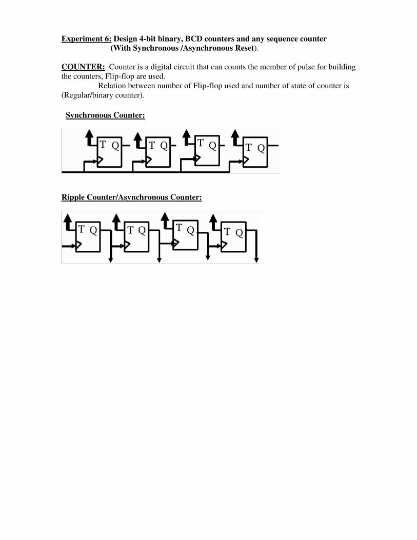
Experiment 6: Design 4-bit binary, BCD counters and any sequence counter
(With Synchronous /Asynchronous Reset). COUNTER: Counter is a digital circuit that can counts the member of pulse for building the counters, Flip-flop are used. Relation between number of Flip-flop used and number of state of counter is (Regular/binary counter).
Ripple Counter/Asynchronous Counter:
Synchronous Counter:
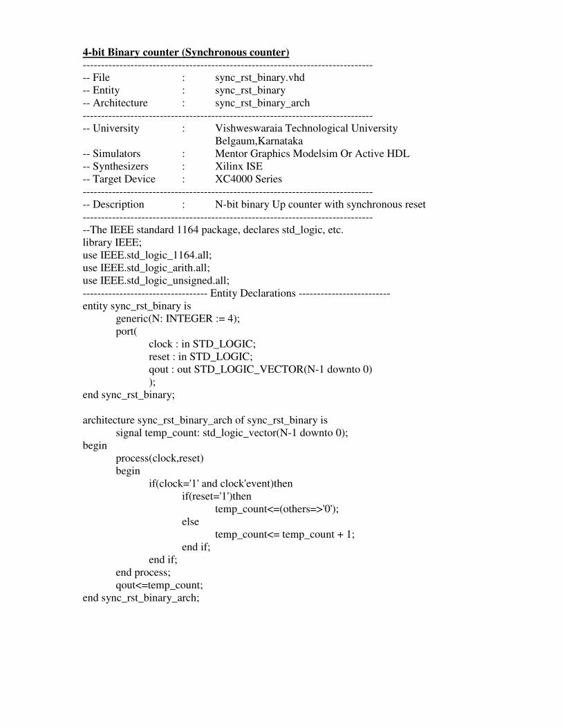
4-bit Binary counter (Synchronous counter) ------------------------------------------------------------------------------- -- File : sync_rst_binary.vhd -- Entity : sync_rst_binary -- Architecture : sync_rst_binary_arch ------------------------------------------------------------------------------- -- University : Vishweswaraia Technological University Belgaum,Karnataka -- Simulators : Mentor Graphics Modelsim Or Active HDL -- Synthesizers : Xilinx ISE -- Target Device : XC4000 Series ------------------------------------------------------------------------------- -- Description : N-bit binary Up counter with synchronous reset ------------------------------------------------------------------------------- --The IEEE standard 1164 package, declares std_logic, etc. library IEEE; use IEEE.std_logic_1164.all; use IEEE.std_logic_arith.all; use IEEE.std_logic_unsigned.all; ---------------------------------- Entity Declarations ------------------------- entity sync_rst_binary is generic(N: INTEGER := 4); port( clock : in STD_LOGIC; reset : in STD_LOGIC; qout : out STD_LOGIC_VECTOR(N-1 downto 0) ); end sync_rst_binary; architecture sync_rst_binary_arch of sync_rst_binary is signal temp_count: std_logic_vector(N-1 downto 0); begin process(clock,reset) begin if(clock='1' and clock'event)then if(reset='1')then temp_count<=(others=>'0'); else temp_count<= temp_count + 1; end if; end if; end process; qout<=temp_count; end sync_rst_binary_arch;
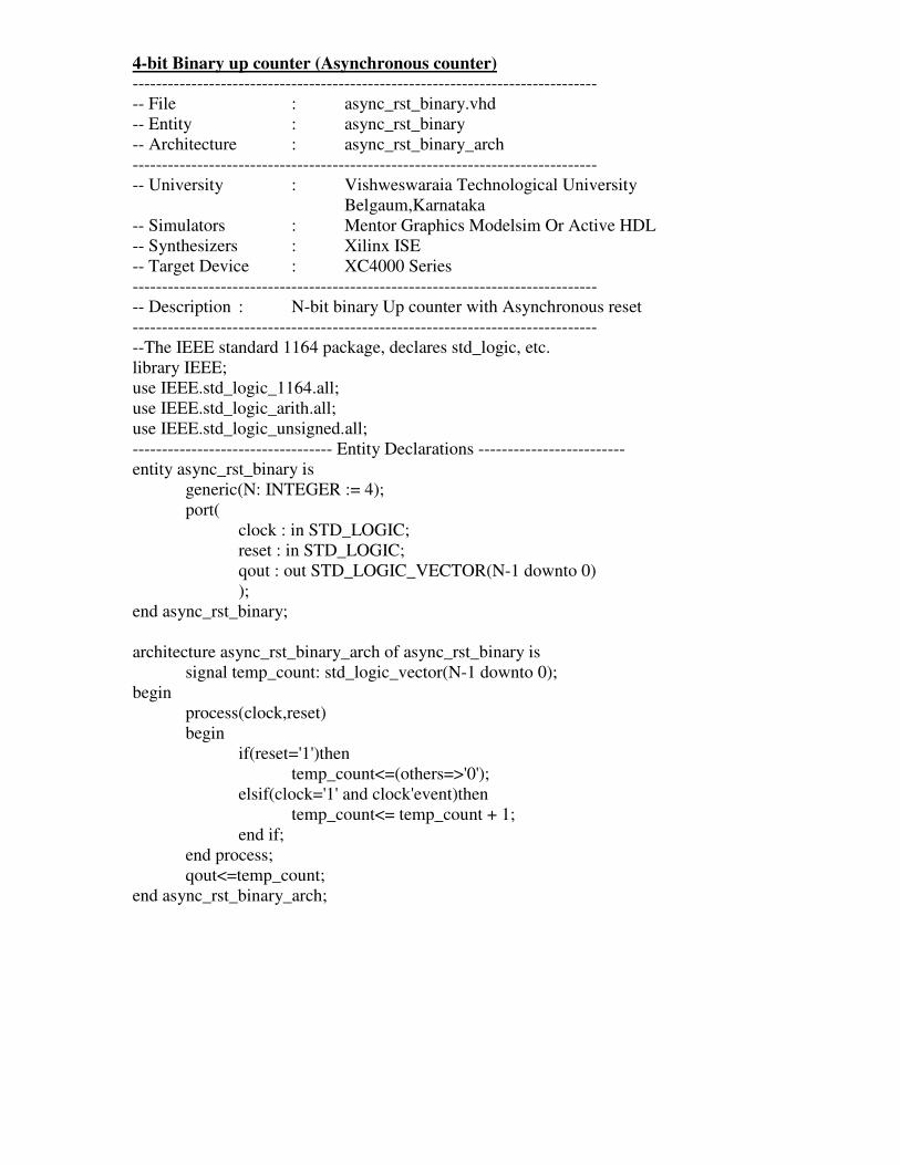
4-bit Binary up counter (Asynchronous counter) ------------------------------------------------------------------------------- -- File : async_rst_binary.vhd -- Entity : async_rst_binary -- Architecture : async_rst_binary_arch ------------------------------------------------------------------------------- -- University : Vishweswaraia Technological University Belgaum,Karnataka -- Simulators : Mentor Graphics Modelsim Or Active HDL -- Synthesizers : Xilinx ISE -- Target Device : XC4000 Series ------------------------------------------------------------------------------- -- Description : N-bit binary Up counter with Asynchronous reset ------------------------------------------------------------------------------- --The IEEE standard 1164 package, declares std_logic, etc. library IEEE; use IEEE.std_logic_1164.all; use IEEE.std_logic_arith.all; use IEEE.std_logic_unsigned.all; ---------------------------------- Entity Declarations ------------------------- entity async_rst_binary is generic(N: INTEGER := 4); port( clock : in STD_LOGIC; reset : in STD_LOGIC; qout : out STD_LOGIC_VECTOR(N-1 downto 0) ); end async_rst_binary; architecture async_rst_binary_arch of async_rst_binary is signal temp_count: std_logic_vector(N-1 downto 0); begin process(clock,reset) begin if(reset='1')then temp_count<=(others=>'0'); elsif(clock='1' and clock'event)then temp_count<= temp_count + 1; end if; end process; qout<=temp_count; end async_rst_binary_arch;
4-bit BCD up counter (Synchronous counter) ------------------------------------------------------------------------------- -- File : sync_rst_BCD.vhd -- Entity : sync_rst_BCD -- Architecture : sync_rst_BCD_arch ------------------------------------------------------------------------------- -- University : Vishweswaraia Technological University
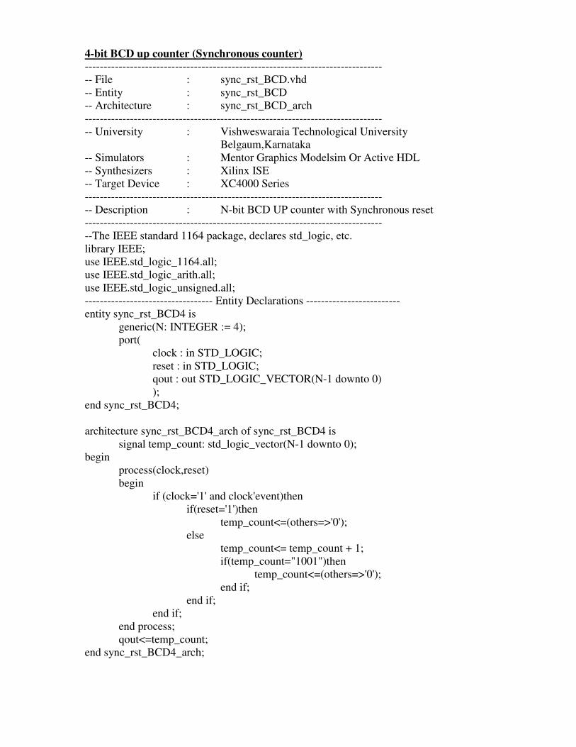
Belgaum,Karnataka -- Simulators : Mentor Graphics Modelsim Or Active HDL -- Synthesizers : Xilinx ISE -- Target Device : XC4000 Series ------------------------------------------------------------------------------- -- Description : N-bit BCD UP counter with Synchronous reset ------------------------------------------------------------------------------- --The IEEE standard 1164 package, declares std_logic, etc. library IEEE; use IEEE.std_logic_1164.all; use IEEE.std_logic_arith.all; use IEEE.std_logic_unsigned.all; ---------------------------------- Entity Declarations ------------------------- entity sync_rst_BCD4 is generic(N: INTEGER := 4); port( clock : in STD_LOGIC; reset : in STD_LOGIC; qout : out STD_LOGIC_VECTOR(N-1 downto 0) ); end sync_rst_BCD4; architecture sync_rst_BCD4_arch of sync_rst_BCD4 is signal temp_count: std_logic_vector(N-1 downto 0); begin process(clock,reset) begin if (clock='1' and clock'event)then if(reset='1')then temp_count<=(others=>'0'); else temp_count<= temp_count + 1; if(temp_count="1001")then temp_count<=(others=>'0'); end if; end if; end if; end process; qout<=temp_count; end sync_rst_BCD4_arch;
4-bit BCD up counter (Asynchronous Reset) ------------------------------------------------------------------------------- -- File : async_rst_BCD.vhd -- Entity : async_rst_BCD -- Architecture : async_rst_BCD_arch ------------------------------------------------------------------------------- -- University : Vishweswaraia Technological University
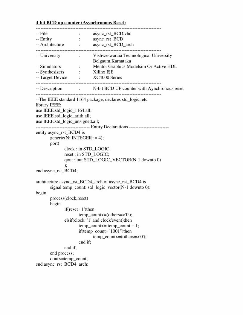
Belgaum,Karnataka -- Simulators : Mentor Graphics Modelsim Or Active HDL -- Synthesizers : Xilinx ISE -- Target Device : XC4000 Series ------------------------------------------------------------------------------- -- Description : N-bit BCD UP counter with Aynchronous reset ------------------------------------------------------------------------------- --The IEEE standard 1164 package, declares std_logic, etc. library IEEE; use IEEE.std_logic_1164.all; use IEEE.std_logic_arith.all; use IEEE.std_logic_unsigned.all; ---------------------------------- Entity Declarations ------------------------- entity async_rst_BCD4 is generic(N: INTEGER := 4); port( clock : in STD_LOGIC; reset : in STD_LOGIC; qout : out STD_LOGIC_VECTOR(N-1 downto 0) ); end async_rst_BCD4; architecture async_rst_BCD4_arch of async_rst_BCD4 is signal temp_count: std_logic_vector(N-1 downto 0); begin process(clock,reset) begin if(reset='1')then temp_count<=(others=>'0'); elsif(clock='1' and clock'event)then temp_count<= temp_count + 1; if(temp_count="1001")then temp_count<=(others=>'0'); end if; end if; end process; qout<=temp_count; end async_rst_BCD4_arch;
4-bit Gray up counter (Asynchronous Reset) ------------------------------------------------------------------------------- -- File : graycnt.vhd -- Entity : graycnt -- Architecture : graycnt_arch ------------------------------------------------------------------------------- -- University : Vishweswaraia Technological University
Belgaum,Karnataka -- Simulators : Mentor Graphics Modelsim Or Active HDL -- Synthesizers : Xilinx ISE -- Target Device : XC4000 Series ------------------------------------------------------------------------------- -- Description : N-bit Gary up counter with Asynchronous reset ------------------------------------------------------------------------------- --The IEEE standard 1164 package, declares std_logic, etc. library IEEE; use IEEE.std_logic_1164.all; use IEEE.std_logic_arith.all; use IEEE.std_logic_unsigned.all; ---------------------------------- Entity Declarations ------------------------- entity graycnt is generic(N: INTEGER := 4); port( clock : in STD_LOGIC; reset : in STD_LOGIC; grayout,binaryout : out std_logic_vector(N-1 downto 0) ); end graycnt; architecture graycnt of graycnt is signal temp_count: std_logic_vector(N-1 downto 0); begin process(clock,reset) begin if(reset='1')then temp_count<=(others=>'0'); elsif(clock='1' and clock'event)then temp_count<= temp_count + 1; end if; end process; binaryout<=temp_count; grayout(3)<=temp_count(3); grayout(2)<=temp_count(3)xor temp_count(2); grayout(1)<=temp_count(2)xor temp_count(1); grayout(0)<=temp_count(1)xor temp_count(0); end graycnt;
Waveforms for 4-Bit Binary Up Counter Waveforms for 4-Bit BCD Up Counter
Experiment 7: Write VHDL code to display messages on the given seven-segment display interface.
7-Segment display can display the digits 0-9 and the hex extension (A-F). A signal-character displays bring out leads for 7-segments & the common elect code (Common cathode & common anode).Here in FPGA/CPLD board to interface one 7-segment LED display whose elements are connected to any I/O pins of the FPGA/CPLD. Here we can consider common-anode 7-segment LED displays. The user can then ON by driving associated signal low.
(a) LED segments (b) Four displays with common anode and (c) LED connection on CPLD or FPGA Board. Turning on an LED: (For +5V) Note: If your Seven-segment LED is having Digit point, Then turn on with giving Logic ‘1’ to dig.pt permanently when particular Seven-segment is enabled.
+5V R LED
GAL output pin
+5V R LED
GAL output pin
1
0
+5V
+0.2V +1.7V
No current
Current light
no light
R = voltage current =
5 - 1.7 15 x 10 -3
= 220 ohms
Common Anode
+3.3V/
+3.3V/
VHDL Code for 7-Segment Displays: ---------------------------------------------------------------------------------- -- File : seg7dec.vhd -- Entity : seg7dec ------------------------------------------------------------------------------- -- University : Vishweswaraia Technological University -- Belgaum,Karnataka -- Simulators : Mentor Graphics Modelsim Or Active HDL -- Synthesizers : Xilinx ISE -- Target Device : XC4000 Series ------------------------------------------------------------------------------- -- Description : 7-Segment Decoder ------------------------------------------------------------------------------- --The IEEE standard 1164 package, declares std_logic, etc. library IEEE; use IEEE.std_logic_1164.all; use IEEE.std_logic_arith.all; use IEEE.std_logic_unsigned.all; ---------------------------------- Entity Declarations ------------------------- entity seg7dec is port ( Q : in STD_LOGIC_VECTOR(3 downto 0); AtoG : out STD_LOGIC_VECTOR(6 downto 0)
); end seg7dec; architecture seg7dec_arch of seg7dec is begin process(Q) begin case Q is when "0000" => AtoG <= "0000001"; when "0001" => AtoG <= "1001111"; when "0010" => AtoG <= "0010010"; when "0011" => AtoG <= "0000110"; when "0100" => AtoG <= "1001100"; when "0101" => AtoG <= "0100100"; when "0110" => AtoG <= "0100000"; when "0111" => AtoG <= "0001101"; when "1000" => AtoG <= "0000000"; when "1001" => AtoG <= "0000100"; when "1010" => AtoG <= "0001000"; when "1011" => AtoG <= "1100000"; when "1100" => AtoG <= "0110001"; when "1101" => AtoG <= "1000010"; when "1110" => AtoG <= "0110000"; when others => AtoG <= "0111000"; end case; end process; end seg7dec_arch;
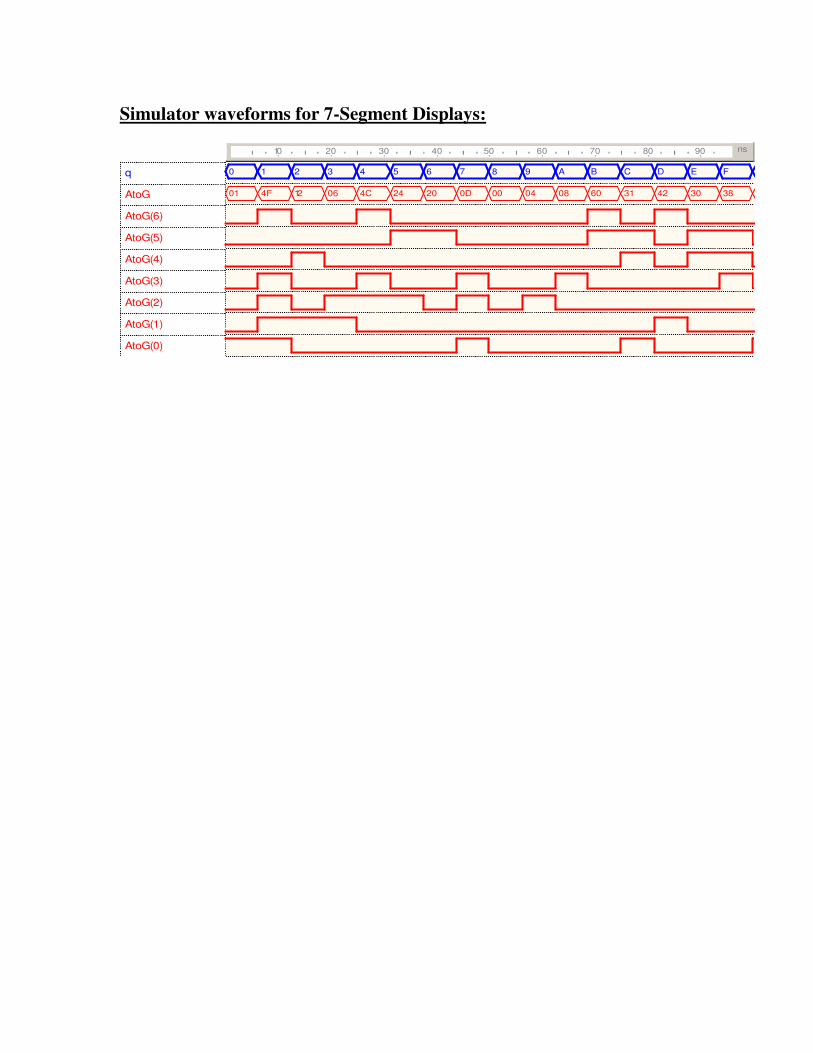
Simulator waveforms for 7-Segment Displays:
q
AtoG
AtoG(6)
AtoG(5)
AtoG(4)
AtoG(3)
AtoG(2)
AtoG(1)
AtoG(0)
ns10 20 30 40 50 60 70 80 90
0 1 2 3 4 5 6 7 8 9 A B C D E F
01 4F 12 06 4C 24 20 0D 00 04 08 60 31 42 30 38
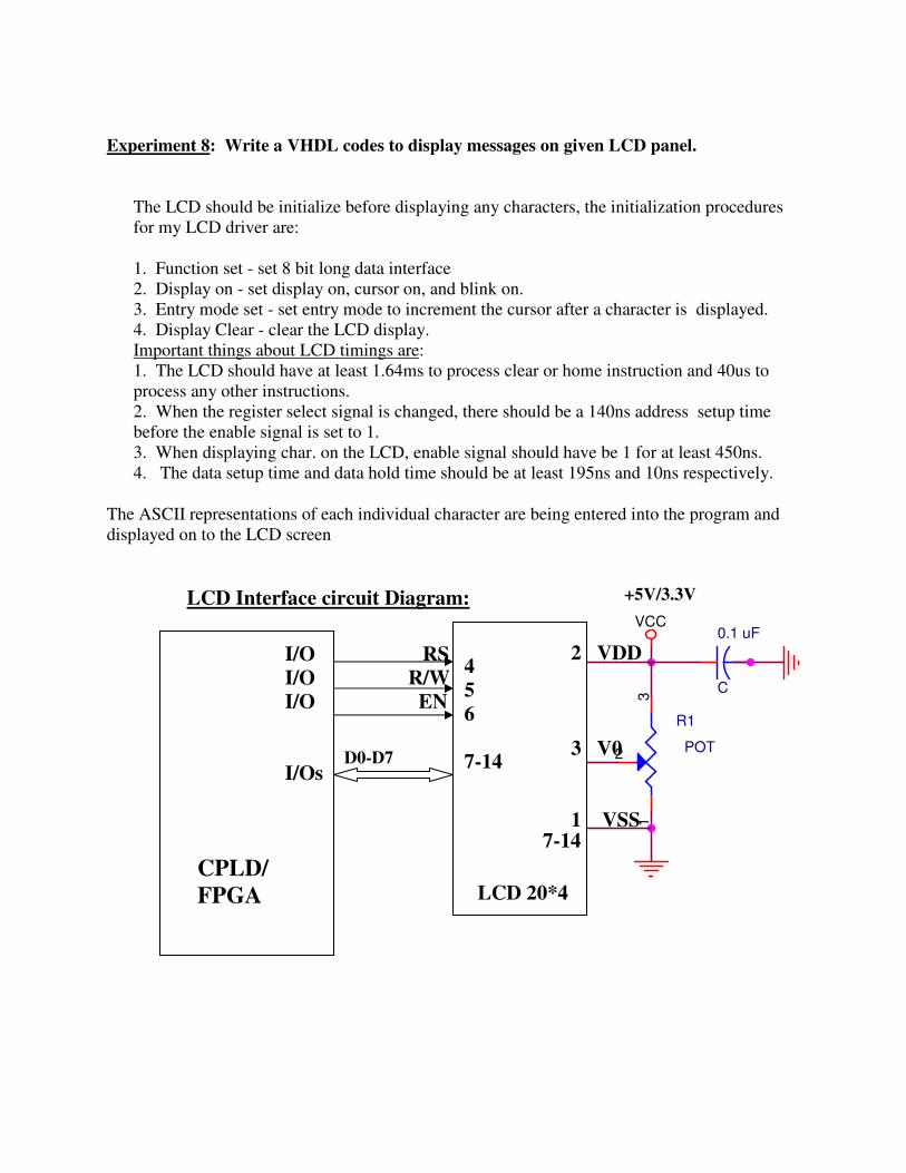
Experiment 8: Write a VHDL codes to display messages on given LCD panel.
The LCD should be initialize before displaying any characters, the initialization procedures for my LCD driver are:
1. Function set - set 8 bit long data interface 2. Display on - set display on, cursor on, and blink on. 3. Entry mode set - set entry mode to increment the cursor after a character is displayed. 4. Display Clear - clear the LCD display. Important things about LCD timings are: 1. The LCD should have at least 1.64ms to process clear or home instruction and 40us to process any other instructions. 2. When the register select signal is changed, there should be a 140ns address setup time before the enable signal is set to 1. 3. When displaying char. on the LCD, enable signal should have be 1 for at least 450ns. 4. The data setup time and data hold time should be at least 195ns and 10ns respectively.
The ASCII representations of each individual character are being entered into the program and displayed on to the LCD screen
LCD Interface circuit Diagram:
R1
POT
13
2
VCC0.1 uF
C
CPLD/FPGA
7-14
D0-D7
I/O RS I/O R/W I/O EN I/Os
4 5 6 7-14
2 VDD 3 V0 1 VSS
LCD 20*4
+5V/3.3V
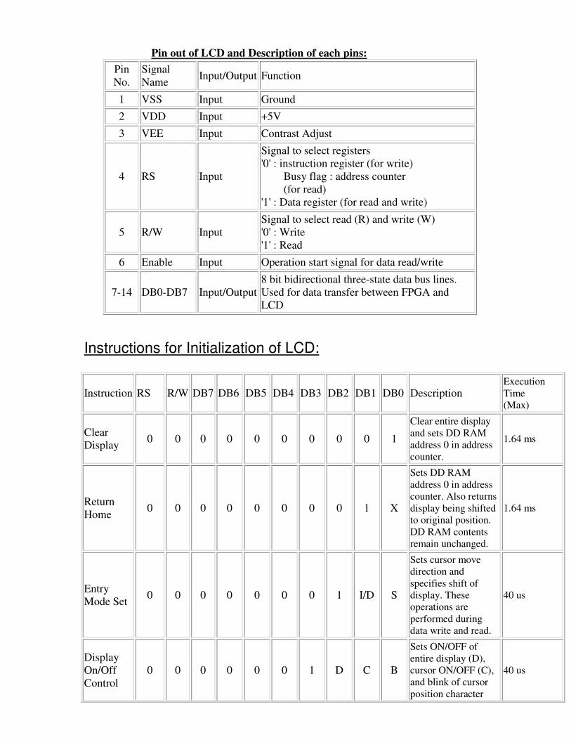
Pin out of LCD and Description of each pins:
Pin No.
Signal Name Input/Output Function
1 VSS Input Ground
2 VDD Input +5V
3 VEE Input Contrast Adjust
4 RS Input
Signal to select registers '0' : instruction register (for write) Busy flag : address counter (for read) '1' : Data register (for read and write)
5 R/W InputSignal to select read (R) and write (W) '0' : Write '1' : Read
6 Enable Input Operation start signal for data read/write
7-14 DB0-DB7 Input/Output8 bit bidirectional three-state data bus lines. Used for data transfer between FPGA and LCD
Clear entire display and sets DD RAM address 0 in address counter.
1.64 ms
Return Home 0 0 0 0 0 0 0 0 1 X
Sets DD RAM address 0 in address counter. Also returns display being shifted to original position. DD RAM contents remain unchanged.
1.64 ms
Entry Mode Set 0 0 0 0 0 0 0 1 I/D S
Sets cursor move direction and specifies shift of display. These operations are performed during data write and read.
40 us
Display On/Off Control
0 0 0 0 0 0 1 D C B
Sets ON/OFF of entire display (D), cursor ON/OFF (C), and blink of cursor position character
40 us
(B).
Cursor or Display Shift
0 0 0 0 0 1 S/C R/L X X
Moves cursor and shifts display without changing DD RAM contents
40 us
Function Set 0 0 0 0 1 DL N F X X
Sets interface data length (DL), number of display lines (L) and character font (F).
40 us
Set CG RAM Address
0 0 0 1 ACG
Sets CG RAM address. CG RAM data is sent and received after this setting.
40 us
Set DD RAM Address
0 0 1 ADD
Sets DD RAM address. DD RAM data is sent and received after this setting
40 us
Read Busy Flag & Address
0 1 BF AC
Reads Busy flag (BF) indicating internal operation is being performed and reads address counter contents.
0 us
Write Data to CG or DD RAM
1 0 Write Data Writes data into DD RAM or CG RAM 40 us
Read Data from CG or DD RAM
1 1 Read Data Reads data from DD RAM or CG RAM 40 us
I/D = 1 : Increment I/D = 0 : Decrement S = 1 : Accompanies display shift S/C = 1 : Display shift S/C = 0 : Cursor move R/L = 1 : Shift to the right R/L = 0 : Shift to the left DL = 1 : 8 bits, DL = 0 : 4 bits N = 1 : 2 lines, N = 0 : 1 lines F = 1 : 5*10 dots, F = 0 : 5*7 dots BF = 1 : Internally operating BF = 0 : Can accept instruction X : Don't Care
DD RAM : Display data RAM CG RAM : Character generator RAM ACG : CG RAM address ADD : DD RAM address : Corresponds to cursor address AC : Address counter used for both DD and CG RAM address
Notes:
• After power on, the LCD has to wait more than 15 ms for Vcc rises to 4.5V before accepting the first instruction.
• I set signal "count" count from 0 to 3. However, this value is depend on the system clock. Make sure the LCD has enough time to execute the next instruction. Execution time for each instruction(Follow the instruction table).
• VHDL example for LCD display Initialization
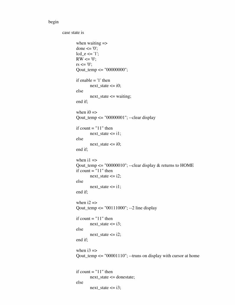
--------------------------------------------------------------------------------------------------- -- File : lcd_init.vhd -- Entity : lcd_init --------------------------------------------------------------------------------------------------- -- University : Vishweswaraia Technological University Belgaum,Karnataka -- Simulators : Mentor Graphics Modelsim -- Synthesizers : Xilinx ISE -- Target Device : XC4000 Series ------------------------------------------------------------------------------------------------ -- Description : This program initialize the LCD display ----------------------------------------------------------------------------------------------- --The IEEE standard 1164 package, declares std_logic, etc. library IEEE; use IEEE.Std_Logic_1164.all; use IEEE.Std_Logic_unsigned.all; use IEEE.NUMERIC_STD.all; ---------------------------------- Entity Declarations ------------------------- entity lcd_init is generic(width : positive := 8); port(reset, clock, enable, done_ack : in std_logic; done, RW, rs, lcd_e : out std_logic; Qout : buffer std_logic_vector(width-1 downto 0) ); end lcd_init; architecture initial of lcd_init is type state_type is (waiting, i0, i1, i2, i3, donestate); signal state, next_state : state_type; signal count,count_temp : std_logic_vector(1 downto 0); signal Qout_temp : std_logic_vector(width-1 downto 0); begin running : process(state,enable,done_ack,count) is
begin case state is when waiting => done <= '0'; lcd_e <= '1'; RW <= '0'; rs <= '0'; Qout_temp <= "00000000"; if enable = '1' then next_state <= i0; else next_state <= waiting; end if; when i0 => Qout_temp <= "00000001"; --clear display if count = "11" then next_state <= i1; else next_state <= i0; end if; when i1 => Qout_temp <= "00000010"; --clear display & returns to HOME if count = "11" then next_state <= i2; else next_state <= i1; end if; when i2 => Qout_temp <= "00111000"; --2 line display if count = "11" then next_state <= i3; else next_state <= i2; end if; when i3 => Qout_temp <= "00001110"; --truns on display with cursor at home if count = "11" then next_state <= donestate; else next_state <= i3;
end if; when donestate => done <= '1'; Qout_temp <= ( others => '0' ); if done_ack = '1' then next_state <= waiting; else next_state <= donestate; end if; end case; end process running; timing : process(clock,reset) is begin if rising_edge(clock) then Qout <= Qout_temp; count <= count_temp; if reset = '1' then state <= waiting; count_temp <= "00"; else state <= next_state; count_temp <= count_temp + "01"; end if; end if; end process timing; end initial;
• Simulator waveforms for LCD display Initialization:
clock
reset
enable
done_ack
done
RW
rs
lcd_e
Qout
state
next_state
count
count_temp
Qout_temp
ns200 400 600 800 1000 1200 1400 1600
00 01 02 38 0E
waiting i0 i1 i2 i3
waiting i1 i2 i3
U 0 1 2 3 0 1 2 3 0 1 2 3 0 1 2 3 0 1
0 1 2 3 0 1 2 3 0 1 2 3 0 1 2 3 0 1 2
00 01 02 38 0E
00
donestate
donestate
00
Experiment 9: Write codes to operate the given stepper motor. Stepper motors are electromechanical devices Which converts a digital pulses in mechanical rotation, that provide accurate incremental rotation.
The most common stepper motor uses four windings for a four-phase operation. A typical four-phase motor driving circuit is shown in Figure using an FPGA to generate the sequence logic. The clock (CLK) input synchronizes the logic and determines the speed of rotation. The motor advances one step per clock period; the angle of rotation of the shaft will depend on the particular motor.To determine the clock period, consider that the stepper motor torque increases as frequency decreases. The direction (DIR) control input changes the sequence at the outputs (PH1 to PH4) to reverse the motor direction. The enable input (EN) determines whether the motor is rotating or holding. The active low reset input (RST) initializes the circuit to ensure that the correct starting sequence is provided to the outputs.. The enhanced sequence provides increased torque but requires twice the current.
Note: Please go through the datasheet or Voltage and Current ratings of stepper motor and Decide The transistor selection depends on drive current, power dissipation, and gain.(Preferably NPN Power Darlington transistors). The series resistors should be selected to limit the FPGA current to 8 mA per output, 1/4 Watt resistors Value. Typical Ratings available stepper motor are:
1. The four windings have a common connection to the motor supply voltage (VS), typically ranges from 5 to 30 Volts.
2. Each motor phase current may range from 100 mA to as much as 10 A.
CPLD/FPGA
Stepper motor sequencing: There are several kinds of sequences that can be used to drive stepper motors. The following tables give the most common sequences for energizing the coils. Following the steps in ascending order drives the motor in one direction, going in descending order drives the motor the other way. This sequence interleaves the normal and wave sequences.
If step angle = 1.8, For One revolution 360/1.8=200 steps(In Full step mode)
If step angle = 0.9, For One revolution 360/0.9=400 steps(In Half step mode) Bipolar stepper motor will not run in Half step mode for any consult the stepper motor manufacturer.
Make this sequence in Descending order motor rotates in opposite direction(This sequence will be provided by the stepper motor manufacturer).
VHDL Code Uni-polar Stepper Motor Controller in Full step mode: ------------------------------------------------------------------------------------ -- File : SMControl.vhd -- Entity : SMControl ------------------------------------------------------------------------------------ -- University : Vishweswaraia Technological University Belgaum,Karnataka -- Simulators : Mentor Graphics Modelsim -- Synthesizers : Xilinx ISE -- Target Device : XC4000 Series ---------------------------------------------------------------------------------------- -- Description : Uni-polar Stepper Motor Controller in Full step ----- mode ---------------------------------------------------------------------------------------- --The IEEE standard 1164 package, declares std_logic, etc. library IEEE; use IEEE.Std_Logic_1164.all; use IEEE.NUMERIC_STD.all; ---------------------------------- Entity Declarations ------------------------- ---- -- NOTE : Ask the stepping sequence from stepper motor manufacturer -- and change your VHDL code this sequence commonly used ------------------------------------------------------------------------------------------ entity SMControl is Port (Clk,Reset,E,Dir: in std_logic; Sec : out std_logic_vector(3 downto 0) ); end SMControl; architecture Behavioral of SMControl is Type States is (Step_0, Step_1, Step_2, Step_3); Signal Next_State, Current_State : States; begin Process( Clk, Reset, Current_State ) Begin if Reset = '1' then Next_State <= Step_0; elsif Clk'event and Clk = '1' then Case Current_State is When Step_0 => Sec <= x"A"; if E = '1' then Next_State <= Step_0; else If DIR = '1' then Next_State <= Step_1; Else Next_State <= Step_3; End if; end if; When Step_1 => Sec <= x"9"; if E = '1' then
Next_State <= Step_1; else If DIR = '1' then Next_State <= Step_2; Else Next_State <= Step_0; End if; end if; When Step_2 => Sec <= x"5"; if E = '1' then Next_State <= Step_2; else If DIR = '1' then Next_State <= Step_3; Else Next_State <= Step_1; End if; end if; When Step_3 => Sec <= x"6"; if E = '1' then Next_State <= Step_3; else If DIR = '1' then Next_State <= Step_0; Else Next_State <= Step_2; End if; end if; When Others => Next_State <= Step_0; end Case; end if; end Process; Process(Clk) Begin if Clk'event and clk = '1' then Current_State <= Next_State; end if; end process; end Behavioral;
State machine Diagram according to step changes:
Simulator waveforms for Uni-polar Stepper Motor Controller in Full step mode: