Page 1
HAL Id: hal-02980827https://hal.archives-ouvertes.fr/hal-02980827
Submitted on 27 Oct 2020
HAL is a multi-disciplinary open accessarchive for the deposit and dissemination of sci-entific research documents, whether they are pub-lished or not. The documents may come fromteaching and research institutions in France orabroad, or from public or private research centers.
L’archive ouverte pluridisciplinaire HAL, estdestinée au dépôt et à la diffusion de documentsscientifiques de niveau recherche, publiés ou non,émanant des établissements d’enseignement et derecherche français ou étrangers, des laboratoirespublics ou privés.
‘ig,vgs’ Monitoring for Fast and Robust SiC MOSFETShort-Circuit Protection with High integration
CapabilityYazan Barazi, François Boige, Nicolas Rouger, Jean-Marc Blaquiere, Frédéric
Richardeau
To cite this version:Yazan Barazi, François Boige, Nicolas Rouger, Jean-Marc Blaquiere, Frédéric Richardeau. ‘ig,vgs’Monitoring for Fast and Robust SiC MOSFET Short-Circuit Protection with High integration Capabil-ity. 2020 22nd European Conference on Power Electronics and Applications (EPE’20 ECCE Europe),Sep 2020, Lyon (Virtual ), France. pp.P.1-P.10, 10.23919/EPE20ECCEEurope43536.2020.9215619.hal-02980827
Page 2
1
‘ig,vgs’ Monitoring for Fast and Robust SiC MOSFET Short-Circuit
Protection with High integration Capability
Yazan Barazi, François Boige, Nicolas Rouger, Jean-Marc Blaquiere, Frédéric Richardeau
LAPLACE, University of Toulouse, CNRS, INPT, UPS, Toulouse, France
2 rue Charles Camichel Toulouse P722 - 31071
Toulouse, France
Tel.: +33 / (0)5 – 3432.23.91.
Fax: +33 / (x)5 – 6163.88.75.
[email protected] ; [email protected] ; [email protected] ;
[email protected] ; [email protected] ;
http://www.laplace.univ-tlse.fr/
Acknowledgements
This research work has been supported financially by the French Ministry in higher education,
research and innovation.
Keywords
«Silicon Carbide (SiC)», «signal processing», «Robust control», «intelligent drive», «Protection
device»
Abstract
SiC MOSFETs have a low short circuit withstand time. To address this challenge, a soft shut down
and two original detection methods are proposed in this paper, easily implemented and based-on (ig,
vgs) diagnosis with no direct time dependency. The first one is dedicated for SiC MOSFETs using his
gate-leakage thermal runaway current, and the second one is more general and faster using the gate-
charge monitoring. Both are experimentally validated and compared in terms of response-time and
robustness capability.
Introduction
The Silicon Carbide (SiC) MOSFETs offers several advantages, low switching losses, higher
switching frequencies and high temperature stability [1]. However, today, the short-circuit (SC)
withstanding time (TSC) of SiC MOSFETs is lower than silicon devices one [2], within , [3] instead of for Si IGBTs. Power converters designed with these components are
therefore less robust. This weakness must be compensated by a protection whose delay must not
exceed Tsc/2, as IGBT’s standard today, or even less if repeated short-circuit robustness is required.
Power semiconductors devices are exposed to several types of short circuits. In summary, internal
Hard switching fault (HSF, SC type1) and external fault under load (FUL, SC type2) are the two main
fault behaviors. HSF occurs when the switch turns on with a permanent full bus voltage across itself
typically caused by faulted control signals. FUL occurs when the device is already in on-state and an
external short-circuit occurs. HSF and FUL can be distinguished by the presence or not of a dv/dt on
the drain source of the MOSFETs. In all cases, MOSFETs saturates at high current density leading to a
thermal dynamic source of heat in a few microseconds for the least robust components.
Many kinds of SC detection methods have been demonstrated for Silicon IGBTs [4] and SiC
MOSFETs [5,6]. Most of the proposed techniques rely on the drain-source voltage or current sensing.
Those techniques are more suitable for bipolar transistors such as IGBTs, and on the other hand they
are limited due to the use of a high-voltage rating diode or an additional current sensor. A relatively
long blanking time is required in the case of the drain-source voltage detection method in order to
Page 3
2
achieve a stable state after the turn-on sequence [7]. The 2D diagnosis [8] is the best candidate to
minimize the timing. Indeed, this family of methods applies during the turn-on sequence and not after,
and is time independent. This study presents experimental results of two original detection methods of
SiC MOSFETs under short circuit. Both methods are 2D diagnosis based-on low voltage / signals
waveforms (Ig, Vgs). The first detection method is developed, and depends on the unique behavior of
SiC MOSFETs by the means of its gate leakage current runaway at high temperature at the on-state
sequence. Where the second one is an adapted detection method, which depends on the gate charge
variation on the switching cycle, between normal operation and short-mode. Those methods detect as
early as possible the SC and turn softly the device off. In the full paper, the first method will be
presented in general terms while the second one will be more detailed and will consist of the core of
the article.
Behavior of SiC MOSFETs under short-circuit
Under short circuit fault, the MOSFET SiC presents a very high saturation current caused by the
strong electrical field imposed in the channel region to minimize the RDSON in normal operation as
reported in [1]. The saturation current combined with the high electrical field in the depletion region
dissipates an enormous amount of energy in few microseconds. The released heat increased,
especially, the gate oxide temperature leading to hot electron injection inside the gate also called
Schottky emission [9]. The MOSFET SiC behavior is displayed in Fig.1. Two short-circuit electrical
mechanism characteristics are especially interesting in this study located in part A and B. Part A of the
figure might behave differently regarding the fault type (I or II) respectively Hard Switch Fault HSF or
Fault Under Load FUL. This study is focused in short-circuit under HSF, whose fault dynamic is faster
than FUL one. On other hand part B, is a behavior unique to SiC MOSFETs. Therefore, two main
characteristics are studied in this paper related to the gate of the power transistor is the absence of
miller plateau (part A), and the current injection in the gate also called dynamic gate leakage current
(part B). In order to simplify the short-circuit under HSF, Fig.1.(b) presents an illustration of the fig.1
part-A.
Fig. 1: (a). MOSFET SiC experimental waveforms at two different drain biases under SC, (b).
Simplified illustration between normal-turn on NTO and SC-HSF operations.
DUT : 1.2kV, 80m@25°C, Rgext = 47, Tcase = 25°C
Detection using the dynamic gate leakage current
The dynamic gate leakage current can be observed in most MOSFET SiC available today and at about
half the devices short-circuit withstanding time (Tsc/2) [10], Fig.1-part A. Thus, detecting this current
is a SC marker and, with the appropriate electronics, can lead to a fast shutdown to avoid failure.
Page 4
3
However, detecting a current on the gate can be the normal switching order of device or a current
injection through the parasitic Miller capacitance caused by the switching of another device as cross-
talk phenomena in inverter leg. The proposed detection method relies on a low current detection and a
dedicated logical circuit to sort out the normal operating condition from the short-circuit behavior. The
detection circuit principle is presented in fig. 2(a). The current is measured using the external gate
resistor as a shunt with an excellent SNR (Signal Noise Ratio) enabling a high robust detection
method. The logical circuit uses the PWM switching signal as a reference starting a blanking time of 2
µs to avoid true false positive that is equivalent to Tsc/4 for the device considered.
The proposed detection method has been implemented in an integrated way using SMD components.
The logical circuit is performed with a CPLD. The experimental results show the dynamic gate current
detection at 10mA (100mV across 10Ω) and the device shut down in less than 150ns. The waveforms
are presented in fig. 2(b). This protection can also handle type II "FUL" in much less than Tsc/2,
making it a fast and attractive operational gate-driver. This type of fault operation is not described in
this article.
Fig. 2: (a). Simplified detection method using the dynamic gate leakage current and protection circuit.
(b). Oscilloscope waveforms of the DUT under protection
Detection using gate charge method under Hard Switch Fault
Distinctively from the previous method which is not ultra-fast in type I HSF mode but robust in term
of SNR criterion, the second method studied in this article is fast and can support high SNR. The
method is not based on the gate leakage current monitoring, but still in the gate topology. The studied
method depends on the fast integration of the gate current, the gate charge sequence at turn-on. The
gate charge method already proved interesting results for IGBTs [11] but unclear results for SiC
MOSFETs in terms of performances and practical PCB integration [12]. This study validates
experimentally the gate charge method and fault-management for SiC MOSFETs using SMD
(Surface-mount technology) components and embedded digital circuit in real full-voltage operation.
In the literature there are different architectures proposed for the gate charge method. In this study the
circuit is quite the same in the concept. This gate charge method does not require high voltage diode
for sensing or setting a detection period as the desaturation method. Moreover, this method has also,
potentially, a high SNR. In the principle, this method requires a resettable integrator to estimate the
amount of gate charge Qg; and two comparators. The first comparator is to distinguish the difference
between the charge amount under short circuit Qg-SC and normal turn-on (NTO) Qg-NTO; the second
Page 5
4
comparator comes to create a reading flag using only a vgs signal threshold crossing [13] and not a
blanking time is required, fig. 3.
Fig. 3: Basic schematic of the detection and protection circuit using Qgate monitoring.
The gate charge in function of vGS under NTO and SC-HSF was studied by using fundamental
equations and by Simulation using LT-Spice models, then compared to the datasheet, fig. 4(a). This
2D diagram is well known on the study of the gate charge method, offers two important detection
keys: the detection zone, and the ratio S= Qg-SC/Qg-NTO.
In order to validate the gate charge method, an experiment was conducted for the gate charge
monitoring method. The circuit in fig.4(b) was proposed using on the low side a 1.2kV-80m,
C2M0080120D SiC MOSFET transistor, and on the high side a SiC 600V SDB (Shottky barrier
diode) with a load coreless inductor of 270 µH for the normal operation. A copper short-strap across
the high side is used in order to get the HSF mode, fig. 4(b) is used. The gate driver used is a 3-state
fast buffer, allows a high impedance configuration. The SMD circuit was implemented in the circuit
and validated, Fig. 5. The power test bench used has for potential reference the kelvin source of the
DUT. Low voltage signals (as VGS and VDrv) are mostly measured with self-compensated voltage
probes (300 V and 1 GHz bandwidth (BP) Tektronix TPP1000). High voltages (as VDS) is typically
measured with a probe (1000 V and 800 MHz BP Tektronix TPP0850). The current is measured
through a 2GHz coaxial shunt.
Fig. 4: (a) 2D diagram of the gate charge method. (b) Circuit under test.
The circuit was validated under different Vbus values between (0-400V). In fig. 6 & fig. 7 the
experiment was under Vbus=400V with a Rg=10 Ω. Fig. 6 presents oscilloscope waveforms under
Page 6
5
NTO, fig. 6(a) gate and drain NTO waveforms. Under NTO the amount of the gate charge is higher
than under SC, which activate Qg comparator, as shown in fig. 6(b), this activation will be scanned at
the arrival of the Vgs comparator, therefore, the flag remains low. In the other hand; fig. 7(a) shows the
short-circuit effect (no drain-source dv/dt) on the drain and gate waveforms, the circuit is under SC,
hence the amount of the gate charge is lower than NTO, the Qg comparator remains low, which at the
arrival of the Vgs comparator activate the short-circuit detection flag. Both figures were taken using the
initial porotype board, on odder to present internal logic signals. The final board presented in Fig.5
does not include internal logic signal.
For a selective detection between NTO vs SC and a better ratio S, the integration can be controlled by
adding another threshold level to start the integration. Unfortunately, this reduces the integrator output
level, gives less robustness range for other power components and a trade-off must be reached.
Fig.5: The double-pulse / short-circuit test bench and the SMD board based on the gate charge
detection method: 6-layer 19mm² PCB as a safe gate-driver plugging-option.
Fig. 6: Oscilloscope waveforms under NTO (Initial prototype) @ 400V – RG-Ext=10 - VSupply-Drv=-
5/20V C2M0080120D
Page 7
6
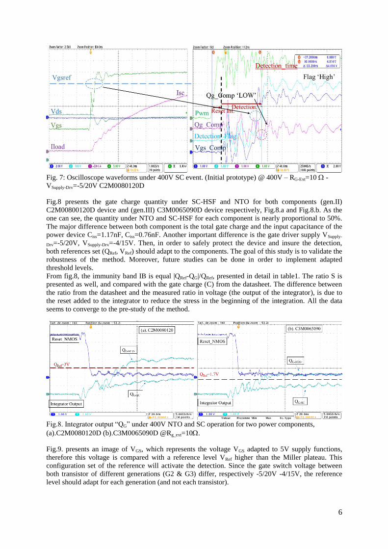
Fig. 7: Oscilloscope waveforms under 400V SC event. (Initial prototype) @ 400V – RG-Ext=10 -
VSupply-Drv=-5/20V C2M0080120D
Fig.8 presents the gate charge quantity under SC-HSF and NTO for both components (gen.II)
C2M00800120D device and (gen.III) C3M0065090D device respectively, Fig.8.a and Fig.8.b. As the
one can see, the quantity under NTO and SC-HSF for each component is nearly proportional to 50%.
The major difference between both component is the total gate charge and the input capacitance of the
power device Ciss=1.17nF, Ciss=0.76nF. Another important difference is the gate driver supply VSupply-
Drv=-5/20V, VSupply-Drv=-4/15V. Then, in order to safely protect the device and insure the detection,
both references set (QRef, VRef) should adapt to the components. The goal of this study is to validate the
robustness of the method. Moreover, future studies can be done in order to implement adapted
threshold levels.
From fig.8, the immunity band IB is equal |QRef-QG|/QRef, presented in detail in table1. The ratio S is
presented as well, and compared with the gate charge (C) from the datasheet. The difference between
the ratio from the datasheet and the measured ratio in voltage (the output of the integrator), is due to
the reset added to the integrator to reduce the stress in the beginning of the integration. All the data
seems to converge to the pre-study of the method.
Fig.8. Integrator output “QG” under 400V NTO and SC operation for two power components,
(a).C2M0080120D (b).C3M0065090D @Rg_ext=10.
Fig.9. presents an image of VGS, which represents the voltage VGS adapted to 5V supply functions,
therefore this voltage is compared with a reference level VRef higher than the Miller plateau. This
configuration set of the reference will activate the detection. Since the gate switch voltage between
both transistor of different generations (G2 & G3) differ, respectively -5/20V -4/15V, the reference
level should adapt for each generation (and not each transistor).
Page 8
7
Table I: Gate charge Immunity Band and Ratio S
Component C2M0080120D C3M0065090D
QG-NTO 4.2V 2.3V
QG-SC-HSF 1.8V 1V
QRef 3V 1.7V
IB= |QRef-QG|/QRef
NTO 0.4 0.35
SC 0.4 0.41
S%=QG-SC-HSF/QG-NTO (V/V) 43% 42%
SDS% (nC/nC) 34/71=> 48% 17.5/35 => 50%
Fig.9. “VGS image” under 400V NTO and SC operation for two power components, (a).C2M0080120
(b).C3M0065090 @RG_ext.=10.
The detection flag has been activated after 133ns including the buffer propagation time 10 ns with the
initial prototype and 118ns with the final board. The detection time does not depend only on how fast
our system is, the detection time depends obviously on the value of Rg, the input capacitance of the
power device, slew rate dvgs/dt and how low the reference level is defined (>VgsM), etc.. . The slew rate
between NTO vs SC change as presented in fig. 6-7, the Vgs comparator under NTO arrives after SC,
which is a positive thing to detect faster. Same as the reference levels, the threshold gate level was
defined at a robust level 18V, with a lower level the detection will be earlier but with a trade-off on the
SNR.
Protection of the device
After the detection of the fault, the SiC MOSFET must be turned off safely, to stop Ids from increasing
and to avoid a dangerous over-voltage. Therefore, to protect the circuit safely, a soft shut down SSD
system is included in the SMD. If the protection is not well designed it can lead to breakdown voltage
due to high negative dIds/dt caused by the total stray inductance, the protection should be soft to
prevent this phenomenon.
After activation of the D flip-flop (Detection flag), the 3-state fast driver output is turned under high
impedance (HZ), to avoid being short circuited by the SSD circuit. Then, after a delay at least
equivalent to the driver propagation time, the SSD is activated, including a serial resistance RSSD=75Ω,
to turn off softly the device through discharging the gate input capacitance. The delay has been chosen
Page 9
8
to be set at 50ns, for safety, fig.10. The observed plateau in the gate-source voltage VGS under
protection is due to the inductive effect through the kelvin inductance LSK (parasitic inductance of
package and terminal pin on PCB in the presence of a di/dt < 0).
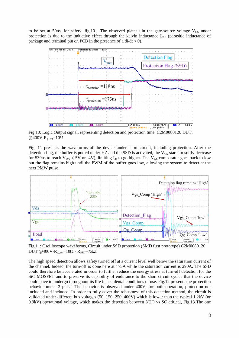
Fig.10: Logic Output signal, representing detection and protection time, C2M0080120 DUT,
@400V-Rg_ext=10.
Fig. 11 presents the waveforms of the device under short circuit, including protection. After the
detection flag, the buffer is putted under HZ and the SSD is activated, the VGS starts to softly decrease
for 530ns to reach VDrv- (-5V or -4V), limiting Ids to go higher. The VGS comparator goes back to low
but the flag remains high until the PWM of the buffer goes low, allowing the system to detect at the
next PMW pulse.
Fig.11: Oscilloscope waveforms, Circuit under SSD protection (SMD first prototype) C2M0080120
DUT @400V-Rg_ext=10 - RSSD=75Ω.
The high speed detection allows safety turned off at a current level well below the saturation current of
the channel. Indeed, the turn-off is done here at 175A while the saturation current is 290A. The SSD
could therefore be accelerated in order to further reduce the energy stress at turn-off detection for the
SiC MOSFET and to preserve its capability of endurance to the short-circuit cycles that the device
could have to undergo throughout its life in accidental conditions of use. Fig.12 presents the protection
behavior under 2 pulse. The behavior is observed under 400V, for both operation, protection not
included and included. In order to fully cover the robustness of this detection method, the circuit is
validated under different bus voltages (50, 150, 250, 400V) which is lower than the typical 1.2kV (or
0.9kV) operational voltage, which makes the detection between NTO vs SC critical, Fig.13.The one
Page 10
9
can see that with the final prototype the drain SC current is lower and stopped earlier than the previous
prototype. The current is limited around 130A.
Fig. 12: DUT before and after protection, C2M0080120 DUT @ 400V Rg_ext=10. (Initial prototype)
Fig. 13: DUT under protection for different VBus [50,150,250,400V], C2M0080120 DUT,
@Rg_ext=10.( last prototype)
Conclusion
2D diagnosis once again proves it is the perfect candidate for short circuit detection and protection. In
a first place, the gate charge method (2D diagnosis) detects as fast as possible the behavior of the
circuit, within 118ns. In the second place, the gate leakage current method, comes to confirm and
support the detection of the short-circuit, before the failure of the power transistor. With those
experiments both methods were validated. Robustness study is led for different components and VBus
values. Studies are led to finalize FUL detection in other specific mode not presented in this paper.
Moreover, the detection circuit can be further optimized and the delays can be strongly reduced. At the
end, the goal is to integrate all the functions in a dedicated gate driver Integrated Circuit in CMOS
technology, for fast detection. It is important to note that with such a fast protection, the fault current
110A < ISSD <135A
Rq : Isat 290A
Page 11
10
is limited to 135A against nearly 290A with no protection. In such a short time and at such a low
current value, the dynamic temperature of the chip remains lower than the melting temperature of the
aluminum to metal of the die, which would allow a large number of repeated short circuits without
ageing effect [14]. This last point is one of the future properties to be highlighted in the continuity of
this work.
References
[1] Baliga B.J.: Silicon Carbide Power Devices, World Scientific, 2005.
[2] Wang Z., et al.: Design and Performance Evaluation of Overcurrent Protection Schemes for Silicon Carbide
(SiC) Power MOSFETs, IEEE TIEs 61, 5570–5581 (2014).
[3] Romano G., et al.: Influence of design parameters on the short-circuit ruggedness of SiC power MOSFETs,
in 2016 28th ISPSD, juin 2016, p. 47‑ 50,
[4] Chen J., et al.: A Smart IGBT Gate Driver IC with Temperature Compensated Collector Current Sensing, in
IEEE Transactions on Power Electronics, vol. 34, no. 5, pp. 4613-4627, May 2019.
[5] Sadik D., et al.: Short-Circuit Protection Circuits for Silicon-Carbide Power Transistors, in IEEE
Transactions on Industrial Electronics, vol. 63, no. 4, pp. 1995-2004, April 2016.
[6] Awwad A. E., Dieckerhoff S.: Short-circuit evaluation and overcurrent protection for SiC power MOSFETs,
2015 17th EPE'15 ECCE-Europe, Geneva, 2015, pp. 1-9.
[7] Bertelshofer T., Maerz A., Bakran M.: Design Rules to Adapt the Desaturation Detection for SiC MOSFET
Modules, PCIM Europe 2017, Nuremberg, Germany,
[8] Bakran M., Hain S.: Integrating the New 2D — Short circuit detection method into a power module with a
power supply fed by the gate voltage, 2016 IEEE (SPEC), Auckland, 2016, pp. 1-6.
[9] Boige, F., Trémouilles D., Richardeau F.: Physical origin of the gate current surge during short-circuit
operation of SiC MOSFET, IEEE Electron Device Lett., pp. 1–1, 2019
[10] Boige F., and Richardeau F.: Gate leakage-current analysis and modelling of planar and trench power SiC
MOSFET devices in extreme short-circuit operation, Microelectron. Reliab., Sep. 2017
[11] Oberdieck K., Schuch S., DeDoncker R. W.: “Short circuit detection using the gate charge characteristic for
Trench/Fieldstop-IGBTs”, EPE'16 ECCE Europe, Karlsruhe, 2016, pp. 1-10.
[12] Horiguchi T., Kinouchi S., Nakayama Y., Akagi H.: A fast short-circuit protection method using gate
charge characteristics of SiC MOSFETs, 2015 IEEE ECCE, Montreal, QC, 2015, pp. 4759-4764.
[13] Barazi Y., Rouger N., Richardeau F.: Comparison between ig integration and vgs derivation methods
dedicated to fast short circuit 2D diagnosis for wide band gap power devices, Mathematics and
Computers in Simulation, 2020.
[14] Fayyaz A., Boige F., Borghese A., Guibaud G., Chazal V., et al.: Aging and failure mechanisms of SiC
Power MOSFETs under repetitive short- circuit pulses of different duration, ICSCRM 2019, Japan