Jason Heidecker Jet Propulsion Laboratory, California Institute of Technology
National Aeronautics and Space Administration
NEPP Electronic Technology Workshop June 11-13, 2012
1 To be presented at the 3rd NASA Electronic Parts and Packaging (NEPP) Program Electronic Technology Workshop June 11-13, 2012, NASA GSFC, Greenbelt, MD.
To be presented at the 3rd NASA Electronic Parts and Packaging (NEPP) Program Electronic Technology Workshop June 11-13, 2012, NASA GSFC, Greenbelt, MD. 2
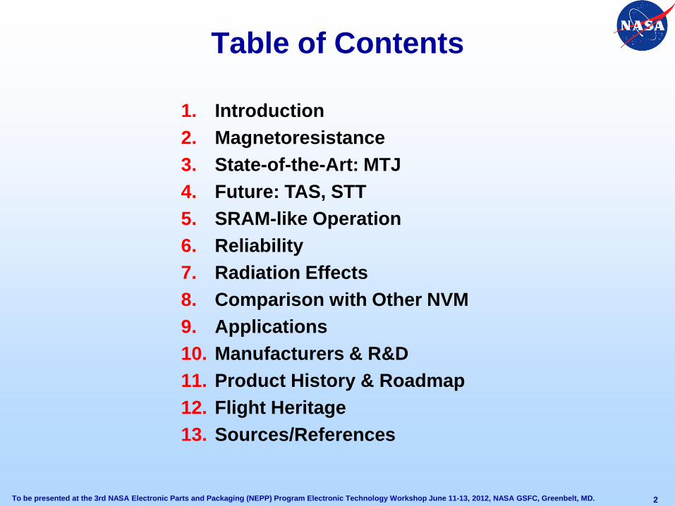
Table of Contents
1. Introduction 2. Magnetoresistance 3. State-of-the-Art: MTJ 4. Future: TAS, STT 5. SRAM-like Operation 6. Reliability 7. Radiation Effects 8. Comparison with Other NVM 9. Applications 10. Manufacturers & R&D 11. Product History & Roadmap 12. Flight Heritage 13. Sources/References
To be presented at the 3rd NASA Electronic Parts and Packaging (NEPP) Program Electronic Technology Workshop June 11-13, 2012, NASA GSFC, Greenbelt, MD.
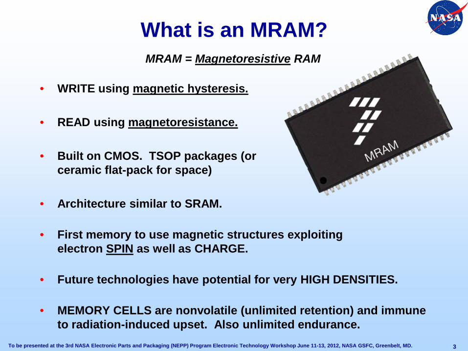
MRAM = Magnetoresistive RAM
What is an MRAM?
3
• WRITE using magnetic hysteresis.
• READ using magnetoresistance.
• Built on CMOS. TSOP packages (or ceramic flat-pack for space)
• Architecture similar to SRAM.
• First memory to use magnetic structures exploiting electron SPIN as well as CHARGE.
• Future technologies have potential for very HIGH DENSITIES.
• MEMORY CELLS are nonvolatile (unlimited retention) and immune to radiation-induced upset. Also unlimited endurance.
To be presented at the 3rd NASA Electronic Parts and Packaging (NEPP) Program Electronic Technology Workshop June 11-13, 2012, NASA GSFC, Greenbelt, MD.
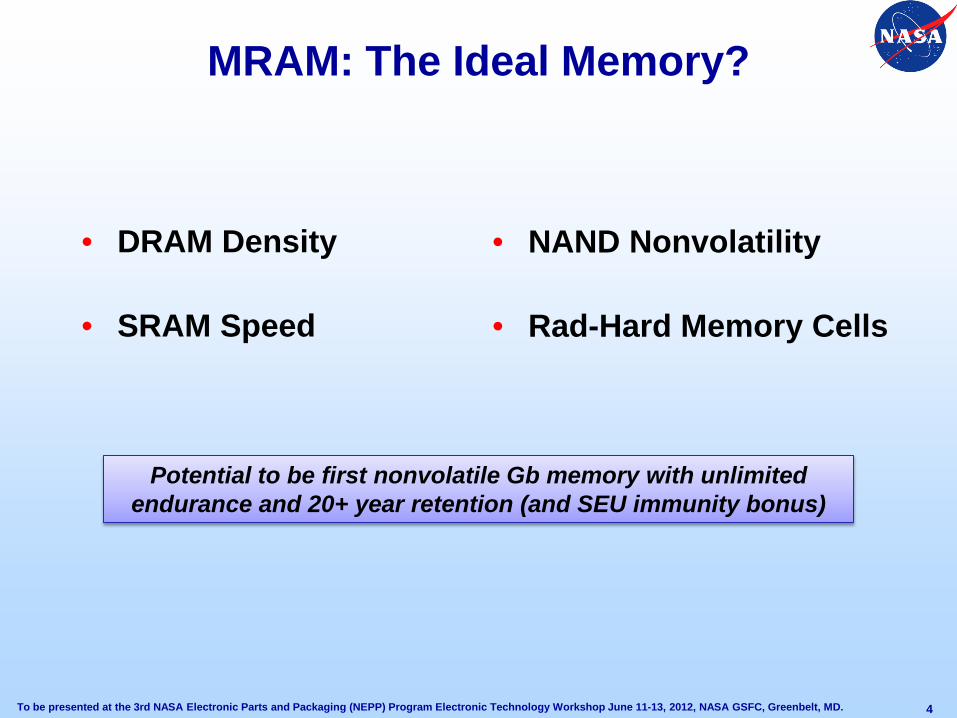
MRAM: The Ideal Memory?
4
Potential to be first nonvolatile Gb memory with unlimited endurance and 20+ year retention (and SEU immunity bonus)
• DRAM Density
• SRAM Speed
• NAND Nonvolatility
• Rad-Hard Memory Cells
To be presented at the 3rd NASA Electronic Parts and Packaging (NEPP) Program Electronic Technology Workshop June 11-13, 2012, NASA GSFC, Greenbelt, MD.
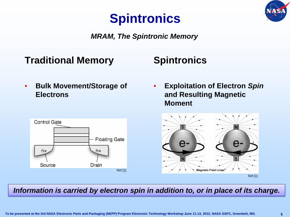
MRAM, The Spintronic Memory
Spintronics
Traditional Memory • Bulk Movement/Storage of
Electrons
5
Spintronics • Exploitation of Electron Spin
and Resulting Magnetic Moment
Information is carried by electron spin in addition to, or in place of its charge.
Ref [1]
Ref [1]
To be presented at the 3rd NASA Electronic Parts and Packaging (NEPP) Program Electronic Technology Workshop June 11-13, 2012, NASA GSFC, Greenbelt, MD.
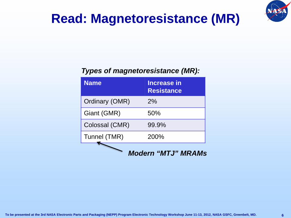
Read: Magnetoresistance (MR)
6
Types of magnetoresistance (MR): Name Increase in
Resistance Ordinary (OMR) 2%
Giant (GMR) 50%
Colossal (CMR) 99.9%
Tunnel (TMR) 200%
Modern “MTJ” MRAMs
To be presented at the 3rd NASA Electronic Parts and Packaging (NEPP) Program Electronic Technology Workshop June 11-13, 2012, NASA GSFC, Greenbelt, MD.
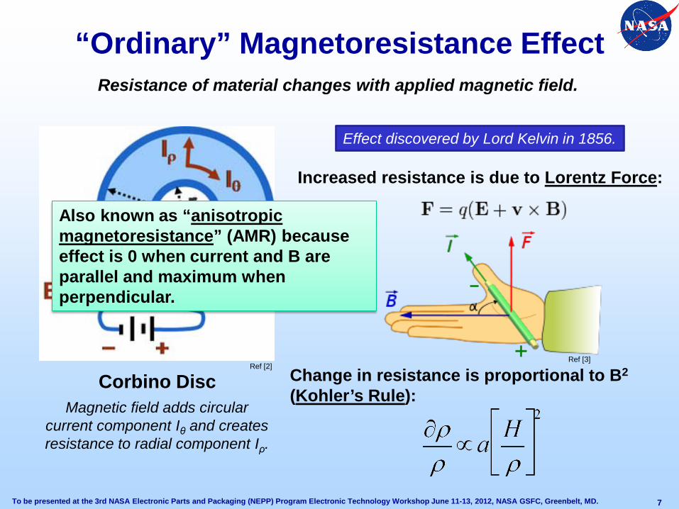
“Ordinary” Magnetoresistance Effect Resistance of material changes with applied magnetic field.
Corbino Disc Magnetic field adds circular
current component Iθ and creates resistance to radial component Iρ.
Increased resistance is due to Lorentz Force:
Change in resistance is proportional to B2 (Kohler’s Rule):
Effect discovered by Lord Kelvin in 1856.
Also known as “anisotropic magnetoresistance” (AMR) because effect is 0 when current and B are parallel and maximum when perpendicular.
7
Ref [2] Ref [3]
To be presented at the 3rd NASA Electronic Parts and Packaging (NEPP) Program Electronic Technology Workshop June 11-13, 2012, NASA GSFC, Greenbelt, MD.
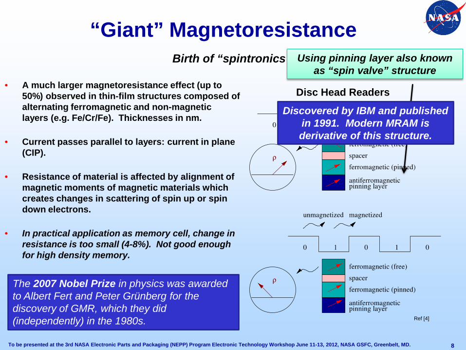
Birth of “spintronics”
“Giant” Magnetoresistance
• A much larger magnetoresistance effect (up to 50%) observed in thin-film structures composed of alternating ferromagnetic and non-magnetic layers (e.g. Fe/Cr/Fe). Thicknesses in nm.
• Current passes parallel to layers: current in plane (CIP).
• Resistance of material is affected by alignment of magnetic moments of magnetic materials which creates changes in scattering of spin up or spin down electrons.
• In practical application as memory cell, change in resistance is too small (4-8%). Not good enough for high density memory.
The 2007 Nobel Prize in physics was awarded to Albert Fert and Peter Grünberg for the discovery of GMR, which they did (independently) in the 1980s.
Disc Head Readers
8
Using pinning layer also known as “spin valve” structure
Discovered by IBM and published in 1991. Modern MRAM is derivative of this structure.
Ref [4]
To be presented at the 3rd NASA Electronic Parts and Packaging (NEPP) Program Electronic Technology Workshop June 11-13, 2012, NASA GSFC, Greenbelt, MD.
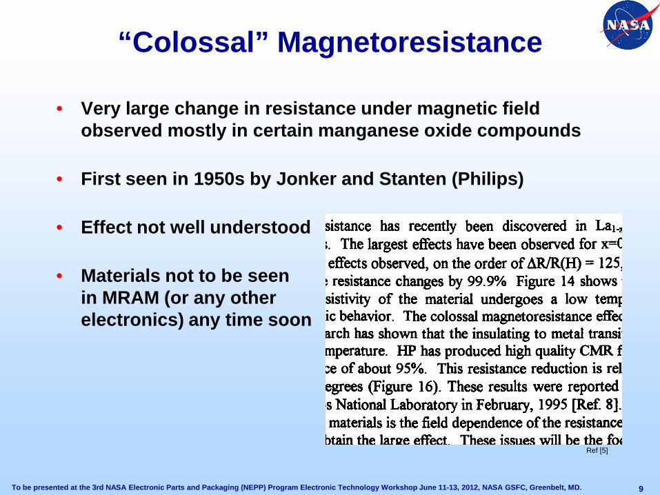
“Colossal” Magnetoresistance
• Very large change in resistance under magnetic field observed mostly in certain manganese oxide compounds
• First seen in 1950s by Jonker and Stanten (Philips)
• Effect not well understood
• Materials not to be seen in MRAM (or any other electronics) any time soon
9
Ref [5]
To be presented at the 3rd NASA Electronic Parts and Packaging (NEPP) Program Electronic Technology Workshop June 11-13, 2012, NASA GSFC, Greenbelt, MD.
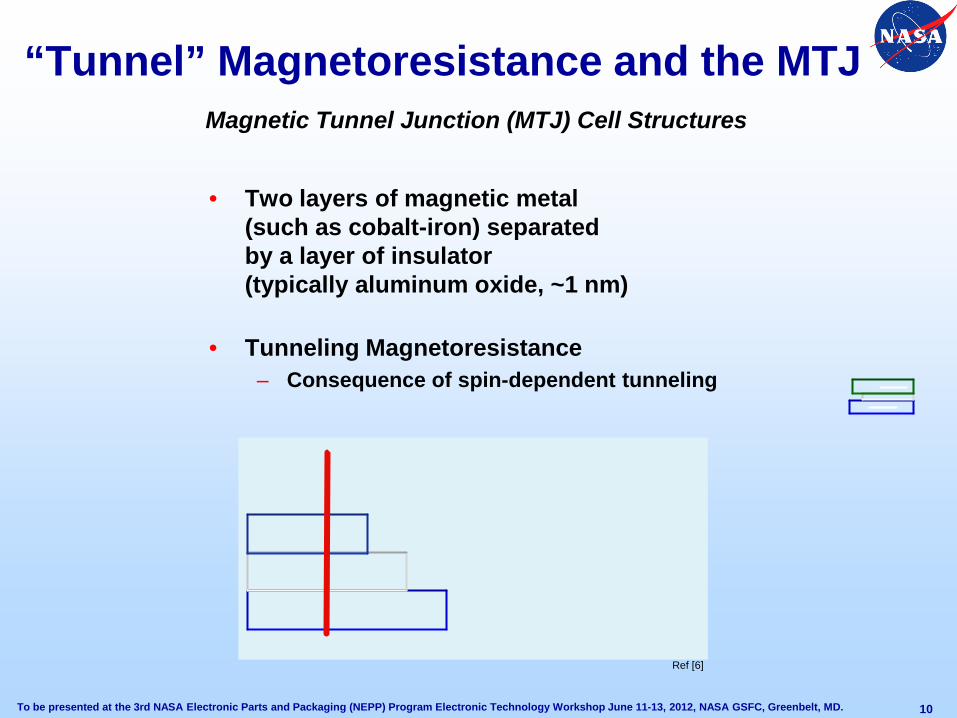
Magnetic Tunnel Junction (MTJ) Cell Structures
“Tunnel” Magnetoresistance and the MTJ
10
• Two layers of magnetic metal (such as cobalt-iron) separated by a layer of insulator (typically aluminum oxide, ~1 nm)
• Tunneling Magnetoresistance – Consequence of spin-dependent tunneling
Ref [6]
To be presented at the 3rd NASA Electronic Parts and Packaging (NEPP) Program Electronic Technology Workshop June 11-13, 2012, NASA GSFC, Greenbelt, MD.
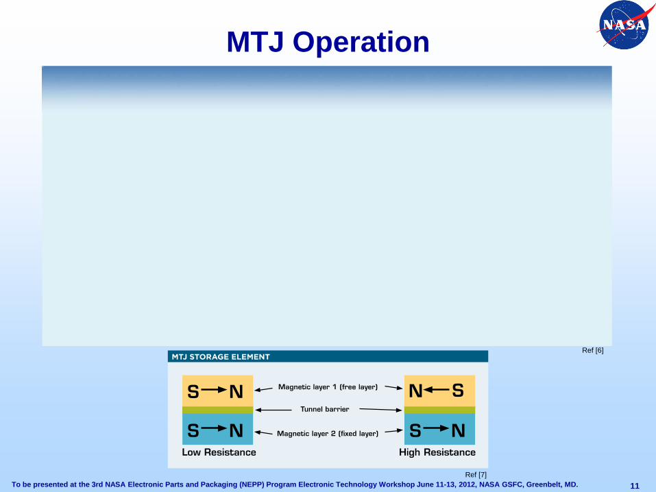
MTJ Operation
11
Ref [6]
Ref [7]
To be presented at the 3rd NASA Electronic Parts and Packaging (NEPP) Program Electronic Technology Workshop June 11-13, 2012, NASA GSFC, Greenbelt, MD.
To be presented at the 3rd NASA Electronic Parts and Packaging (NEPP) Program Electronic Technology Workshop June 11-13, 2012, NASA GSFC, Greenbelt, MD.
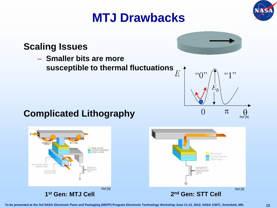
MRAM Future: Thermally Assisted Switching (TAS)
• Idea is to heat the cell, which lowers the strength of the required magnetic fields for switching
• Advantages: – Eliminates write selectivity problems: write select is
temperature driven – Lower power: only one magnetic field required for write – It is thermally stable due to the exchange bias of the
storage layer.
• Main Advocate: Crocus (Spintec spin-off): Just received $300M to build factory in Russia.
13
To be presented at the 3rd NASA Electronic Parts and Packaging (NEPP) Program Electronic Technology Workshop June 11-13, 2012, NASA GSFC, Greenbelt, MD.
To be presented at the 3rd NASA Electronic Parts and Packaging (NEPP) Program Electronic Technology Workshop June 11-13, 2012, NASA GSFC, Greenbelt, MD.
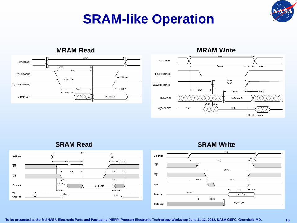
SRAM-like Operation
15
MRAM Read
SRAM Read
MRAM Write
SRAM Write
To be presented at the 3rd NASA Electronic Parts and Packaging (NEPP) Program Electronic Technology Workshop June 11-13, 2012, NASA GSFC, Greenbelt, MD.
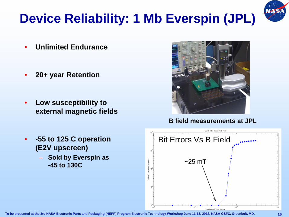
Device Reliability: 1 Mb Everspin (JPL)
• Unlimited Endurance
• 20+ year Retention
• Low susceptibility to external magnetic fields
• -55 to 125 C operation (E2V upscreen)
– Sold by Everspin as -45 to 130C
16
B field measurements at JPL
~25 mT
Bit Errors Vs B Field
To be presented at the 3rd NASA Electronic Parts and Packaging (NEPP) Program Electronic Technology Workshop June 11-13, 2012, NASA GSFC, Greenbelt, MD.
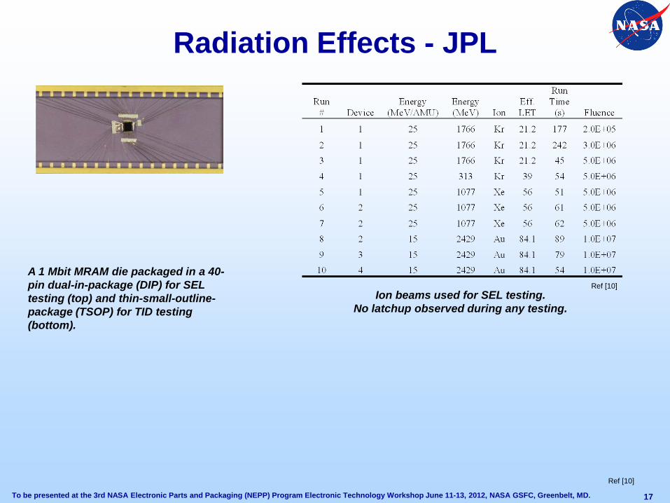
Radiation Effects - JPL
17
A 1 Mbit MRAM die packaged in a 40-pin dual-in-package (DIP) for SEL testing (top) and thin-small-outline-package (TSOP) for TID testing (bottom).
Ion beams used for SEL testing. No latchup observed during any testing.
Ref [10]
Ref [10]
To be presented at the 3rd NASA Electronic Parts and Packaging (NEPP) Program Electronic Technology Workshop June 11-13, 2012, NASA GSFC, Greenbelt, MD.
To be presented at the 3rd NASA Electronic Parts and Packaging (NEPP) Program Electronic Technology Workshop June 11-13, 2012, NASA GSFC, Greenbelt, MD.
Applications
• Home Computing – Quick boot discs, similar to Flash
• Mobile Computing
– Nonvolatility
• Military/Space – Nonvolatile, Rad-Hard
• RFID
– Embedded MRAM
19
Wherever nonvolatility, quick booting, high endurance, and/or radiation-hardness are important.
To be presented at the 3rd NASA Electronic Parts and Packaging (NEPP) Program Electronic Technology Workshop June 11-13, 2012, NASA GSFC, Greenbelt, MD.
MRAM Players (Past and Present)
20
To be presented at the 3rd NASA Electronic Parts and Packaging (NEPP) Program Electronic Technology Workshop June 11-13, 2012, NASA GSFC, Greenbelt, MD.
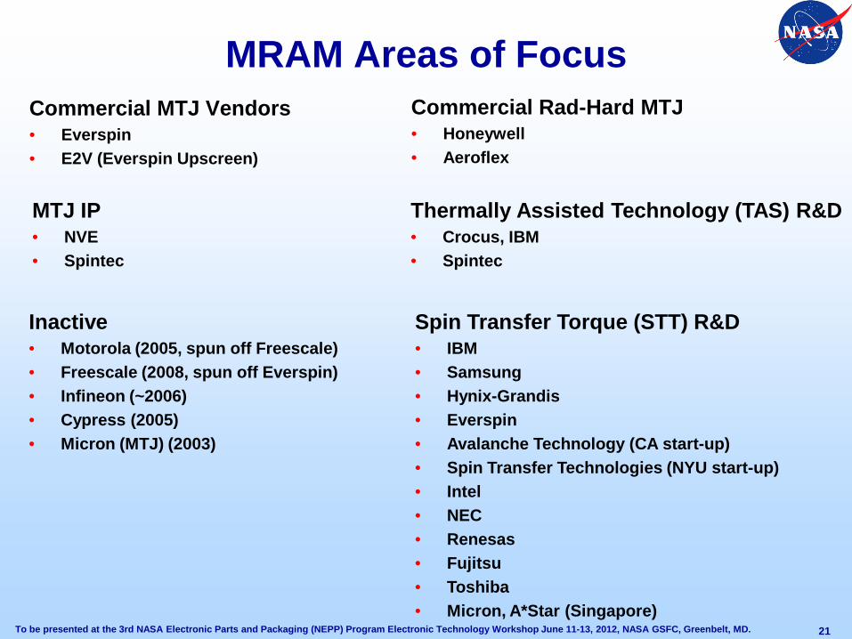
MRAM Areas of Focus Commercial MTJ Vendors • Everspin • E2V (Everspin Upscreen)
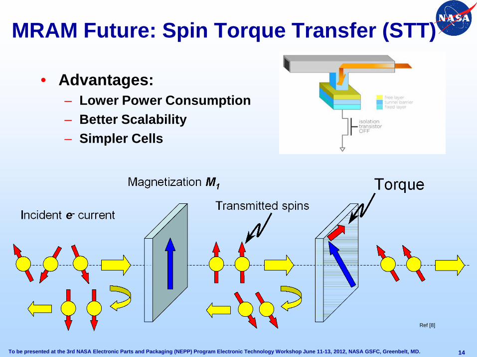
Spin Transfer Torque (STT) R&D • IBM • Samsung • Hynix-Grandis • Everspin • Avalanche Technology (CA start-up) • Spin Transfer Technologies (NYU start-up) • Intel • NEC • Renesas • Fujitsu • Toshiba • Micron, A*Star (Singapore)
Thermally Assisted Technology (TAS) R&D • Crocus, IBM • Spintec
To be presented at the 3rd NASA Electronic Parts and Packaging (NEPP) Program Electronic Technology Workshop June 11-13, 2012, NASA GSFC, Greenbelt, MD.
To be presented at the 3rd NASA Electronic Parts and Packaging (NEPP) Program Electronic Technology Workshop June 11-13, 2012, NASA GSFC, Greenbelt, MD.
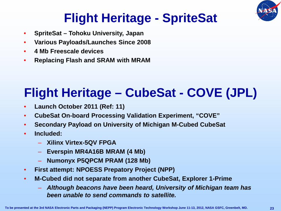
Flight Heritage – CubeSat - COVE (JPL) • Launch October 2011 (Ref: 11) • CubeSat On-board Processing Validation Experiment, “COVE” • Secondary Payload on University of Michigan M-Cubed CubeSat • Included:
• First attempt: NPOESS Prepatory Project (NPP) • M-Cubed did not separate from another CubeSat, Explorer 1-Prime
– Although beacons have been heard, University of Michigan team has been unable to send commands to satellite.
23
• SpriteSat – Tohoku University, Japan • Various Payloads/Launches Since 2008 • 4 Mb Freescale devices • Replacing Flash and SRAM with MRAM
Flight Heritage - SpriteSat
To be presented at the 3rd NASA Electronic Parts and Packaging (NEPP) Program Electronic Technology Workshop June 11-13, 2012, NASA GSFC, Greenbelt, MD.
Sources/References 1. Mustafa, J. “Design and Analysis of Future Memories Based on Switchable Resistive Elements,” 2006.